

Page 1
cPCI-6930
6U CompactPCI® Server Class Eight-Core
Intel® Xeon® E5 Processor Blade
User’s Manual
Manual Rev.: 2.02
Revision Date: November 13, 2014
Part No: 50-15080-1020
Advance Technologies; Automate the World.
Page 2

Revision History
Revision Release Date Description of Change(s)
2.00 2013/04/15 Initial release
2.01 2014/01/21 Add IPMI user’s guide
2.02 2014/11/13 Add PMC slot -12V support note
Page 3

cPCI-6930
Preface
Copyright 2013-14 ADLINK Technology Inc.
This document contains proprietary infor mation protected by copyright. All rights are reserved. No part of this manual may be reproduced by any mechanical, electronic, or other means in any form
without prior written permission of the manufacturer.
Disclaimer
The information in this document is subject to change without prior
notice in order to improve reliability, design, and function and does
not represent a commitment on the part of the manufa cturer.
In no event will the manufacturer be liable for direct, indirect, special, incidental, or consequential damages arising out of the use or
inability to use the product or documentation, even if advised of
the possibility of such damages.
Environmental Responsibility
ADLINK is committed to fulfill its social responsibility to global
environmental preservation through compliance with the European Union's Restriction of Hazardous Substances (RoHS) directive and Waste Electrical and Electronic Equipment (WEEE)
directive. Environmental protection is a top priority for ADLINK.
We have enforced measures to ensure that our products, manufacturing processes, components, and raw materials have as little
impact on the environment as possible. When products are at their
end of life, our customers are encouraged to dispose of them in
accordance with the product disposal and/or recovery programs
prescribed by their nation or company.
Trademarks
Product names mentioned herein are used for identification purposes only and may be trademarks and/or registered trademarks
of their respective companies.
Preface iii
Page 4

Using this Manual
Audience and Scope
The cPCI-6930 User’s Manual is intended for hardware
technicians and systems operators with knowledge of installing,
configuring and operating industrial grade computer systems.
Manual Organization
This manual is organized as follows:
Chapter 1, Introduction: Introduces the cPCI-6930, its features,
block diagrams, and package contents.
Chapter 2, Specifications: Presents detailed specification infor-
mation.
Chapter 3, Functional Description: Describes the cPCI-6930
main functions.
Chapter 4, Board Interfaces: Describes the cPCI-6930 board
interfaces.
Chapter 5, Getting Started: Describes the installation of compo-
nents to the cPCI-6930 and rear transition modules.
Chapter 6, Driver Installation: Provides information on how to
install the cPCI-6930 device drivers.
Chapter 7, Utilities: Describes the utilities of the cPCI-6930.
Chapter 8, BIOS Setup: Describes basic navigation for the AMI
BIOS setup utility.
Chapter 9, Checkpoints & Beep Codes: Describes the AMI
BIOS setup utility Checkpoints & Beep Codes.
Chapter 10, IPMI User Guide: Describes the Intelligent Platform
Management Interface (IPMI) specification rev. 1.5.
Important Safety Instructions: Presents safety instructions all
users must follow for the proper setup, installation and usage of
equipment and/or software.
Getting Service: Contact information for ADLINK’s worldwide
offices.
iv Preface
Page 5
cPCI-6930
Conventions
Take note of the following conventions used throughout this
manual to make sure that users perform certain tasks and
instructions properly.
Additional information, aids, and tips that help users perform
tasks.
NOTE:
NOTE:
Information to prevent minor physical injury, component damage, data loss, and/or program corruption when trying to com-
CAUTION:
WARNING:
plete a task.
Information to prevent serious physical injury, component
damage, data loss, and/or program corruption when trying to
complete a specific task.
Preface v
Page 6

This page intentionally left blank.
vi Preface
Page 7

cPCI-6930
Table of Contents
Revision History...................................................................... ii
Preface.................................................................................... iii
List of Figures........................................................................ xi
List of Tables........................................................................ xiii
1 Introduction ........................................................................ 1
1.1 Overview.............................................................................. 1
1.2 Features............................................................................... 2
1.3 Block Diagram ..................................................................... 3
1.4 Product List............................. ... .......................................... 4
1.5 Package Contents ............................................................... 5
2 Specifications..................................................................... 7
2.1 cPCI-6930 Blade Specifications .......................................... 7
2.2 I/O Connectivity ................................................................. 10
2.3 Power Requirements.................... ... .... ... ... ... ... .... ... ... ... .... . 11
3 Functional Description .................................................... 15
3.1 Processors......................................................................... 15
3.2 Chipset............................................................................... 17
3.3 PMC/XMC Site................................................................... 17
3.4 Intel® Turbo Boost Technology......................................... 18
3.5 Intel® Hyper Threading Technology.................................. 18
3.6 TPM................................................................................... 19
3.7 Battery ............................................................................... 19
4 Board Interfaces............................................................... 21
4.1 cPCI-6930 Board Layout ................................................... 21
4.2 cPCI-6930 Assembly Layout ............................................. 22
Table of Contents vii
Page 8

4.3 cPCI-6930 Front Panel ...................................................... 23
4.4 Connector Pin Assignments............................................... 24
4.5 Switches............................................................................. 37
5 Getting Started.................................................................. 39
5.1 CPU and Heatsink ............................................................. 39
5.2 2.5" SATA Drive Installation............................................... 40
5.3 CompactFlash Card Installation......................................... 47
5.4 CFast Card Installation ...... ... ............................................. 51
5.5 PMC/XMC Module Installation........................................... 54
5.6 Installing the cPCI-6930 to the Chassis............................. 59
6 Driver Installation.............................................................. 61
7 Utilities............................................................................... 63
7.1 Watchdog Timer................................................................. 63
7.2 Preboot Execution Environment (PXE).............................. 68
8 BIOS Setup........................................................................ 69
8.1 Starting the BIOS............................................................... 69
8.2 Main Setup......................................................................... 74
8.3 Advanced BIOS Setup....................................................... 75
8.4 Chipset Configuration ........................................................ 93
8.5 Boot Settings ..................................................................... 99
8.6 Security Setup.................................................................. 101
8.7 Save & Exit Menu ............................................................ 102
9 Checkpoints & Beep Codes........................................... 105
9.1 Checkpoint Ranges............................ ... .... ... ... ... ... ........... 105
9.2 Standard Checkpoints...................................................... 105
9.3 OEM-Reserved Checkpoint Ranges............................... . 114
10IPMI User Guide .............................................................. 115
10.1 Introduction........................................ ... .... ... ... ... .............. 115
10.2 Summary of Commands Supported by BMR-AVR-cPCI. 115
viii Table of Contents
Page 9

cPCI-6930
10.3 OEM Commands Summary Table................................... 117
10.4 CompactPCI Address Map .............................................. 121
10.5 Communications with IPMC............................................. 122
10.6 IPMI Sensors List............................................................. 122
10.7 Relevant Documents ....................................................... 123
Important Safety Instructions............................................ 125
Getting Service.................................................................... 127
Table of Contents ix
Page 10

This page intentionally left blank.
xTable of Contents
Page 11

cPCI-6930
List of Figures
Figure 1-1: cPCI-6930 Functional Block Diagram..............................3
Figure 4-1: cPCI-6930 Board Layout ...............................................21
Figure 4-2: cPCI-6930 Assembly Layout .........................................22
Figure 4-3: cPCI-6930 Front Panel .................................................. 23
List of Figures xi
Page 12

This page intentionally left blank.
xii List of Figures
Page 13

cPCI-6930
List of Tables
Table 2-1: cPCI-6930 Blade Specifications ...................................... 7
Table 2-2: cPCI-6930 I/O Connectivity ...........................................10
Table 4-1: cPCI-6930 Front Panel Status LED Descriptions.......... 23
List of Tables xiii
Page 14

This page intentionally left blank.
xiv List of Tables
Page 15

1 Introduction
1.1 Overview
The cPCI-6930 is a 6U CompactPCI® single board computer featuring a single 32nm Intel® Xeon® Processor E5-2400 Series with
8/6/4-cores in LGA1356 socket mated with the Intel® C604 Series
Platform Controller Hub. The cPCI-6930 supports three channels
of DDR3-1333/1600 ECC registered SDRAM in three RDIMMs
channel up to total 48GB capacity. Graphics is provided by a Silicon Motion SM750 2D GPU supporting up to 1920x1440 resolution. Four front panel 10/100/1000BASE-T ports are provided by
the Intel® 82580EB Gigabit Ethernet controller.
The cPCI-6930 Series supports a 64bit/66MHz CompactPCI bus
with optional PMC site with 32/64-bit 133MHz PCI bus or
PCI-Express x8 XMC site. The 8HP cPCI-6930 provides four GbE
ports, one VGA port, three USB 2.0 ports, two USB 3.0 ports, one
DB-9 RS-232 serial port on the front p anel. Onboard storage cap abilities include 4GB of soldered SATA NAND flash and a SATA 6
Gb/s port convertible to direct connector for an onboard 2.5" SATA
drive, CFast adapter, or CompactFlash adapter, with an onboard
2.5” SAS drive supported by BOM option (only 1
SATA /CFast/CF/SAS device supported).
A selection of optional Rear Transition Modules (RTM) provides
additional I/O functionality including two GbE ports for PICMG
2.16 support, USB 2.0 ports, PS/2 keyboard/mouse port, serial
ports, High Definition Audio, SATA ports, additional VGA/ DVI
interfaces (dependent on selected RTM), and optional CF or SD
socket. Up to eight SAS ports supporting hardware RAID via two
mini-SAS x4 connectors are available when mated with the
cPCI-R6200 RTM, and signals for two S AS ports are available on
J5 by BOM option.
cPCI-6930
For dense computing requirements, the cPCI-6930 supports operation in both a system slot and in a peripheral slot as a standalone
blade. The cPCI-6930 is compliant with the PICMG 2.9 specification and supports system management functions based on the
Intelligent Platform Management Interface (IPMI) as well as hardware monitoring of physical char acteristics such as CPU and system temperature, DC voltages and power status.
Introduction 1
Page 16

The cPCI-6930 is ideal for server-grade applications, providing
datacom equipment providers, system integrators, robust computer makers and security sectors a flexible, cost-optimized solution for mission critical applications with a reliable, smooth path for
scalability and expansion.
1.2 Features
X 6U CompactPCI® blade in 8HP width form factor
X Supports Intel® Xeon® Processor E5-2400 Series in
LGA1356 socket, up to 8-core Xeon® E5-2448L 1.8GHz,
20MB LLC
X Intel® C604 Platform Controller Hub
X Three channels of DDR3-1333/1600 ECC registered
SDRAM via three 240-pin RDIMM, up to 48GB
X 64bit/66MHz CompactPCI® Interface based on PCI specifi-
cations, universal V(I/O)
X Supports Satellite Mode operation as a standalone blade in
peripheral slots
X One 32/64-bit, 33/66/133MHz PMC or PCI-Express x8 XMC
site
X Two USB 3.0 ports via discrete controller
X 4GB SATA NAND flash soldered onboard
X SATA 6 Gb/s direct connector for onboard 2.5" drive
X Optional CFast, CompactFlash or 2.5" SAS drive support
X Eight general purpose user programmable LEDs on front
panel for (default Port 80 status)
X Dual independent RGB outputs on front panel and rear I/O
X Four Gigabit Ethernet ports on front panel
X Compliant with PICMG 2.0, 2.1, 2.9, 2.16 standards
X Infineon SLB 9635 TT1.2 TPM support upon request
2Introduction
Page 17
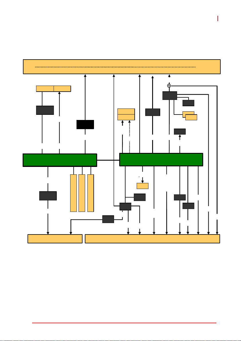
1.3 Block Diagram
cPCI-6930
Fron t Panel
PMC1 XMC 1
PCIX
64b/133M
Pericom
PI7C9X13
PCIe x8
PCIe x4
PCIe x8
Intel® Xeon® E5 Processor Family
PCIe x4
Pericom
PI7C9X13
PCI 64b/66M
DD3-1333/1600 RDIMM
IPMB 0/1
GbE 1/2/3 /4
Intel
82580
PCIe x4
DD3-1333/1600 RDIMM
COM1
DMI
DD3-1333/1600 RDIMM
IPMC
2.5” HDD
CF/CFAST
SAS/
SATA
SATA 0
LPC
SIO
COM4
KB/MS
1x USB 2.0
2x USB 2.0
SATA
SSD
TPM
COM2/3
USB 3.0
USB 3.0
PCIe x1
VGA
RGB
SM750
PCIe x1
Intel® C600 PCH
6x USB,
HDA,
5xGP IO,
RTC
SAT A 2/3/4
SAS1/2
BIOS
SPI
82574
2.16
vBIOS
vRAM
vRAM
82574
2.16
PCIe x4
DVI
RGB
J1/J2 J3/J5
Figure 1-1: cPCI-6930 Functional Block Diagram
Introduction 3
Page 18

1.4 Product List
Products included in the cPCI-6930 series are:
SBC
X cPCI-6930D: 8HP width (dual-slot) 6U CompactPCI blade
featuring single Intel® Xeon® processor with four/six/eight
cores in LGA1356 socket, three channel DDR3-1333/1600
ECC RDIMM, 4x GbE, 1x VGA, 3x USB 2.0, 2x USB 3.0, 1x
RS-232 COM, 4GB onboard NAND flash, SATA direct connector for onboard 2.5" drive (optional CFast/CF/SAS support), PMC/XMC site
Rear Transition Module
X cPCI-R6002: 6U 4HP width RTM with DVI-I, 2x COM, 3x
USB, 2x GbE, 2x SATA
X cPCI-R6002D: 6U 8HP width RTM with DVI-I, 2x COM, 5x
USB, 2x GbE, 3x SA TA, Mic-in, Line-out, PS/2 KB/MS
X cPCI-R6100: 6U 4HP width RTM with 4x GbE, 4x USB, 2x
SA TA, VGA, PS/2 KB/MS, CF & SD sockets, (Support s only
3x GbE when mating with cPCI-6930)
X cPCI-R6110: 6U 4HP width RTM with 2x GbE, 4x USB, 3x
SATA, VGA, PS/2 KB/MS, CF, & SD sockets
X cPCI-R6200: 6U 8HP width RTM with 2x GbE, 2x COM, 6x
USB, DVI-I (VGA signal only), 3x SATA, Mic-in, Line-out,
PS/2 KB/MS, 8x SAS
X cPCI-R6700D: 6U 8HP width RTM wi th on board ATI E4690
GPU, 2x DVI-I, 2x GbE, 2x COM, 6x USB, Mic-in, Line-in,
Line-out, onboard PS/2 KB/MS, 3x SATA
Adapter Kits
X DB-CFast: CFast socket kit for cPCI-6930, including
adapter board and mounting hardware
X DB-6920CF-H: CompactFlash socket kit for cPCI-6930,
including adapter board, card guide and mounting hardware
X DB-SAS: 2.5" SAS drive adapter kit for cPCI-6930 including
adapter board and mounting hardware (requires BOM
option)
4Introduction
Page 19

cPCI-6930
1.5 Package Contents
The cPCI-6930 is packaged with the following components. If any
of the items on the contents list are missing or damaged, retain the
shipping carton and packing material and contact the dealer for
inspection. Please obtain authorization before returning any product to ADLINK. The packing contents of the cPCI-6930 are
non-standard configurations and may vary depending on customer
requests.
Processor Blade
X cPCI-6930
Z CPU and memory specifications will differ depending on
options selected
Z Thermal module is assembled on the board
X 2.5" SATA drive accessory pack
X ADLINK All-in-One DVD
X User’s manual
Optional Accessories
X DB-CFast: CFast socket kit for cPCI-6930, including
adapter board and mounting hardware
X DB-6920CF-H: CompactFlash socket kit for cPCI-6930,
including adapter board, card guide and mounting hardware
X DB-SAS: 2.5" SAS drive adapter kit for cPCI-6930 including
adapter board and mounting hardware (requires BOM
option)
The contents of non-standard cPCI-6930 configurations may
vary depending on the customer’s requirements.
NOTE:
NOTE:
This product must be protected from static discharge and physical shock. Never remove any of the components except at a
CAUTION:
Introduction 5
static-free workstation. Use the anti-static bag shipped with the
product when putting the board on a surface. Wear an
anti-static wrist strap properly grounded on one of the system's
ESD ground jacks when installing or servicing system components.
Page 20

This page intentionally left blank.
6Introduction
Page 21

2 Specifications
2.1 cPCI-6930 Blade Specifications
cPCI-6930
CompactPCI®
Standards
Mechanical • Standard 6U CompactPCI®
Processor 32nm Intel® Xeon® processor in LGA1356 socket
Chipset • Intel® BD82C604 Platform Controller Hub (PCH)
Host Memory • Three channel DDR3-1333/1600 ECC registered memory
CompactPCI
Bus
PMC/XMC • One 32/64-bit, 33/66/133MHz PMC site or PCI-Express x8
Graphics • Silicon Motion SM750 2D GPU
Gigabit
Ethernet
• PICMG® 2.0 CompactPCI® Rev. 3.0
• PICMG® 2.1 Hot Swap Specification Rev.2.0
• PICMG® 2.9 System Management Bus Rev. 1.0
• PCIMG® 2.16 Packet Switching Backplane Rev.1.0
• Board size: 233.35mm x 160mm
• Dual slot (8HP, 40.64mm) width for cPCI-6930D
• CompactPCI® connectors with J1, J2, J3 and J5
• 8-core Xeon® Processor E5-2448L, 1.8 GHz, 20MB LLC
cache, TDP 70W
• 6-core Xeon® Processor E5-2428L, 1.8 GHz, 15MB LLC
cache, TDP 60W
• 4-core Xeon® Processor E5-2418L, 2.0 GHz, 10MB LLC
cache, TDP 50W
• Passive heatsink
• Three RDIMM sockets
• Up to 48GB (dependent on availability of memory modules)
• PCI 64-bit/66MHz; 3.3V, 5V universal V(I/O)
• Supports operation in system slot as master or in peripheral
slot as standalone blade without connectivity to
CompactPCI bus (Satellite mode)
XMC site on DB-6930L2 riser card
• 16MB embedded 32-bit DDR memory at 166MHz
• One analog RGB output to front panel VGA port; second
RGB output to J3.
• Supports resolutions up to 1920x1440
• One Intel® 82580 Gigabit Ethernet controller for 4x
10/100/1000BASE-T ports on front panel
• Two Intel® 82574L Gigabit Ethernet controllers for 2x
10/100/1000BASE-T port to J3 for PICMG 2.16
Table 2-1: cPCI-6930 Blade S pecifications
Specifications 7
Page 22
Serial Ports Up to three 16C 550 serial ports
• One DB-9 RS-232 serial port on front panel
• Two serial ports routed to rear I/O through J3
USB • Two USB 3.0 ports on front panel
• Three USB 2.0 ports on front panel, six ports routed to J3
KB/MS • PS/2 Keyboard/Mouse port to J3
Audio • High Definition Audio signals routed to J3
TPM Infineon SLB 9635 TPM
• Over/Under voltage detection
• Low/High frequency sensor/filter
• Reset filter
• Memory Encryption/Decryption
Storage
Interface
1
• Onboard 4GB SA TA NAND flash
• One SATA 6 Gb/s direct connector for 2.5" onboard
HDD/SDD (removable)
1
• Optional CompactFlash socket onboard via DB-CF - SA
adapter board (shares space with SATA direct connector)
• Optional CFast socket onboard via DB-CFAST adapter
board (shares space with SATA direct connector)
• Optional SAS direct connector for 2.5" onboard drive
(shares space with SATA direct connector; not available
concurrently with COM, USB, PMC/XMC site on layer 2 requires BOM option)
BIOS • AMI EFI BIOS, 64Mbit SPI flash memory
Faceplate I/O • 4x 10/100/1000BASE-T Ethernet ports
• 1x VGA port
• 3x USB 2.0 ports
• 2x USB 3.0 ports
• 1x DB-9 COM port
• PMC/XMC slot
OS
Compatibility
• Microsoft Windows 7 32/64-bit
• Microsoft Windows Server 2008 32/64-bit
• Red Hat Enterprise Linux 6.1 x86 64-bit
• Fedora 15 x86 64-bit
• Other OS support on request
Table 2-1: cPCI-6930 Blade Specifications
8 Specifications
Page 23

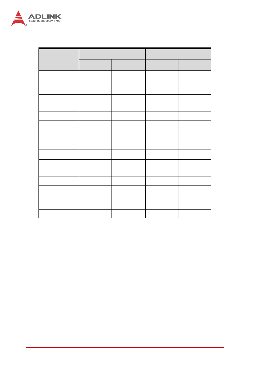
Environmental • Operating Temperature2:
Standard: 0 to 55°C with forced air flow
ETT: -20°C to 70°C with forced air flow
• Storage Temperature: -40°C to 85°C
• Humidity: 95% non-condensing
• Shock: 15G pe ak-to-peak, 11ms duration, non-operating
•Vibration
3
: Operating 2 Grms, 5-500Hz, each axis w/o hard
drive
EMI • CE EN55022
• FCC Class A
Table 2-1: cPCI-6930 Blade S pecifications
Notes:
1. The SATA direct connector is removable (DB-6920SAT) and
can be replaced with a CompactFlash socket adapter (DB-CFSC) or CFast socket adapter. A CompactFlash card, CFast
card and SATA drive cannot be used simultaneously.
2. ADLINK-certified thermal de sign. The thermal performance is
dependent on the chassis cooling design. Sufficient forced airflow is required (see 2.4 "Thermal Requirements"). Temperature limit of optional mass storage devices may affect the thermal specification.
3. The storage device limits the operational vibration. When application requires higher specification for anti-vibration, it is recommended to use a flash storage device.
cPCI-6930
Specifications 9
Page 24
2.2 I/O Connectivity
cPCI-6930 RTM
1
Faceplate Onboard J3 J5
Gigabit
Ethernet
Y x4 — Y x2 —
COM Y x1 — Y x2 —
USB 2.0 Y x3 — Y x6 —
USB 3.0 Y x2 — —
VGA Y x1 — Y x1 —
Serial ATA — Y x1 Y x3 —
SAS
CF
CFast
—
—
—
2
Y
4
Y
5
Y
—
——
——
Y x2
3
PS/2 KB/MS — — Y x1 —
HDA —— Y—
LEDs Y x4 — — —
GP LEDs Y x8 — — —
Clear CMOS
Button
—Y——
Reset Button Y———
Table 2-2: cPCI-6930 I/O Connectivity
Notes:
1. Signals are passed through to the RTM. Available functions are
dependent on the specific RTM selected.
2. Available by BOM option and with DB-SAS adapter board;
shares space with SATA connector; not available concurrently
with COM, USB, PMC/XMC site on layer 2.
3. Available by BOM option (not compatible with cPCI-R6002D RTM).
4. Optional with DB-CF-SC adapter.
5. Optional with DB-CFAST adapter.
10 Specifications
Page 25

cPCI-6930
2.3 Power Requirements
In order to guarantee a stable functionality of the system, it is recommended to provide more power than the system requires. An
industrial power supply unit should be able to provide at least
twice as much power as the entire system requires of each
voltage. An ATX power su pply unit should be able to provide at
least three times as much power as the entire system requires of
each voltage.
The tolerance of the voltage lines described in the CompactPCI
specification (PICMG 2.0 R3.0) is +5%/-3% for 5, 3. 3 V and ±5%
for ±12V. This s pecification is for power delivered to each slot and
it includes both the power supply and the backplane tolerance.
Voltage
5V +5.0 VDC +5% / -3% 50 mV
3.3V +3.3 VDC +5% / -3% 50 mV
+12V +12 VDC +5% / -5% 240 mV
-12V -12 VDC +5% / -5% 240 mV
V I/O (PCI I/O
Buffer Voltage)
GND
Nominal
Value
+3.3 VDC or
+5 VDC
Tolerance
+5% / -3% 50 mV
Max. Ripple
(P - P)
Specifications 11
Page 26
Power Consumption
This section provides information on the power consumption of the
cPCI-6930 when using Intel® Xeon® E5 family processors with 3x
4GB DDR3-1333 RDIMM memory and onboard 320 GB SATA hard
disk. The cPCI-6930 is powered by 5V and 3.3V. Power consumption at 100% CPU usage was measured by running Intel Power
Thermal Utility , Version 1.4.
Turbo Boost, EIST and Hyper-Threading Technology disabled.
8-core Intel® Xeon® Processor E5-2448L, 1.8GHz, TDP 70W
OS/Mode Current 5V (A) Current 3.3V (A) Total Power (W)
DOS/Idle mode 6.44 3.87 44.97
Windows XP/Idle mode 3.53 4.50 32.50
Windows XP/
100% CPU usage
6-core Intel® Xeon® Processor E5-2428L, 1.8GHz, TDP 60W
OS/Mode Current 5V (A) Current 3.3V (A) Total Power (W)
DOS/Idle mode 6.53 3.81 45.22
Windows XP/Idle mode 16.15 4.62 31.40
Windows XP/
100% CPU usage
83.65 14.69 98.34
66.6 14.95 81.55
4-core Intel® Xeon® Processor E5-2418L, 2.0 GHz, TDP 50W
OS/Mode Current 5V (A) Current 3.3V (A) Total Power (W)
DOS/Idle mode 5.41 3.76 39.46
Windows XP/Idle mode 3.23 4.34 30.47
Windows XP/
100% CPU usage
12 Specifications
10.46 4.4 66.95
Page 27

cPCI-6930
Turbo Boost, EIST and Hyper-Threading Technology enabled.
8-core Intel® Xeon® Processor E5-2448L, 1.8GHz, TDP 70W
OS/Mode Current 5V (A) Current 3.3V (A) Total Power (W)
DOS/Idle mode 6.49 3.88 45.25
Windows XP/Idle mode 3.40 4.48 21.78
Windows XP/
100% CPU usage
19.58 4.64 113.21
6-core Intel® Xeon® Processor E5-2428L, 1.8GHz, TDP 60W
OS/Mode Current 5V (A) Current 3.3V (A) Total Power (W)
DOS/Idle mode 6.51 3.81 45.12
Windows XP/Idle mode 3.28 4.34 30.72
Windows XP/
100% CPU usage
15.51 4.51 92.43
4-core Intel® Xeon® Processor E5-2418L, 2.0 GHz, TDP 50W
OS/Mode Current 5V (A) Current 3.3V (A) Total Power (W)
DOS/Idle mode 5.42 3.75 39.48
Windows XP/Idle mode 3.29 4.36 30.84
Windows XP/
100% CPU usage
11.72 4.38 73.05
Specifications 13
Page 28

This page intentionally left blank.
14 Specifications
Page 29

3 Functional Description
The following sections describe the cPCI-6930 features and
functions.
3.1 Processors
The Intel® Xeon® processor E5 family is the next generation of
64-bit, multi-core enterprise processor built on 32-nanometer process technology. Based on a new micro-architecture, the processor is designed for a two-chip platform. The two-chip platform
consists of a processor and Platform Controller Hub (PCH). The
platform enables higher performance, lower cost, easier validation, and improved x-y footprint. The processor is designed for
servers. Included in this family of processors is an integrated
memory controller (IMC) and integrated I/O (IIO) (such as PCI
Express and DMI2) on a single silicon die
cPCI-6930
Features
Clock 1.8 GHz 1.8 GHz 2.0 GHz
Max. Single Core Turbo
Freq.
Last Level Cache 20 MB 15 MB 10 MB
No. of Cores/Threads 8/16 6/12 4/8
Maximum Power (TDP
T
junction,MAX
Memory Type DDR3-1600 DDR3-1333 DDR3-1333
2
Intel® Xeon®
1
)
E5-2448L
2.1GHz 2GHz 2.1GHz
70 W 60 W 50 W
100°C 100°C 100°C
Intel® Xeon®
E5-2428L
Intel® Xeon®
E5-2418L
Notes:
1. The highest expected sustainable power while running known
power intensive applications. TDP is not the maximum power
that the processor can dissipate.
2. The maximum supported opera ting temperature.
Functional Description 15
Page 30

Supported Technologies
X Intel® Virtualization Technology (Intel® VT)
X Intel® Virtualization Technology (Intel® VT-x)
X Intel® Trusted Execution Technology (Intel® TXT)
X Intel® Hyper-Threading Technology
X Intel® 64 Architecture
X Intel® Turbo Boost Technology
X AES New Instructions
Interfaces
X Three channels of DDR3 memory with one RDIM M pe r
channel
X Memory DDR3 data transfer rates of 80 MT/s, 1666 MT/s,
1333 MT/s, and 1600 MT/s
X 64-bit wide channels plus 8-bits of ECC support for each
channel
X DDR3 standard I/O V o ltage of 1.5 V and DDR3 Low Voltage
of 1.35V
X 1-Gb, 2-Gb, and 4-Gb DDR3 DRAM technologies supported
for RDIMM x4 and x8 devices
Z The largest memory capacity possible is 48 GB, assum-
ing three-channel mode with three x8, dual-ranked,
un-buffered, ECC, RDIMM memory configuration.
X The PCI Express ports are fully-compliant with the PCI
Express Base Specification, Revision 2.0.
16 Functional Description
Page 31

cPCI-6930
3.2 Chipset
The cPCI-6930 incorporates the Intel® C604 Platform Controller
Hub (PCH).
Intel® C604 Platform Controller Hub
X PCI Express Base Specification, Revision 2.0 support for up
to eight ports with transfer rate up to 5 GT/s
X ACPI Power Management Logic Support, Revision 4.0a
X Enhanced DMA controller, interrupt controller, and timer
functions
X Integrated Serial ATA host controllers with independent
DMA operation on up to six ports
X USB host interface with two EHCI high-speed USB 2.0 Host
controllers and two rate matching hubs provide support for
up to fourteen USB 2.0 ports
X Integrated 10/100/1000 Gigabit Ethernet MAC with System
Defense
X System Management Bus (SMBus) Specification, Version
2.0 with additional support for I2C devices
X Supports Intel® High Definition Audio
X Supports Intel® Rapid Storage Technology
X Supports Intel® Virtualization Technology for Directed I/O
X Integrated Clock Controller
X Analog and Digital Display ports
X Low Pin Count (LPC) interface
X Firmware Hub (FWH) interface support
X Serial Peripheral Interface (SPI) support
3.3 PMC/XMC Site
The cPCI-6930 supports one PMC or XMC site for front panel I/O
expansion. The PMC site provides a maximum 32/64-bit,
33/66/133MHz PCI bus link using a Pericom PI7C9X130
PCIe-to-PCI-X bridge and PCIe x4 link. The PMC site supports
+3.3V and 5V signaling. The XMC site provides a PCIe x8 lane.
Functional Description 17
Page 32

3.4 Intel® Turbo Boost Technology
Intel Turbo Boost Technology is a feature that allows the processor
to opportunistically and automatically run faster than its rated
operating core and/or render clock frequency when there is sufficient power headroom, and the product is within specified temperature and current limits. The Intel Turbo Boost Technology feature
is designed to increase performance of both multi-threaded and
single-threaded workloads. The processor supports a Turbo mode
where the processor can use the thermal capacity associated with
package and run at power levels higher than TDP power for short
durations. This improves the system responsiveness for short,
bursty usage conditions.
Turbo Mode availability is independent of the number of active
cores; however, the Turbo Mode frequency is dynamic and dependent on the instantaneous application power load, the number of
active cores, user configurable settings, operating environment,
and system design. If the power, current, or thermal limit is
reached, the processor will automatically reduce the frequency to
stay with its TDP limit.
3.5 Intel® Hyper Threading Technology
The processor supports Intel® Hyper-Threading Technology
(Intel® HT Technology), that allows an execution core to function
as two logical processors. While some execution resources (such
as caches, execution units, and buses) are shared, each logical
processor has its own architectural state with its own set of general-purpose registers and control registers. This feature must be
enabled using the BIOS and requires operating system support.
18 Functional Description
Page 33

cPCI-6930
3.6 TPM
The cPCI-6930 is equipped with the Infineon SLB 9635 TT 1.2
Trusted Platform Module (TPM), a security controller with cryptographic functionality that provides users a secure environment in
e-commerce transactions and Internet communications. The key
features provided by the TPM are:
X Hardware hash accelerator for SHA-1 algorithm
X Advanced Crypto Engine (ACE) for asymmetric key oper ations
(up to 2048-bit key length) to make hardware protection.
X Tick counter to extend the time required to decipher the key
X Over/Under-voltage detection to monitor the system stabil-
ity. If the voltage fluctuates dramatically, this function can
block the data transfer and lock the chip.
X Low/High frequency sensor to detect the IC clock fre-
quency. If the frequency fluctuates dramatically, this function can block the data transfer and lock the chip.
X Reset filter to filter reset signal in order to break the time se t
by tick counter is received
X Memory encryption to protect memory
X Physical shield in the IC to protect the die from intruding or
hacking by matching the data transferred on the 2 layer
metal shield on the IC. If the data is not matched, the IC
may be blocked.
3.7 Battery
The cPCI-6930 is provided with a 3.0V “coin cell” lithiu m battery
for the Real Time Clock (RTC). The lithium battery must be
replaced with an identical battery or a battery type recommended
by the manufacturer.
Functional Description 19
Page 34

This page intentionally left blank.
20 Functional Description
Page 35

4 Board Interfaces
This chapter illustrates the board layout, connector pin
assignments, and jumper settings of the cPCI-6930.
4.1 cPCI-6930 Board Layout
SW2
cPCI-6930
CN6
DIMM1/2/3
U24
PCH
CPU
BT1
J5
CN8
J3
J2
J1
CN11
CN12
CN13
CN14
CN16
CN9
CN7
CNX2
CNX3
CNX1
SW5
CPU CPU socket CN1/2/3/4 GbE ports
PCH Intel C604 PCH CN8 DB-6920SAT conn.
U24 Intel GbE 82580EB CN16 VGA connector
BT1 Battery CN9/7 USB 2.0 ports
DIMM1~3 RDIMM sockets CNX1 USB 3.0 ports
SW2 Clear CMOS button CNX2/CNX3 Info LEDs
SW5 Reset button CN6 DB-6930L2
J1/J2/J3/J5 cPCI connectors
board-to-board conn.
Figure 4-1: cPCI-6930 Board Layout
Board Interfaces 21
Page 36

4.2 cPCI-6930 Assembly Layout
The dual-slot width cPCI-6930 is comprised of the cPCI-6930 single-slot main board and the DB-6930L2 riser card to provide a
PMX/XMC site.
DB-6930L2
Figure 4-2: cPCI-6930 Assembly Layout
22 Board Interfaces
Page 37

4.3 cPCI-6930 Front Panel
Figure 4-3: cPCI-6930 Front Panel
Status LEDs
LED Color Condition Indication
Power
HotSwap
WDT
HDD
USB 2.0
Green
Blue
Red
Amber
St atus LEDs PMC/XMC COM
Rese t Button GbE 1/2/3/4
VGA
USB
2.0
USB 3.0
Info
LED
OFF System is off
ON System is on
Blink
Fail to power on
(payload power failure)
OFF Handles closed, System is on
Fast Blink
ON
Preparing to shut down system
(LED: 0.1s on, 0.9s off.)
Handles open and blade ready
to be removed
Voltages out of tolerance:
1
Slow Blink
3.3V, 5V, 12V, 1.5V over ±5%
(LED 2s on, 1s off)
OFF No Watchdog event
ON Watchdog event alert
OFF No drive activity
Blink
SATA, CF data read/write in
process
cPCI-6930
Table 4-1: cPCI-6930 Front Panel Status LED Descriptions
Note1:
Disabled by default. See “OemSetBlueLEDLongBlinking” on
page 118
Board Interfaces 23
Page 38

4.4 Connector Pin Assignments
See “cPCI-6930 Board Layout” on page 21 for connector locations.
USB 2.0 Connectors
Pin # Signal Name
1Vcc
2UV03UV0+
4GND
USB 3.0 Connectors
Pin # Signal Name
1 USB3.0_P5VA
2 USB2_CMAN
3 USB2_CMAP
4GND
5 USB3A_CMRXN
6 USB3A_CMRXP
7GND
8 USB3A_CMTXN
9 USB3A_CMTXP
4
3
2
1
VGA Connector (DB-15)
Signal Name Pin # Pin # Signal Name
Red 1 2 Green
Blue 3 4 N.C.
GND 5 6 GND
GND 7 8 GND
+5V. 9 10 GND
N.C. 11 12 CRTDATA
HSYNC 13 14 VSYNC
CRTCLK 15
24 Board Interfaces
Page 39

Gigabit Ethernet Connectors (RJ-45)
Pin # GbE Signal
1 LAN_TX0+
2LAN_TX03 LAN_TX1+
4 LAN_TX2+
5LAN_TX26LAN_TX17 LAN_TX3+
8 LAN_TX3+
cPCI-6930
81
Speed Activity
Status (CN4, CN5)
Network link is not established
or system powered off
10 Mbps
100 Mbps
1000 Mbps
Link OFF ON
Active OFF Blinking
Link Green ON
Active Green Blinking
Link Amber ON
Active Amber Blinking
Serial Port (DB-9)
Pin # RS-232
1 DCD-L
2RXD
3TXD
4DTR-L
5GND
6DSR-L
7RTS-L
8CTS-L
9NC
Speed LED
(Green/Amber)
OFF OFF
6
Activity LED
(Amber)
1
5
Board Interfaces 25
Page 40

Serial ATA Connector on DB-6930SAT
Pin # Signal
S1 GND
S2 TX+
S3 TXS4 GND
S5 RXS6 RX+
S7 GND
P1 NC
P2 NC
P3 NC
P4 GND
P5 GND
P6 GND
P7 5V
P8 5V
P9 5V
P10 GND
P11 Reserved
P12 GND
P13~P15 12V
S1
Signal
S7
P1
Power
P15
26 Board Interfaces
Page 41

DB-6930L2 Board-to-Board Connector (CN6)
cPCI-6930
Signal Name Pin # Pin # Signal Name
GND 1 2 GND
PCIE-A-TXN0 3 4 PCIE-A-RXN0
PCIE-A-TXP0 5 6 PCIE-A-RXP0
GND 7 8 GND
PCIE-A-TXN1 9 10 PCIE-A-RXN1
PCIE-A-TXP1 11 12 PCIE-A-RXP1
GND 13 14 GND
PCIE-A-TXN2 15 16 PCIE-A-RXN2
PCIE-A-TXP2 17 18 PCIE-A-RXP2
GND 19 20 GND
PCIE-A-TXN3 21 22 PCIE-A-RXN3
PCIE-A-TXP3 23 24 PCIE-A-RXP3
GND 25 26 GND
PCIE-A-CLKN 27 28 PCIE-B-CLKN
PCIE-A-CLKP 29 30 PCIE-B-CLKP
GND 31 32 GND
PCIE-B-TXN0 33 34 PCIE-B-RXN0
PCIE-B-TXP0 35 36 PCIE-B-RXP0
GND 37 38 GND
PCIE-B-TXN1 39 40 PCIE-B-RXN1
PCIE-B-TXP1 41 42 PCIE-B-RXP1
GND 43 44 GND
PCIE-B-TXN2 45 46 PCIE-B-RXN2
PCIE-B-TXP2 47 48 PCIE-B-RXP2
GND 49 50 GND
PCIE-B-TXN3 51 52 PCIE-B-RXN3
PCIE-B-TXP3 53 54 PCIE-B-RXP3
GND 55 56 GND
PCIE-B-TXN4 57 58 PCIE-B-RXN4
PCIE-B-TXP4 59 60 PCIE-B-RXP4
GND 61 62 GND
199 120
1 2
Board Interfaces 27
Page 42

Signal Name Pin # Pin # Signal Name
PCIE-B-TXN5 63 64 PCIE-B-RXN5
PCIE-B-TXP5 65 66 PCIE-B-RXP5
GND 67 68 GND
PCIE-B-TXN6 69 70 PCIE-B-RXN6
PCIE-B-TXP6 71 72 PCIE-B-RXP6
GND 73 74 GND
PCIE-B-TXN7 75 76 PCIE-B-RXN7
PCIE-B-TXP7 77 78 PCIE-B-RXP7
GND 79 80 GND
USB_N 81 82 XMC-RST
USB_P 83 84 USB_OC1
GND 85 86 RESET
COM-RTS 87 88 GND
COM-DTR 89 90 COM-RX
COM-CTS 91 92 COM-TX
COM-RI 93 94 COM-DSR
IPMI_DBR_TX 95 96 COM-DCD
IPMI_DBR_RX 97 98 SMBUS-DAT
GND 99 100 SMBUS-CLK
+5V 101 102 GND
+5V 103 104 +3.3V
+5V 105 106 +3.3V
+5V 107 108 +3.3V
+5V 109 110 +3.3V
+5V 111 112 +3.3V
+5V 113 114 +3.3V
+5V 115 116 +3.3V
+12V 117 118 +5V_STB
+12V 119 120 -12V
DB-6930L2 Board-to-Board Connector Pin Definition (cont’d)
28 Board Interfaces
Page 43

DB-6930SA T Connecto r (CN8)
cPCI-6930
Signal Name Pin # Pin # Signal Name
GND 1 2 GND
GND 3 4 GND
GND 5 6 GND
GND 7 8 GND
GND 9 10 GND
GND 11 12 GND
GND 13 14 GND
GND 15 16 GND
GND 17 18 GND
GND 19 20 GND
GND 21 22 GND
GND 23 24 GND
GND 25 26 GND
GND 27 28 GND
GND 29 30 GND
P3V3 31 32 P5V
P3V3 33 34 P5V
P3V3 35 36 P5V
P3V3 37 38 P5V
P1V8 39 40 NC
P1V8 41 42 NC
P1V8 43 44 NC
GND 45 46 GND
GND 47 48 SATA-TXN0
GND 49 50 SATA-TXP0
SATA-RXN0 51 52 GND
SATA-RXP0 53 54 GND
GND 55 56 RESET#
GND 57 58 GND
GND 59 60 GND
59 60
1 2
Board Interfaces 29
Page 44

PMC Connector on DB-6930-L2 (JN1, JN2)
Pin# JN1 Signal JN2 Signal
1 PMC_TCK P12V
2 N12V* PMC_TRST-L
3 GND PMC_TMS
4 PCIX_INTA-L NC (PMC_TDO)
5 PCIX_INTB-L PMC_TDI
6PCIX_INTC-L GND
7PMC_MOD-L1 GND
8P5V NC
9PCIX_INTD-L NC
10 NC NC
11 GND PMC_MOD-L2
12 P3V3_PMCAUX P3V3
13 CLK66_PCIX_PMC PMC_RST-L
14 GND PMC_MOD-L3
15 GND P3V3
16 PCIX_GNT-L0 PMC_MOD-L4
17 PCIX_REQ-L0 PMC_PME-L
18 P5V GND
19 PMC_VIO PCIX_AD30
20 PCIX_AD31 PCIX_AD29
21 PCIX_AD28 GND
22 PCIX_AD27 PCIX_AD26
23 PCIX_AD25 PCIX_AD24
24 GND PCIX_AD23
25 GND PMC_IDSEL
26 PCIX_CBE-L3 PCIX_AD23
27 PCIX_AD22 P3V3
28 PCIX_AD21 PCIX_AD20
29 PCIX_AD19 PCIX_AD18
30 P5V GND
31 PCIX_FRAME-L PCIX_AD16
32 PCIX_AD17 PCIX_CBE-L2
64
63
1 2
*Note: -12V signal not supported on JN1 pin 2. Contact ADLINK for
more information.
30 Board Interfaces
Page 45

Pin# JN1 Signal JN2 Signal
33 PCIX_FRAME-L GND
34 GND NC
35 GND PCIX_TRDY-L
36 PCIX_IRDY-L P3V3
37 PCIX_DEVSEL-L GND
38 P5V PCIX_STOP-L
39 PCIX_PCIXCAP PCIX_PERR-L
40 PCIX_LOCK-L GND
41 NC P3V3
42 NC PCIX_SERR-L
43 PCIX_PAR PCIX_CBE-L1
44 GND GND
45 PMC_VIO PCIX_AD14
46 PCIX_AD15 PCIX_AD13
47 PCIX_AD12 PCIX_M66EN
48 PCIX_AD11 PCIX_AD10
49 PCIX_AD9 PCIX_AD8
50 P5V P3V3
51 GND PCIX_AD7
52 PCIX_CBE-L0 NC
53 PCIX_AD6 P3V3
54 PCIX_AD5 NC
55 PCIX_AD4 NC
56 GND GND
57 PMC_VIO NC
58 PCIX_AD3 NC
59 PCIX_AD2 GND
60 PCIX_AD1 NC
61 PCIX_AD0 PCIX_ACK64-L
62 P5V P3V3
63 GND GND
64 PCIX_REQ64-L NC
PMC Connector Pin Definition (cont’d)
cPCI-6930
Board Interfaces 31
Page 46

XMC Connector on DB-6930L2
F1 F19
A1
A19
Pin# A B C D E F
1
2
3
4
5
6
7
8
9
10
11
12
13
14
15
16
17
18
19
RXP RXN 3.3V NC NC VPWR
GND GND Not used GND GND PCIE_RST-L
NC NC 3.3V NC NC VPWR
GND GND Not used GND GND Not used
NC NC 3.3V NC NC VPWR
GND GND Not used GND GND +12V
NC NC 3.3V NC NC VPWR
GND GND Not used GND GND -12V
NC NC Not used NC NC VPWR
GND GND Not used GND GND GA0
TXP TXN Not used NC NC VPWR
GND GND GA1 GND GND Not used
NC NC 3.3V NC NC VPWR
GND GND GA2 GND GND Not used
NC NC Not used NC NC VPWR
GND GND Not used GND GND Not used
NC NC Not used NC NC NC
GND GND Not used GND GND Not used
CK-P CK-N Not used Not used Not used Not used
32 Board Interfaces
Page 47

cPCI-6930
CompactPCI J1 Connector Pin Assignment
Pin Z A B C D E F
25 GND +5V REQ64# ENUM# +3.3V +5V GND
24 GND AD1 +5V V(I/O) AD0 ACK64# GND
23 GND P3V3 CPCI_AD4 CPCI_AD3 P5V CPCI_AD2 GND
22 GND CPCI_AD7 GND P3V3 CPCI_AD6 CPCI_AD5 GND
21 GND P3V3 CPCI_AD9 CPCI_AD8 CPCI_M66EN CPCI_CBE-L0 GND
20 GND CPCI_AD12 GND VIO CPCI_AD11 CPCI_AD10 GND
19 GND P3V3 CPCI_AD15 CPCI_AD14 GND CPCI_AD13 GND
18 GND CPCI_SERR-L GND P3V3 CPCI_PAR CPCI_CBE-L1 GND
17 GND P3V3 IPMB_CLK IPMB_DAT GND CPCI_PERR-L GND
16 GND CPCI_DEVSEL-L GND VIO CPCI_STOP-L CPCI_LOCK-L GND
15 GND P3V3 CPCI_FRAME-L CPCI_IRDY-L NC CPCI_TRDY-L GND
12-14 GND Key Area Key
11 GND CPCI_AD18 CPCI_AD17 CPCI_AD16 GND CPCI_CBE-L2 GND
10 GND CPCI_AD21 GND P3V3 CPCI_AD20 CPCI_AD19 GND
9 GND CPCI_CBE-L3 NC CPCI_AD23 GND I CPCI_AD22 GND
8 GND CPCI_AD26 GND VIO CPCI_AD25 CPCI_AD24 GND
7 GND CPCI_AD30 CPCI_AD29 CPCI_AD28 GND CPCI_AD27 GND
6 GND CPCI_REQ-L0 GND P3V3 CPCI_CLK0 CPCI_AD31 GND
5 GND NC NC CPCI_RESET-L GND CPCI_GNT-L0 GND
4 GND P5V_IPMB CPCI_HEALTHY-L VIO NC NC GND
3 GND CPCI_IRQA-L CPCI_IRQB-L CPCI_IRQC-L P5V CPCI_IRQD-L GND
2 GND cPCI_TCK-L P5V cPCI_TMS-L NC cPCI_TDI-L GND
1 GND P5V N12V cPCI_TRST-L P12V P5V GND
Board Interfaces 33
Page 48

CompactPCI J2 Connector Pin Assignment
Pin Z A B C D E F
22 GND GA4 GA3 GA2 GA1 GA0 GND
21 GND CLK6 GND NC NC NC GND
20 GND CLK5 GND NC GND NC GND
19 GND GND GND NC NC NC GND
18 GND NC NC NC GND NC GND
17 GND NC GND RSTBTN# REQ6#
16 GND NC NC DEG# GND NC GND
15 GND NC GND FAL# REQ5# GNT5# GND
14 GND AD35 AD34 AD33 GND AD32 GND
13 GND AD38 GND V(I/O) AD37 AD36 GND
12 GND AD42 AD41 AD40 GND AD39 GND
11 GND AD45 GND V(I/O) AD44 AD43 GND
10 GND AD49 AD48 AD47 GND AD46 GND
9 GND AD52 GND V(I/O) AD51 AD50 GND
8 GND AD56 AD55 AD54 GND AD53 GND
7 GND AD59 GND V(I/O) AD58 AD57 GND
6 GND AD63 AD62 AD61 GND AD60 GND
5 GND CBE5# GND V(I/O) CBE4# PAR64 GND
4 GND V(I/O) NC CBE7# GND CBE6# GND
3 GND CLK4 GND GNT3# REQ4# GNT4# GND
2 GND CLK2 CLK3 SYSEN# GNT2# REQ3# GND
1 GND CLK1 GND REQ1# GNT1# REQ2# GND
GNT6#
GND
34 Board Interfaces
Page 49

cPCI-6930
CompactPCI J3 Pin Assignment
Pin Z A B C D E F
19 GND HDA_RST# HDA_SYNC HDA_BIT_CLK HDA_SDOUT HDA_SDIN0 GND
18 GND HDA_SDIN1 HDA_SDIN2 NC HDA_DOCK_EN# HAD_DOCK_RST# GND
17 GND KBDATA KBCLK NC MSDATA MSCLK GND
16 GND SATA-TX4+ SATA -TX4- GND SATA -TX3+ SATA -TX3- GND
15 GND GND GND NC GND GND GND
14 GND SATA -RX4+ SATA -RX4- GND SATA -RX3+ SATA -RX3- GND
13 GND COM3-TX COM3-RX COM2-DCD# I2C_CLK I2C_DAT GND
12 GND COM2-RX COM2-TX COM2-DTR# COM2-DSR# COM2-RTS# GND
11 GND COM2-CTS# COM2-RI# RGB-BLUE RGB-RED RGB-GREEN GND
10 GND USB-OC4# RGB-DDCCLK RGB-DDCDAT RGB-HSYNC RGB-VSYNC GND
9GND USB-P4+ USB-P4- GND USB-P5+ USB-P5- GND
8GND USB-P6+ USB-P6- GND USB-P7+ USB-P7- GND
7GND USB-P8+ USB-P8- GND USB-P9+ USB-P9- GND
6GND USB-OC5# USB-OC6# USB-OC7# USB-OC8# USB-OC9# GND
5GNDLAN4_TXD1+ LAN4_TXD1- GND LAN4_TXD3+ LAN4_TXD3- GND
4GNDLAN4_TXD0+ LAN4_TXD0- GND LAN4_TXD2+ LAN4_TXD2- GND
3GNDLAN3_TXD1+ LAN3_TXD1- GND LAN3_TXD3+ LAN3_TXD3- GND
2GNDLAN3_TXD1+ LAN3_TXD0- GND LAN3_TXD2+ LAN3_TXD2- GND
1 GND P5V P5V P12V P5V P5V GND
High Definition Audio
Keyboard/Mouse
Serial A TA
Serial ports
USB ports
Ethernet ports
RGB
Board Interfaces 35
Page 50

CompactPCI J5 Pin Assignment
Pin Z A B C D E F
22 GND PCIE-TX0+ PCIE-TX0- GND PCIE-RX0+ PCIE-RX0- GND
21 GND PCIE-TX1+ PCIE-TX1- GND PCIE-RX1+ PCIE-RX1- GND
20 GND PCIE-TX2+ PCIE-TX2- GND PCIE-RX2+ PCIE-RX2- GND
19 GND PCIE-TX3+ PCIE-TX3- GND PCIE-RX3+ PCIE-RX3- GND
18 GND GND GND GND GND GND GND
17 GND PCIE-CLK+ PCIE-CLK- GND RESET# NC GND
16 GND GND GND RTC GND GND GND
15 GND NC NC GND NC NC GND
14 GND GPIO1 GPIO2 GPIO3 GPIO4 GPIO5 GND
13 GND NC NC GND NC NC GND
12 GND NC NC GND NC NC GND
11GNDNC NCNCNC NCGND
10 GND LAN4_100# LAN3_100# NC LAN3_1G# LAN4_1G# GND
9 GND NC NC GND SATA-TX3+ SATA-TX3- GND
8 GND NC NC GND SATA-RX3+ SATA-RX3- GND
7 GND NC NC NC NC NC GND
6GNDSAS_TXP1* SAS_TXN1* GND SAS_TXP2* SAS_TXN2* GND
5GNDSAS_RXP1* SAS_RXN1* GND SAS_RXP2* SAS_RXN2* GND
4 GND NC NC GND NC NC GND
3 GND NC NC GND NC NC GND
2 GND NC NC GND NC NC GND
1 GND NC LAN5_LINK_ACT# +3.3V LAN6_LINK_ACT# +3.3V GND
PCI Express
GPIO
SAS*
SATA
LAN
*Pins A5, B5, D5, C5, A6, B6, D6, C6 are not connected (NC)
by default. The SAS signals are only available by BOM option
NOTE:
NOTE:
as they are incompatible with the cPCI-R6002D RTM.
36 Board Interfaces
Page 51

cPCI-6930
4.5 Switches
See “cPCI-6930 Board Layout” on page 21 for switch locations.
System Reset Button (SW5)
The cPCI-6930 comes with a system reset button on the front
panel. Press switch SW5 to reset the system.
Clear CMOS Button (SW2)
The cPCI-6930 comes with a clear CMOS button to reset the
CMOS values to default. Press the switch SW2 to load the
BIOS default setting.
Board Interfaces 37
Page 52

This page intentionally left blank.
38 Board Interfaces
Page 53

5 Getting Started
This chapter describes the installation of the following component s
to the cPCI-6930 and rear transition modules:
X 2.5"SATA/SAS Drive
X CompactFlash card
X CFast Card Installation
X PMC/XMC Module Installation
5.1 CPU and Heatsink
The cPCI-6930 comes with CPU(s) and heatsink pre-installed.
Removal of heatsink/CPU by users is not recommended. Please
contact your ADLINK service representative for assistance.
cPCI-6930
Getting Started 39
Page 54

5.2 2.5" SATA Drive Installation
The cPCI-6930 series provide space to install a slim type 2.5”
SATA drive.
1. 1.Find the 2.5" SATA drive daughter board DB-6920SAT
and screw kit in the package.
2. Remove the 5 screws securing the DB-6930L2 shown
below.
40 Getting Started
Page 55

cPCI-6930
3. Remove the 4 screws from the front panel as shown
below.
4. Remove the DB-6930L2 daughter board.
Getting Started 41
Page 56

5. Find the standoffs in the screw pack and attach them to
the 2.5" drive as shown below. Plug the SATA drive
adapter board DB-6920SAT into the SATA drive.
6. Align and assemble the connector on the DB-6920SAT
to the cPCI-6930's onboard SATA connector (CN8).
42 Getting Started
Page 57

cPCI-6930
7. Secure the SATA drive assembly with two screws shown
as below.
8. There are four screws and four lock washers in the
screw pack.
Getting Started 43
Page 58

9. Place the lock washers on the screws.
10.Turn over the board (solder side up) and fasten the
screws as shown below.
44 Getting Started
Page 59

cPCI-6930
11.Reinstall the DB-6930L2 daughter board by securing the
screws removed in step 2 above.
12.Replace the screws on the front panel removed in step 3
above.
Getting Started 45
Page 60

13.The SATA drive assembly installation is completed.
2.5” SAS Drive Installation
If you have ordered the SAS BOM option, follow the above instructions using the 2.5" SAS drive daughter board included in the
DB-SAS adapter kit. and follow the above procedure to install the
SAS drive.
The SAS drive installation procedure is the same as that for a
SATA drive.
NOTE:
NOTE:
46 Getting Started
Page 61

cPCI-6930
5.3 CompactFlash Card Installation
The cPCI-6930 Series provides space to install a CompactFlash
card. The CompactFlash adapter can be purchased using the
ordering code DB-6920CF-H.
1. Find the CompactFlash adapter DB-6920CF-H in the
CompactFlash kit.
2. Refer to “2.5” SATA Drive Installation, steps 2 to 4 to
remove the DB-6930L2 daughter board
3. Find the screws and standoffs in the CompactFlash kit
4. Install the standoffs and screws to the CompactFlash
adapter board as shown.
Getting Started 47
Page 62

5. Place tw o standoffs on the adapter board in the m ounting locations indicated by the arrows, and align the two
mounting holes on the adapter board with the soldered
standoffs circled below.
48 Getting Started
Page 63

cPCI-6930
6. Find the two flathead screws shown below in the Com-
pactFlash kit.
7. With the DB-6920CF-H adapter board aligned as shown,
press it onto the onboard SATA connector (CN8). Use
the two flathead screws to fasten the CompactFlash
adapter board.
Getting Started 49
Page 64

8. Turn the cPCI-6930 board over (solder side up) and
secure the CompactFlash adapter board with the 2
remaining screws.
9. The CompactFlash adapter board assembly installation
is completed.
50 Getting Started
Page 65

cPCI-6930
5.4 CFast Card Installation
The cPCI-6930 Series provides space to install a CompactFlash
card. The CompactFlash adapter can be purchased using the
ordering code DB-CFast.
1. A CFast card can be installed on the onboard SATA con-
nector (CN8). The CFast card shares the same space as
the 2.5" SATA drive.
2. Refer to “2.5” SATA Drive Installation, steps 2 to 4 to
remove the DB-6930L2 daughter board
3. Find the standoffs in the CFast kit
4. Place the standoffs on top of the onboard standoffs as
shown below.
Getting Started 51
Page 66

5. Find the CFast adapter board in CFast adapter kit.
6. Remove the card retaining bracket by removing the two
screws shown below on the back of the adapter board.
Insert the CFast card into the adapter board and secure
the CFast card by replacing the retaining bracket with
the two screws.
52 Getting Started
Page 67

cPCI-6930
7. Align the CFast adapter board with the onboard SATA
connector (CN8) and locate the two screws in the CFast
adapter kit.
8. Secure the CFast adapter board by fastening the screws
as shown below.
9. Refer to SATA hard drive installation steps 11 ~ 12 to
replace the DB-6930L2 daughter board and complete
the assembly.
Getting Started 53
Page 68

5.5 PMC/XMC Module Installation
The 8HP cPCI-6930D Series provides space to install a PMC or
XMC module.
1. To install a PMC/XMC module, first begin removing the
DB-6930L2 daughter board by removing the five screws
shown below.
2. Remove the four screws as shown below on the front
panel and remove the DB-6930L2 daughter board from
the blade assembly.
54 Getting Started
Page 69

cPCI-6930
3. Position the hard drive assembly on the cPCI-6930 so
that the standoffs on the hard drive align with the screw
holes on the board, and the connector on the
DB-6930SAT adapter board is aligned with the
board-to-board connector (CN6).
Getting Started 55
Page 70

4. Secure four screws provided by PMC/XMC supplier to
the solder side of the DB-6930L2.
5. Remove the filler plate on the front panel.
56 Getting Started
Page 71

cPCI-6930
6. Install the PMC/XMC module and DB-6930L2 daughter
board assembly onto the cPCI-6930D and secure the
five screws shown below.
7. Secure the four screws on the front panel.
Getting Started 57
Page 72

8. Mezzanine card installation is completed.
58 Getting Started
Page 73

cPCI-6930
5.6 Installing the cPCI-6930 to the Chassis
The cPCI-6930 may be installed in a system or peripheral slot of a
6U CompactPCI chassis. These instructions are for reference
only. Refer to the user guide that comes with the chassis for more
information.
1. Be sure to select the correct slot depending on the oper-
ational purpose of the module. The system power may
now be powered on or off.
2. Remove the blank face cover from the selected slot, if
necessary.
3. Press down on the release catches of the cPCI-6930
ejector handles.
4. Remove the black plastic caps securing the mounting
screws to the front panel.
5. Align the module’s top and bottom edges to the chassis
card guides, and then carefully slide the module into the
chassis. A slight resistance may be felt when inserting
the module. If the resistance it too strong, check if there
are bent pins on the backplane or if the board’s connector pins are not properly aligned with connectors on the
backplane. Then push the board until it is completely
flush with the chassis.
6. Push the ejector handles outwards to secure the module
in place, and then fasten the screws on the module front
panel.
7. Connect the cables and peripherals to the board, and
then turn the chassis on if necessary.
Getting Started 59
Page 74

This page intentionally left blank.
60 Getting Started
Page 75

6 Driver Installation
The cPCI-6930 drivers are available from the ADLINK All-In-One
CD at X:\cPCI\cPCI-6930\, or from the ADLINK website
(http://www.adlinktech.com). ADLINK provides validated drivers for Windows 7 32-bit. We recommend using these drivers to
ensure compatibility. The VxWorks BSP can be downloaded from
the cPCI-6930 product page on the ADLINK website.
The following describes the driver installation procedures for Windows 7:
1. Install the Windows operating system before installing
any driver. Most standard I/O device drivers are installed
during Windows installation.
2. Install the chipset driver by extracting and running the
executable program in ...\Chipset\Intel Chipset Device
Software_ Win7_2008_All_9.2.3.1013.zip.
3. Install the LAN drivers for the 82580 controller by
extracting and running the executable program in
…\LAN\Intel 82580 Gigabit Network Connection_
WIN7_32_11.14.43.0.zip.
4. Install the graphics driver and utilities by extracting and
running the executable program in ...\Graphics\Silicon
Motion SM750_Win7_2008_32_6.13.1.31.zip.
5. Install the Audio driver by extracting and running the
executable program in …\Audio\RealTek_High Defini-
tion Audio_WIN7_2008_32_6.0.1.6.0.1.6410.zip.
cPCI-6930
6. Install the USB 3.0 driver by extracting and running the
executable program in …\USB3.0\Texas Instruments
XHCI Controller Win7_2008_All_1.12.7.0.zip.
7. Install the AHCI/RAID utilities by extracting and running
the executable program in …\AHCI\Intel Rapid Storage
Technology_3.0.0.1112.zip
8. Install the TPM utilities by extracting and running the
executable program in …\TPM\Infineon Trusted Plat-
form Module_Win7_2008_32_2.1.1.0.zip
Driver Installation 61
Page 76

62 Driver Installation
Page 77

7 Utilities
7.1 Watchdog Timer
This section describes the operation of the cPCI-6930’s watchdog
timer (WDT). The primary function of the WDT is to monitor the
cPCI-6930's operation and to reset the system if a software application fails to function as prog rammed. The following WDT functions may be controlled using a software application:
X enabling and disabling
X reloading timeout value
The cPCI-6930 custom WDT circuit is implemented using the
internal IO of the Winbond SuperIO W83627UHG which is at 2 Eh
of LPC. The basic functions of the WDT include:
X Starting the timer countdown
X Enabling or disabling WDT
X Enabling or disabling WDT countdown LED ON
X Reloading the timeout value to keep the watchdog from tim-
ing out
X Setting the range of the timeout period from 1 to 15300 seconds
X Sending a RESET signal to the system when the watchdog
times out
cPCI-6930
Using the Watchdog in an Application
The following section describes using the WDT functions in an
application. The WDT reset function is explained in the previous
section. This can be controlled through the registers in the cPCI6930's SuperIO.
An application using the reset fe ature enab les the watch dog func tion, sets the count-down period, and reloads the timeout value
periodically to keep it from resetting the system. If the timer countdown value is not reloaded, the watchdog resets the system hardware after its counter reaches zero.
ADLINK provides a demo DOS utility in the ADLINK All-In-One
CD. You can find it in the following directory: X:\cPCI\cPCI6930\WDT.
Utilities 63
Page 78

Sample Code
The sample program written in C shown below offers an interactive way to test the Watchdog Timer under DOS.
#include<stdio.h>
#include<dos.h>
static unsigned int W83627UHG_ioPort = 0x2e;
void Enter_W83627UHG_Config(unsigned int flag)
{
if(flag) W83627UHG_ioPort = 0x4e;
outportb(W83627UHG_ioPort, 0x87);
outportb(W83627UHG_ioPort, 0x87);
}
void Get_W83627UHG_ID(unsigned int &ID1, unsigned int
&ID2)
{
outportb(W83627UHG_ioPort, 0x20);
ID1 = inportb(W83627UHG_ioPort+1);
outportb(W83627UHG_ioPort, 0x21);
ID2 = inportb(W83627UHG_ioPort+1);
}
void W83627UHG_WDT_Run(unsigned int count_value, unsigned
int PLEDflag)
{
unsigned int tempCount, registerValue;
outportb(W83627UHG_ioPort, 0x07);
outportb(W83627UHG_ioPort+1, 8); // CR07 set Logical
Device 8
if(count_value >= 60)
{
outportb(W83627UHG_ioPort, 0xf5);
registerValue = inportb(W83627UHG_ioPort+1);
registerValue |= 0x04;
outportb(W83627UHG_ioPort+1, registerValue); /
/ set Minute mode
64 Utilities
Page 79

tempCount = count_value / 60;
if((count_value%60) > 30)
tempCount++;
if(tempCount > 255)
tempCount = 255;
printf("WDT timeout in %d minutes.\n",
tempCount);
}
else
{
outportb(W83627UHG_ioPort, 0xf5);
registerValue = inportb(W83627UHG_ioPort+1);
registerValue &= 0xfb;
outportb(W83627UHG_ioPort+1, registerValue); /
/ set second mode
tempCount = count_value;
}
if(tempCount)
{
outportb(W83627UHG_ioPort, 0x30);
registerValue = inportb(W83627UHG_ioPort+1);
registerValue |= 0x01;
outportb(W83627UHG_ioPort+1, registerValue); /
/ set WDTO# and PLED are active.
cPCI-6930
outportb(W83627UHG_ioPort, 0xf5);
registerValue = inportb(W83627UHG_ioPort+1);
registerValue |= 0x02;
outportb(W83627UHG_ioPort+1, registerValue); /
/ Enable KCB reset.
if(PLEDflag)
{
outportb(W83627UHG_ioPort, 0x07);
outportb(W83627UHG_ioPort+1, 9); // CR07
set Logical Device 9
outportb(W83627UHG_ioPort, 0x30);
registerValue =
inportb(W83627UHG_ioPort+1);
Utilities 65
Page 80

registerValue |= 0x02; // set GPIO2 is
active
outportb(W83627UHG_ioPort+1,
registerValue);
outportb(W83627UHG_ioPort, 0xe4);
registerValue =
inportb(W83627UHG_ioPort+1);
registerValue &= 0xf7; // set GPIO23 is
output function
outportb(W83627UHG_ioPort+1,
registerValue);
outportb(W83627UHG_ioPort, 0xe5);
registerValue =
inportb(W83627UHG_ioPort+1);
registerValue &= 0xf7; // set GPIO23 is
Low
outportb(W83627UHG_ioPort+1,
registerValue);
}
printf("WDT timeout in %d seconds.\n",
tempCount);
}
else
{
outportb(W83627UHG_ioPort, 0x07);
outportb(W83627UHG_ioPort+1, 9); // CR07 set
Logical Device 9
outportb(W83627UHG_ioPort, 0x30);
registerValue = inportb(W83627UHG_ioPort+1);
registerValue |= 0x02; // set GPIO2 is active
outportb(W83627UHG_ioPort+1, registerValue);
outportb(W83627UHG_ioPort, 0xe4);
registerValue = inportb(W83627UHG_ioPort+1);
registerValue &= 0xf7; // set GPIO23 is output
function
outportb(W83627UHG_ioPort+1, registerValue);
outportb(W83627UHG_ioPort, 0xe5);
66 Utilities
Page 81

registerValue = inportb(W83627UHG_ioPort+1);
registerValue |= 0x08; // set GPIO23 is High
outportb(W83627UHG_ioPort+1, registerValue);
printf("WDT is Disabled.\n");
}
outportb(W83627UHG_ioPort, 0x07);
outportb(W83627UHG_ioPort+1, 8); // CR07 set Logical
Device 8
outportb(W83627UHG_ioPort, 0xf6);
outportb(W83627UHG_ioPort+1, tempCount); // set WDT
count value..
}
void Exit_W83627UHG_Config(unsigned int flag)
{
if(flag) W83627UHG_ioPort = 0x4e;
outportb(W83627UHG_ioPort, 0xaa);
cPCI-6930
Utilities 67
Page 82

7.2 Preboot Execution Environment (PXE)
The cPCI-6930 supports the Intel® Preboot Execution Environment (PXE) that is capable of booting up or executing an OS
installation through an Ethernet ports. To use PXE, there must be
a DHCP server on the network with one or more servers running
PXE and MTFTP services. It could be a Windows® 2003 server
running DHCP, PXE, and MTFTP services or a dedicated DHCP
server with one or more additional servers running PXE and
MTFTP services.
To build a network environment with PXE support:
1. Setup a DHCP server with PXE tag configuration
2. Install the PXE and MTFTP services
3. Make a boot image file on the PXE server (i.e. the boot server)
4. Enable the PXE boot function on the client computer
68 Utilities
Page 83

8 BIOS Setup
The following chapter describes basic navigation for the AMI EFI
BIOS setup utility.
8.1 Starting the BIOS
To enter the setup screen, follow these steps:
1. Power on the motherboard
2. Press the < Delete > key on your keyboard when you
see the following text prompt:
< Press DEL to run Setup >
3. After you press the < Delete > key, the main BIOS setup
menu displays. You can access the other setup screens
from the main BIOS setup menu , such as Chipset and
Power menus.
cPCI-6930
Note: In most cases, the < Delete > key is used to invoke the setup
screen. There are several cases that use other keys, such as
< F1 >, < F2 >, and so on.
BIOS Setup 69
Page 84

Setup Menu
The main BIOS setup menu is the first screen that you can navigate. Each main BIOS setup menu option is described in this
user’s guide.
The Main BIOS setup menu screen has two main frames. The left
frame displays all the options that can be configured. “Grayed”
options cannot be configured, “Blue” options can be.
The right frame displays the key legend. Above the key legend is
an area reserved for a text message. When an option is selected
in the left frame, it is highlighted in white. Often a text message will
accompany it.
Navigation
The BIOS setup/utility uses a key-based navigation system called
hot keys. Most of the BIOS setup utility hot keys can be used at
any time during the setup navigation process.
70 BIOS Setup
Page 85

NOTE:
NOTE:
cPCI-6930
There is a hot key legend located in the right frame on most
setup screens.
The < F8 > key on your keyboard is the Fail-Safe key. It is not displayed on the key legend by default. To set the Fail-Safe settings
of the BIOS, press the < F8 > key on your keyboard. It is located
on the upper row of a standard 101 keyboard. The Fail-Safe settings allow the motherboard to boot up with the least amount of
options set. This can lessen the probability of conflicting settings.
Hotkey Descriptions
Enter The < Enter > key allows you to display or change the setup
option listed for a particular setup item. The < Enter > key
can also allow you to display the setup sub-screens.
F1 The < F1 > key allows you to display the General Help
screen. Press the < F1 > key to open the General Help
screen.
BIOS Setup 71
Page 86

F2 The < F2 > key on your keyboard is the previous values key.
It is not displayed on the key legend by default. To set the
previous values settings of the BIOS, press the < F2 > key
on your keyboard. It is located on the upper row of a standard 101 keyboard. The previous values settings allow the
motherboard to boot up with the least amount of options set.
This can lessen the probability of conflicting settings.
F3 The < F3 > key on your keyboard is the optimized defaults
key. To set the optimized defaults settings of the BIOS, press
the < F3 > key on your keyboard. It is located on the upper
row of a standard 101 keyboard. The optimized defaults se ttings allow the motherboard to boot up with the optim ized defaults of options set. This can lessen the probability of
conflicting settings.
F4 The < F4 > key allows you to save any changes you have
made and exit Setup. Press the < F10 > key to save your
changes. The following screen will appear:
72 BIOS Setup
Page 87

cPCI-6930
Press the < Enter > key to save the configuration and exit.
You can also use the < Arrow > key to select Cancel and
then press the < Enter > key to abort this function and return
to the previous screen.
ESC The < Esc > key allows you to discard any changes you have
made and exit the Setup. Press the < Esc > key to exit the
setup without saving your changes. The following screen will
appear:
Press the < Enter > key to discard changes and exit. You can
also use the < Arrow > key to select Cancel and then press
the < Enter > key to abort this function and retu rn to the pre-
vious screen.
BIOS Setup 73
Page 88

8.2 M ain Setup
When you first enter the Setup Utility , you will enter the Main setup
screen. You can always return to the Ma in setup screen by selecting the Main tab. There are two Main Setup options. They are
described in this section. The Main BIOS Setup screen is shown
below.
System & Board Info
The Main BIOS setup screen reports BIOS version, BIOS build
date and time, and total memory.
System Time/System Date
Use this option to change the system time and date. Highlight System Time or System Date using the < Arrow > keys. En ter new values using the keyboard. Press the < Tab > key or the < Arrow >
keys to move between fields. The date must be entered in MM/
DD/YY format. The time is entered in HH:MM:SS format.
The time is in 24-hour format. For example, 5:30 A.M. appears
as 05:30:00, and 5:30 P.M. as 17:30:00.
NOTE:
NOTE:
74 BIOS Setup
Page 89

cPCI-6930
8.3 Advanced BIOS Setup
Select the Advanced tab from the setup screen to enter the
Advanced BIOS Setup screen. You can select any of the items in
the left frame of the screen, such a s SuperIO Conf iguration, to go
to the sub menu for that item. You can display an Advanced BIOS
Setup option by highlighting it using the < Arrow > keys. The
Advanced BIOS Setup screen is shown below.
The sub menus are described on the following pages.
Launch PXE OpROM
Boot option for legacy network devices. Options: Enabled, Disabled.
Launch Storage OpROM
Boot option for legacy mass storage devices with Option ROM.
Options: Enabled/Disabled.
ClkGen Spread Spectrum
Clock Generator spread spectrum function. Options: Enabled/
Disabled.
BIOS Setup 75
Page 90

8.3.1 PCI Subsystem Settings
PCI ROM Priority
In case of multiple Option ROMs (Legacy and EFI Compatible),
specifies what PCI Option ROM to launch. Options: EFI Compatible ROM, Legacy ROM.
PCI Latency Timer
Value to be programmed into PCI Latency Timer Register.
Options: 32 PCI Bus Clocks, 64 PCI Bus Clocks, 96 PCI Bus
Clocks, 128 PCI Bus Clocks, 160 PCI Bus Clocks, 192 PCI Bus
Clocks, 224 PCI Bus Clocks, 248 PCI Bus Clocks.
76 BIOS Setup
Page 91

cPCI-6930
8.3.2 Trusted Computing
Trusted computing is an industry standard to make personal computers more secure through a dedicated hardware chip, called a
Trusted Platform Module (TPM). This option allows you to enable
or disable the TPM support.
TPM Support
OS will not show TPM. Reset of platform is required. Options:
Enabled/Disabled.
TPM State
Enable/Disable Security Device. NOTE: your computer will
reboot during restart in order to change state of the device.
Options: Enabled/Disabled.
BIOS Setup 77
Page 92

8.3.3 CPU Configuration
You can use this screen to select options for the CPU Configuration Settings. Use the up and down < Arrow > keys to select an
item. Use the < + > and < - > keys to change the value of the
selected option. A description of the selected item appears on the
right side of the screen. The settings are described on the following pages. An example of the CPU Configuration screen is shown
below.
78 BIOS Setup
Page 93

Socket 0 CPU Information
An example of the CPU Information screen is shown below.
Hyper-Threading
cPCI-6930
Enables/disables Hyper-Threading Technology. Enable for Windows XP and Linux (OS optimized for Hyper-Threading Technology) and disable for other OS (OS not optimized for HyperThreading Technology.
Active Processor Cores
Number of cores to enable in each processor package. Options:
All, 1, 2, 3, 4, 5.
Intel Virtualization
Enables/disables Intel Virtualization Technology. When enabled,
VMM can utilize the additional hardware capabilities provided by
Vanderpool Technology.
BIOS Setup 79
Page 94

CPU Power Management Configuration
Power Technology
Enable the power management features. Options: Energy Efficient, Disable, Custom.
Energy Performance
Optimize between performance and power savings. Windows
2008 and later OSes overrides this value according to its power
plan. Options: Performance, Bala nced Performanc e, Balanced
Energy, Energy Efficient.
Long duration power limit
Long duration power limit in watts. Factory long duration 70
watts.
Long duration maintained
Time window which the long duration power is maintained.
Factory long duration 10s.
Short duration power
Short duration power limit in watts. Recommended short duration power limit: 1.2 * Long Duration.
80 BIOS Setup
Page 95

8.3.4 SATA Configuration
SATA Mode
The SATA interface can be disabled or con figured as a legacy
IDE, RAID and AHCI mode.
cPCI-6930
SATA Controllers
This item the SA TA Controllers. Serial-A TA Controller 0 settings
are Disabled, Enhanced and Compatible. Serial-ATA Controller
1 settings are Disabled and Enhanced.
BIOS Setup 81
Page 96

8.3.5 SAS Configuration
82 BIOS Setup
Page 97

8.3.6 USB Configuration
Legacy USB Support
Enables legacy USB support. Auto option disables legacy support if no USB devices are connected. Disable option will keep
USB devices available only for EFI applications. Options:
Enable/Disable/Auto
cPCI-6930
USB 3.0 Support
Enable/Disable USB3.0 (XHCI) Controller support. Options:
Enabled, Disabled.
XHCI Hand-off
This is a workaround of OSes without XHCI hand-off support.
The XHCI ownership change should be claimed by XHCI
driver. Options: Enabled, Disabled.
BIOS Setup 83
Page 98

8.3.7 H/W Monitor
You can use this screen to check system health status.
84 BIOS Setup
Page 99

8.3.8 Super IO Configuration
Serial Port 1/2/3/4 Configuration
Set Parameters of Serial Port 1,2,3,4 (COM A,B,C,D). Options:
Enabled/Disabled. A sample screen is shown below.
cPCI-6930
Base I/O port address and interrupt request address of Serial
Port 1,2,3,4:
X Serial Port 1 Configuration (Front Panel): IO=3F8h; IRQ=4;
X Serial Port 2 Configuration (RTM): IO=2F8h; IRQ=3;
X Serial Port 3 Configuration (RTM): IO=3E8h; IRQ=5;
X Serial Port 4 Configuration (IPMI): IO=2E8h; IRQ=7;
BIOS Setup 85
Page 100

8.3.9 Serial Port Console Redirection
The settings specify how the host computer and the remote
computer will exchange data. Both computers should have the
same or compatible settings.
Console Redirection
Enable or disable Console Redirection.
86 BIOS Setup
 Loading...