

Page 1
cPCI-6870 Series
Low Power 6U CompactPCI Processor Blade with
Mobile Intel® GS45 Express Chipset
User’s Manual
Manual Rev. 2.01
Revision Date: August 30, 2011
Part No: 50-15069-1010
Advance Technologies; Automate the World.
Page 2
Revision History
Revision Release Date Description of Change(s)
2.00 2010/11/09 Initial Release
Remove VGA function from the RJ-45 connector
on the front panel for models with ordering
2.01 2011/08/30
numbers ending in “xx30” and higher; SCSI and
floppy not supported on current model RTMs;
add SW6 description; update addresses
Page 3

cPCI-6870
Preface
Copyright 2010-2011 ADLINK Technology Inc.
This document contains proprietary infor mation protected by copyright. All rights are reserved. No part of this manual may be reproduced by any mechanical, electronic, or other means in any form
without prior written permission of the manufacturer.
Disclaimer
The information in this document is subject to change without prior
notice in order to improve reliability, design, and function and does
not represent a commitment on the part of the manufa cturer.
In no event will the manufacturer be liable for direct, indirect, special, incidental, or consequential damages arising out of the use or
inability to use the product or documentation, even if advised of
the possibility of such damages.
Environmental Responsibility
ADLINK is committed to fulfill its social responsibility to global
environmental preservation through compliance with the European Union's Restriction of Hazardous Substances (RoHS) directive and Waste Electrical and Electronic Equipment (WEEE)
directive. Environmental protection is a top priority for ADLINK.
We have enforced measures to ensure that our products, manufacturing processes, components, and raw materials have as little
impact on the environment as possible. When products are at their
end of life, our customers are encouraged to dispose of them in
accordance with the product disposal and/or recovery programs
prescribed by their nation or company.
Trademarks
Product names mentioned herein are used for identification purposes only and may be trademarks and/or registered trademarks
of their respective companies.
Preface iii
Page 4

Using this Manual
Audience and Scope
The cPCI-6870 User’s Manual is intended for hardware
technicians and systems operators with knowledge of installing,
configuring and operating industrial grade CompactPCI modules.
Manual Organization
This manual is organized as follows:
Chapter 1, Overview: Introduces the cPCI-6870, its features,
block diagrams, and package contents.
Chapter 2, Specifications: Presents detailed specification
information, and power consumption.
Chapter 3, Functional Description: Describes the cPCI-6870’s
main functions.
Chapter 4, Board Interfaces: Describes the cPCI-6870 board
interfaces, pin definitions, and jumper settings.
Chapter 5, Getting Starte d: Describes the installation instructions
of the cPCI-6870.
Chapter 6, Driver Installation: Describes the driver installation
procedures.
Chapter 7, Utilities: Describes the Watchdog Timer and Preboot
Execution Environment functions.
Chapter 8, BIOS Setup Utility: Describes the AMIBIOS®8 BIOS
setup utility.
Chapter 9, IPMI User Guide: Provides relevant information for
the baseboard management controller (BMC) of the Intelligent
Platform Management Interface (IPMI).
Important Safety Instructions: Presents safety instructions all
users must follow for the proper setup, installation and usage of
equipment and/or software.
Getting Service: Contact information for ADLINK’s worldwide
offices.
iv Preface
Page 5
cPCI-6870
Conventions
Take note of the following conventions used throughout this
manual to make sure that users perform certain tasks and
instructions properly.
Additional information, aids, and tips that help users perform
tasks.
NOTE:
NOTE:
Information to prevent minor physical injury, component damage, data loss, and/or program corruption when trying to com-
CAUTION:
WARNING:
plete a task.
Information to prevent serious physical injury, component
damage, data loss, and/or program corruption when trying to
complete a specific task.
Preface v
Page 6

This page intentionally left blank.
vi Preface
Page 7

cPCI-6870
Table of Contents
Revision History...................................................................... ii
Preface.................................................................................... iii
List of Tables.......................................................................... xi
List of Figures...................................................................... xiii
1 Overview ............................................................................. 1
1.1 Introduction.......................................................................... 1
1.2 Features............................................................................... 2
1.3 Block Diagram ..................................................................... 3
1.4 Product List............................. ... .......................................... 4
1.5 Package Contents ............................................................... 5
2 Specifications..................................................................... 7
2.1 cPCI-6870 SBC Specifications ............................................ 7
2.2 I/O Connectivity Tables...................................................... 10
2.3 Power Requirements.................... ... .... ... ... ... ... .... ... ... ... .... . 13
3 Functional Description .................................................... 15
3.1 CPU................................................................................... 15
3.2 Chipset............................................................................... 17
3.3 Super I/O ........................................................................... 20
3.4 Battery ............................................................................... 20
3.5 PMC/XMC Sites................................................................. 20
4 Board Interfaces............................................................... 21
4.1 cPCI-6870 SBC Board Layout........................................... 21
4.2 cPCI-6870 SBC Front Panel................................ ... ... ... .... . 22
4.3 Connector Pin Assignments .............................................. 23
4.4 Switch and Jumper Settings.............................................. 42
Table of Contents vii
Page 8

5 Getting Started.................................................................. 47
5.1 Memory Module Installation............................................... 47
5.2 Hard Drive Installation........................................................ 48
5.3 CompactFlash Card Installation......................................... 52
5.4 Installing the cPCI-6870 SBC to the Chassis..................... 53
5.5 Installing the RTM to the Chassis...................................... 54
6 Driver Installation.............................................................. 55
6.1 Driver Installation Procedure.............................................. 55
6.2 SCSI Driver........................................................................ 56
7 Utilities............................................................................... 57
7.1 Watchdog Timer................................................................. 57
7.2 Preboot Execution Environment (PXE).............................. 62
8 BIOS Setup Utility............................................................. 63
8.1 Starting the BIOS............................................................... 63
8.2 Main Setup......................................................................... 67
8.3 Advanced BIOS Setup....................................................... 68
8.4 Advanced PCI/PnP Settings.............................................. 77
8.5 Boot Settings ..................................................................... 78
8.6 Security Setup.................................................................... 81
8.7 Chipset Setup .................................................................... 84
8.8 Exit Menu........................................................................... 88
9 IPMI User Guide ................................................................ 91
9.1 Introduction........................................................................ 91
9.2 Summary of Commands Supported by BMR-AVR-cPCI... 91
9.3 OEM Commands Summary Table............ ... ... ... ... ....... ... ... 95
9.4 CompactPCI Address Map ................................................ 99
9.5 Communications with IPMC......................................... ... . 100
9.6 IPMI Sensors List............................................................. 100
9.7 Relevant Documents................................. ... ... ... ... .... ... ... . 100
viii Table of Contents
Page 9

cPCI-6870
Important Safety Instructions............................................ 101
Getting Service.................................................................... 103
Table of Contents ix
Page 10

This page intentionally left blank.
xTable of Contents
Page 11

cPCI-6870
List of Tables
Table 2-1: SBC I/O Connectivity .............................................. 10
Table 2-2: RTM I/O Connectivity (pt. 1) ................................... 11
Table 2-3: RTM I/O Connectivity (pt. 2) ................................... 12
Table 2-4: CompactPCI Input Voltage Characteristics ............ 13
Table 2-5: Idle Mode Power Consumption .............................. 14
Table 2-6: 100% CPU Usage Power Consumption ................. 14
Table 4-1: cPCI-6870 Front Panel Status LED Descriptions ... 22
Table 4-2: USB Connector Pin Definition ................................ 23
Table 4-3: RJ-45 Serial/VGA Port Pin Definition ..................... 23
Table 4-4: PS/2 Keyboard/Mouse Connector Pin Definition .... 24
Table 4-5: GbE Connector Pin Definitions ............................... 24
Table 4-6: GbE LED CN12 Status Definitions ......................... 24
Table 4-7: COM1-2 Serial Port Connector Pin Definition ........ 25
Table 4-8: Onboard Serial Port Connector Pin Definition ........ 25
Table 4-9: SATA Connector Pin Definition .............................. 26
Table 4-10: DB-6920SAT SATA Connector Pin Definition ........ 26
Table 4-11: PMC Connector Pin Definitions .............................. 27
Table 4-12: XMC Connector Pin Definition ................................ 29
Table 4-13: 68-pin SCSI Connector Pin Definition .................... 30
Table 4-14: Floppy Connector Pin Definition ............................. 31
Table 4-15: PIM Connector (JN1-R) Pin Definition .................... 32
Table 4-16: PIM Connector (JN2-R) Pin Definition .................... 33
Table 4-17: CompactFlash Connector Pin Definition ................ . 34
Table 4-18: DB-6920SAT/CF Connector Pin Definition ............. 35
Table 4-19: DB-R6000L2 Connector Pin Definition ................... 36
Table 4-20: CompactPCI J1 Connector Pin Definition ............... 37
Table 4-21: CompactPCI J2 Connector Pin Definition ............... 38
Table 4-22: CompactPCI J3 Connector Pin Definition ............... 39
Table 4-23: CompactPCI J4 Connector Pin Definition ............... 40
Table 4-24: CompactPCI J5 Connector Pin Definition ............... 41
Table 4-25: Mode Switch Settings ............................................. 42
Table 4-26: PMC Clock Switch Settings .................................... 43
Table 4-27: PMC V(I/O) Switch Settings ................................... 43
Table 4-28: COM1/Debug Switch Settings ................................ 44
Table 4-29: Front/Rear VGA Selection Switch Settings ............ 44
Table 4-30: COM/VGA Mode Selection Switch Settings ........... 45
Table 4-31: PICMG 2.16 Switch Settings .................................. 46
List of Tables xi
Page 12

This page intentionally left blank.
xii List of Tables
Page 13

cPCI-6870
List of Figures
Figure 1-1: cPCI-6870 Series Block Diagram.............................. 3
Figure 4-1: cPCI-6870 SBC Board Layout................................. 21
Figure 4-2: cPCI-6870 Series Front Panel Layout..................... 22
List of Figures xiii
Page 14

This page intentionally left blank.
xiv List of Figures
Page 15

1Overview
1.1 Introduction
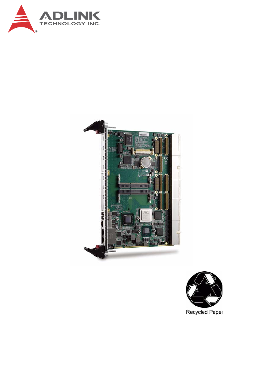
The cPCI-6870 Series is a 6U CompactPCI single board computer
in single slot (4HP) width form factor featuring a low power, small
form factor mobile Intel® chipset and supporting 45nm process
Core™2 Duo and Celeron® processors. The cPCI-6870 provides
up to 8GB dual channel DDR3-800/1066 memory capacity and
implements the Mobile Intel® GS45 Graphics and Memory Controller Hub and ICH9M-SFF I/O Controller Hub to provide a full
feature set and optimal performance.
The cPCI-6870 Series supports a 64bit/66MHz CompactPCI bus,
two PMC sites with 64-bit/66MHz PCI bus or two PCI-Express x8
XMC sites, four PCI-Express Gigabit Ethernet ports (two on front
panel, two for PICMG 2.16), a SAT A connector fo r an onboard 2.5”
SATA HDD, and CompactFlash socket support via the Rear Transition Module (RTM). For flexibility of use, the cPCI-6870 Series
can be installed in a standard CompactPCI system slot as system
master, or peripheral slot as a PCI device. The cPCI-6870 Series
is ideally suited for factory automation, transportation and military
applications.
cPCI-6870
Overview 1
Page 16

1.2 Features
X 6U CompactPCI SBC in 4HP width form factor
X µFC-BGA package Intel® CoreTM2 Duo or Celeron® proces-
sor, up to 2.26GHz
X 1066/800/667 MHz Front Side Bus depending on processor
X Mobile Intel® GS45 Memory Controller Hub and ICH9M-SFF
I/O Hub
X Dual Channel DDR3 non-ECC SDRAM at 800 or 1066MHz via
two SO-DIMM sockets, up to 8GB
X 64-bit/66MHz CompactPCI Interface based on PCI specifica-
tions, 3.3V and 5V signaling
X Supports operation in system slot as system master or in
peripheral slot with connectivity to CompactPCI bus (optional
isolation from CompactPCI bus)
X Dual PMC sites with 64-bit/133MHz PCI bus
X Dual XMC sites with PCI-Express x8 lane
X Four PCI-Express® Gigabit Ethernet ports , two at front, two for
PICMG 2.16
X Onboard CompactFlash socket
X 2.5” SATA HDD direct connector onboard, occupies outer
PMC/ XMC site
X Optional -20ºC to 70ºC extended temperature support
X RTM models available with multiple I/O options: SATA, HD
audio, COM, USB, Gigabit Ethernet, PS/2 KB/MS, PIM, SAS,
CF, SD socket
X Hardware RAID on SATA, SAS interfaces supported (depen-
dent on RTM module)
2Overview
Page 17
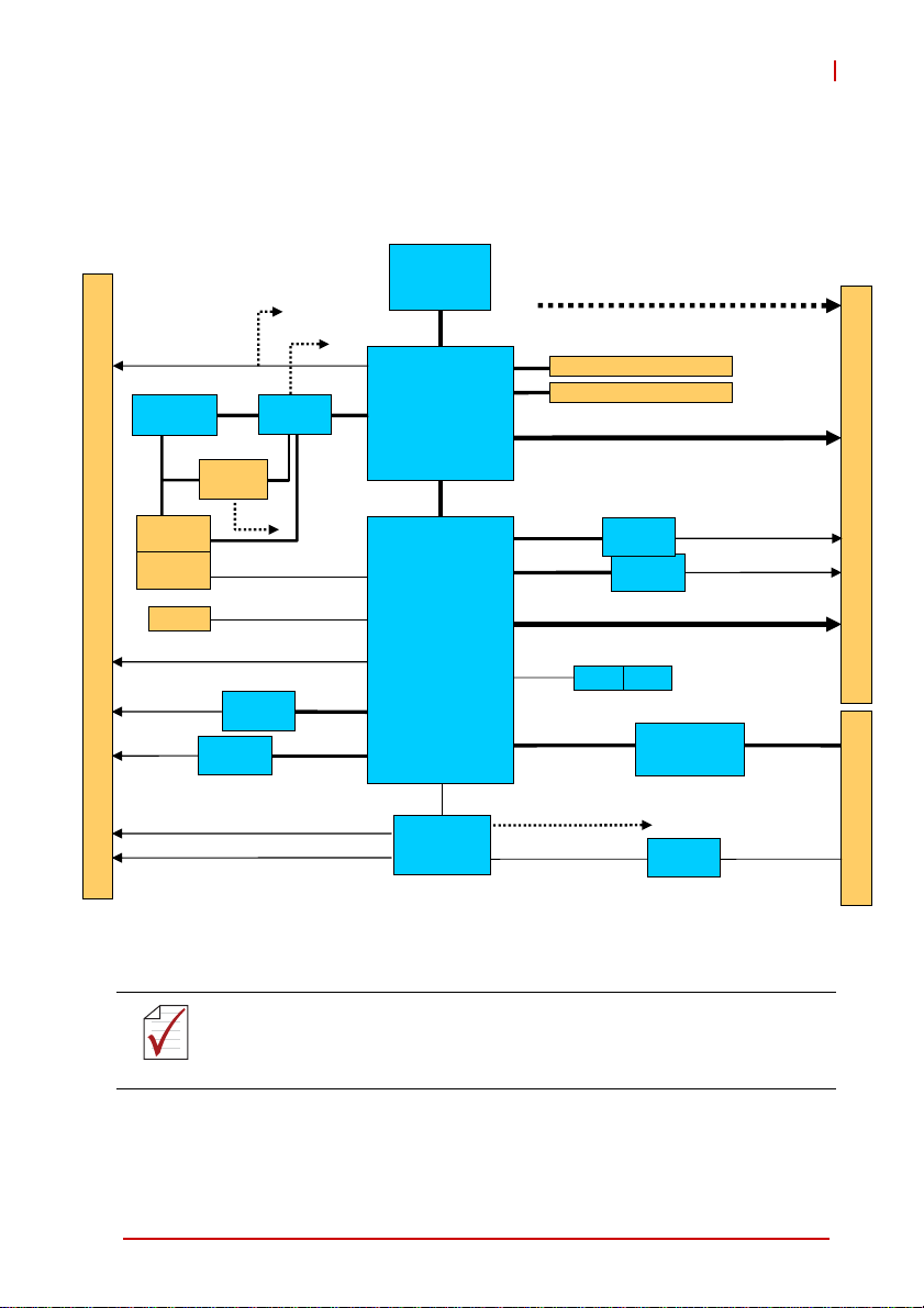
1.3 Block Diagram
VGA*
PCIe
CF
x4
PMC2/
XMC2
PIM
Intel
82574L
®
Intel
82574LL
SATA0
SATA1
F
R
O
N
T
P
A
N
E
L
PCIe to PCI
Bridge
PCI-X
64b/
133M
PMC1/
XMC1
2.5” SATA
HDD
USB1/2
GbE1
GbE2
COM1
Status LEDs
PCIe x4
PCIe
Switch
®
PCIe
x8
PCIe x1
PCIe x1
PCIe
x8
®
Intel
Core™2 Duo
®
Celeron
FSB 667/800/1066MHz
®
Intel
GS45
GMCH
®
Intel
ICH9M-SFF
Enhanced
LPC
Super I/O
ITE8783
VGA*, PS/2, COM3/4, FDD**, PIM, PCIe x4
DDR3 800/1066 SO-DIMM
DDR3 800/1066 SO-DIMM
LVD S
PCIe x1
PCIe x1
SATA2/3, USB (6x), HDA
SPI
BIOS
PCIe x2
KB/MS, FDD, COM3/4
COM2
Intel
82574L
Intel
82574L
BIOS
®
®
Pericom
PI7C9X130
IPMI
BMC
cPCI-6870
2.16 GbE (2x)
PCI
64b/66M
IPMB0/1
R
T
M
J2
J1
Figure 1-1: cPCI-6870 Series Block Diagram
*VGA is not supported on the front panel of models with ordering numbers
ending in “xx30” and higher. On these models, VGA is directly routed to the
NOTE:
NOTE:
RTM and the front panel RJ-45 connector is a dedicated serial port.
**Floppy support is not available on current model RTMs.
Overview 3
Page 18

1.4 Product List
Products included in the cPCI-6870 Series include:
Processor Blade
X cPCI-6870: 4HP width (single-slot) 6U CompactPCI blade fea-
turing single Intel® Core™2 Duo or Celeron® processor, dual
channel DDR3-800/1066 SDRAM via two SO-DIMM sockets,
two PMC/XMC sites, 2x USB, 2x GbE, RJ-45 COM/VGA*,
SATA, and CF socket
*VGA is not supported on the front panel RJ-45 connector of models with
ordering numbers ending in “xx30” and higher. On these models, VGA is
NOTE:
NOTE:
Rear Transition Modules
directly routed to the RTM and the RJ-45 connector is a dedicated serial port.
X cPCI-R6001P: 4HP width RTM with VGA, 2x COM, 3x USB,
2x GbE, PIM, SATA
X cPCI-R6002: 4HP width RTM with VGA, 2x COM, 3x USB,
2x GbE, SATA
X cPCI-R6002D: 8HP width RTM with VGA, 2x COM, 3x USB,
2x GbE, SATA, DB-R6000L2 riser card provides 2x USB,
KB/MS, Mic-in, Line-out and removable SATA direct connector (DB-6920SAT) for 2.5” SATA HDD
X cPCI-R6101: 4HP width RTM with 4x GbE, 4x USB, SATA,
VGA, PS/2 KB/MS, CF & SD sockets
X cPCI-R6111: 4HP width RTM with 2x GbE, 4x USB, SATA,
VGA, PS/2 KB/MS, CF, & SD sockets
X cPCI-R6201: 8HP width RTM with 2x GbE, 4x USB, 2x COM,
VGA, 2x SATA, Mic-in, Line-out, PS/2 KB/MS, 8x SAS
Adapter Kit
X DB-CF-SA: CompactFlash socket kit for cPCI-R6001D &
cPCI-R6201 RTMs, including DB-6920CF adapter board, car d
guide and screws to replace SA TA adapter with CompactFlash
socket
4Overview
Page 19

cPCI-6870
1.5 Package Contents
The cPCI-6870 is packaged with the components listed below
(RTMs and adapter kits are optional). If any of the items in the
contents list are missing or damaged, retain the shipping carton
and packing material and contact the dealer for inspection. Please
obtain authorization before returning any product to ADLINK. The
packing contents of non-standard configurations may vary
depending on customer requests.
Processor Blade
X The cPCI-6870 Series Processor Blade
Z CPU, RAM will differ depending on options selected
Z Thermal module is assembled on the board
X RJ-45 to DB-9 cable for RJ-45 COM port
X RJ-45 to DB-15 cable for RJ-45 VGA port
(
Not included with ordering numbers ending in “xx30” and higher.)
X DB-6920SAT SATA adapter card
X 2.5” SATA HDD mounting kit, including HDD bracket and
screws for HDD
X ADLINK All-in-One CD
X User’s manual
Rear Transition Module
X The cPCI-R6001P, cPCI-R6002(D)*, cPCI-R6101,
cPCI-R6111 or cPCI-R6201 RTM
*
Replaces cPCI-R6001(D).
X The DB-SATA kit (cPCI-R6002D, cPCI-R6111, cPCI-R6201
only)
X 2.5” HDD bracket (cPCI-R6002D, cPCI-R6201 only)
X Y-cable for PS/2 combo port (cPCI-R6002D, cPCI-R6101,
cPCI-R6111, cPCI-R6201 only)
X DVI to VGA (DB-15) adapter (cPCI-R6002, cPCI-R6001P,
cPCI-R6002D, cPCI-R6201 only)
Overview 5
Page 20
Adapter Kit
X The DB-CF-SA kit (for cPCI-R6002D, cPCI-R6201 RTM)
Z DB-6920CF adapter board
Z Screw pack
Z CF card guide
The contents of non-standard cPCI-6870 configurations may
vary depending on customer requests.
NOTE:
NOTE:
This product must be protected from static discharge and physical shock. Never remove any of the components except at a
CAUTION:
static-free workstation. Use the anti-static bag shipped with the
product when putting the board on a surface. Wear an
anti-static wrist strap properly grounded on one of the system's
ESD ground jacks when installing or servicing system components.
6Overview
Page 21

2 Specifications
2.1 cPCI-6870 SBC Specifications
PICMG® 2.0 CompactPCI® Rev. 3.0
CompactPCI
Standard
Mechanical
Processor
Chipset
Memory
CompactPCI Bus
PMC/XMC
Ethernet
PICMG® 2.1 Hot Swap Specification Rev.2.0
PICMG® 2.9 System Management Bus Rev. 1.0
PICMG® 2.16 Packet Switching Backplane Rev.1.0
Standard 6U CompactPCI®
Board size: 233.23 mm x 160mm
Single slot (4HP, 20.32mm) width
CompactPCI® connectors J1, J2, J3, J4 and J5 for cPCI-6870
µFC-BGA Intel® Core™2 Duo processor SP9300, 6MB L2 cache,
2.26GHz, 1066MHz FSB
µFC-BGA LV Intel® Core™2 Duo processor SL9400, 6MB L2
cache, 1.86GHz, 1066MHz FSB
µFC-BGA ULV Intel® Core™2 Duo processor SU9300, 3MB L2
cache, 1.2GHz, 800MHz FSB
µFC-BGA Intel® Celeron® processor ULV 723, 1MB L2 cache,
1.2GHz, 800MHz FSB
Intel® GS45 Graphics Memory Controller Hub (GMCH)
Intel® I/O Controller Hub 9M Enhanced (Intel ICH9M-Enhanced)
SFF
Dual channel DDR3-800/1066 SDRAM
Two SO-DIMM sockets
Maximum 8GB capacity
PCI 64-bit/ 66MHz; V(I/O) 3.3V and 5V signaling
Supports operation in system slot or in peripheral slot with
connectivity to CompactPCI bus (Universal Mode)
Two PCI 64-bit/133MHz PMC sites, V(I/O) 3.3V or 5V
Or two PCI-Express x8 XMC sites
Four PCI-Express® x1 Intel® 82574L GbE controllers
Two 10/100/1000BASE-T egress ports
Two 10/100/1000BASE-T ports on rear panel, optional PICMG
2.16 support by switch selection
cPCI-6870
Specifications 7
Page 22
Integrated in Intel® GS45 Express Chipset (GMCH)
Intel® Gen 5.0 integrated graphics engine
Intel® Dynamic Video Memory Technology (Intel® DVMT 5.0)
Graphics
Microsoft® Direct X 10 support
Analog RGB signal to front or rear by switch selection
VGA port on front panel via RJ-45 to DB-15 adapter cable3
(shared with RJ-45 COM port)
Analog RGB up to QXGA
Serial Ports
One 16C550 compatible RJ-45 RS-232 port on front panel
(shared with RJ-45 VGA port)
3
Two serial ports routed to rear I/O
Storage
Interfaces
2.5” SATA HDD direct connector onboard
CompactFlash Type II socket onboard
1
BIOS AMIBIOS®8, dual 16Mbit SPI flash memory, supports failover
Supports PICMG® 2.9 secondary system management bus
IPMI functions implemented as defined by IPMI Spec. v1.5;
IPMI Interface
ATmega128L-8AU Baseboard Management Controller (BMC)
with 128KB programmable in-system flash, 4KB EEPROM, and
4KB internal SDRAM
2x USB 2.0 ports
Faceplate I/O
2x 10/100/1000BASE-T Ethernet ports
RJ-45 serial port or VGA port
3
2x PMC/XMC slots
Onboard
Peripherals
Serial ATA connector (signal + power)
CompactFlash socket
Red Hat Enterprise 5.1 x86_64
Red Hat Enterprise Linux 5.1 i386
Microsoft® Windows® 7 x86 Edition
Microsoft® Windows® Server 2008 x64 Edition (Intel does not
provide INF and graphics driver)
Supported OS
Microsoft® Windows® Server 2003 32-bit Edition (Intel does not
provide graphics driver)
Microsoft® Windows® Vista x64 Edition (Intel does not provide
graphics driver)
Microsoft® Windows® XP Professional SP3 32-bit Edition
Microsoft® Windows® 2000 Professional SP4
Other OS support upon request
Operating
T emperature
Storage
Temperature
0ºC to 60ºC standard
1
-20ºC to 70ºC extended temperature (optional)
-40ºC to 85ºC
3
8 Specifications
Page 23

Humidity 20% to 95% non-condensing
Shock 15G peak-to-peak, 11ms duration, non-operating
Vibration
2
Operating: 2Grms. 5 to 500Hz, each axis (without HDD)
Compliance CE EN55022, FCC Class A
Notes:
1. ADLINK-certified th ermal design. The thermal performance is
dependent on the chassis cooling design. Forced airflow with
6 CFM is required to allow safe operation of the CPU at full
loading. Temperature limit of optional mass storage devices
may affect the thermal specification.
2. The hard drive limits the operational vibration tolerance. When
application requires higher specification for anti-vibration, it is
recommended to use a solid state drive (SSD) or Compact-
Flash card.
3. VGA is not supported on the front panel RJ-45 connector
(CN11) of models with ordering numbers ending in “xx30” and
higher. On these models, VGA is directly routed to the RTM
and the RJ-45 connector is a dedicated serial port.
Specifications are subject to change without prior notice.
cPCI-6870
NOTE:
NOTE:
Specifications 9
Page 24
2.2 I/O Connectivity Tables
Processor Blade
Function
cPCI-6870
Faceplate Board
Gigabit Ethernet 2—
COM1 1
(1)
(RJ-45) —
USB 2.0 2—
PMC/XMC —2
VGA 1
Serial ATA —1
(1)
(RJ-45) —
(2)
Compact Flash —1
Reset Button 1—
T able 2-1: SBC I/O Connectivity
Notes:
1. RJ-45 connector shared by COM port and VGA port. COM and
VGA cannot be used simultaneously. (VGA is not supported on the
front panel RJ-45 connector (CN11) of models with ordering numbers ending in “xx30” and higher.)
2. 2.5” HDD occupies the same space as the outer PMC/XMC
site and cannot be installed simultaneously.
10 Specifications
Page 25

RTMs
cPCI-6870
Function
cPCI-R6001P (4HP) cPCI-R6002 (4HP) cPCI-R6002D (8HP)
Faceplate Board Faceplate Board Faceplate Board
GbE 2—2— 2 —
USB 2.0 2 1 (5-pin) 2 1 (5-pin) 4 1 (5-pin)
COM 1(DB-9)
(1)
1
(10-pin)
1 (DB-9)
(1)
1
(10-pin)
1 (DB-9)
(1)
1
(10-pin)
VGA 1—1—1 —
PIM —1————
1
(2)
(2)
2
(opt.)
SATA — 1 (7-pin) — 1 (7-pin) —
CF —————
Mic-in ————1 —
Line-out ————1 —
PS/2 KB/
MS
————1 —
SD ————— —
SAS ————— —
Table 2-2: RTM I/O Connectivity (pt. 1)
Notes:
1. Tx, Rx signals only
2. One 7-pin signal connector for external HDD and one direct
connector for onboard 2.5” SATA HDD. Optional CompactFlash slot is supported by replacing SATA connector adapter
with CompactFlash adapter. SATA HDD and CF cannot be
used simultaneously.
Specifications 11
Page 26
RTMs (cont’d)
Function
cPCI-R6101 (4HP) cPCI-R6111 (4HP) cPCI-R6201 (8HP)
Faceplate Board Faceplate Board Faceplate Board
GbE 4—2 — 2—
USB 2.0 4 — 4 — 3 1 (5-pin)
(1)
COM 1 (RJ-45) — — — —
1
(10-pin)
VGA 1—1 — 1 —
PIM ——— — — —
SATA — 1 (7-pin) —
CF —
(5)
1
—
1 (for 2.5”
HDD)
(3)
1
—
—
1
(2)
(2)
2
(opt.)
Mic-in ——— — 1 —
Line-out ——— — 1 —
PS/2 KB/
MS
1—1 — 1 —
SD —1— 1 ——
SAS ——— —
4 (SFF-
8088)
4 (SFF-
8087)
Table 2-3: RTM I/O Connectivity (pt. 2)
Notes:
1. Tx, Rx signals only
2. One 7-pin signal connector for external HDD and one direct
connector for onboard 2.5” SATA HDD. Optional CompactFlash slot is supported by replacing SATA connector adapter
with CompactFlash adapter. SATA HDD and CF cannot be
used simultaneously.
3. Converted from USB
12 Specifications
Page 27

cPCI-6870
2.3 Power Requirements
In order to guarantee a stable functionality of the system, it is recommended to provide more power than the system requires. An
industrial power supply unit should be able to provide at least
twice as much power as the entire system requires of each
voltage. An ATX power supply unit should be able to provide at
least three times as much power as the entire system requires.
The tolerance of the voltage lines described in the CompactPCI
specification (PICMG 2.0 R3.0) is +5%/ -3% for 5, 3.3 V and ±5%
for ±12V. This specification is for power delivered to each slot an d
it includes both the power supply and the backplane tolerance.
Voltage
5V +5.0 VDC +5% / -3% 50 mV
3.3V +3.3 VDC +5% / -3% 50 mV
+12V +12 VDC +5% / -5% 240 mV
-12V -12 VDC +5% / -5% 240 mV
V I/O (PCI I/O
Buffer Voltage)
GND
Table 2-4: CompactPCI Input Voltage Characteristics
Nominal
Value
+3.3 VDC or
+5 VDC
Tolerance
+5% / -3% 50 mV
Max. Ripple
(P - P)
Specifications 13
Page 28
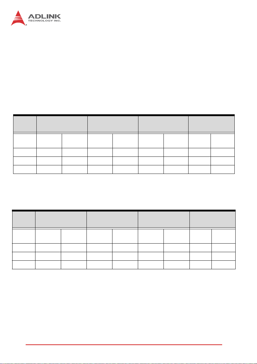
Power Consumption
This section provides information on the power consumption of
cPCI-6870 Series with different CPUs, 2GB soldered onboard
memory, 2x 2GB SO-DIMM memory, 100GB onboard SATA HDD
and cPCI-R6002 installed. The systems were tested in Idle Mode
and Full Load Mode under Windows XP running Burn-in Test 6.0.
The cPCI-6870 is powered by 5V, 3.3V and optional +12V.
Idle Mode under Windows XP
CPU
Voltage
(V)
+3.3 3.49 11.52 3.47 11.45 3.49 11.53 3.55 11.73
+5 5.32 26.61 3.12 15.60 3.14 15.71 3.41 17.08
Total 38.13 27.05 27.24 28.81
SV Core™2 Duo
SP9300
Current
(A)
Power
(W)
Table 2-5: Idle Mode Power Consumption
LV Core™2 Duo
SL9400
Current
(A)
Power
(W)
ULV Core™2 Duo
SU9300
Current
(A)
Power
(W)
ULV Celeron®
M 723
Current
(A)
Power
(W)
100% CPU Usage under Windows XP
CPU
Voltage
(V)
+3.3 3.46 11.44 3.47 11.45 3.49 11.53 3.55 11.73
+5 6.54 32.70 5.24 26.20 4.07 20.39 4.11 20.57
Total 44.14 37.65 31.93 32.30
SV Core™2 Duo
SP9300
Current
(A)
Power
(W)
T able 2-6: 100% CPU Usage Power Consumption
LV Core™2 Duo
SL9400
Current
(A)
Power
(W)
ULV Core™2 Duo
SU9300
Voltage
(A)
Current
(W)
ULV Celeron®
M 723
Power
Current
(A)
(W)
14 Specifications
Page 29

3 Functional Description
The following sections describe the cPCI-6870 Series features
and functions.
3.1 CPU
The following table lists the processors supported by the
cPCI-6870 Series and their power ratings.
cPCI-6870
Intel®
Features
Clock 2.26 GHz 1.86 GHz 1.2 GHz 1.2 GHz 1.2 GHz
L2 cache 6MB 6MB 3MB 1MB 1MB
FSB 1066MHz 1066MHz 800MHz 800MHz 800MHz
Max. Power (TDP1)
T
junction, MAX
Process 45nm 45nm 45nm 45nm 45nm
# of cores 2 2 2 1 1
2
Notes:
1. The high est expected sustainable power while running known
2. The maximum supported operating temperature.
Core™2 Duo
SP9300
25 W 17 W 10 W 5.5 W 10 W
105ºC 105ºC 105ºC 100ºC 100ºC
power intensive applications. TDP is not the maximum power
that the processor can dissipate.
Intel®
Core™2 Duo
SL9400
Intel®
Core™2 Duo
SU9300
Intel®
Celeron®
722
Intel®
Celeron®
723
Intel® Core™2 Duo Processor
The Intel® Core™2 Duo mobile processors are high-performance,
low-power processors based on the Intel® Core™ microarchitecture for Intel® Centrino® 2 technology. The following list outlines
the key features of this processor:
X Dual-core processor for mobile with enhanced performance
X Supports Intel architecture with Intel® Wide Dynamic Exe-
cution
X Supports L1 cache-to-cache (C2C) transfer
X On-die, primary 32-KB instruction cache and 32-KB,
write-back data cache in each core
Functional Description 15
Page 30

X The processor in DC-XE, standard voltage (SV) and LV
have an on-die, up to 6-MB second-level, share d cache with
Advanced Transfer Cache architecture
X The processor in ULV single-core and dual-core have an
on-die, up to 3-MB second-level, shared cache with
Advanced Transfer Cache architecture
X Streaming SIMD extensions 2 (SSE2), streaming SIMD
extensions 3 (SSE3), supplemental streaming SIMD extensions 3 (SSSE3) and SSE4.1 instruction sets
X The processor in DC-XE, SV and LV are offered at
1066-MHz, source-synchronous front side bus (FSB)
X Advanced power management features including Enhanced
Intel SpeedStep® Technology and dynamic FSB frequency
switching
X Digital thermal sensor (DTS)
X Intel® 64 architecture
X Supports enhanced Intel® Virtualization Technology
X Enhanced Intel® Dynamic Acceleration Technology and
Enhanced Multi-Threaded Thermal Management (EMTTM)
X Supports PSI2 functionality
X SV processor offered in Micro-FCPGA and Micro-FCBGA
packaging technologies
X Execute Disable Bit support for enhanced security
X Intel® Deep Power Down low-power state with P_LVL6 I/O
support
X Support for Intel® Trusted Execution Technology
X Half ratio support (N/2) for core to bus ratio
Intel® Celeron® Processor 722, 723
The Intel® Celeron® 722, 723 processor ar e based on 45 nm process
technology in small form factor (SFF). The following list provides
some of the key features of this processor:
X Single core with enhanced performance
X Ultra Low Voltage
X Supports L1 cache-to-cache transfer
16 Functional Description
Page 31

cPCI-6870
X On-die, primary 32-KB instruction cache and 32-KB
write-back data cache
X On-die, 1-MB second level shared cache with advanced
transfer cache architecture
X 800-MHz source-synchronous front side bus (FSB)
X Supports Intel® architecture with Intel® Wide Dynamic Execu-
tion
X Digital Thermal Sensor (DTS)
X 956-ball Micro-FCBGA packaging technology
X Execute Disable Bit support for enhanced securi ty
X Intel® 64 architecture (formerly Intel® EM64T)
X Architectural and performance enhancements of the Core
microarchitecture.
3.2 Chipset
The cPCI-6870 Series incorporates the Mobile Intel® 82GS45
Graphics and Memory Controller Hub (GMCH) and 82801IUX I/O
Controller Hub (ICH9M-SFF).
Intel® GS45 Graphics Memory Controller Hub
The following outlines the key features of GS45 GMCH.
Processor Support
X Intel® Core™2 Duo, Intel® Core™2 Solo, and Intel® Cel-
eron® mobile processors based on the 45-nm process
X 800-MHz and 1066-MHz FSBSupport for Dynamic FSB Fre-
quency Switching
X Support for Intel® Virtualization Technology (Intel® VT) for
Directed I/O (Intel® VT-d) (DMA)
X 36-bit interface to addressing, allowing the CPU to access
the entire 64 GB of the GMCH’s memory address space
Functional Description 17
Page 32

System Memory Support
X Supports DDR2 and DDR3 SDRAM (DDR3 only on
cPCI-6870)
X Support for DDR3 at 667, 800 and 1066 MHz
X Two Memory Channel Configurations supported in
Dual-channel Asymmetric
X 8-GB maximum memory support
X Support for x8 and x16 DDR2 and DDR3 devices
X 64-bit wide per channel
X No support for ECC
Direct Management Interface
X Chip-to-chip interface between GMCH and 82801
GMB/GHM
X Configurable as x2 or x4 DMI lanes
X 2-GB/s (1-GB/s each direction) point-to-point interface to ICH
X 32-bit downstream address
Integrated Graphics
X Intel Gen 5.0 integrated graphics engine with ten, fully-pro-
grammable cores
X 533-MHz core render clock @ 1.05-V core voltage
X Low-power configuration: 320-MHz core render clock at
1.05-V core voltage
X Supports HDMI/DVI, DP, TV-Out, LVDS, CRT and SDVO
(the cPCI-6870 implements analog CRT only)
X Intel® Dynamic Video Memory Technology (Intel® DVMT
5.0)
X Microsoft DirectX10 support
X Single channel LVDS interface support: 1x18 bpp
(LVDS signals are routed to J5 connector)
X Integrated 300-MHz DAC analog CRT
X Analog monitor support up to QXGA
X Support for CRT Hot-Plug
18 Functional Description
Page 33

cPCI-6870
Intel® ICH9M-SFF Mobile I/O Controller Hub
The ICH9M-SFF provides extensive I/O support. Functions and
capabilities include:
X ACPI Power Management Logic Support
X Integrated Serial ATA host controllers with independent
DMA operation on up to four ports and AHCI support.
Z Supports data transfer rates of up to 3.0 Gb/s (300
MB/s).
Z The SA T A controller con tains two modes of operation – a
legacy mode using I/O space, and an AHCI* mode using
memory space. Software that uses legacy mode will not
have AHCI* capabilities.
X Provides 6 PCI Express x1 ports, supporting the PCI
Express Base Specification, Revision 1.1. Each Root Port
supports 2.5GB/s bandwidth in each direction (5 GB/s concurrent). The cPCI-6870 utilizes four PCI Express ports 3-6
for four Gigabit Ethernet controllers and configures the PCI
Express ports 1-2 to PCI-Express x2 for connecting PCI
Express to PCI bridge to support 64bit/66MHz CompactPCI
bus..
X Enhanced DMA controller, interrupt controller, and timer
functions
X System Management Bus (SMBus) Specification, Version
2.0 with additional support for I2C devices
X Supports Intel® High Definition Audio
X Supports Intel® Virtualization Technology for Directed I/O
X PCI Local Bus Specification, Revision 2.3 support for
33MHz PCI operations
*
AHCI is a new programming interface for SATA host controllers. Platforms supporting AHCI may take advantage of performance features
such as no master/slave designation for SATA devices—each device
is treated as a master—and hardware-assisted native command
queuing. AHCI also provides usability enhancements such as
Hot-Plug. AHCI requires appropriate software support (e.g., an AHCI
driver) and for some features, hardware support in the SATA device or
additional platform hardware.
Functional Description 19
Page 34

3.3 Super I/O
The ITE IT8783F Super I/O is on a Low Pin Count interface supporting PS/2 keyboard/mouse, three 16C550-compatible serial
ports, floppy drive interface, hardware monitor function to monitor
CPU voltage, CPU temperature, power supply voltages and system
temperature, and Watch Dog Timer with time resolution from minimum 1 second or minute to maximum 65,535 seconds or minutes.
3.4 Battery
The cPCI-6870 is provided with a 3.0V coin cell lithium battery for
the Real Time Clock (RTC). The lithium battery must be replaced
with an identical battery or a battery type recommended by the
manufacturer. A Rayovac BR2032 is equipped on board by
default.
3.5 PMC/XMC Sites
The cPCI-6870 series supports two PMC sites for front panel I/O
expansion. The PMC sites provides a maximum 64bit/133MHz
PCI bus link using a Pericom PI7C9X130 PCI-Express-to-PCI
bridge and PCI-Express x4 link. The PMC site supports +3.3V or
+5V signaling.
The JN1/4 and JN2/5 connectors provide the signals for the 32-bit
PCI bus. The JN3/6 connector provides the 64 bit extension for the
PMC interface. The JN7 connector in PMC/XMC 2 supports user
defined I/O signals and is routed to the CompactPCI J4 connector
to rear I/O.
The cPCI-6870 provides two PCIe x8 XMC interfaces sharing
the same space as the PMC sites for high speed I/O e xpansion
such as 10GbE or high-end graphics.
20 Functional Description
Page 35

4 Board Interfaces
4.1 cPCI-6870 SBC Board Layout
cPCI-6870
CN9/10
CN11
CN12
CN3
U29
U39
CN7
CN8
U18
U3
U1
U5
CN4
U15
U26
SW4
CN2
U4
CN6
SW2 SW5
JN1
JN2
JN3
JN5
JN4 JN6
JN7
U16
U28
J5
J4
J3
J2
J1
SW3 SW1
SW6
SW13
SW12
SW8
SW7
U26 CPU CN3 SATA adapter card conn.
U18 North Bridge GS45 CN7/8 SO-DIMM socket
U3 South Bridge ICH9M-SFF CN9/10 USB ports
U16/28 PCIe to PCI Bridge CN11 COM/VGA port*
U4/5/29/39 Intel 82574L GbE controllers CN12 LAN ports
U15 PCIe Switch J1-J5 CompactPCI connectors
U1 Super I/O JN1-JN7 PMC connectors
CN2/6 XMC connectors SW1~13 Switches
CN4 CompactFlash socket SW4 Clear CMOS button
SW10
SW9
Figure 4-1: cPCI-6870 SBC Boar d La y out
*VGA is not supported on CN11 of models with ordering numbers ending in
“xx30” and higher. On these models, VGA is directly routed to the RTM and
NOTE:
NOTE:
the RJ-45 connector is a dedicated serial port.
Board Interfaces 21
Page 36

4.2 cPCI-6870 SBC Front Panel
GbE 1/2
PMC/XMC 1
PMC/XMC 2
Figure 4-2: cPCI-6870 Series Front Panel Layout
Status LEDs
HD WPTDWHW
LED Color Condition Indication
Power
(PW)
Hot Swap
(HW)
WDT
(WDT)
HDD
(HD)
Green
Blue
Red
Amber
OFF System is off
ON System is on
OFF Handles closed, System is on
Fast Blink
ON
Preparing to shut down system
(LED: 0.1s on, 0.9s off)
Handles open and SBC ready
to be removed
Voltages out of tolerance:
Slow Blink
3.3V, 5V , 12V, 1.5V over ±5%
(LED: 2s on, 1s off)
OFF No Watchdog event
ON Watchdog event alert
OFF No HDD activity
Blink Data read/write in process
COM/VGA*
2x USB 2.0
RST
Status LEDs
T able 4-1: cPCI-6870 Front Panel Status LED Descriptions
*
VGA is not supported on front panel RJ-45 of models with ordering numbers
ending in “xx30” and higher.
22 Board Interfaces
Page 37

4.3 Connector Pin Assignments
USB Connectors
Pin # Signal Name
1Vcc
2UV03UV0+
4GND
Table 4-2: USB Connector Pin Definition
RJ-45 COM/VGA* Port (CN-11)
Pin # COM Signal VGA Signal
1 DCD# DDCDAT_5V
2 RTS# HSYNC
3 DSR# VSYNC
4 TXD DDCCLK_5V
5RXD BLUE
6GND GND
7CTS# GREEN
8DTR# RED
cPCI-6870
1
6
Table 4-3: RJ-45 Serial/VGA Port Pin Definition
*VGA is not supported on CN11 of models with ordering numbers ending in
“xx30” and higher. On these models, VGA is directly routed to the RTM and
NOTE:
NOTE:
the RJ-45 connector is a dedicated serial port.
Board Interfaces 23
Page 38

PS/2 Keyboard/Mouse Connector (CN11-R)
Pin # Signal Function
1 KBDATA Keyboard Data
2MSDATA Mouse Data
3 GND Ground
4+5V Power
5 KBCLK Keyboard Clock
6 MSCLK Mouse Clock
Table 4-4: PS/2 Keyboard/Mouse Connector Pin Definition
RJ-45 Gigabit Ethernet Connectors (CN12, CN20-R, CN21-R)
Pin #
Network link is not established
10BASE-T/100BAS
E-TX
1 TX+ BI_DA+
2 TX- BI_DA3 RX+ BI_DB+
4 -- BI_DC+
5-- BI_DC6 RX- BI_DB7 -- BI_DD+
8-- BI_DD-
Ta ble 4-5: GbE Connector Pin Definitions
Status (CN4, CN5)
or system powered off
10 Mbps
100 Mbps
1000 Mbps
Link OFF ON
Active OFF Blinking
Link Green ON
Active Green Blinking
Link Amber ON
Active Amber Blinking
1000BASE-T
Speed LED
(Green/Amber)
OFF OFF
1
Activity LED
(Amber)
8
Table 4-6: GbE LED CN12 Status Definitions
24 Board Interfaces
Page 39

DB-9 Serial Port (CN9-R)
Pin # RS-232
1 DCD, Data carrier detect
2 RXD, Receive data
3TXD, Transmit data
4 DTR, Data terminal ready
5 IsoGND, Isolated ground
6 DSR, Data set ready
7 RTS, Request to send
8 CTS, Clear to send
9 RI, Ring indicator
Table 4-7: COM1-2 Serial Port Connector Pin Definition
Onboard Serial Port Connector (CN10-R)
Pin # RS-232
1 Not used
2 Not used
3 RXD, Receive data
4 Not used
5 TXD, Transmit data
6 Not used
7 Not used
8 Not used
9 IsoGND, Isolated ground
10 Not used
12
910
cPCI-6870
Table 4-8: Onboard Serial Port Connector Pin Definition
Board Interfaces 25
Page 40

Serial ATA Connectors (CN1-R)
Pin # Signal
1GND
2TX+
3TX4GND
5RX6RX+
7GND
Table 4-9: SATA Connector Pin Definition
Serial ATA Connector on DB-6920SAT
Pin # Signal
S1 GND
S2 TX+
S3 TXS4 GND
S5 RXS6 RX+
S7 GND
P1 NC
P2 NC
P3 NC
P4 GND
P5 GND
P6 GND
P7 5V
P8 5V
P9 5V
P10 GND
P11 Reserved
P12 GND
P13~P15 12V
1
7
S1
Signal
S7
P1
Power
P15
Table 4-10: DB-6920SAT SATA Connector Pin Definition
26 Board Interfaces
Page 41

PMC Connector (JN1/4, JN2/5, JN3/6, JN7)
cPCI-6870
Pin# JN1/4 Signal JN2/5 Signal JN3/6 Signal JN7 Signal
1 PMC_TCK P12V NC PIO1
2 N12V PMC_TRST-L GND PIO2
3 GND PMC_TMS GND PIO3
4 PCIX_INTA-L NC (PMC_TDO) PCIX_CBE-L7 PIO4
5 PCIX_INTB-L PMC_TDI PCIX_CBE-L6 PIO5
6 PCIX_INTC-L GND PCIX_CBE-L5 PIO6
7 PMC_MOD-L1 GND PCIX_CBE-L4 PIO7
8P5V NC GNDPIO8
9 PCIX_INTD-L NC PMC_VIO PIO9
10 NC NC PCIX_PAR64 PIO10
11 GND PMC_MOD-L2 PCIX_AD63 PIO11
12 P3V3_PMCAUX P3V3 PCIX_AD62 PIO12
13 CLK66_PCIX_PMC PMC_RST-L PCIX_AD61 PIO13
14 GND PMC_MOD-L3 GND PIO14
15 GND P3V3 GND PIO15
16 PCIX_GNT-L0 PMC_MOD-L4 PCIX_AD60 PIO16
17 PCIX_REQ-L0 PMC_PME-L PCIX_AD59 PIO17
18 P5V GND PCIX_AD58 PIO18
19 PMC_VIO PCIX_AD30 PCIX_AD57 PIO19
20 PCIX_AD31 PCIX_AD29 GND PIO20
21 PCIX_AD28 GND GND PIO21
22 PCIX_AD27 PCIX_AD26 PCIX_AD56 PIO22
23 PCIX_AD25 PCIX_AD24 PCIX_AD55 PIO23
24 GND PCIX_AD23 PCIX_AD54 PIO24
25 GND PMC_IDSEL PCIX_AD53 PIO25
26 PCIX_CBE-L3 PCIX_AD23 GND PIO26
27 PCIX_AD22 P3V3 GND PIO27
28 PCIX_AD21 PCIX_AD20 PCIX_AD52 PIO28
29 PCIX_AD19 PCIX_AD18 PCIX_AD51 PIO29
30 P5V GND PCIX_AD50 PIO30
31 PCIX_FRAME-L PCIX_AD16 PCIX_AD49 PIO31
32 PCIX_AD17 PCIX_CBE-L2 GND PIO32
6364
12
Table 4-11: PMC Connector Pin Definitions
Board Interfaces 27
Page 42

Pin# JN1/4 Signal JN2/5 Signal JN3/6 Signal JN7 Sig nal
33 PCIX_FRAME-L GND GND PIO33
34 GND NC PCIX_AD48 PIO34
35 GND PCIX_TRDY-L PCIX_AD47 PIO35
36 PCIX_IRDY-L P3V3 PCIX_AD46 PIO36
37 PCIX_DEVSEL-L GND PCIX_AD45 PIO37
38 P5V PCIX_STOP-L GND PIO38
39 PCIX_PCIXCAP PCIX_PERR-L GND PIO39
40 PCIX_LOCK-L GND PCIX_AD44 PIO40
41 NC P3V3 PCIX_AD43 PIO41
42 NC PCIX_SERR-L PCIX_AD42 PIO42
43 PCIX_PAR PCIX_CBE-L1 PCIX_AD41 PIO43
44 GND GND GND PIO44
45 PMC_VIO PCIX_AD14 GND PIO45
46 PCIX_AD15 PCIX_AD13 PCIX_AD40 PIO46
47 PCIX_AD12 PCIX_M66EN PCIX_AD39 PIO47
48 PCIX_AD11 PCIX_AD10 PCIX_AD38 PIO48
49 PCIX_AD9 PCIX_AD8 PCIX_AD37 PIO49
50 P5V P3V3 GND PIO50
51 GND PCIX_AD7 GND PIO51
52 PCIX_CBE-L0 NC PCIX_AD36 PIO52
53 PCIX_AD6 P3V3 PCIX_AD35 PI O53
54 PCIX_AD5 NC PCIX_AD34 PIO54
55 PCIX_AD4 NC PCIX_AD33 PIO55
56 GND GND GND PIO56
57 PMC_VIO NC GND PIO57
58 PCIX_AD3 NC PCIX_AD32 PIO58
59 PCIX_AD2 GND NC PIO59
60 PCIX_AD1 NC NC PIO60
61 PCIX_AD0 PCIX_ACK64-L NC PIO61
62 P5V P3V3 GND PIO62
63 GND GND GND PIO63
64 PCIX_REQ64-L NC NC PIO64
Table 4-11: PMC Connector Pin Definitions (cont’d)
28 Board Interfaces
Page 43

cPCI-6870
XMC Connectors (CN2, CN6)
Pin# A B C D E F
1 PETp0 PETn0 3.3V PETp1 PETn1 VPWR
2 GND GND TRST# GND GND MRSTI#
3 PETp2 PETn2 3.3V PETp3 PETn3 VPWR
4 GND GND TCK GND GND MRSTO#
5 PETp4 PETn4 3.3V PETp5 PETn5 VPWR
6 GND GND TMS GND GND +12V
7 PETp6 PETn6 3.3V PETp7 PETn7 VPWR
8 GND GND TDI GND GND -12V
9NC NCNCNCNCVPWR
10 GND GND TDO GND GND GA0
11 PERp0 PERn0 MBIST# PERp1 PERn1 VPWR
12 GND GND GA1 GND GND MPRESENT#
13 PERp2 PERn2 3.3V AUX PERp3 PERn3 VPWR
14 GND GND GA2 GND GND MSDA
15 PERp4 PERn4 NC PERp5 PERn5 VPWR
16 GND GND MVMRO GND GND MSCL
17 PERp6 PERn6 NC PERp7 PERn7 NC
18 GND GND NC GND GND NC
19 REFCLK+0 REFCLK-0 NC WAKE# ROOT0# NC
Table 4-12: XMC Connector Pin Definition
Board Interfaces 29
Page 44

68-pin SCSI Connector (CN12-R)*
Signal Pin # Pin # Signal
SCSI-SDP12 1 35 SCSI-SDN12
SCSI-SDP13 2 36 SCSI-SDN13
SCSI-SDP14 3 37 SCSI-SDN14
SCSI-SDP15 4 38 SCSI-SDN15
SCSI-SDP1-P1 5 39 SCSI-SDP1-N1
SCSI-SDP0 6 40 SCSI-SDN0
SCSI-SDP1 7 41 SCSI-SDN1
SCSI-SDP2 8 42 SCSI-SDN2
SCSI-SDP3 9 43 SCSI-SDN3
SCSI-SDP4 10 44 SCSI-SDN4
SCSI-SDP5 11 45 SCSI-SDN5
SCSI-SDP6 12 46 SCSI-SDN6
SCSI-SDP7 13 47 SCSI-SDN7
SCSI-SDP0-P0 14 48 SCSI-SDP0-N0
GND 15 49 GND
DIFFSEN 16 50 NC
P3V3_SCSI 17 51 P3V3_SCSI
P3V3_SCSI 18 52 P3V3_SCSI
NC 19 53 NC
GND 20 54 GND
SCSI-SATN-P 21 55 SCSI-SATN-N
GND 22 56 GND
SCSI-SBSY-P 23 57 SCSI-SBSY-N
SCSI-SACK-P 24 58 SCSI-SACK-N
SCSI-SRST-P 25 59 SCSI-SRST-N
SCSI-SMSG-P 26 60 SCSI-SMSG-N
SCSI-SSEL-P 27 61 SCSI-SSEL-N
SCSI-SCD-P 28 62 SCSI-SCD-N
SCSI-SREQ-P 29 63 SCSI-SREQ-N
SCSI-SIO-P 30 64 SCSI-SIO-N
SCSI-SDP8 31 65 SCSI-SDN8
SCSI-SDP9 32 66 SCSI-SDN9
SCSI-SDP10 33 67 SCSI-SDN10
SCSI-SDP11 34 68 SCSI-SDN11
1
34
35
68
Table 4-13: 68-pin SCSI Connector Pin Definition
30 Board Interfaces
Page 45

Floppy Connector 34-pin (CN4-R)*
Pin # Signal Pin # Signal
1 GND 2 Extended Density
3 GND 4 No Connect
5 NC 6 Data Rate
7 GND 8 Index
9 GND 10 Motor A Select
11 GND 12 Drive B Select
13 GND 14 Drive A Select
15 GND 16 Motor B Select
17 GND 18 Step Direction
19 GND 20 Step Pulse
21 GND 22 Write Data
23 GND 24 Write Gate
25 GND 26 Track 0
27 GND 28 Write Protect
29 GND 30 Read Data
31 GND 32 Side 1
33 GND 34 Disk Change
cPCI-6870
Table 4-14: Floppy Connector Pin Definition
*SCSI and floppy are not supported on current model RTMs. These pin defini-
tions are provided for customers with older model RTMs.
NOTE:
NOTE:
Board Interfaces 31
Page 46

PIM Connector (JN1-R)
Pin# Signal Name Signal Name Pin#
1 PIM1 PIM2 2
3 PIM3 PIM4 4
5 PIM5 PIM6 6
7 PIM7 PIM8 8
9 PIM9 PIM10 10
11 PIM11 PIM12 12
13 PIM13 PIM14 14
15 PIM15 PIM16 16
17 PIM17 PIM18 18
19 PIM19 PIM20 20
21 PIM21 PIM22 22
23 PIM23 PIM24 24
25 PIM25 PIM26 26
27 PIM27 PIM28 28
29 PIM29 PIM30 30
31 PIM31 PIM32 32
33 PIM33 PIM34 34
35 PIM35 PIM36 36
37 PIM37 PIM38 38
39 PIM39 PIM40 40
41 PIM41 PIM42 42
43 PIM43 PIM44 44
45 PIM45 PIM46 46
47 PIM47 PIM48 48
49 PIM49 PIM50 50
51 PIM51 PIM52 52
53 PIM53 PIM54 54
55 PIM55 PIM56 56
57 PIM57 PIM58 58
59 PIM59 PIM60 60
61 PIM61 PIM62 62
63 PIM63 PIM64 64
6364
12
Table 4-15: PIM Connector (JN1-R) Pin Definition
32 Board Interfaces
Page 47

PIM Connector (JN2-R)
cPCI-6870
Pin# Signal Name Signal Name Pin#
1NC NC 2
3NC NC 4
5P5V NC 6
7NC NC 8
9NC P3V310
11 NC NC 12
13 GND NC 14
15 NC NC 16
17 NC GND 18
19 NC NC 20
21 P5V NC 22
23 NC NC 24
25 NC P3V3 26
27 NC NC 28
29 GND NC 30
31 NC NC 32
33 NC GND 34
35 NC NC 36
37 P5V NC 38
39 NC NC 40
41 NC P3V3 42
43 NC NC 44
45 GND NC 46
47 NC NC 48
49 NC GND 50
51 NC NC 52
53 P5V NC 54
55 NC NC 56
57 NC P3V3 58
59 NC NC 60
61 NC NC 62
63 NC NC 64
6364
12
Table 4-16: PIM Connector (JN2-R) Pin Definition
Board Interfaces 33
Page 48

CompactFlash Connector
Signal Name Pin# Pin# Signal Name
GND 1 26 GND
DD3 2 27 DD11
DD4 3 28 DD12
DD5 4 29 DD13
DD6 5 30 DD14
DD7 6 31 DD15
CS1J 7 32 CS3J
GND 8 33 GND
GND 9 34 SDIORJ
GND 10 35 SDIOWJ
GND 11 36 5V
GND 12 37 IRQ15
5V 13 38 5V
GND 14 39 PCSEL
GND 15 40 NC
GND 16 41 BRSTDRVJ
GND 17 42 SDIORDY
DA2 18 43 NC
DA1 19 44 SDACKJ
DA0 20 45 IDEACTJ
DD0 21 46 DIAG
DD1 22 47 DD8
DD2 23 48 DD9
IOIS16J 24 49 DD10
GND 25 50 GND
Table 4-17: CompactFlash Connector Pin Definition
34 Board Interfaces
Page 49

DB-6920SAT/CF Connector (CN3, CN6-R)
cPCI-6870
Signal Name Pin # Pin # Signal Name
GND 1 2 GND
GND 3 4 GND
GND 5 6 GND
GND 7 8 GND
GND 9 10 GND
GND 11 12 GND
GND 13 14 GND
GND 15 16 GND
GND 17 18 GND
GND 19 20 GND
GND 21 22 GND
GND 23 24 GND
GND 25 26 GND
GND 27 28 GND
GND 29 30 GND
P3V3 31 32 P5V
P3V3 33 34 P5V
P3V3 35 36 P5V
P3V3 37 38 P5V
P1V8 39 40 NC
P1V8 41 42 NC
P1V8 43 44 NC
GND 45 46 GND
GND 47 48 SATA-TXN0
GND 49 50 SATA-TXP0
SATA-RXN0 51 52 GND
SATA-RXP0 53 54 GND
GND 55 56 RESET#
GND 57 58 GND
GND 59 60 GND
1 2
59 60
Table 4-18: DB-6920SAT/CF Connector Pin Definition
Board Interfaces 35
Page 50

DB-R6000L2 Connector (CN14-R)
Signal Name Pin # Pin # Signal Name
SATA-T1P 1 2 USB-P3
SATA-T1N 3 4 USB-N3
GND 5 6 GND
SATA-R1P 7 8 USB-OC3#
SATA-R1N 9 10 GND
GND 11 12 GND
GND 13 14 USB-P2
HAD_RST-L 15 16 USB-N2
HAD_SYNC 17 18 GND
HAD_SDOUT 19 20 USB-OC2#
HAD_BIT_CLK 21 22 GND
HAD_SDIN0 23 24 PS2-KBC
GND 25 26 PS2-KBD
HAD_SDIN1 27 28 PS2-MSD
HAD_SDIN2 29 30 PS2-MSC
HAD_SDIN3 31 32 GND
GND 33 34 RESET#
GND 35 36 GND
GND 37 38 GND
GND 39 40 GND
GND 41 42 GND
GND 43 44 GND
GND 45 46 GND
GND 47 48 GND
GND 49 50 GND
P5V 51 52 P1V8
P5V 53 54 P1V8
P5V 55 56 P1V8
P5V 57 58 NC
P5V 59 60 NC
GND 61 62 GND
60
12
61
62
59
Table 4-19: DB-R6000L2 Connector Pin Definition
36 Board Interfaces
Page 51

cPCI-6870
CompactPCI J1 Connector Pin Assignment
Pin Z A B C D E F
1 GND +5V -12V TRST# +12V +5V GND
2 GND TCK# +5V TMS# NC TDI# GND
3 GND IRQA# IRQB# IRQC# +5V IRQD# GND
4 GND +5V_IPMB HEALTHY# V(I/O) NC NC GND
5 GND NC NC RESET# GND GNT0# GND
6 GND REQ0# GND +3.3V CLK0 AD31 GND
7 GND AD30 AD29 AD28 GND AD27 GND
8 GND AD26 GND V(I/O) AD25 AD24 GND
9 GND CBE3# IDSEL AD23 GND AD22 G ND
10 GND AD21 GND +3.3V AD20 AD19 GND
11 GND AD18 AD17 AD16 GND CBE2# GND
12-14 Key
15 GND +3.3V FRAME# IRDY# BDSEL# TRDY# GND
16 GND DEVSEL# PCIXCAP V(I/O) STOP# LOCK# GND
17 GND +3.3V IPMB_CLK IPMB_DAT GND PERR# GND
18 GND SERR# GND +3.3V PAR CBE1# GND
19 GND +3.3V AD15 AD14 GND AD13 GND
20 GND AD12 GND VIO AD11 AD10 GND
21 GND +3.3V AD9 AD8 M66EN CBE0# GND
22 GND AD7 GND +3.3V AD6 AD5 GND
23 GND +3.3V AD4 AD3 +5V AD2 GND
24 GND AD1 +5V V(I/O) AD0 ACK64# GND
25 GND +5V REQ64# ENUM# +3.3V +5V GND
Ta ble 4-20: CompactPCI J1 Connecto r Pin De fini tion
Board Interfaces 37
Page 52

CompactPCI J2 Connector Pin Assignment
Pin Z A B C D E F
1 GND CLK1 GND REQ1# GNT1# REQ2# GND
2 GND CLK2 CLK3 SYSEN# GNT2# REQ3# GND
3 GND CLK4 GND GNT3# REQ4# GNT4# GND
4 GND V(I/O) NC CBE7# GND CBE6# GND
5 GND CBE5# GND V(I/O) CBE4# PAR64 GND
6 GND AD63 AD62 AD61 GND AD60 GND
7 GND AD59 GND V(I/O) AD58 AD57 GND
8 GND AD56 AD55 AD54 GND AD53 GND
9 GND AD52 GND V(I/O) AD51 AD50 GND
10 GND AD49 AD48 AD47 GND AD46 GND
11 GND AD45 GND V(I/O) AD44 AD43 GND
12 GND AD42 AD41 AD40 GND AD39 GND
13 GND AD38 GND V(I/O) AD37 AD36 GND
14 GND AD35 AD34 AD33 GND AD32 GND
15 GND NC GND FAL# REQ5# GNT5# GND
16 GND NC NC DEG# GND NC GND
17 GND NC GND RSTBTN# REQ6# GNT6# GND
18 GND NC NC NC GND NC GND
19 GND GND GND NC NC NC GND
20 GND CLK5 GND NC GND NC GND
21 GND CLK6 GND NC NC NC GND
22 GND GA4 GA3 GA2 GA1 GA0 GND
Table 4-21: CompactPCI J2 Connector Pin Definition
38 Board Interfaces
Page 53

cPCI-6870
CompactPCI J3 Pin Assignment
Pin Z A B C D E F
1GNDHDA_RST# HDA_SYNC HDA_BIT_CLK HDA_SDOUT HDA_SDIN0 GND
2GND
3GND
4GND
5 GND GND GND NC GND GND GND
6GND
7GND
8GND
9GND
10 GND
11 GND
12 GND
13 GND
14 GND
15 GND
16 GND
17 GND
18 GND
19 GND P5V P5V P12V P5V P5V GND
HDA_SDIN1 HDA_SDIN2 NC
KBDATA KBCLK NC MSDATA MSCLK GND
SATA-TX3+ SATA-TX3- GND SATA-TX2+ SATA-TX2- GND
SATA-RX3+ SATA-RX3- GND SATA-RX2+ SATA-RX2- GND
COM4-TX COM4-RX COM3-DCD# IPMB_CLK IPMB_DAT GND
COM3-RX COM3-TX COM3-DTR# COM3-DSR# COM3-RTS# GND
COM3-CTS# COM3-RI# RGB-BLUE RGB-RED RGB-GREEN GND
USB-OC3# RGB-DDCCLK RGB-DDCDAT RGB-HSYNC RGB-VSYNC GND
USB-P3+ USB-P3- GND USB-P4+ USB-P4- GND
USB-P5+ USB-P5- GND USB-P6+ USB-P6- GND
USB-P7+ USB-P7- GND USB-P8+ USB-P8- GND
USB-OC4# USB-OC5# USB-OC6# USB-OC7# USB-OC8# GND
LAND_TXD1+ LAND_TXD1- GND LAND_TXD3+ LAND_TXD3- GND
LAND_TXD0+ LAND_TXD0- GND LAND_TXD2+ LAND_TXD2- GND
LANC_TXD1+ LANC_TXD1- GND LANC_TXD3+ LANC_TXD3- GND
LANC_TXD1+ LANC_TXD0- GND LANC_TXD2+ LANC_TXD2- GND
HDA_DOCK_EN#
HAD_DOCK_RST#
GND
Ta ble 4-22: CompactPCI J3 Connecto r Pin De fini tion
High Definition audio
Keyboard/Mouse
Serial ATA
Serial ports
USB ports
Ethernet ports
RGB
Board Interfaces 39
Page 54

CompactPCI J4 Connector Pin Assignment
Pin Z A B C D E F
1 GND PMC IO:61 PMC IO:63 NC PMC IO:62 PMC IO:64 GND
2 GND PMC IO:57 PMC IO:59 NC PMC IO:58 PMC IO:60 GND
3 GND NC NC NC NC NC GND
4 GND PMC IO:53 PMC IO:55 NC PMC IO:54 PMC IO:56 GND
5 GND PMC IO:49 PMC IO:51 NC PMC IO:50 PMC IO:52 GND
6 GND NC NC NC NC NC GND
7 GND PMC IO:45 PMC IO:47 NC PMC IO:46 PMC IO:48 GND
8 GND PMC IO:41 PMC IO:43 NC PMC IO:42 PMC IO:44 GND
9 GND NC NC NC NC NC GND
10 GND PMC IO:37 PMC IO:39 NC PMC IO:38 PMC IO:40 GND
11 GND PMC IO:33 PMC IO:35 NC PMC IO:34 PMC IO:36 GND
12-14 Key
15 GND PMC IO:29 PMC IO:31 NC PMC IO:30 PMC IO:32 GND
16 GND PMC IO:25 PMC IO:27 NC PMC IO:26 PMC IO:28 GND
17 GND NC NC NC NC NC GND
18 GND PMC IO:21 PMC IO:23 NC PMC IO:22 PMC IO:24 GND
19 GND PMC IO:17 PMC IO:19 NC PMC IO:18 PMC IO:20 GND
20 GND NC NC NC NC NC GND
21 GND PMC IO:13 PMC IO:15 NC PMC IO:14 PMC IO:16 GND
22 GND PMC IO:9 PMC IO:11 NC PMC IO:10 PMC IO:12 GND
23 GND NC NC NC NC NC GND
24 GND PMC IO:5 PMC IO:7 NC PMC IO:6 PMC IO:8 GND
25 GND PMC IO:1 PMC IO:3 NC PMC IO:2 PMC IO:4 GND
Table 4-23: CompactPCI J4 Connector Pin Definition
40 Board Interfaces
Page 55

cPCI-6870
CompactPCI J5 Pin Assignment
Pin Z A B C D E F
1GNDPCIE-TX0+ PCIE-TX0+ GND PCIE-RX0+ PCIE-RX0- GND
2GND
3GND
4GND
5 GND GND GND GND GND GND GND
6GND
7 GND GND GND RTC GND GND GND
8GND
9GND
10 GND NC NC GND NC NC GND
11 GND NC NC GND NC NC GND
12 GND NC NC NC NC NC GND
13 GND
14 GND NC NC GND NC NC GND
15 GND NC NC
16 GND
17 GND
18 GND
19 GND
20 GND
21 GND
22 GND NC
PCIE-TX1+ PCIE-TX1- GND PCIE-RX1+ PCIE-RX1- GND
PCIE-TX2+ PCIE-TX2- GND PCIE-RX2+ PCIE-RX2- GND
PCIE-TX3+ PCIE-TX3- GND PCIE-RX3+ PCIE-RX3- GND
PCIE-CLK+ PCIE-CLK- GND RESET# RTM_IN# GND
LVDS_DATA3- LVDS_DATA3+ NC LVDS_CLK LVDS_DATA GND
GPIO1 GPIO2 GPIO3 GPIO4 GPIO5 GND
LAND_100# LANC_100# NC LANC_1G# LAND_1G# GND
GPIO6 NC NC GND
MTR0# INDEX# GPIO7 NC DENSEL# GND
DIR# NC GPIO8 DRVA# NC GND
TRK0# WGATE# DETECT# WDATA# STEP# GND
DSKCHG# HDSEL# NC RDATA# WRPORT# GND
LVDS_DATA0- LVDS_DATA0+ GND LVDS_DATA1- LVDS_DATA1+ GND
LVDS_DATA2- LVDS_DATA2+ GND LVDS_CLK- LVDS_CLD+ GND
LAND_LINK_ACT#
+3.3V
LANC_LINK_ACT#
+3.3V GND
Ta ble 4-24: CompactPCI J5 Connecto r Pin De fini tion
PCI-Express x4
GPIO
Floppy
Ethernet port
LVDS
Board Interfaces 41
Page 56

4.4 Switch and Jumper Settings
Mode Switch (SW2)
Switch SW2 is a multi purpose switch that allows users to
define the board operating mode. Four pins independ ently control the mode setting. All are set to OFF by default.
Pin# Status Description
Universal Mode: The cPCI-6870 in a peripheral slot has
CompactPCI bus communication with the host board in the system
OFF
slot. The cPCI-6870 can boot-up in a peripheral slot and be
1
2
3
4
recognized by the host board in the system slot as a PCI device.
Satellite Mode: The cPCI-6870 in a peripheral slot has no
CompactPCI bus communication with the host board in the system
ON
slot. The cPCI-6870 behaves a as standalone blade in the
peripheral slot.
When the system does not include a CMM (Chassis
OFF
Management
"without CMM mode".
When the system includes a CMM, set this pin to ON to allow
ON
IPMI to run in "with CMM mode".
The cPCI-6870 cannot boot-up when installed in a peripheral slot if
OFF
there is no host board in the system slot.
The cPCI-6870 is able to boot-up when installed in a peripheral
slot if there is no host board in the system slot. The cPCI-6870
ON
behaves as a system board in all slots. (Set this pin to "ON" if the
cPCI-6870 is installed in a blade server backplane).
The cPCI-6870 power on/off state is controlled by the ejector
OFF
handle state.
ON
Force the ejector handle state to "closed".
Table 4-25: Mode Switch Settings
Module), set this pin to OFF to allow IPMI to run in
42 Board Interfaces
Page 57

cPCI-6870
Clear CMOS Switch (SW4)
Press switch SW4 to clear the CMOS and reset the CMOS values to default.
PMC Clock Switch (SW1)
Switch SW1 sets the PCI bus clock of the two PMC sites. All
are set OFF by default.
Mode 1 2 3 4
PCI-X 133MHz OFF OFF OFF OFF
PCI-X 100MHz OFF OFF OFF ON
PCI-X 66MHz OFF OFF ON OFF
PCI 66MHz ONONONOFF
PCI 33MHz ON OFF ON OFF
Table 4-26: PMC Clock Switch Settings
PMC V(I/O) Switch (SW5)
Switch SW5 sets the signaling voltage of the two PMC sites.
Mode 1 2 3 4
PMC V(I/O) = 5V ON ON OFF OFF
PMC V(I/O) = 3.3V OFF OFF ON ON
Table 4-27: PMC V(I/O) Switch Settings
Board Interfaces 43
Page 58

COM1/Debug Switch (SW9, SW10 pins 1-2)
Switches SW9 and SW10 (pins 1, 2) set the RJ-45 serial port (CN11)
as a standard RS-232 serial port or as an IPMI debugging port
SW9 SW10
.
Mode
1 2 3 4 1 2
RS-232 COM port (default) ON ON OFF OFF ON OFF
IPMI debugging port OFF OFF ON ON OFF ON
Table 4-28: COM1/Debug Switch Settings
SW9 SW10
Front/Rear VGA Selection Switch (SW10 pins 3-4)*
Switch SW10 (pins 3, 4) sets the VGA output to the front panel
RJ-45 port (CN11) or the VGA port on the RTM. The default
VGA output is set to rear I/O. To enable Front VGA output, the
COM/VGA Mode Selection Switches (SW7-8, SW12-13)*
must be set to VGA mode.
Mode 3 4
Rear VGA output (default) ON OFF
Front VGA output OFF ON
Table 4-29: Front/Rear VGA Selection Switch Settings
*VGA is not supported the front panel RJ-45 connector (CN11) of models with
ordering numbers ending in “xx30” and higher. On these models, SW10 is set
NOTE:
NOTE:
44 Board Interfaces
to “Rear VGA output” and the RJ-45 connector is a dedicated serial port.
Page 59

cPCI-6870
COM/VGA Mode Selection Switches (SW7-8, SW12-13)*
The front panel RJ-45 port (CN11) is designed to support
RS-232 or VGA output by connecting separate adapter cables.
CN11 is set to RS-232 COM port by default. Ple ase note that if
VGA mode is selected, switch SW10 should be set to Front
VGA mode.
NOTE:
NOTE:
1
2
3 4
SW7 SW8 SW12 SW13
ON
1
2
3 4
ON
1
2
3 4
ON
1
2
3 4
Mode SW7, SW8 SW12, SW13
COM Mode All OFF All ON
VGA Mode All ON All OFF
Table 4-30: COM/VGA Mode Selection Switch Settings
*VGA is not supported the front panel RJ-45 connector (CN11) of models with
ordering numbers ending in “xx30” and higher. On these models, VGA is
directly routed to the RTM, the RJ-45 connector is a dedicated serial port,
switches SW7-8 and SW12-13 are not installed.
ON
Board Interfaces 45
Page 60

PICMG 2.16 Switches (SW1-R,SW2-R, SW3-R, SW4-R)
The RTM supports GbE3 and GbE4 on either the 2.16 backplane or via rear I/O. The PICMG® 2.16 backplane and rear I/O
cannot be accessed simultaneously. Switches SW1-R to
SW4-R must be set to connect GbE3 and GbE4 to either the
2.16 backplane or to the RTM. The following table shows how
to set the switches to enable GbE3 and GbE4 for either the
2.16 backplane or the RTM. All switches are set to ON by
default (rear I/O).
1
2
3 4
ON
1
2
3 4
ON
1
2
3 4
ON
1
2
3 4
SW1-R SW2-R SW3-R SW4-R
Connect GbE3/4 to
GbE3
(SW1-R, SW2-R)
GbE4
(SW3-R, SW4-R)
PICMG® 2.16 Backplane All OFF All OFF
Rear faceplate RJ-45
connectors (default)
All ON All ON
Table 4-31: PICMG 2.16 Switch Settings
IPMC Mode Switch (SW6)
Switch SW6 is for debugging-purpose only and set to All OFF
by default. Please do NOT change settings.
ON
46 Board Interfaces
Page 61

5 Getting Started
This chapter describes the installation of the following component s
to the cPCI-6870 and rear transition modules:
X Memory module
X 2.5” SATA hard drive
X CompactFlash card
X cPCI-6870 CPU module installation to chassis
X RTM installation to chassis
5.1 Memory Module Installation
The cPCI-6870 Series supports dual channel DDR3-800/1066
memory in two 200-pin SO-DIMM sockets.
Installing the Memory Module
1. Align the notch in the memory module with the key on
the SO-DIMM slot.
2. Press down on the module until it is properly seated in
the socket.
cPCI-6870
Getting Started 47
Page 62

5.2 Hard Drive Installation
The cPCI-6870 and cPCI-R6001D provide space to install a slim
type 2.5” Serial-ATA hard drive.
Installing a SATA Hard Drive - cPCI-6870
Install a CF card to the cPCI-6870 before installing the hard
drive (see “Installing a CF card – cPCI-6870” on page 52).
NOTE:
NOTE:
1. Attach the DB-6 920S AT adapter board to the SATA hard
drive connectors. Position the hard drive on the HDD
bracket provided as shown below. Be sure the adapter
board is under HDD bracket to avoid damaging the hard
drive connectors.
HDD Bracket
Make sure the adapter board is under the HDD bracket to
avoid damaging the hard drive connectors.
CAUTION:
48 Getting Started
DB-6920SAT
SATA HDD
Page 63

cPCI-6870
2. Secure the HDD to the bracket with four screws
provided.
3. Position the hard drive assembly on the cPCI-6870 so
that the standoffs are alig ned with the screw holes on the
board, and the connector on the DB-6920SAT adapter
board is aligned with the board-to-board connector
(CN3).
Getting Started 49
Page 64

4. Press the DB-6920SAT adapter onto the board-to-board
connector until it is properly seated. Secure the adapter
to the board with the two screws provided.
Support the hard drive assembly when turning the board over
to proceed with step 5.
CAUTION:
5. Secure the hard drive with two screws from the solder
side of the board.
50 Getting Started
Page 65

cPCI-6870
Removing the SATA Hard Drive - cPCI-6870
Reverse steps 5 through 1 above to remove the SATA hard drive.
When removing the hard drive, be careful to hold the adapter
board and lift upwards in a vertical motion to disconnect it from
CAUTION:
the board-to-board connector. This will avoid damaging the
adapter board and connectors.
Getting Started 51
Page 66

5.3 CompactFlash Card Installation
The cPCI-6870 has an onboard CompactFlash socket and the
cPCI-R6001D RTM supports a removable CompactFlash socket in
the same space as the 2.5” SATA HDD. Co ntact your sales repre sentative to purchase a DB-CF-SA CompactFlash adapter kit for
the cPCI-R6001D.
Installing a CF card – cPCI-6870
Insert the CF card into the CF slot on the cPCI-6870 (CN4 - see
Figure 4-1: cPCI-6870 SBC Board Layout). If necessary, first
remove the hard drive assembly by reversing the steps described
in “Installing a SATA Hard Drive - cPCI-6870” on page 48 above.
52 Getting Started
Page 67

cPCI-6870
5.4 Installing the cPCI-6870 SBC to the Chassis
The cPCI-6870 may be installed in a system or peripheral slot of a
6U CompactPCI chassis. These instructions are for reference
only. Refer to the user guide that comes with the chassis for more
information.
1. Be sure to select the correct slot depending on the oper-
ational purpose of the module. The system power may
now be powered on or off.
2. Remove the blank face cover from the selected slot, if
necessary.
3. Press down on the release catches of the cPCI-6870
ejector handles.
4. Remove the black plastic caps securing the mount-
ing screws to the front panel.
5. Align the module’s top and bottom edges to the chassis
card guides, and then carefully slide the module into the
chassis. A slight resistance may be felt when inserting
the module. If the resistance it too strong, check if there
are bent pins on the backplane or if the board’s connector pins are not properly aligned with connectors on the
backplane. Then push the board until it is completely
flush with the chassis.
6. Push the ejector handles outwards to secure the module
in place, and then fasten the screws on the module front
panel.
7. Connect the cables and peripherals to the board, and
then turn the chassis on if necessary.
Getting Started 53
Page 68

5.5 Installing the RTM to the Chassis
The installation and removal procedures for a RTM are the same
as those for CompactPCI boards. Because they are shorter than
front boards, pay careful attention when inserting or removing
RTMs.
Refer to previous sections for peripheral connectivity of all I/O
ports on the RTM. When installing the cPCI-6870 Series and
related RTMs, make sure the RTM is the correct matching model.
You must install the correct RTM to enable functions (I/O interfaces) on the rear panel. Installation of non-compatible RTMs
CAUTION:
may damage the system board and/or other RTMs.
54 Getting Started
Page 69

6 Driver Installation
The cPCI-6870 drivers can be found on the ADLINK All-In-One
CD at X:\cPCI\cPCI-6870\, the cPCI-R6001(D) drivers can be
found at X:cPCI\cPCI-R6001(D)\, or from the ADLINK website
(http://www.adlinktech.com). ADLINK provides validated drivers for chipset, graphics, LAN, and SATA/AHCI on Windows XP
Professional, Windows XP x64 Edition and Windows Vista x64
Edition.
6.1 Driver Installation Procedure
Install the Windows operating system before installing any driver.
Most standard I/O device drivers are installed during Windows
installation. The driver installation procedures for Windows XP are
described below.
1. Install the chipset driver by extracting and running the
program in ...\Chipset
\Intel_INF_Update_Utility_WinAllOS_v9.0.0.1008.zip.
2. Install the graphics driver and utilities by extracting and run-
ning the program in ...\Graphics
\Intel_Integrated_Graphics_WinXP32_v14383.zip.
cPCI-6870
3. Install the LAN drivers by extracting and running the program
in …\LAN
\Intel_Network_Adapter_WinXP32_Win2000_Win2003_v14.0.zip
4. Install the audio driver for RTM cPCI-R6001D by extracting
and running the program in …\Audio\Professional\
Realtek_WDM_Audio_WinXP32_Win2003_v2.21.zip.
We recommend using the drivers provided on the ADLINK
All-in-One CD or downloading them from the ADLINK website to
ensure compatibility. Contact ADLINK to get support for VxWorks
BSP.
SCSI is not supported on current model RTMs. If your RTM
supports SCSI, refer to "SCSI Driver" on page 56.
NOTE:
NOTE:
Driver Installation 55
.
Page 70

6.2 SCSI Driver
SCSI is not supported on current model RTMs. If your RTM
supports SCSI, follow the instructions below.
NOTE:
NOTE:
The SCSI driver is available from the ADLINK All-In-One CD at
X:cPCI\cPCI-R6001(D)\SCSI or from the ADLINK website
(http://www.adlinktech.com). The installation procedure for
Windows XP is described below. It is not necessary to install the
SCSI driver on Windows 2003 Server and Vista as it has a built-in
driver.
1. Click Start, right-click on My Computer, then select
Properties from the drop-down menu.
2. Click on the Hardware tab, then click Device Manager.
3.
Right-click on the
from the drop-down menu.
4. From the General tab, click Reinstall Driver.
5. Select Yes, this time only and click Next when the
Upgrade Device Driver Wizard window appears.
6. Select Install from a list on specific location [Advanced],
then click Next.
7. Uncheck Search removable media [floppy, CD-ROM...],
and check Include this location in the search:, then click
Browse.
8. Select the xp_x86 folder from this directory on the ADLINK
All-In-One CD: …X:\cPCI\cPCI-R6001(D)\SCSI.
SCSI Controller
item, then click
Properties
9. Click OK, then click Next.
10.Click Continue Anyway to go on, and click Finish to
complete the installation.
56 Driver Installation
Page 71

7 Utilities
7.1 Watchdog Timer
This section describes the operation of the cPCI-6870’s watchdog
timer (WDT). The primary function of the WDT is to monitor the
cPCI-6870's operation and to reset the system if a software application fails to function as prog rammed. The following WDT functions may be controlled using a software application:
X enabling and disabling
X reloading timeout value
The cPCI-6870 custom WDT circuit is implemented using the
internal IO of the ITE Super I/O IT8783 which is at address 2Eh of
LPC. The basic functions of the WDT include:
X Starting the timer countdown
X Enabling or disabling WDT
X Enabling or disabling WDT countdown LED ON
X Reloading the timeout value to keep the watchdog from timing
out
X Setting the range of the timeout period from 1 to 65535 seconds
or minutes
X Sending a RESET signal to the system when the watchdog
times out
cPCI-6870
Using the Watchdog in an Application
The following section describes using the WDT functions in an
application. The WDT reset function is explained in the previous
section. This can be controlled through the registers in the
cPCI-6870's Super I/O.
An application using the reset fe ature enab les the watch dog func tion, sets the count-down period, and reloads the timeout value
periodically to keep it from resetting the system. If the timer countdown value is not reloaded, the watchdog resets the system hardware after its counter reaches zero.
Utilities 57
Page 72

For a detailed programming sample, refer to the sample code provided on the ADLINK All-In-One CD. You can find it in the following
directory: X:\cPCI\cPCI-6870\WDT.
Sample Code
The sample program written in C shown below offers an interactive
way to test the Watchdog Timer under DOS.
#include<stdio.h>
#include<dos.h>
#define IT8783_ID1 0x87
#define IT8783_ID2 0x83
static unsigned int IT8783_ioPort = 0x2e;
//Check index port
void Enter_IT8783_Config(unsigned int flag)
{
if(flag) IT8783_ioPort = 0x4e;
switch(IT8783_ioPort)
{
case 0x2E: //Address port = 0x2E, enter keys =
0x87, 0x01, 0x55, 0x55
outportb(0x2E, 0x87);
outportb(0x2E, 0x01);
outportb(0x2E, 0x55);
outportb(0x2E, 0x55);
break;
case 0x4E: //Address port = 0x4E, enter keys =
0x87, 0x01, 0x55, 0xAA
outportb(0x4E, 0x87);
outportb(0x4E, 0x01);
outportb(0x4E, 0x55);
outportb(0x4E, 0xAA);
break;
default:
break;
}
}
58 Utilities
Page 73

cPCI-6870
//Exit index port
void Exit_IT8783_Config(unsigned int flag)
{
if(flag) IT8783_ioPort = 0x4e;
outportb(IT8783_ioPort, 0x02);
outportb(IT8783_ioPort+1, 0x02);
}
//Check chip
void Get_IT8783_ID(unsigned int &ID1, unsigned int &ID2)
{
outportb(IT8783_ioPort, 0x20);
ID1 = inportb(IT8783_ioPort+1);
outportb(IT8783_ioPort, 0x21);
ID2 = inportb(IT8783_ioPort+1);
}
//WDT and LED program
void IT8783_3_WDTRun(unsigned int count_value, unsigned
int PLEDflag) //for cPCI-6870
{
unsigned long tempCount;
unsigned int registerValue;
outportb(IT8783_ioPort, 0x07);
outportb(IT8783_ioPort+1, 0x07);// Device 7
outportb(IT8783_ioPort, 0xf8);
outportb(IT8783_ioPort+1, 0x00);// PLED mapping to
nothing, disable PLED function
if(PLEDflag == 1)
{
outportb(IT8783_ioPort, 0x2D);
registerValue = inportb(IT8783_ioPort + 1);
registerValue |= 0x01; // set Pin109 is
GPIO function GP60
outportb(IT8783_ioPort+1, registerValue);
outportb(IT8783_ioPort, 0xC5);
registerValue = inportb(IT8783_ioPort + 1);
Utilities 59
Page 74

registerValue &= 0xfe; // set GP60 is
alternate function
outportb(IT8783_ioPort+1, registerValue);
outportb(IT8783_ioPort, 0xCD);
registerValue = inportb(IT8783_ioPort + 1);
registerValue |= 0x01; // set GP60 is output
outportb(IT8783_ioPort+1, registerValue);
outportb(IT8783_ioPort, 0xf8);
outportb(IT8783_ioPort+1, 0x30);// PLED
mapping to GP60
outportb(IT8783_ioPort, 0xf9);
registerValue = inportb(IT8783_ioPort + 1);
registerValue |= 0x02;
registerValue &= 0xfb;
outportb(IT8783_ioPort+1, registerValue);
}
outportb(IT8783_ioPort, 0x71);
registerValue = inportb(IT8783_ioPort + 1);
registerValue |= 0xD0; // set Mouse & Keyboard
interrupt Enable
outportb(IT8783_ioPort+1, registerValue);
outportb(IT8783_ioPort, 0x73);
outportb(IT8783_ioPort+1, count_value);
// set WDT count LSB
tempCount = tempCount >> 8;
outportb(IT8783_ioPort, 0x74);
outportb(IT8783_ioPort+1, count_value);
// set WDT count MSB
if(count_value >= 60)
{
outportb(IT8783_ioPort, 0x72);
registerValue = inportb(IT8783_ioPort+1);
registerValue &= 0x8f;
registerValue |= 0x10; //enable WDT output
through PowerOK!
outportb(IT8783_ioPort+1, registerValue);
// set WDT count is minute
60 Utilities
Page 75

tempCount = count_value / 60;
if((count_value%60) > 30)
tempCount++;
if(tempCount > 65535)
tempCount = 65535;
printf("WDT timeout in %d minutes.\n",
tempCount);
}
else
{
outportb(IT8783_ioPort, 0x72);
registerValue = inportb(IT8783_ioPort+1);
registerValue |= 0x80;
tempCount = count_value;
if(tempCount != 0)
{
printf("WDT timeout in %d seconds.\n",
tempCount);
registerValue |= 0x40; //Enable WDT
output through KBRST
}
else
{
printf("WDT is Disabled.\n");
registerValue &= 0xbf; //Disable WDT
output through KBRST
}
cPCI-6870
outportb(IT8783_ioPort+1, registerValue);
// set WDT count is second
}
}
Utilities 61
Page 76

7.2 Preboot Execution Environment (PXE)
The cPCI-6870 series supports th e Inte l® Preboot Execu tion Environment (PXE) that is capable of booting up or executing an OS
installation through an Ethernet ports. To use PXE, there must be
a DHCP server on the network with one or more servers running
PXE and MTFTP services. It could be a Windows® 2003 server
running DHCP, PXE, and MTFTP services or a dedicated DHCP
server with one or more additional servers running PXE and
MTFTP services.
To build a network environment with PXE support:
1. Setup a DHCP server with PXE tag configuration
2. Install the PXE and MTFTP services
3. Make a boot image file on the PXE server (i.e. the boot server)
4. Enable the PXE boot function on the client computer
62 Utilities
Page 77

8 BIOS Setup Utility
The following chapter describes basic navigation for the
AMIBIOS®8 BIOS setup utility.
8.1 Starting the BIOS
To enter the setup screen, follow these steps:
1. Power on the motherboard
2. Press the < Delete > key on your keyboard when you
see the following text prompt:
< Press DEL to run Setup >
3. After you press the < Delete > key, the main BIOS setup
menu displays. You can access the other setup screens
from the main BIOS setup menu , such as Chipset and
Power menus.
cPCI-6870
Note: In most cases, the < Delete > key is used to invoke the setup
screen. There are several cases that use other keys, such as
< F1 >, < F2 >, and so on.
BIOS Setup Utility 63
Page 78

Setup Menu
The main BIOS setup menu is the first screen that you can navigate. Each main BIOS setup menu option is described in this
user’s guide.
The Main BIOS setup menu screen has two main frames. The left
frame displays all the options that can be configured. “Grayed”
options cannot be configured, “Blue” options can be.
The right frame displays the key legend. Above the key legend is
an area reserved for a text message. When an option is selected
in the left frame, it is highlighted in white. Often a text message will
accompany it.
Navigation
The BIOS setup/utility uses a key-based navigation system called
hot keys. Most of the BIOS setup utility hot keys can be used at
any time during the setup navigation process.
64 BIOS Setup Utility
Page 79

cPCI-6870
These keys include < F1 >, < F10 >, < Enter >, < ESC >, < Arrow >
keys, and so on. .
Note: There is a hot key legend located in the right frame on most
setup screens.
The < F8 > key on your keyboard is the Fail-Safe key. It is not displayed on the key legend by default. To set the Fail-Safe settings
of the BIOS, press the < F8 > key on your keyboard. It is located
on the upper row of a standard 101 keyboard. The Fail-Safe settings allow the motherboard to boot up with the least amount of
options set. This can lessen the probability of conflicting settings.
Hotkey Descriptions
F1 The < F1 > key allows you to display the General Help
screen.
Press the < F1 > key to open the General Help screen.
BIOS Setup Utility 65
Page 80

F10 The < F10 > key allows you to save any changes you have
made and exit Setup. Press the < F10 > key to save your
changes. The following screen will appear:
Press the < Enter > key to save the configuration and exit.
You can also use the < Arrow > key to select Cancel and
then press the < Enter > key to abort this functio n and return
to the previous screen.
ESC The < Esc > key allows you to discard any changes you have
made and exit the Setup. Press the < Esc > key to exit the
setup without saving your changes. The following screen will
appear:
Press the < Enter > key to discard changes and exit. You can
also use the < Arrow > key to select Cancel and then press
the < Enter > key to abort this function and return to the previous screen.
Enter The < Enter > key allows you to display or change the setup
option listed for a particular setup item. The < Enter > key
can also allow you to display the setup sub-screens.
66 BIOS Setup Utility
Page 81

cPCI-6870
8.2 Main Setup
When you first enter the Setup Utility , you will enter the Main setup
screen. You can always return to the Main setup screen by selecting the Main tab. There are two Main Setup options. They are
described in this section. The Main BIOS Setup screen is shown
below.
System Time/System Date
Use this option to change the system time and date. Highlight System Time or System Date using the < Arrow > keys. Enter new values using the keyboard. Press the < Tab > key or the < Arrow >
keys to move between fields. The date must be entered in MM/
DD/YY format. The time is entered in HH:MM:SS format.
Note: The time is in 24-hour format. For example, 5:30 A.M. ap-
pears as 05:30:00, and 5:30 P.M. as 17:30:00.
BIOS Setup Utility 67
Page 82

8.3 Advanced BIOS Setup
Select the Advanced tab from the setup screen to enter the
Advanced BIOS Setup screen. You can select any of the items in
the left frame of the screen, such as SuperIO Configuration, to go
to the sub menu for that item. You can display an Advanced BIOS
Setup option by highlighting it using the < Arrow > keys. The
Advanced BIOS Setup screen is shown below.
The sub menus are described on the following pages.
CPU Configuration
You can use this screen to select options for the CPU Configuration Settings. Use the up and down < Arrow > keys to select an
item. Use the < + > and < - > keys to change the value of the
selected option. A description of the selected item appears on the
right side of the screen. The settings are described on the following pages. An example of the CPU Configuration screen is shown
below.
68 BIOS Setup Utility
Page 83

cPCI-6870
Core Multi-Processing
This item enables/disables multi-core processing fu nctionality
for multi-core processors (default: Enabled).
Intel®Speedstep™ Tech
Intel SpeedStep technology allows the system to dynamically
adjust processor voltage and core frequency, which can result
in decreased average power consumption and decreased
average heat production (default: Enabled)..
BIOS Setup Utility 69
Page 84

IDE Configuration
You can use this screen to select options for the IDE Configuration
Settings. Use the up and down < Arrow > keys to select an item.
Use the < + > and < - > keys to change the value of the selected
option. A description of the selected item appears on the right side
of the screen. The settings are described on the following pages.
An example of the IDE Configuration screen is shown below.
70 BIOS Setup Utility
Page 85

cPCI-6870
Super IO Configuration
Y o u can use this screen to select options for the Super IO settings.
Use the up and down < Arrow > k eys to select an item. Use the
< + > and < - > keys to change the value of the selected option.
The settings are described on the following pages. The screen is
shown below.
Onboard Floppy Controller
Options: Disabled, Enabled
Floppy Drive A
You can use this screen to specify options for the floppy drive
settings. Use the up and down < Arrow > keys to select an
item. Use the < + > and < - > keys to change the value of the
selected option. The settings are described on the following
pages. The screen is shown below.
Options: Disabled, 360 KB 5 ¼”, 1.2 MB 5 ¼”, 72 0 KB 3 ½”,
1.44 MB 3 ½”, 2.88 MB 3 ½” .
BIOS Setup Utility 71
Page 86

Serial Port1/2/3/4 Address/IRQ
Select an address and a corresponding interrupt for serial port s 1-4.
Address Options: 3F8, 3E8, 2F8, 2E8.
IRQ Options: 3, 4, 10, 11
Hardware Health Configuration
This option displays the current status of all of the monitored hardware devices/components such as voltages and temperatures.
72 BIOS Setup Utility
Page 87

cPCI-6870
Remote Access Configuration
Remote access configuration provides the settings to allow remote
access by another computer to get POST messages and send
commands through serial port access.
Remote Access
Select this option to Enable or Disable the BIOS remote access
feature.
Enabling Remote Access requires a dedicated serial port connection.
Once both serial ports are configured to disabled, you should set this
NOTE:
NOTE:
value to Disabled or it may cause abnormal boot.
Serial Port Number
Select the serial port you want to use for the remote access
interface. You can set the value for this option to COM1 or
COM2.
BIOS Setup Utility 73
Page 88

.
If you have changed the resource assignment of the serial ports in
Advanced> SuperIO Configuration, you must Save Changes and
NOTE:
NOTE:
Exit, reboot the system, and enter the setup menu again in order to
see those changes reflected in the Remote Access options.
Serial Port Mode
Select the baud rate you want the serial port to use for console
redirection. The options are 115200 8,n,1; 57600 8,n,1;
19200 8,n,1; and 09600 8,n,1.
Flow Control
Set this option to select Flow Control for console redirection.
The settings for this value are None, Hardware, or Software.
Redirection After BIOS POST
This option allows you to set Redirection configuration after
BIOS POST. The settings for this value are Disabled, Boot
Loader, or Always.
X Disabled: Set this value to turn off the redirection after POST
X Boot Loader: Set this value to allow the redirection to be
active during POST and Boot Loader.
X Always: Set this value to allow the redirection to be always
active.
Terminal Type
This option is used to select either VT100/VT-UTF8 or ANSI
terminal type. The settings for this value are ANSI, VT100, or
VT-UTF8.
VT-UTF8 Combo Key Support
This option enables VT-UTF8 Combination Key Support for
ANSI/VT100 terminals. The settings for this value are Enabled
and Disabled.
Sredir Memory Display Delay
This option gives the delay i n se co nd s to di sp l ay m emo ry in f ormation. The options for this value are No Delay, Delay 1 Sec,
Delay 2 Sec, or Delay 4 Sec.
74 BIOS Setup Utility
Page 89

cPCI-6870
USB Configuration
You can use this screen to select options for the USB Configuration. Use the up and down < Arrow > keys to select an item. Use
the < + > and < - > keys to change the value of the selected
option. The settings are described on the following pages. The
screen is shown below.
USB Functions
Set this value to allow the system to Disable, Enable, and
select a set number of onboard USB ports.
USB 2.0 Controller
If USB Functions is set to Disabled, this option will have no
effect. Setting this option to Enabled will allow USB 2.0 functionality to all USB ports.
BIOS Setup Utility 75
Page 90

USB 2.0 Controller Mode
The USB 2.0 Controller Mode con figures the data rate of the
USB port. The options are FullSpeed (12 Mbps) and HiSpeed
(480 Mbps).
USB Mass Storage Device Configuration
This is a submenu for configuring the USB Mass S tor age Class
Devices when BIOS finds they are in use on USB ports. Emulation Type can be set according to the type of attached USB
mass storage device(s). If set to Auto, USB devices less than
530MB will be emulated as Floppy and those greater than
530MB will remain as hard drive. The Forced FDD option can
be used to force a hard disk type drive (such as a Zip drive) to
boot as FDD.
76 BIOS Setup Utility
Page 91

cPCI-6870
8.4 Advanced PCI/PnP Settings
Select the PCI/PnP tab from the setup screen to enter the Plug
and Play BIOS Setup screen. You can display a Plug and Play
BIOS Setup option by highlighting it using the < Arrow > keys. The
Plug and Play BIOS Setup screen is shown below.
IRQ/DMA Channel
Set this value to allow the IRQ/DMA channel settings to be
modified.
X Available: This setting allows the specified IRQ/DMA chan-
nel to be used by a PCI/PnP device.
X Reserved: This setting allows the specified IRQ/DMA chan-
nel to be used by a legacy ISA device.
BIOS Setup Utility 77
Page 92

8.5 Boot Settings
Select the Boot tab from the setup screen to enter the Boot BIOS
Setup screen. You can select any of the items in the left frame of
the screen, such as Boot Device Priority, to go to the sub menu for
that item. You can display a Boot BIOS Setup option by highlighting it using the < Arrow > keys.
The Boot Settings screen is shown below:
78 BIOS Setup Utility
Page 93

cPCI-6870
Boot Settings Configuration
Use this screen to select options for the Boot Settings Configuration. Use the up and down <Arrow> keys to sel ect an it em. Use t he
<Plus> and <Minus> keys to change the value of the selected
option. The settings are described on the following pages. The
screen is shown below.
Quick Boot
Enabling this setting will cause the BIOS Power-On Self Test
routine to skip some of its tests during bootup for faster system
boot.
Quiet Boot
When this feature is enabled, the BIOS will display the OEM
logo during the boot-up sequence, hiding normal POST messages. When it is disabled, the BIOS will display the normal
POST messages, instead of the OEM logo.
BIOS Setup Utility 79
Page 94

Bootup Num-Lock
This option sets the Num Lock status when the system is powered on. Setting it to On will turn on the Num Lock key when
the system is booted up. Setting it to Off will not enable the
Num Lock key on bootup.
Boot Device Priority
The items allow you to set the sequence of boot devices where
BIOS attempts to load the disk operating system. First press
<Enter> to enter the sub-menu. Then you may use the arrow
keys to select the desired device, then press <+>, <-> or
<PageUp>, <PageDown> key to move it up/down in the priority
list.
Boot Device Groups
The Boot devices are listed in groups by device type. First
press <Enter> to enter the sub-menu. Then you may use the
arrow keys to select the desired device, then press <+>, <-> or
<PageUp>, <PageDown> key to move it up/down in the priority
list. Only the first device in each device group will be available
for selection in the Boot Device Priority option.
80 BIOS Setup Utility
Page 95

8.6 Security Setup
cPCI-6870
Password Support
Two Levels of Password Protection
Provides both a Supervisor and a User password. If you use
both passwords, the Supervisor password must be set first.
The system can be configured so that all users must enter a
password every time the system boots or when Setup is executed, using either or either the Supervisor password or User
password.
The Supervisor and User passwords activate two different levels of password security. If you select password support, you
are prompted for a one to six character password. Type the
password on the keyboard. The password does not appear on
the screen when typed. Make sure you write it down. If you forget it, you must drain NVRAM and re-configure.
BIOS Setup Utility 81
Page 96

Remember the Password
Keep a record of the new password when the password is
changed. If you forget the password, you must erase the system configuration information in NVRAM.
To access the s ub menu for the following items , select the it em
and press < Enter >:
X Change Supervisor Password
X Change User Password
X Clear User Password
Supervisor Password
Indicates whether a supervisor password has been set.
User Password
Indicates whether a user password has been set.
Change Supervisor Password
Select this option and press < Enter > to access the sub menu.
You can use the sub menu to change the supervisor password.
Change User Password
Select this option and press < Enter > to access the sub menu.
You can use the sub menu to change the user password.
Clear User Password
Select this option and press < Enter > to access the sub menu.
You can use the sub menu to clear the user password.
Change Supervisor Password
Select Change Supervisor Password from the Security Setup
menu and press < Enter >.
Enter New Password:
Type the password and press < Enter >. The screen does not dis play the characters entered. Retype the password as prompted
and press < Enter >. If the password confirmation is incorrect, an
82 BIOS Setup Utility
Page 97

cPCI-6870
error message appears. The password is stored in NVRAM after
completes.
Change User Password
Select Change User Password from the Security Setup menu and
press < Enter >.
Enter New Password:
Type the password and press < Enter >. The screen does not display the characters entered. Retype the password as prompted
and press < Enter >. If the password confirmation is incorrect, an
error message appears. The password is stored in NVRAM after
completes.
BIOS Setup Utility 83
Page 98

8.7 Chipset Setup
Select the Chipset tab from the setup screen to enter the Chipset
BIOS Setup screen. You can select any of the items in the left
frame of the screen to go to the sub menu for that item. The Chipset BIOS Setup screen is shown below.
84 BIOS Setup Utility
Page 99

cPCI-6870
North Bridge Configuration
You can use this screen to select options for the Nort h Bridge Configuration. Use the up and down < Arrow > keys to select an item.
Use the < Plus > and < Minus > keys to change the value of the
selected option.
Boot Graphic Adapter Priority
Select which graphics controller to use as the primary boot
device.
X IGD: Built-in chipset graphic only
X PCI/IGD: Detect PCI graphics first, then built-in chipset
graphics (PCI includes PCI slot and PCI Express x1/x4 slot,
PCI will be first)
X PCI/PEG: Detect PCI graphics first, then PCI Express x16
graphics
X PEG/IGD: Detect PCI Express x16 graphics first, then built-
in chipset graphics
X PEG/PCI: Detect PCI Express x16 graphics first, then PCI
graphics, then built-in chipset graphics
BIOS Setup Utility 85
Page 100

Internal Graphics Mode Select
Select the amount of system memory (32M/64M/128M) used
by the internal graphics device.
Boot Display Device
This item allows the user to configure the type of external display used.
X CRT: Only CRT display
X CRT+DVI: Both CRT and DVI display (default)
X CRT+LVDS: Both CRT and LVDS display
Flat Panel Type
When LVDS is selected from Boot Displa y Device, this option
allows the output resolution to be set for the LVDS device you
want to use. Available resolutions: 640x480, 800x600,
1024x768, 1280x1024.
86 BIOS Setup Utility
 Loading...