

Page 1
cPCI-6625 Series
6U CompactPCI Processor Blade
with 2nd Generation Intel® Core™ i7/i3
User’s Manual
Manual Rev. 2.01
Revision Date: March 28, 2014
Part No: 50-15093-1010
Advance Technologies; Automate the World.
Page 2

Revision History
Revision Release Date Description of Change(s)
2.00 04/03/2014 Initial release
2.01 28/03/2014 Correct J2 pin definitions
ii Revision History
Page 3

cPCI-6625
Preface
Copyright 2014 ADLINK Technology Inc.
This document contains proprietary infor mation protected by copyright. All rights are reserved. No part of this manual may be reproduced by any mechanical, electronic, or other means in any form
without prior written permission of the manufacturer.
Disclaimer
The information in this document is subject to change without prior
notice in order to improve reliability, design, and function and does
not represent a commitment on the part of the manufa cturer.
In no event will the manufacturer be liable for direct, indirect, special, incidental, or consequential damages arising out of the use or
inability to use the product or documentation, even if advised of
the possibility of such damages.
Environmental Responsibility
ADLINK is committed to fulfill its social responsibility to global
environmental preservation through compliance with the European Union's Restriction of Hazardous Substances (RoHS) directive and Waste Electrical and Electronic Equipment (WEEE)
directive. Environmental protection is a top priority for ADLINK.
We have enforced measures to ensure that our products, manufacturing processes, components, and raw materials have as little
impact on the environment as possible. When products are at their
end of life, our customers are encouraged to dispose of them in
accordance with the product disposal and/or recovery programs
prescribed by their nation or company.
Trademarks
Product names mentioned herein are used for identification purposes only and may be trademarks and/or registered trademarks
of their respective companies.
Preface iii
Page 4

Using this Manual
Audience and Scope
The cPCI-6625 User’s Manual is intended for hardware
technicians and systems operators with knowledge of installing,
configuring and operating industrial grade CompactPCI modules.
Manual Organization
This manual is organized as follows:
Chapter 1, Overview: Introduces the cPCI-6625, its features,
block diagrams, and package contents.
Chapter 2, Specifications: Presents detailed specification
information, and power consumption.
Chapter 3, Functional Description: Describes the cPCI-6625’s
main functions.
Chapter 4, Board Interfaces: Describes the cPCI-6625 board
interfaces, pin definitions, and jumper settings.
Chapter 5, Getting Starte d: Describes the installation instructions
of the cPCI-6625.
Chapter 6, Drivers & Utilities: Describes the driver installation
procedures.
Chapter 7, BIOS Setup Utility: Describes the AMI EFI BIOS
setup utility.
Important Safety Instructions: Presents safety instructions all
users must follow for the proper setup, installation and usage of
equipment and/or software.
Getting Service: Contact information for ADLINK’s worldwide
offices.
iv Preface
Page 5
cPCI-6625
Conventions
Take note of the following conventions used throughout this
manual to make sure that users perform certain tasks and
instructions properly.
Additional information, aids, and tips that help users perform
tasks.
NOTE:
NOTE:
Information to prevent minor physical injury, component damage, data loss, and/or program corruption when trying to com-
CAUTION:
WARNING:
plete a task.
Information to prevent serious physical injury, component
damage, data loss, and/or program corruption when trying to
complete a specific task.
Preface v
Page 6

This page intentionally left blank.
vi Preface
Page 7

cPCI-6625
Table of Contents
Revision History...................................................................... ii
Preface.................................................................................... iii
List of Tables.......................................................................... ix
List of Figures........................................................................ xi
1 Overview ............................................................................. 1
1.1 Introduction.......................................................................... 1
1.2 Features............................................................................... 2
1.3 Block Diagram ..................................................................... 2
1.4 Product List............................. ... .......................................... 3
1.5 Package Contents ............................................................... 4
2 Specifications..................................................................... 5
2.1 cPCI-6625 Specifications........... ... ... .... ... ... ... ... .... ... ... ... .... ... 5
2.2 I/O Connectivity ................................................................... 7
2.3 Power Requirements.................... ... .... ... ... ... ... .... ... ... ... .... ... 8
3 Functional Description .................................................... 11
3.1 Processors......................................................................... 11
3.2 Platform Controller Hub ..................................................... 14
3.3 Intel® Turbo Boost Technology......................................... 15
3.4 Intel® Hyper-Threading Technology.................................. 15
3.5 Battery ............................................................................... 16
4 Board Interfaces............................................................... 17
4.1 cPCI-6625 Series Board Layout...................... .... ... ... ... .... . 17
4.2 cPCI-6625 Assembly Layout ............................................. 18
4.3 cPCI-6625 Front Panel........................ ... ... ... ... .... ... ... ... .... . 19
4.4 Connector Pin Assignments .............................................. 20
4.5 Switches ............................................................................ 25
Table of Contents vii
Page 8

5 Getting Started.................................................................. 27
5.1 Heatsink............................................................................. 27
5.2 Memory Module Installation............................................... 27
5.3 SATA Drive Installation...................................................... 29
6 Drivers & Utilities.............................................................. 33
6.1 Driver Installation Procedure.............................................. 33
6.2 Watchdog Timer................................................................. 34
7 BIOS Setup Utility............................................................. 39
7.1 Starting the BIOS............................................................... 39
7.2 Main Setup......................................................................... 44
7.3 Advanced BIOS Setup....................................................... 45
7.4 Chipset Configuration ........................................................ 60
7.5 Boot Configuration............................................................. 68
7.6 Security Setup.................................................................... 69
7.7 Save & Exit ........................................................................ 70
Important Safety Instructions............................................... 73
Getting Service...................................................................... 75
viii Table of Contents
Page 9

cPCI-6625
List of Tables
Table 2-1: cPCI-6625 Specifications ......................................... 6
Table 2-2: cPCI-6625 I/O Connectivity ...................................... 7
Table 2-3: CompactPCI Input Voltage Characteristics .............. 8
Table 4-1: USB Connector Pin Definition ................................ 20
Table 4-2: RJ-45 Serial Port Connector Pin Definitions ........... 20
Table 4-3: GbE Connector Pin Definitions ............................... 21
Table 4-4: VGA Connector Pin Definition ................................ 21
Table 4-5: SATA Direct Connector Pin Definition .................... 22
Table 4-6: CompactPCI J1 Connector Pin Definition ............... 23
Table 4-7: CompactPCI J2 Connector Pin Definition ............... 24
List of Tables ix
Page 10

This page intentionally left blank.
xList of Tables
Page 11

cPCI-6625
List of Figures
Figure 1-1: cPCI-6625 Series Block Diagram.............................. 2
Figure 4-1: cPCI-6625 Series Board Layout.............................. 17
Figure 4-2: cPCI-6625 Assembly Layout ................................... 18
Figure 4-3: cPCI-6625 Front Panel Layout ................................ 19
List of Figures xi
Page 12

This page intentionally left blank.
xii List of Figures
Page 13

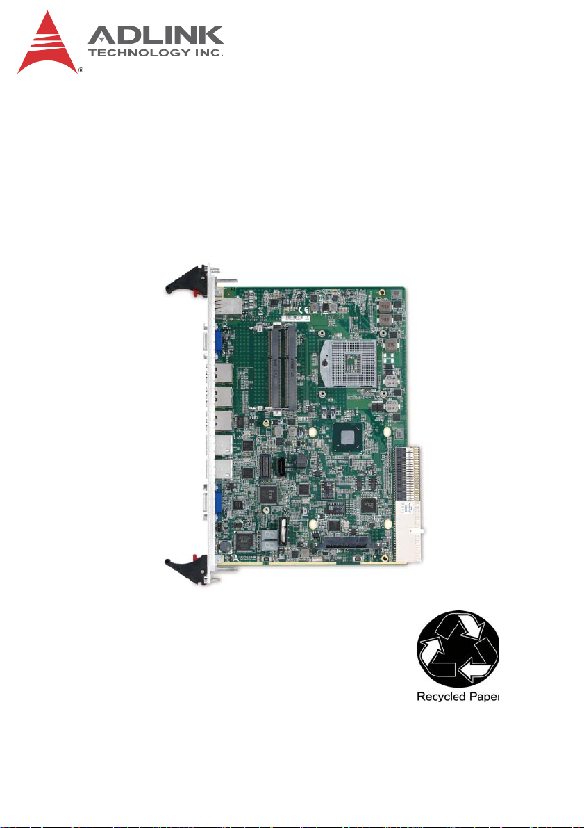
1Overview
1.1 Introduction
This manual provides information on the ADLINK cPCI-6625
Series blades. The cPCI-6625 is a 6U CompactPCI blade in dual
slot width (8HP) form factor compliant with the PICMG 2.30 CompactPCI PlusIO standard with an ultra hard metric (UHM) J2 connector. The cPCI-6626 is a 6U CompactPCI blade in dual slot
width (8HP) form factor compliant with the CompactPCI 2.0 CompactPCI R3.0 standard with hard metric J2 connector. The design
of both blades is based on the 2nd Generation Intel® Core™
i7-2710QE and Core™ i3-2330E with Mobile Intel® HM65
Express Chipset. The cPCI-6625 and the cPCI-6626 are value 6U
CompactPCI blades that offer high speed data transfer rate and
reliability.
The cPCI-6625 Series supports dual-channel un-buffered
DDR3-1066/1333 memory up to a maximum capacity of 16GB.
Graphics is integrated in the processor and output is provided
through two VGA ports on the front panel.
The cPCI-6625 Series feature four PCI-Express Intel® 82583V
Gigabit Ethernet controllers. The Ethernet connections can be
accessed through two Ethernet ports on the front panel and two
routed to J2 connector. The cPCI-6625 and cPCI-6626 also offer
six RS-232 serial ports via three RJ-45 connectors (2 serial ports
per connector), and four Type-A USB 2.0 ports on the front panel.
Storage features of the cPCI-6625 and cPCI-6626 include a SATA
6 Gb/s direct connector interface with mounting space for a 2.5"
HDD/SSD, a SATA 6Gb/s 7-pin on board and four SATA 3Gb/s
ports signals routed to J2 connector.
cPCI-6625
The cPCI-6625 Series additionally reserves one PCI-Express x4
onboard for a layer 2 expansion card that can pr ovide maxim um of
four PCI-Express x1 via Molex 74960-3018 on the front p anel. The
cPCI-6625 and the cPCI-6626 also provide four PCI-Expre ss x1 to
the J2 connector.
The cPCI-6625 Series supports the 32-bit/33MHz CompactPCI
interface and operates in a system slot only.
Overview 1
Page 14
1.2 Features
X Supports quad-core Intel® Core™ i7-2710QE or dual core
Core™ i3-2330E processor
X Up to 16GB DDR3-1333 memory in two SODIMMs
X PICMG® 2.30 CompactPCI PlusIO compliant
X PCIe x4 onboard for expansion
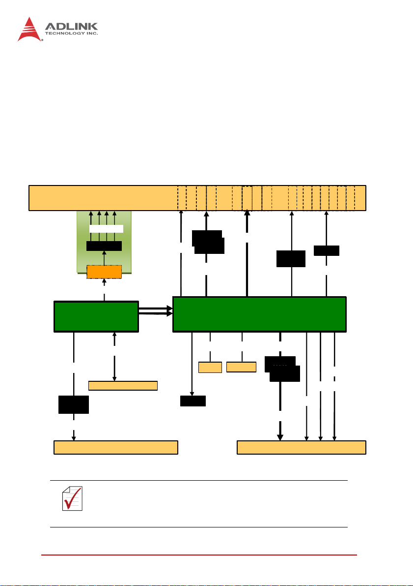
1.3 Block Diagram
Front Panel
nd
generation Core
2
i3/i7 processor
PCIe x1
PCIe to PCI
Bridge
PCI-32b/33M
VGA
GbE1
GbE2
4x PCIe x1*
PCIe Switch
B2B
PCIe x4
Intel®
DDR3-1066/1333
SODIMM, max. 8GB
DMI
FDI
RGB
SPI
BIOS
Intel
82583
Intel
82583V
2xPCIe x1
SAT A1
7-pin
J1
Figure 1-1: cPCI-6625 Series Block Diagram
USB0
USB1
USB 0/1/2/3/
HM65 PCH
Slim H DD
USB2
USB3
2x PCIe x1SAT A0
Intel
82583
Intel
82583V
2x GbE
DP to
RGB
DP
VGA
4x USB
J2
COM1
COM2
LPC
4x SATA
COM4
COM3
SIO
4x PCIe x1
COM6
COM5
Board-to-board connector reserved for 4x PCI x1 expansion to
Front Panel via daughter board. See your ADLINK representa-
NOTE:
NOTE:
tive for more information.
2Overview
Page 15

1.4 Product List
Products in the cPCI-6625 Series include:
Processor Blade
X cPCI-6625/2710/M4G: 8HP dual slot 6U cPCI PlusIO blade
featuring Intel Core i7-2710QE processor with one 4GB
DDR3 SODIMM; GbE x2, COM x6, VGA x2, USB x4,
onboard SATA 6Gb/s connector for 2.5" drive
X cPCI-6626/2330/M4G: 8HP dual slot 6U cPCI blade featur-
ing Intel Core i3-2330E processor with one 4GB DDR3
SODIMM; GbE x2, COM x6, VGA x2, USB x4, onboard
SATA 6Gb/s connector for 2.5" drive
cPCI-6625
Overview 3
Page 16

1.5 Package Contents
The cPCI-6625 is packaged with the components listed below. If
any of the items in the contents list are missing or damaged, retain
the shipping carton and packing material and contact the dealer
for inspection. Please obtain authorization before returning any
product to ADLINK. The packing contents of non-standard configurations may vary depending on customer requests.
Processor Blade
X The cPCI-6625 Series Processor Blade
Z CPU and memory specifications will differ depending on
options selected
Z Thermal module is assembled onboard
X 2.5" SATA drive accessory pack
X One RJ-45 to DB-9 COM port converter cable
X ADLINK All-in-One DVD
X User's manual
The contents of non-standard cPCI-6625 Series configurations
may vary depending on customer requests.
NOTE:
NOTE:
This product must be protected from static discharge and physical shock. Never remove any of the components except at a
CAUTION:
static-free workstation. Use the anti-static bag shipped with the
product when putting the board on a surface. Wear an
anti-static wrist strap properly grounded on one of the system's
ESD ground jacks when installing or servicing system components.
4Overview
Page 17

2 Specifications
2.1 cPCI-6625 Specifications
cPCI-6625
CompactPCI
Standard
Mechanical
Processor
Chipset Intel® HM65 Express Chipset
Memory
CompactPCI Bus
Ethernet
Graphics
Serial Ports
Storage
USB
PCI Express
PICMG® 2.0 CompactPCI® Rev. 3.0
PICMG® 2.30 CompactPCI PlusIO
Standard 6U CompactPCI®
Board size: 233.23 mm x 160 mm
Dual slot width (8HP, 40.64 mm)
CompactPCI® HM J1, UHM J2 connectors (for cPCI-6625)
CompactPCI® HM J1, J2 connectors (for cPCI-6626)
2nd Generation Intel® Core™ processor in PGA package
with passive heatsink
• Intel® Core™ i7-2710QE, 2.1GHz,6MB LLC, 45W
• Intel® Core™ i3-2330E, 2.2GHz, 3MB LLC, 35W
Dual channel unbuffered DDR3-1066/1333 memory
Two 204-pin SODIMM sockets
Up to 16GB
PCI 32-bit/33MHz; 3.3V, 5V universal V(I/O)
Supports operation in system slot only
Four PCI-Express x1 Intel® 82583V Gigabit Ethernet
controllers
Two10/100/1000 BASE-T RJ-45 LAN ports on front panel
Two routed to J2 connector
Integrated in processor with 3D engine
2x DB-15 VGA port on front panel
Supports DirectX 10.1, OpenGL 3.0
Six RS-232 serial ports from Super I/O ITE IT8783 via three
RJ-45 connectors on front panel (two RS-232 ports on each
connector by adapter cable)
One 2.5" SATA 6 Gb/s direct connector onboard
One 7-pin SATA 6 Gb/s port onboard
Four SATA 3 Gb/s ports to J2
Four USB 2.0 ports on front panel
Four USB 2.0 signals routes to J2
One PCI-Express x4 port reserved for layer 2 daughter board
Four PCI-Express x1 ports can be converted from daughter
board
Four PCI-Express ports routed to J2
Specifications 5
Page 18
Integrated in Super I/O ITE IT8783
Hardware Monitor
Monitors CPU and system temperature, DC voltages
Built-in watchdog timer
Watchdog Timer
System reset and NMI, with programmable interval, 1-65535
sec/min
BIOS AMI® EFI BIOS 64Mbit SPI flash memory
4x USB 2.0 ports (Type-A)
2x RJ-45 LAN ports
2x VGA port
Faceplate I/O
3x RS-232 COM ports in RJ-45 connectors
Storage device status LED (yellow)
Power Status LED (green)
WDT (red)
Reset button
Battery Coin cell lithium BR2032 in battery socket
Windows XP
OS Support
Windows XP embedded
Windows 7
Operating Temperature: 0°C to 70°C
Environmental
Storage Temperature: -40°C to 85°C
Operating Humidity: 95% non-condensing
Non-Operating Humidity: 95% non-condensing
Shock 15G peak-to-peak, 11ms duration, non-operating
Vibration Operating: 2Grms. 5 to 500Hz, each axis (with SSD)
Compliance CE, FCC Class A
T able 2-1: cPCI-6625 Specifications
Specifications are subject to change without prior notice.
NOTE:
NOTE:
6 Specifications
Page 19

cPCI-6625
2.2 I/O Connectivity
cPCI-6625 Processor Blade
Function Faceplate Board Rear J2
COM (RS-232) Y1 x6 — —
LAN Y x2 — Y x2
USB 2.0 Y x4 — Y x4
VGA Y x2 — —
SATA —Y
PCI Express —Y4Y x4
LEDs Y5 x3 — —
Reset Button Y——
Clear CMOS Button —Y—
Table 2-2: cPCI-6625 I/O Connectivity
Notes:
1. Six RS-232 ports via three RJ-45 connectors (two RS-232
ports on each connector by adapter cable)
2. One SATA 6 Gb/s direct connector for 2.5" onboard SATA drive
and one SATA 6 Gb/s 7-pin port onboard
3. Four SATA 3 Gb/s ports
4. One PCIe x4 ports reserved for L2 daughter board
5. Power (green), storage device (yellow), WDT (red)
2
x2 Y3 x4
Specifications 7
Page 20

2.3 Power Requirements
In order to guarantee a stable functionality of the system, it is recommended to provide more power than the system requires. An
industrial power supply unit should be able to provide at least
twice as much power as the entire system requires of each
voltage. An ATX power supply unit should be able to provide at
least three times as much power as the entire system requires.
The tolerance of the voltage lines described in the CompactPCI
specification (PICMG 2.0 R3.0) is +5%/ -3% for 5, 3.3 V and ±5%
for ±12V. This specification is for power delivered to each slot and
it includes both the power supply and the backplane tolerance.
Voltage
5V +5.0 VDC +5% / -3% 50 mV
3.3V +3.3 VDC + 5% / -3% 50 mV
+12V +12 VDC +5% / -5% 240 mV
-12V -12 VDC +5% / -5% 240 mV
V I/O (PCI I/O
Buffer Voltage)
GND
Table 2-3: CompactPCI Input Voltage Characteristics
Nominal
Value
+3.3 VDC or
+5 VDC
Tolerance
+5% / -3% 50 mV
Max. Ripple
(P - P)
8 Specifications
Page 21

cPCI-6625
Power Consumption
This section provides information on the power consumption of the
cPCI-6625 when using Intel® 2nd generation Core processors with
8GB DDR3-1333 socket memory and ADLINK ASD26-MLC32G-CT
SSD. Power consumption at 100% CPU usage was measured by
running Intel® Thermal analysis Tool 4.3..
Quad Core Intel® Core i7-2710QE, 2.1 GHz, TDP 45W
OS/Mode Current 5V Current 3.3V Total Power
DOS/Idle mode 3.65 A 1.02 A 21.62 W
Windows XP/Idle mode 2.31 A 1.00 A 14.85 W
WinXP /100%
CPU/Memory/Graphics stress
WinXP / 100%
CPU/Memory/Graphics stress
+ Windows total system stress
by BurnIn Test
Dual Core Intel® Core i3-2330E, 2.2 GHz, TDP 35W
OS/Mode Current 5V Current 3.3V Total Power
DOS/Idle mode 4.03 A 1.00 A 23.45 W
Windows XP/Idle mode 2.23 A 0.98 A 14.38 W
WinXP /100%
CPU/Memory/Graphics stress
WinXP / 100%
CPU/Memory/Graphics stress
+ Windows total system stress
by BurnIn Test
13.35 A 1.18 A 70.64 W
14.55 A 1.18 A 76.64 W
10.30 A 1.14 A 55.26 W
11.44 A 1.18 A 61.09 W
Specifications 9
Page 22

This page intentionally left blank.
10 Specifications
Page 23

3 Functional Description
The following sections describe the cPCI-6625 Series features
and functions.
3.1 Processors
The 2nd Generation Intel® Core™ processor family mobile are
64-bit, multi-core mobile processors built on 32- nanometer process
technology. Based on a new micro-architecture, the processor is
designed for a two-chip platform. The two-chip platform consists of a
processor and Platform Controller Hub (PCH). The platform enables
higher performance, lower cost, easier validation, and improved x-y
footprint. The processor includes Integrated Display Engine, Processor Graphics and Integrated Memory Controller.
The
table below lists the general specifications and power ratings
of the CPUs supported by the
Features Core™ i7-2710QE Core™ i3-2330E
No. of Cores/Threads 4/8 2/4
Clock 2.1 GHz 2.2 GHz
Max. Single Core
Turbo Freq.
Intel Smart Cache 6 MB 3 MB
DMI 5 GT/s 5 GT/s
Max. Power (TDP1)
T
junction, MAX
1. The highest expected sustainable power while running known
power intensive applications. TDP is not the maximum power
that the processor can dissipate.
2. Maximum junction temperature (T
ported operating temperature.
2
cPCI-6625 Series
3 GHz NA
45 W 35 W
100ºC 100ºC
, Max). The maximum sup-
j
.
cPCI-6625
Functional Description 11
Page 24

Supported Technologies
Features Core™ i7-2710QE Core™ i3-2330E
Intel® Turbo Boost
Technology
Intel® Hyper-Threading
Technology
Intel® vPro Technology Ye s No
Intel® Virtualization
Technology (VT-x)
Intel® Virtualization
Technology for Directed I/O
(Intel® VT-d)
Intel® Trusted Execution
Technology
Intel® 64 Architecture Yes Yes
Thermal Monitoring
Technologies
2.0 No
Yes Yes
Yes Yes
Yes No
Yes No
Yes Yes
12 Functional Description
Page 25

Interfaces
X Two channels of DDR3 memory with a maximum of one
SO-DIMM per channel
X Memory DDR3 data transfer rates of 1066 MT/s and 1333
MT/s
X 64-bit wide channels
X DDR3 I/O Voltage of 1.5 V
X 1Gb, 2Gb, and 4Gb DDR3 DRAM technologies are sup-
ported for x8 and x16 devices
X Using 4Gb device technologies, the largest memory capac-
ity possible is 16 GB, assuming dual-channel mode with two
x8, dual-ranked, un-buffered, non-ECC,
X SO-DIMM memory configuration
X The PCI Express port(s) are fully-compliant with the
PCI-Express Base Specification, Revision 2.0
X 5 GT/s point-to-point DMI interface to PCH is supported
X The Processor Graphics contains a refresh of the sixth gen-
eration graphics core enabling substantial gains in performance and lower power consumptio n.
X DX10.1, DX10, DX9 support
X OGL 3.0 support
X FDI carries display traffic from the Processor Graphics in
the processor to the legacy display connectors in the PCH
cPCI-6625
Functional Description 13
Page 26

3.2 Platform Controller Hub
The HM65 PCH provides extensive I/O support. Functions and
capabilities include:
X PCI Express Base Specification, Revision 2.0 suppor t for up
to eight ports with transfers up to 5 GT/s
X ACPI Power Management Logic Support, Revision 4.0a
X Enhanced DMA controller, interrupt controller, and timer
functions
X Integrated Serial ATA host controllers with independent
DMA operation on up to six ports
X USB host interface with two EHCI high-speed USB 2.0 Host
controllers and two rate matching hubs provide support for
up to fourteen USB 2.0 ports
X Integrated 10/100/1000 Gigabit Ethernet MAC with System
Defense
X System Management Bus (SMBus) Specification, Version
2.0 with additional support for I2C devices
X Supports Intel® High Definition Audio (Intel® HD Audio)
X Supports Intel® Rapid Storage Technology (Intel® RST)
X Supports Intel® Virtualization Technology for Directed I/O
(Intel® VT-d)
X Integrated Clock Controller
X Analog and Digital Display ports
X Low Pin Count (LPC) interface
X Firmware Hub (FWH) interface support
X Serial Peripheral Interface (SPI) support
14 Functional Description
Page 27

cPCI-6625
3.3 Intel® Turbo Boost T echnology
(Core™ i7-2710QE only)
Intel Turbo Boost Technology is a feature that allows the processor
to opportunistically and automatically run faster than its rated
operating core and/or render clock frequency when there is sufficient power headroom, and the product is within specified temperature and current limits. The Intel Turbo Boost Technology feature
is designed to increase performance of both multi-threaded and
single-threaded workloads. The processor supports a Turbo mode
where the processor can use t he th e rma l ca pacity as soc i at ed wit h
package and run at power levels higher than TDP power for
short durations. This improves the system responsiveness for
short, bursty usage conditions.
Turbo Mode availability is independent of the number of active
cores; however, the Turbo Mode frequency is d yn ami c and d epe ndent on the instantaneous application power load, the number of
active cores, user configurable settings, operating environment,
and system design. If the power, current, or thermal limit is
reached, the processor will automatically reduce the frequency to
stay with its TDP limit.
3.4 Intel® Hyper-Threading Technology
Intel® Hyper-Threading Technology allows an execution core to
function as two logical processors. While some execution
resources (such as caches, execution units, and buses) are
shared, each logical processor has its own architectural state with
its own set of general-purpose registers and control reg iste rs. This
feature must be enabled using the BIOS and requires operating
system support. Intel recommends enabling Hyper-Threading
Technology with Microsoft Windows 7, Vista, and XP, and disabling Hyper-Threading Technology using the BIOS for all pr evious versions of Windows operating systems.
Functional Description 15
Page 28

3.5 Battery
The cPCI-6625 is equipped with a 3.0V "coin cell" lithium battery
for the Real Time Clock (RTC). The lithium battery must be
replaced with an identical battery or a battery type recommended
by the manufacturer. A Rayovac BR2032 is equipped on board by
default.
16 Functional Description
Page 29

4 Board Interfaces
This chapter describes the board layout, connector pin assignments, and jumper settings of the cPCI-6625 Series.
4.1 cPCI-6625 Series Board Layout
cPCI-6625
CN6
VGA1
CN13
CN11
CN10
CN4
CN3
VGA2
LEDs
SW2
CN2
CN9
CN1
U1
U5
J2
CN8
SW1
J1
CN7
BT1
U1/U5 CPU/PCH CN1/2 SODIMM sockets
J1/J2 CompactPCI connectors CN3/4 RJ-45 LAN ports
SW1 Clear CMOS button CN6 USB 2.0 ports
SW2 Reset button CN7 SATA direct connector
LEDs HDD/Power St atus CN8 SATA 7-pin connector
BT1 Battery socket CN9 Board to board connector
VGA1/2 VGA ports CN10/11/13 RJ-45 serial ports
Figure 4-1: cPCI-6625 Series Board Layout
Board Interfaces 17
Page 30

4.2 cPCI-6625 Assembly Layout
This section illustrates the final assembly layout of the single slot
cPCI-6625 blade.
Heatsink
Figure 4-2: cPCI-6625 Assembly Layout
18 Board Interfaces
Page 31

4.3 cPCI-6625 Front Panel
1
2
3
4
USB
USB x4
USB x4 USB ports LAN RJ-45 LAN ports
COM RS-232 ports 1/2/3/4/5/6 VGA VGA connector
LEDs Power status (green)
VGA1 COM5/6 COM3/4 COM1/2 LAN BAVGA2
VGA1
COM 1/2/3/4/5/6
LAN
VGA2
Figure 4-3: cPCI-6625 Front Panel Layout
RST Reset button
HDD status (yellow)
Watch Dog Timer (WDT)
cPCI-6625
HDD
WDT
PWR
LEDs
RST
RST
Board Interfaces 19
Page 32

4.4 Connector Pin Assignments
Refer to “cPCI-6625 Series Board Layout” on page 17 and
“cPCI-6625 Front Panel Layout” on page 19 for connector locations
USB Connectors
Pin # Signal Name
1Vcc
2UV03UV0+
4GND
Table 4-1: USB Connector Pin Definition
COM Connectors
Pin # RS-232
1 DCD#, Data carrier detect
2 RTS#, Request to send
3 DSR#, Dataset ready
4 TXD, Transmit Data
5 RXD, Receive Data
6 GND, Ground
7 CTS#, Clear to send
8 DTR#, Data Terminal Ready
Table 4-2: RJ-45 Serial Port Connector Pin Definitions
20 Board Interfaces
Page 33

RJ-45 Gigabit Ethernet Connectors
cPCI-6625
Pin #
1TX+ LAN1/2_TX0+
2 TX- LAN1/2_TX03 RX+ LAN1/2_TX1+
4 -- LAN1/2_TX2+
5 -- LAN1/2_TX26 RX- LAN1/2_TX17 -- LAN1/2_TX3+
8 -- LAN1/2_TX3+
Network link is not established
or system powered off
10 Mbps
100 Mbps
1000 Mbps
10BASE-T/
100BASE-TX
Table 4-3: GbE Connector Pin Definitions
Status
Link OFF ON
Active OFF Blinking
Link Green ON
Active Green Blinking
Link Amber ON
Active Amber Blinking
1000BASE-T
Speed LED
(Green/Amber)
OFF OFF
Activity LED
81
Speed Activity
(Amber)
VGA Connector (CN6)
Signal Name Pin # Pin # Signal Name
Red 1 2 Green
Blue 3 4 N.C.
GND 5 6 GND
GND 7 8 GND
+5V. 9 10 GND
N.C. 11 12 CRTDATA
HSYNC 13 14 VSYNC
CRTCLK 15
Table 4-4: VGA Connector Pin Definition
Board Interfaces 21
Page 34

SATA Direct Connector (CN7)
Pin # Signal
S1 GND
S2 TX+
S3 TXS4 GND
S5 RXS6 RX+
S7 GND
P1 NC
P2 NC
P3 NC
P4 GND
P5 GND
P6 GND
P7 5V
P8 5V
P9 5V
P10 GND
P11 NC
P12 GND
P13~P15 NC
S1
Signal
S7
P1
Power
P15
Table 4-5: SATA Direct Connector Pin Definition
22 Board Interfaces
Page 35

cPCI-6625
CompactPCI J1 Connector Pin Assignment
Pin Z A B C D E F
25 GND +5V REQ64# ENUM# +3.3V +5V GND
24 GND AD1 +5V V(I/O) AD0 ACK64# GND
23 GND +3.3V AD4 AD3 +5V AD2 GND
22 GND AD7 GND +3.3V AD6 AD5 GND
21 GND +3.3V AD9 AD8 M66EN CBE0# GND
20 GND AD12 GND V(I/O) AD11 AD10 GND
19 GND +3.3V AD15 AD14 GND AD13 GND
18 GND SERR# GND +3.3V PAR CBE1# GND
17 GND GND IPMB_CLK IPMB_DAT GND PERR# GND
16 GND DEVSEL# GND V(I/O) STOP# LOCK# GND
15 GND +3.3V FRAME# IRDY# GND TRDY# GND
12-14 GND Key Area Key
11 GND AD18 AD17 AD16 GND CBE2# GND
10 GND AD21 GND +3.3V AD20 AD19 GND
9 GND CBE3# GND AD23 GND AD22 GND
8 GND AD26 GND V(I/O) AD25 AD24 GND
7 GND AD30 AD29 AD28 GND AD27 GND
6 GND REQ0# GND +3.3V CLK0 AD31 GND
5 GND NC NC RESET# GND GNT0# GND
4 GND +5V_IPMB HEALTHY# V(I/O) NC NC GND
3 GND IRQA# IRQB# IRQC# +5V IRQD# GND
2 GND TCK# +5V TMS# NC TDI# GND
1 GND +5V NC TRST# NC +5V GND
Table 4-6: CompactPCI J1 Connector Pin Definition
Board Interfaces 23
Page 36

CompactPCI J2 Connector Pin Assignment
Pin Z A B C D E F
22 GND GA4 GA3 GA2 GA1 GA0 GND
21 GND CLK6 GND
20 GND CLK5 GND
19 GND GND GND
18 GND
17 GND
16 GND
15 GND
14 GND
13 GND
12 GND
11 GND
10 GND
9GND
8GND
7GND
6GND
5GND
4 G ND V(I/O)
3 G ND CLK4 GND GNT3# REQ4# GNT4# GND
2 GND CLK2 CLK3 SYSEN# GNT2# REQ3# GND
1 GND CLK1 GND REQ1# GNT1# REQ2# GND
LAN3_TXDP3 LAN3_TXDP2 LAN3_TXDN0 LAN2_TXDN2 LAN2_TXDN0 GND
LAN3_TXDN3 LAN3_TXDN2 PRST# REQ6# GNT6# GND
CLK_PCIE4_N CLK_PCIE2_P DEG# GND RESERVED GND
CLK_PCIE4_P CLK_PCIE2_N FAL# REQ5# GNT5# GND
CLK_PCIE3_N CLK_PCIE1_P PCIE4_CKE SATA_CLK RESERVED GND
CLK_PCIE3_P CLK_PCIE1_N PCIE3_CKE SATA_DATAOUT SATA_LOAD GND
PCIE4_RXP PCIE1_CKE PCIE2_CKE SATA_SDI SATA_RXP5 GND
PCIE4_RXN PCIE4_TXP USB7-P SATA_TXP5 SATA_RXN5 GND
PCIE3_RXP PCIE4_TXN USB7-N SATA_TXN5 SATA_RXP4 GND
PCIE3_RXN PCIE3_TXP USB6-P SATA_TXP4 SATA_RXN4 GND
PCIE2_RXP PCIE3_TXN USB6-N SATA_TXN4 SATA_RXP3 GND
PCIE2_RXN PCIE2_TXP USB5-P SATA_TXP3 SATA_RXN3 GND
PCIE1_RXP PCIE2_TXN USB5-N SATA_TXN3 SATA_RXP2 GND
PCIE1_RXN PCIE1_TXP USB4-P SATA_TXP2 SATA_RXN2 GND
PCIE1_TXN USB4-N SATA_TXN2 RESERVED GND
LAN3_TXDP1 LAN2_TXDP3 LAN2_TXDP1 GND
LAN3_TXDN1 LAN2_TXDN3 LAN2_TXDN1 GND
LAN3_TXDP0 LAN2_TXDP2 LAN2_TXDP0 GND
Table 4-7: CompactPCI J2 Connector Pin Definition
24 Board Interfaces
Page 37

cPCI-6625
4.5 Switches
Refer to “cPCI-6625 Series Board Layout” on page 17 for switch
locations.
Reset Button (SW2)
Press Reset Button to reset the system.
Clear CMOS Switch (SW1)
Press switch SW1 to clear CMOS and reset the BIOS values to
default.
Board Interfaces 25
Page 38

This page intentionally left blank.
26 Board Interfaces
Page 39

5 Getting Started
This chapter describes the installation of the following component s
to the cPCI-6625 and rear transition modules:
X Memory modules
X 2.5" SATA storage drive
5.1 Heatsink
The cPCI-6625 Series comes with heatsink pre-installed. Removal
of the heatsink by users is not recommended. Please contact your
ADLINK service representative for assistance.
5.2 Memory Module Installation
The cPCI-6625 provides two SODIMM sockets for DDR3-1333
memory modules. Memory modules should be pre-installed on
cPCI-6625 Series blades. Follow the steps below if it is necessary
to change the memory modules
Installing a memory module
cPCI-6625
1. Insert the memory module until it properly seated shown
as below.
Getting Started 27
Page 40

2. Press down on the memory module until it is locked by
the latches on both sides..
28 Getting Started
Page 41

cPCI-6625
5.3 SATA Drive Installation
The cPCI-6625 provides space to install a slim type 2.5" SATA
storage drive. Storage drive standoffs and mounting screws are
provided in the accessory kit.
Installing a SATA Drive
1. A 2.5" SATA drive can be installed in the location indi-
cated below.
Getting Started 29
Page 42

2. Prepare a 2.5" SATA drive. Turn the SATA drive bottom
side up and secure the four standoffs provided to the
four corners of the drive.
3. Turn the drive top side up and align the drive with the
onboard SATA connector as shown. Insert the drive until
it is properly seated in the connector.
30 Getting Started
Page 43

cPCI-6625
4. Turn the cPCI-6625 solder side up, being careful to sup-
port the SA TA drive. Secure the drive with four screws as
shown below.
Support the hard drive assembly to avoid damaging the SATA
connectors when turning the board over to proceed with Step 4.
CAUTION:
Getting Started 31
Page 44

This page intentionally left blank.
32 Getting Started
Page 45

6 Drivers & Utilities
The cPCI-6625 Series drivers can be found on the ADLINK
All-In-One DVD at X:\cPCI\cPCI-6625\ or from the ADLINK website (http://www.adlinktech.com). ADLINK provides validated
drivers for Windows XP Professional and Windows 7. We recommend using these drivers to ensure compatibility.
6.1 Driver Installation Procedure
The following describes the driver installation procedures for Windows XP.
1. Install the Windows operating system before installing any
driver. Most standard I/O device drivers are installed during
Windows installation.
In order to enable AHCI mode, you must pre-install the
Intel® Rapid Storage Technology driver using the F6 instal-
NOTE:
NOTE:
2. Install the chipset driver by extracting and running the pro-
3. Install the Microsoft .NET Framework utilities (required for the
4. Install the graphics driver and utilities by extracting and run-
lation method described in the file F6Readme.txt, located
here: …\AHCI\Intel RST Driver Files_F6 Install_
32bit_11.2.0.1006.zip (not required for Windows 7).
gram in ...\Chipset\Intel_Chipset_Device_Software
_AllOS_9.2.0.1030.zip.
graphics utility) by extracting and running the program in
...\Chipset\Microsoft_Net_Framework_v3.5_SP1.zip.
ning the program in ...\Graphics\Intel_HD_Graphics
_Family_WinXP_6.14.10.5337.zip.
cPCI-6625
5. Install the LAN drivers by extracting and running the program
in …\LAN\Intel_82583V_Gigabit_Network_WINXP
_32_11.17.27.0.zip.
6. Install the Rapid Storage Technology Interface by
extracting and running the program in …\AHCI\Intel
_Rapid_Storage_Technology_32bit_10.1.0.1008.zip.
Drivers & Utilities 33
Page 46

6.2 Watchdog Timer
The sample program written in C shown below offers an interactive way to test the Watchdog Timer under DOS.
#include<stdio.h>
#include<dos.h>
static unsigned int IT8783_ioPort = 0x2e;
void Enter_IT8783_Config(unsigned int flag)
{
if(flag) IT8783_ioPort = 0x4e;
switch(IT8783_ioPort)
{
case 0x2E: //Address port = 0x2E ,
enter keys = 0x87, 0x01, 0x55, 0x55
outportb(0x2E, 0x87);
outportb(0x2E, 0x01);
outportb(0x2E, 0x55);
outportb(0x2E, 0x55);
break;
case 0x4E: //Address port = 0x4E ,
enter keys = 0x87, 0x01, 0x55, 0xAA
outportb(0x4E, 0x87);
outportb(0x4E, 0x01);
outportb(0x4E, 0x55);
outportb(0x4E, 0xAA);
break;
default:
break;
}
}
void Exit_IT8783_Config(unsigned int flag)
{
if(flag) IT8783_ioPort = 0x4e;
outportb(IT8783_ioPort, 0x02);
outportb(IT8783_ioPort+1, 0x02);
}
34 Drivers & Utilities
Page 47

cPCI-6625
void Get_IT8783_ID(unsigned int &ID1, unsigned
int &ID2)
{
outportb(IT8783_ioPort, 0x20);
ID1 = inportb(IT8783_ioPort+1);
outportb(IT8783_ioPort, 0x21);
ID2 = inportb(IT8783_ioPort+1);
}
void IT8783_1_WDTRun(unsigned int count_value,
unsigned int PLEDflag) //for
cPCI-6625
{
unsigned long tempCount;
unsigned int registerValue;
outportb(IT8783_ioPort, 0x07);
outportb(IT8783_ioPort+1, 0x07); //
Device 7
outportb(IT8783_ioPort, 0xf8);
outportb(IT8783_ioPort+1, 0x00); //
PLED mapping to nothing, disable PLED
function
if(PLEDflag == 1)
{
outportb(IT8783_ioPort, 0x28);
registerValue =
inportb(IT8783_ioPort + 1);
registerValue |= 0x04; //
set Pin76 is GPIO function GP42
outportb(IT8783_ioPort+1,
registerValue);
outportb(IT8783_ioPort, 0xc3);
registerValue =
inportb(IT8783_ioPort + 1);
registerValue &= 0xfb; //
set GP42 is alternate function
outportb(IT8783_ioPort+1,
registerValue);
Drivers & Utilities 35
Page 48

outportb(IT8783_ioPort, 0xcb);
registerValue =
inportb(IT8783_ioPort + 1);
registerValue |= 0x04; //
set GP42 is output
outportb(IT8783_ioPort+1,
registerValue);
outportb(IT8783_ioPort, 0xf8);
outportb(IT8783_ioPort+1, 0x22);
// PLED mapping to GP42
outportb(IT8783_ioPort, 0xf9);
registerValue =
inportb(IT8783_ioPort + 1);
registerValue |= 0x02;
registerValue &= 0xfb;
outportb(IT8783_ioPort+1,
registerValue);
}
outportb(IT8783_ioPort, 0x71);
registerValue = inportb(IT8783_ioPort +
1);
registerValue |= 0xD0; //
set Mouse & Keyboard interrupt Enable
outportb(IT8783_ioPort+1, registerValue);
outportb(IT8783_ioPort, 0x73);
outportb(IT8783_ioPort+1, count_value);
// set WDT count LSB
tempCount = tempCount >> 8;
outportb(IT8783_ioPort, 0x74);
outportb(IT8783_ioPort+1, count_value);
// set WDT count MSB
if(count_value >= 60)
{
outportb(IT8783_ioPort, 0x72);
registerValue =
inportb(IT8783_ioPort+1);
registerValue &= 0x8f;
36 Drivers & Utilities
Page 49

cPCI-6625
registerValue |= 0x10; //enable
WDT output through PowerOK(Pin78)
outportb(IT8783_ioPort+1,
registerValue); // set WDT count is minute
tempCount = count_value / 60;
if((count_value%60) > 30)
tempCount++;
if(tempCount > 65535)
tempCount = 65535;
printf("WDT timeout in %d
minutes.\n", tempCount);
}
else
{
outportb(IT8783_ioPort, 0x72);
registerValue =
inportb(IT8783_ioPort+1);
registerValue |= 0x80;
tempCount = count_value;
if(tempCount != 0)
{
printf("WDT timeout in %d
seconds.\n", tempCount);
registerValue |= 0x40;
//Enable WDT output through KBRST
}
else
{
printf("WDT is
Disabled.\n");
registerValue &= 0xbf;
//Disable WDT output through KBRST
}
outportb(IT8783_ioPort+1,
registerValue); // set WDT count is second
}
}
Drivers & Utilities 37
Page 50

This page intentionally left blank.
38 Drivers & Utilities
Page 51

7 BIOS Setup Utility
The following chapter describes basic navigation for the AMI EFI
BIOS setup utility.
7.1 Starting the BIOS
To enter the setup screen, follow these steps:
1. Power on the motherboard
2. Press the < Delete > key on your keyboard when you
see the following text prompt:
< Press DEL to run Setup >
3. After you press the < Delete > key, the main BIOS setup
menu displays. You can access the other setup screens
from the main BIOS setup menu.
cPCI-6625
Note: In most cases, the < Delete > key is used to invoke the setup
screen. There are several cases that use other keys, such as
< F1 >, < F2 >, and so on.
BIOS Setup Utility 39
Page 52

Setup Menu
The main BIOS setup menu is the first screen that you can navigate. Each main BIOS setup menu option is described in this
user’s guide.
The Main BIOS setup menu screen has two main frames. The left
frame displays all the options that can be configured. "Grayed"
options cannot be configured, "Blue" options can be.
The right frame displays the key legend. Above the key legend is
an area reserved for a text message. When an option is selected
in the left frame, it is highlighted in white. Often a text message will
accompany it.
40 BIOS Setup Utility
Page 53

Navigation
There is a hot key legend located in the right frame on most
setup screens.
NOTE:
NOTE:
cPCI-6625
The < F8 > key on your keyboard is the Fail-Safe key. It is not displayed on the key legend by default. To set the Fail-Safe settings
of the BIOS, press the < F8 > key on your keyboard. It is located
on the upper row of a standard 101 keyboard. The Fail-Safe settings allow the motherboard to boot up with the least amount of
options set. This can lessen the probability of conflicting settings.
Hotkey Descriptions
Enter The < Enter > key allows you to display or change the setup
option listed for a particular setup item. The < Enter > key
can also allow you to display the setup sub-screens.
F1 The < F1 > key allows you to display the General Help
BIOS Setup Utility 41
screen. Press the < F1 > key to open the General Help
screen.
Page 54

F2 The < F2 > key on your keyboard is the previous values key.
It is not displayed on the key legend by default. To set the
previous values settings of the BIOS, press the < F2 > key
on your keyboard. It is located on the upper row of a standard 101 keyboard. The previous values settings allow the
motherboard to boot up with the least amount of options set.
This can lessen the probability of conflicting settings.
F3 The < F3 > key on your keyboard is the optimized defaults
key. To set the optimized defaults settings of the BIOS, press
the < F3 > key on your keyboard. It is located on the upper
row of a standard 101 keyboard. The optimized defaults se ttings allow the motherboard to boot up with the optim ized defaults of options set. This can lessen the probability of
conflicting settings.
F4 The < F4 > key allows you to save any changes you have
made and exit Setup. Press the < F10 > key to save your
changes. The following screen will appear:
42 BIOS Setup Utility
Page 55

cPCI-6625
Press the < Enter > key to save the configuration and exit.
You can also use the < Arrow > key to select Cancel and
then press the < Enter > key to abort this function and return
to the previous screen.
ESC The < Esc > key allows you to discard any changes you have
made and exit the Setup. Press the < Esc > key to exit the
setup without saving your changes. The following screen will
appear:
Press the < Enter > key to discard changes and exit. You can
also use the < Arrow > key to select Cancel and then press
the < Enter > key to abort this function and retu rn to the previous screen.
BIOS Setup Utility 43
Page 56

7.2 Main Setup
When you first enter the Setup Utility , you will enter the Main setup
screen. You can always return to the Main setup screen by selecting the Main tab. There are two Main Setup options. They are
described in this section. The Main BIOS Setup screen is shown
below.
System Date/Time
Use this option to change the system time and date. Highlight System Time or System Date using the < Arrow > keys. En ter new values using the keyboard. Press the < Tab > key or the < Arrow >
keys to move between fields. The date must be entered in
MM/DD/YY format. The time is entered in HH:MM:SS format.
Note: The time is in 24-hour format. For example, 5:30 A.M. ap-
pears as 05:30:00, and 5:30 P.M. as 17:30:00.
44 BIOS Setup Utility
Page 57

cPCI-6625
7.3 Advanced BIOS Setup
Select the Advanced tab from the setup screen to enter the
Advanced BIOS Setup screen. You can select any of the items in
the left frame of the screen, such a s SuperIO Conf iguration, to go
to the sub menu for that item. You can display an Advanced BIOS
Setup option by highlighting it using the < Arrow > keys. The
Advanced BIOS Setup screen is shown below.
The sub menus are described on the following pages.
Launch PXE OpROM
Boot option for legacy network devices. Options: Enabled, Disabled.
Launch Storage OpROM
Boot option for legacy mass storage devices with Option ROM.
Options: Enabled/Disabled.
BIOS Setup Utility 45
Page 58

7.3.1 PCI Subsystem Settings
PCI ROM Priority
In case of multiple Option ROMs (Legacy and EFI Compatible),
specifies what PCI Option ROM to launch. Set this value to
Legacy ROM/ EFI Compatible ROM.
PCI Latency Timer
Value to be programmed into PCI Latency Timer Register.
Options: 32 PCI Bus Clocks, 64 PCI Bus Clocks, 96 PCI Bus
Clocks, 128 PCI Bus Clocks, 160 PCI Bus Clocks, 192 PCI Bus
Clocks, 224 PCI Bus Clocks, 248 PCI Bus Clocks.
VGA Palette Snoop
Enables or Disables VGA Palette Registers Snooping. Set this
value to Disable/Enable.
46 BIOS Setup Utility
Page 59

cPCI-6625
PERR# Generation
Enables or Disables PCI Device to Generate PERR#. Set this
value to Disable/Enable.
SERR# Generation
Enables or Disables PCI Device to Generate SERR#. Set this
value to Disable/Enable.
ASPM Support
Set the ASPM (Active State Power Management) level. Options:
X Disabled: Disable ASPM
X Auto: BIOS auto configure
X Force L0: Force all links to L0 State
BIOS Setup Utility 47
Page 60

7.3.2 ACPI Settings
ACPI OS Shutdown Mode
ATX: OS will turn off system power when shut down. AT: OS
shows “It is now safe to turn off your computer.” Note: AT mode
does not support S3 & S4. Set this value to ATX/ AT.
ACPI Sleep State
Select the highest ACPI sleep state the system will enter, when
the Suspend button is pressed. Options: S1(CPU Stop Clock),
Suspend Disable.
Z S1(CPU Stop Clock): Power On Suspend - Under this
setting the CPU is not executing instructions, all power
resources that supply system level reference of S0 are
off, system memory context is maintained, devices that
reference power resources that are on, and devices tha t
can wake-up the system can cause the CPU to continue
to execute from where it left off.
48 BIOS Setup Utility
Page 61

7.3.3 CPU Configuration
cPCI-6625
Hyper-Threading
Enables/disables Hyper-Threading Technology. Enable for
Windows XP and Linux (OS optimized for Hyper-Threading
Technology) and disable for other OS (OS not optimized for
Hyper-Threading Technology.
Active Processor Cores
Number of cores to enable in each processor package.
Options: All, 1.
Limit CPUID Maximum
When the computer is boots, the operating system executes its
CPUID instruction to identify the processor and its capabilities.
Before it can do so, it must first query the processor to find out
the highest input value the CPUID recognizes. This determines
the kind of basic information CPUID can provide the operating
system. This option allows you to circumvent problems with
BIOS Setup Utility 49
Page 62

older operating systems. When Enabled, the processor will
limit the maximum CPUID input value to 03h when queried,
even if the processor supports a higher CPUID input value.
When Disabled, the processor will return the actual maximum
CPUID input value of the processor when queried.
Execute Disable Bit
XD can prevent certain classes of malicious buffer overflow
attacks when combined with a supporting OS.(Windows Server
2003 SP1, Windows XP SP2, SuSE Linux 9.2 Red Hat Enterprise 3 Update 3.)
Intel Virtualization
Enables/disables Intel Virtualization Technology.
50 BIOS Setup Utility
Page 63

7.3.4 SATA Configuration
cPCI-6625
SATA Controlle r(s)
This item enables/disables the SATA Controllers.
SATA Mode Selection
The SATA interface can be configured as legacy IDE or AHCI
mode.
SATA Port 0~5
Display SATA device name string.
Staggered Spin-up
Appears when SATA mode is set to AHCI. AHCI Support Staggered Spin-up. Set this value to Enable/Disable.
BIOS Setup Utility 51
Page 64

External SATA Port
Appears when SATA mode is set to AHCI. eSATA Ports Support. Set this value to Enable/Disable.
Hot Plug
Appears when SATA mode is set to AHCI. SATA Ports Hot Plug
support. Set this value to Enable/Disable.
52 BIOS Setup Utility
Page 65

7.3.5 USB Configuration
cPCI-6625
Legacy USB Support
Enables legacy USB support. Auto option disables legacy support if no USB devices are connected. Disable option will keep
USB devices available only for EFI applications. Set this value
to Enable/Disable/Auto.
EHCI Hand-off
This is a workaround for OSes without EHCI hand-off support.
The EHCI ownership change should be claimed by the EHCI
driver. Op tions: Enable, Disable.
BIOS Setup Utility 53
Page 66

7.3.6 Super IO Configuration
Serial Port 1~6 Configuration
Each sub-menu allows you to enable/disable Serial Ports 1~6.
Serial port address and IRQ are not configurable.
NOTE:
NOTE:
54 BIOS Setup Utility
Page 67

7.3.7 Hardware Monitor
cPCI-6625
BIOS Setup Utility 55
Page 68

7.3.8 Serial Port Console Redirection
The settings specify how the host computer and the remote
computer will exchange data. Both computers should have the
same or compatible settings.
Console Redirection
Enable or disable Console Redirection.
Console Redirection Settings
The settings specify how the host computer and the remote
computer (which the user is using) will exchange data. Both
computers should have the same or compatible settings. The
screen is shown below.
56 BIOS Setup Utility
Page 69

cPCI-6625
Terminal Type
VT-UTF8 is the preferred terminal type for out-of-band management. The next best choice is VT100+ and then VT100.
Options: VT100, VT100+, VT-UTF8, ASNI.
Bits per Second
Select the bit rate (bits/second) you want the serial port to use
for console redirection. Options: 115200, 57600, 19200, 9600.
Data Bits
Select the data bits you want the serial port to use for console
redirection. Set this value to 7 or 8.
Parity
Set this option to select Parity for console redirection. The settings for this value are None, Even, Odd, Mark, Space.
BIOS Setup Utility 57
Page 70

Stop B its
Stop bits indicate the end of a serial data packet. (A start bit
indicates the beginning). The standard setting is 1 stop bit.
Communication with slow devices may require more than 1
stop bit. Set this value to 1 or 2.
Flow Control
Set this option to select Flow Control for console redirection.
The settings for this value are Noneand Hardware RTS/CTS.
Flow control can prevent da ta loss from buffer overflow. When
sending data, if the receiving buffers are full, a 'stop' signal can
be sent to stop the data flow. Once the buffers are empty, a
'start' signal can be sent to re-star t the flow. Hardware flow control uses two wires to send start/stop signals. Software flow
control uses start/stop ASCII chars, which slows down the data
flow and can be problematic if binary data is being sent.
Recorder Mode
When enabled, only text will be sent. This is to capture terminal
data.
Resolution 100x31
Enables or disables extended terminal resolution.
Legacy OS Redirection Resolution
In legacy OSes, the number of rows and columns supported by
redirection. The settings for this value are: 80x24, 80x25.
58 BIOS Setup Utility
Page 71

7.3.9 CPU PPM Configuration
(Processor Power Management)
cPCI-6625
EIST
Enables/disables Enhanced Intel SpeedStep® Technology
(EIST)
CPU C3 Report
Enable or disable CPU C3 (ACPI C2) report to OS. Set this
value to Enable/Disable.
CPU C6 Report
Enable or disable CPU C6 (ACPI C3) report to OS. Set this
value to Enable/Disable.
CPU C7 Report
Enable or disable CPU C7 (ACPI C3) report to OS. Set this
value to Enable/Disable.
BIOS Setup Utility 59
Page 72

7.4 Chipset Configuration
Select the Chipset tab from the setup screen to enter the Chipset
BIOS Setup screen. You can select any of Chipset BIOS Setup
options by highlighting it using the < Arrow > keys. The Chipset
BIOS Setup screen is shown below.
60 BIOS Setup Utility
Page 73

7.4.1 System Agent (SA) Configuratio
cPCI-6625
VT-d
Intel Virtualization Technology for Directed I/O. Set this value to
Enable/Disable.
BIOS Setup Utility 61
Page 74

Graphics Configuration
Graphics Turbo IMON Current
Set the value which graphics Turbo IMON supported (14~31).
Primary Display
Allows you to select which graphics controller to use as the primary boot device. Options: Auto, IGFX, PEG, PCI.
Internal Graphics
Allows you to select enable/disable.the internal graphics.
Options: Auto, Enabled or Disabled
GTT Size
Select the GTT Size. Set this value to 1MB / 2MB.
Aperture Size
Select the Aperture Size. Set this value to 128MB / 256MB /
512MB.
DVMT Pre-Allocated
Select DVMT 5.0 Pre-Allocated (fixed) graphics memory size
used by the internal graphics device. Configuration options is
as below screen:
62 BIOS Setup Utility
Page 75

cPCI-6625
DVMT Total Gfx Memory
Select DVMT 5.0 total graphic memory size used by the internal graphics
device. Configuration options is as below screen :
Gfx Low Power Mode
This option is applicable for SFF only. Set this value to
Enable/Disable.
BIOS Setup Utility 63
Page 76

Memory Information
Memory Remap
Enable or disable memory remap above 4G. Set this value to
Enable/Disable.
64 BIOS Setup Utility
Page 77

7.4.2 PCH-IO Configuration
cPCI-6625
Onboard 82583 LAN Controller
Enable or disable onboard 82583 Lan 1/2/3/4 Controller. Set
this value to Enable/Disable
High Precision Timer
Enable or Disable the High Precision Event Timer. Set this
value to Enable/Disable.
BIOS Setup Utility 65
Page 78

USB Configuration
EHCI1 Controller 1
USB 2.0 (EHCI) support. Set this value to Enable/Disable.
USB Ports Per-Port Disable Control
Control each of the USB ports (0~13) disabling. Set this value
to Enable / Disable.
66 BIOS Setup Utility
Page 79

cPCI-6625
PCI Express Configuration
PCI Express Clock Gating
Enable or disable PCI Express Clock Gating for each root port.
Set this value to Enable / Disable.
DMI Link ASPM Control
The control of Active State Power Management on both NB
side and SB side of the DMI Link. Set this value to Disable/L0s/L0sL1.
DMI Link Extended Synch Control
The control of Extended Synch on SB side of the DMI Link.
Subtractive Decode
Enable or disable PCI Express Subtractive Decode. Set this
value to Enable / Disable.
PCI Express Root Port 5~8
Control the PCI Express Root Port of 5~8
BIOS Setup Utility 67
Page 80

7.5 Boot Configuration
Select the Boot tab from the setup screen to enter the Boot Configuration screen. You can select any of the items in the left frame
of the screen to go to the sub menu for that item. You can display
a Boot Configuration option by highlighting it using the < Arrow >
keys. The Boot Configuration screen is shown below:
Quiet Boot
When this feature is enabled, the BIOS will hide normal POST
messages during the boot-u p sequence. When it is disabled, the
BIOS will display the normal POST messages.
Fast Boot
Enables or disables boot with initialization of a minimal set of
devices required to launch active boot option. Has no effect for
BBS boot options. Set this value to Enable / Disable.
68 BIOS Setup Utility
Page 81

cPCI-6625
Set Boot Priority
Set Boot Option #1 ~2 boot priority.
Hard Disk Drive BBS Priorities
Specifies the boot device priority sequence from available hard
drives.
7.6 Security Setup
Administrator Password
Use this option to set a password for administrators with full control of the BIOS setup utility.
User Password
Use this option to set a password for users with limited access to
the BIOS setup utility .
BIOS Setup Utility 69
Page 82

7.7 Save & Exit
Select the Save & Exit tab from the setup screen to enter the Save
& Exit setup screen. You can display a Save & Exit BIOS setup
option by highlighting it using the < Arrow > keys. The Save & Exit
BIOS setup screen is shown below.
Save Changes and Exit
When you have completed the system configuration changes,
select this option to leave Setup and reboot the computer so the
new system configuration parameters can take effect.
Discard Changes and Exit
Select this option to quit Setup without making any permanent
changes to the system configuration.
70 BIOS Setup Utility
Page 83

Save Changes and Reset
Reset the system after saving the changes.
Discard Changes and Reset
Reset the system without saving any changes.
Save Changes
Save changes made so far to any of the setup options.
Discard Changes
Discard changes made so far to any of the setup options.
Restore Defaults
Restore/Load Defaults values for all the setup options.
Save as User Defaults
Save changes made so far as User Defaults.
Restore User Defaults
cPCI-6625
Restore the User Defaults to all setup options
Boot Override
Use the up/down arrow keys to highlight a boot device to immediately exit the BIOS Setup and boot from the selected device.
Launch EFI Shell from file system device
Attempts to Launch EFI Shell application (Shellx64.e fi) from one of
the available file system devices.
BIOS Setup Utility 71
Page 84

This page intentionally left blank.
72 BIOS Setup Utility
Page 85

cPCI-6625
Important Safety Instructions
For user safety, please read and follow all instructions,
WARNINGS, CAUTIONS, and NOTES marked in this manual
and on the associated equipment before handling/operating the
equipment.
X Read these safety instructions carefully.
X Keep this user’s manual for future reference.
X Read the specifications section of this manual for detailed
information on the operating environment of this equipment.
X When installing/mounting or uninstalling/removing
equipment:
Z Turn off power and u nplug any power cords/cables.
X To avoid electrical shock and/or damage to equipment:
Z Keep equipment away from water or liquid sources;
Z Keep equipment away from high heat or high humidity;
Z Keep equipment properly ventilated (do not block or
cover ventilation openings);
Z Make sure to use recommended voltage and powe r
source settings;
Z Always install and operate equipment near an easily
accessible electrical socket-outlet;
Z Secure the power cord (do not place any obje ct on /ove r
the power cord);
Z Only install/attach and operate equipment on stable
surfaces and/or recommended mountings; and,
Z If the equipment will not be used for long periods of time,
turn off and unplug the equipment from its power source.
Important Safety Instructions 73
Page 86

X Never attempt to fix the equipment. Equipmen t sho u ld on ly
be serviced by qualified personnel.
A Lithium-type battery may be provided for uninterrupted, backup
or emergency power.
Risk of explosion if battery is replaced with one of an incorrect
WARNING:
type. Dispose of used batteries appropriately.
X Equipment must be serviced by authorized technicians
when:
Z The power cord or plug is damaged;
Z Liquid has penetrated the equipment;
Z It has been exposed to high humidity/moisture;
Z It is not functioning or does not function according to the
user’s manual;
Z It has been dropped and/or damaged; and/or,
Z It has an obvious sign of breakage.
74 Important Safety Instructions
Page 87

Getting Service
Contact us should you require any service or assistance.
ADLINK Technology, Inc.
Address: 9F, No.166 Jian Yi Road, Zhonghe District
New Taipei City 235, Taiwan
ᄅקؑխࡉ৬ԫሁ 166 ᇆ 9 ᑔ
Tel: +886-2-8226-5877
Fax: +886-2-8226-5717
Email: service@adlinktech.com
Ampro ADLINK Technology, Inc.
Address: 5215 Hellyer Avenue, #110
San Jose, CA 95138, USA
Tel: +1-408-360-0200
Toll Free: +1-800-966-5200 (USA only)
Fax: +1-408-360-0222
Email: info@adlinktech.com
ADLINK Technology (China) Co., Ltd.
Address: Ϟ⍋Ꮦ⌺ϰᮄᓴ∳催⾥ᡔು㢇䏃 300 ো(201203)
300 Fang Chun Rd., Zhangjiang Hi-Tech Park
Pudong New Area, Shanghai, 201203 China
Tel: +86-21-5132-8988
Fax: +86-21-5132-3588
Email: market@adlinktech.com
cPCI-6625
ADLINK Technology Beijing
Address: ࣫ҀᏖ⍋⎔Ϟഄϰ䏃 1 োⲜ߯ࡼ E ᑻ 801 ᅸ(100085)
Beijing, 100085 China
Tel: +86-10-5885-8666
Fax: +86-10-5885-8626
Email: market@adlinktech.com
ADLINK Technology Shenzhen
Address: ⏅ഇᏖቅ⾥ᡔು催ᮄϗ䘧᭄ᄫᡔᴃು
Tel: +86-755-2643-4858
Fax: +86-755-2664-6353
Email: market@adlinktech.com
LiPPERT ADLINK Technology GmbH
Address: Hans-Thoma-Strasse 11, D-68163
Mannheim, Germany
Tel: +49-621-43214-0
Fax: +49-621 43214-30
Email: emea@adlinktech.com
Rm. 801, Power Creative E, No. 1 Shang Di East Rd.
A1 2 ὐ C (518057)
2F, C Block, Bldg. A1, Cyber-Tech Zone, Gao Xin Ave. Sec. 7
High-Tech Industrial Park S., Shenzhen, 518054 China
Getting Service 75
Page 88

ADLINK Technology, Inc. (French Liaison Office)
Address: 6 allée de Londres, Immeuble Ceylan
91940 Les Ulis, France
Tel: +33 (0) 1 60 12 35 66
Fax: +33 (0) 1 60 12 35 66
Email: france@adlinktech.com
ADLINK Technology Japan Corporation
Address: ͱ101-0045 ᵅҀ䛑ҷ⬄⼲⬄䤯ފ⬎ 3-7-4
Tel: +81-3-4455-3722
Fax: +81-3-5209-6013
Email: japan@adlinktech.com
ADLINK Technology, Inc. (Korean Liaison Office)
Address: 137-881 昢殾柢 昢爎割 昢爎堆嵢 326, 802 (昢爎壟, 微汾瘶捒娯)
Tel: +82-2-2057-0565
Fax: +82-2-2057-0563
Email: korea@adlinktech.com
ADLINK Technology Singapore Pte. Ltd.
Address: 84 Genting Lane #07-02A, Cityneon Design Centre
Tel: +65-6844-2261
Fax: +65-6844-2263
Email: singapore@adlinktech.com
ADLINK Technology Singapore Pte. Ltd. (Indian Liaison Office)
Address: #50-56, First Floor, Spearhead Towers
Malleswaram, Bangalore - 560 055, India
Tel: +91-80-65605817, +91-80-42246107
Fax: +91-80-23464606
Email: india@adlinktech.com
⼲⬄ 374 ɛɳ 4F
KANDA374 Bldg. 4F, 3-7-4 Kanda Kajicho,
Chiyoda-ku, Tokyo 101-0045, Japan
802, Mointer B/D, 326 Seocho-daero, Seocho-Gu,
Seoul 137-881, Korea
Singapore 349584
Margosa Main Road (between 16th/17th Cross)
ADLINK Technology, Inc. (Israeli Liaison Office)
Address: 27 Maskit St., Corex Building
PO Box 12777
Herzliya 4673300, Israel
Tel: +972-77-208-0230
Fax: +972-77-208-0230
Email: israel@adlinktech.com
ADLINK Technology, Inc. (UK Liaison Office)
Tel: +44 774 010 59 65
Email: UK@adlinktech.com
76 Getting Service
 Loading...