

Page 1
cPCI-6525
6U CompactPCI® 3rd Generation
Intel® Core™ i7 Processor Blade
User’s Manual
Manual Rev.: 0.10 preliminary
Revision Date: April 17, 2015
Part No: 50-15101-1010
Advance Technologies; Automate the World.
Page 2

Revision History
Revision Release Date Description of Change(s)
0.10 2015/04/17 Preliminary release
Page 3

cPCI-6525
Preface
Copyright 2015 ADLINK Technology Inc.
This document contains proprietary infor mation protected by copyright. All rights are reserved. No part of this manual may be reproduced by any mechanical, electronic, or other means in any form
without prior written permission of the manufacturer.
Disclaimer
The information in this document is subject to change without prior
notice in order to improve reliability, design, and function and does
not represent a commitment on the part of the manufa cturer.
In no event will the manufacturer be liable for direct, indirect, special, incidental, or consequential damages arising out of the use or
inability to use the product or documentation, even if advised of
the possibility of such damages.
Environmental Responsibility
ADLINK is committed to fulfill its social responsibility to global
environmental preservation through compliance with the European Union's Restriction of Hazardous Substances (RoHS) directive and Waste Electrical and Electronic Equipment (WEEE)
directive. Environmental protection is a top priority for ADLINK.
We have enforced measures to ensure that our products, manufacturing processes, components, and raw materials have as little
impact on the environment as possible. When products are at their
end of life, our customers are encouraged to dispose of them in
accordance with the product disposal and/or recovery programs
prescribed by their nation or company.
Trademarks
Product names mentioned herein are used for identification purposes only and may be trademarks and/or registered trademarks
of their respective companies.
Preface iii
Page 4
Conventions
Take note of the following conventions used throughout this
manual to make sure that users perform certain tasks and
instructions properly.
Additional information, aids, and tips that help users perform
tasks.
NOTE:
NOTE:
Information to prevent minor physical injury, component damage, data loss, and/or program corruption when trying to com-
CAUTION:
WARNING:
plete a task.
Information to prevent serious physical injury, component
damage, data loss, and/or program corruption when trying to
complete a specific task.
iv Preface
Page 5

cPCI-6525
Table of Contents
Revision History...................................................................... ii
Preface.................................................................................... iii
List of Figures....................................................................... vii
List of Tables.......................................................................... ix
1 Introduction ........................................................................ 1
1.1 Overview.............................................................................. 1
1.2 Features............................................................................... 3
1.3 Block Diagram ..................................................................... 4
1.4 Product List............................. ... .......................................... 5
1.5 Package Contents ............................................................... 6
2 Specifications..................................................................... 7
2.1 cPCI-6525 Blade Specifications .......................................... 7
2.2 I/O Connectivity ................................................................... 9
2.3 Power Requirements.................... ... .... ... ... ... ... .... ... ... ... .... . 10
3 Functional Description .................................................... 13
3.1 Processors......................................................................... 13
3.2 Chipset............................................................................... 15
3.3 Intel® Turbo Boost Technology......................................... 16
3.4 Intel® Hyper Threading Technology.................................. 16
3.5 Intel® Active Management Technology............................. 16
3.6 TPM................................................................................... 17
3.7 Battery ............................................................................... 17
4 Board Interfaces............................................................... 19
4.1 Board Layout - Front.......................................................... 19
4.2 Board Layout - Back.......................................................... 20
Table of Contents v
Page 6

4.3 cPCI-6525 Front Panel ...................................................... 21
4.4 Connector Pin Assignments............................................... 22
4.5 Buttons, Switches and Jumpers................................... ... ... 33
5 Checkpoints & Beep Codes............................................. 37
5.1 Checkpoint Ranges............................... .... ... ... ... ... .... ... ... ... 37
5.2 Standard Checkpoints........................................................ 37
5.3 OEM-Reserved Checkpoint Ranges.................................. 46
Important Safety Instructions............................................... 47
Getting Service...................................................................... 49
vi Table of Contents
Page 7

cPCI-6525
List of Figures
Figure 1-1: cPCI-6525 Functional Block Diagram..............................4
Figure 4-1: cPCI-6525 Board Layout - Front................. .... ...............19
Figure 4-2: cPCI-6525 Board Layout - Back ..... ... ... ... ... .... ... ............20
Figure 4-3: cPCI-6525 Front Panel .................................................. 21
List of Figures vii
Page 8

This page intentionally left blank.
viii List of Figures
Page 9

cPCI-6525
List of Tables
Table 2-1: cPCI-6525 Blade Specifications ...................................... 7
Table 2-2: cPCI-6525 I/O Connectivity .............................................9
Table 4-1: DVI-I Connector Pin Definition....................................... 24
List of Tables ix
Page 10

This page intentionally left blank.
xList of Tables
Page 11

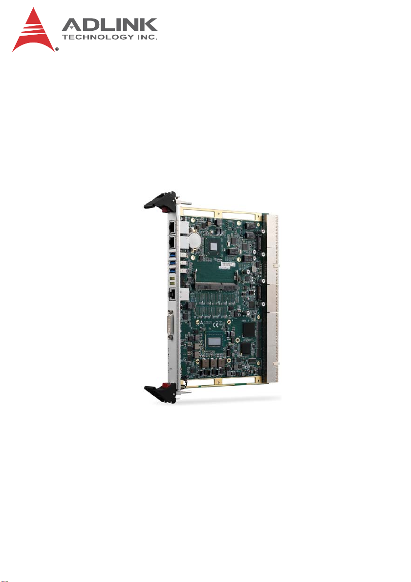
1 Introduction
1.1 Overview
The cPCI-6525 is a 6U CompactPCI® processor blade in single-slot (4HP) width form factor featuring a single 22nm FC-BGA
3rd generation Intel® Core™ i7 Processor with quad-cores mated
with the Mobile Intel® QM77 Express Chipset. The cPCI-6525
supports dual channel DDR3-1333/1600 ECC SDRAM with one
channel in a SO-CDIMM socket and one channel of soldered
onboard memory (total memory capacity up to 16GB). Graphics is
integrated in the Intel processor with one DVI-I port on the front
panel switchable to rear IO. The cPCI-6525 has two GbE cont rollers (Intel® 82574IT) providing two GbE ports on the front panel
(switchable to rear) and two Intel® 82574IT GbE controllers providing two ports to rear IO. For expansion flexibility, the cPCI-6525
routes one PCIe x16 Gen2 (convertible to two PCIe x8 Gen2) and
one PCIe x4 to rear IO.
Additional IO functionality of the cPCI-6525 includes three USB
3.0 ports and one RS-232/422/485 serial port via RJ-45 connector
on the front panel. Onboard storage capabilities include a SATA 6
Gb/s direct connector for a 2.5" drive and CFast slot via adapter
board. The cPCI-6525 is also equipped with an Atmel
AT97SC3204 Trusted Platform Module (TPM) to meet security
requirements.
Rear I/O functionality includes two GbE ports via two Intel®
82574IT GbE controllers for PICMG 2.16 support, two GbE ports
(switchable from front panel), six USB 2.0, PS/2 keyboard/mouse,
three serial ports, two DVI interfaces, and HD Audio. Available
rear I/O for storage includes three SATA ports (dependent on
selected RTM) and eight SAS ports supporting hardware RAID via
two mini-SAS x4 connectors when mated with the cPCI-R66S0
RTM. By selecting cPCI-R66G0 or cPCI-R66N0 RTM, the
cPCI-6525 can utilize an MXM PCIe x16 graphics card to perform
high speed calculations.
cPCI-6525
Introduction 1
Page 12

The cPCI-6525 supports operation in both a system slot and in a
peripheral slot as a standalone blade. The cPCI-6525 is compliant
with the PICMG 2.9 specification and supports system management functions based on the Intelligent Platform Management
Interface (IPMI) as well as hardware monitoring of physical characteristics such as CPU and system temperature, DC voltages
and power status.
The cPCI-6525 is ideal for demanding applications, providing system integrators in military, communications and other critical applications a best-performance-per-watt, high I/O throughput solution
with a reliable, smooth path for scalability and expansion.
2Introduction
Page 13

1.2 Features
X 6U CompactPCI® processor blade in 4HP width form factor
X Quad-core 3rd Generation Intel® Core ™ i7- 361 5QE
2.3GHz, 6MB L3 Cache, 45W TDP, FCBGA pa ckage
X Mobile Intel® QM77 Express Chipset (Intel® BD82QM77
PCH)
X Dual channel DDR3-1066/1333 ECC SDRAM up to 16GB,
one channel soldered up to 8GB, one channel SO-CDIMM
up to 8GB
X 32/64-bit, 33/66MHz CompactPCI® Interface based on PCI
specifications, universal V(I/O)
X Supports Satellite Mode operation as a standalone blade in
peripheral slots
X Three USB 3.0 ports from PCH
X SATA 6 Gb/s direct connector for onboard 2.5" drive
X CFast slot via adapter board
X 8x general purpose user programmable LEDs on front
panel (default: Port 80 status)
X One DVI-I on front panel with RGB signal switcha ble to rear
and two additional DVI routed to rear
X Two GbE ports on front panel via Intel® 82574IT and
82579LM, switchable to rear
X Two Gigabit Ether net ports to rear via Intel® 82574IT con-
trollers
X Compliant with PICMG 2.0, 2.1, 2.9, 2.16 standards
X Atmel AT97SC3204 TPM support (optional)
X Eight SAS/SATA ports supported by LSISAS3008 when
mated with cPCI-R66S0 RTM
X MXM PCIe x16 graphics when mated with cPCI-R66G0 and
cPCI-R66N0
cPCI-6525
Introduction 3
Page 14
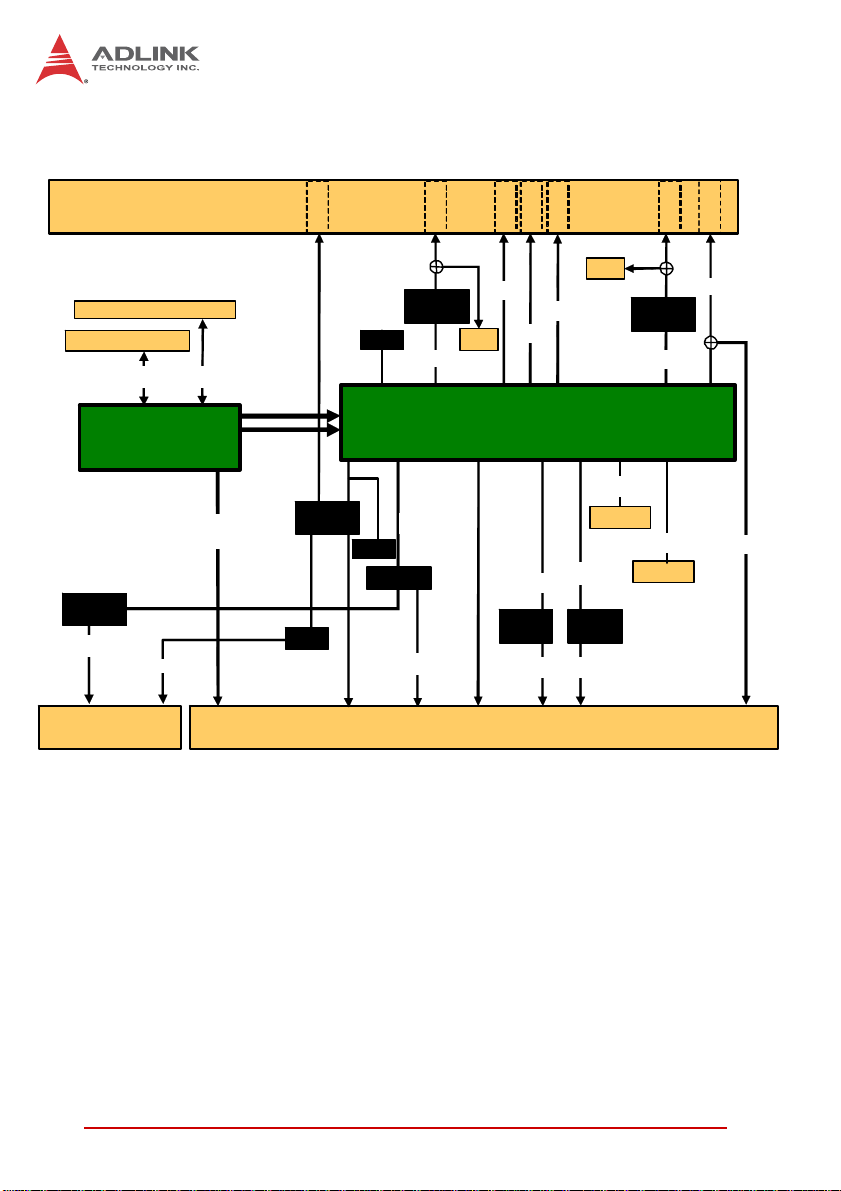
1.3 Block Diagram
Front Panel
COM1
GbE1
USB1
USB2
USB 3
GbE2
DVI-I
COM1
BIOS
PCIe Switch
PCIe x4
82574I T
PCIe x1
PCI e x4
Intel
ECC SO-CDIMM, max. 8GB
Sol dered ECC, max. 8GB
DDR3 1333/1600
rd
Gen Intel® Core i7
3
PI7C9 X130
PCI 64b/66M
IPMB 0 /1
PCIe x16
or 2x PCIe x8
DMI
FDI
COM6
BMC
SIO
LPC
SPI
TPM
KB/M S
COM2/3/5
J1/J2 J3/J4/J5
Figure 1-1: cPCI-6525 Functional Block Diagram
USB 3.0
USB 3.0
USB 3.0
J5
Intel®QM77 PCH
6x USB 2.0
3x SAT A
HDA
RTC
DVI 2/3
GPIO
PCIe x1
Inte l
82574IT
GbE3 GbE 4
PCIe x1
8257 4IT
J5
SATA0
2.5” HDD
Intel
Intel
82574 IT
PCIe x1
SATA4
B2B
DVI
RGB
4Introduction
Page 15

1.4 Product List
Processor Blade
X cPCI-6525: 4HP width (single-slot) 6U CompactPCI Pro-
cessor Blade
Rear Transition Module
X cPCI-R66S0: 6U 8HP width RTM with DVI-D, 1x COM, 3x
USB, 4x GbE, 4x eSAS/SATA, 4x iSAS/SATA, PS/2 KB/MS
and Line-in/out
X cPCI-R66N0: 6U 8HP width RTM with DVI-I, DVI-D, 1x
COM, and 1x USB, 2x GbE (RJ-45); onboard MXM slot; 2x
GbE, audio, KB/MS via M12 connector
X cPCI-R66G0: 6U 8HP width RTM with 3x DVI-D, 1x DVI-I,
1x USB, 1x PS/2 KB/MS, audio, onboard MXM slot
cPCI-6525
Introduction 5
Page 16
1.5 Package Contents
The cPCI-6525 is packaged with the following components. If any
of the items on the contents list are missing or damaged, retain the
shipping carton and packing material and contact the dealer for
inspection. Please obtain authorization before returning any product to ADLINK. The packing contents of the cPCI-6525 are
non-standard configurations and may vary depending on customer
requests.
Processor Blade
X cPCI-6525
Z CPU and memory specifications will differ depending on
options selected
Z Thermal module is assembled on the board
X RJ-45 to DB-9 cable for RJ-45 COM port
X 2.5" SATA drive mounting kit, including bracket and screws
for 2.5" SATA drive and DB-LSATA adapter card
X CFast socket kit, including DB-CFAST adapter board and
mounting hardware
X ADLINK All-in-One DVD
X User’s manual
The contents of non-standard cPCI-6525 configurations may
vary depending on the customer requirements.
NOTE:
NOTE:
This product must be protected from static discharge and physical shock. Never remove any of the components except at a
CAUTION:
static-free workstation. Use the anti-static bag shipped with the
product when putting the board on a surface. Wear an
anti-static wrist strap properly grounded on one of the system's
ESD ground jacks when installing or servicing system components.
6Introduction
Page 17

2 Specifications
2.1 cPCI-6525 Blade Specifications
cPCI-6525
CompactPCI®
Standards
Mechanical • Standard 6U CompactPCI®
Processor 22nm FCBGA Intel® Core™ i7 Processor
Chipset • Intel® BD82QM77 Platform Controller Hub (PCH)
Memory • Dual channel DDR3-1066/1333/1600 SDRAM with ECC,
CompactPCI
Bus
Graphics • Integrated in processor
BIOS • AMI EFI BIOS, 64Mbit SPI flash memory
Gigabit
Ethernet
• PICMG® 2.0 CompactPCI® Rev. 3.0
• PICMG® 2.1 Hot Swap Specification Rev.2.0
• PICMG® 2.9 System Management Bus Rev. 1.0
• PCIMG® 2.16 Packet Switching Backplane Rev.1.0
• Board size: 233.35mm x 160mm
• Single-slot width (4HP, 20.32mm)
• CompactPCI® connectors with J1, J2, J3, J4 and J5
• UHM connector at J4 for PCIe x16 high speed transmission
(optional)
• 4-core Intel® Core i7-3615QE Processor, 2.3 GHz, 6MB L3
cache, TDP 45W
• 4-core Intel® Core i7-3612QE Processor, 2.1 GHz, 6MB L3
cache, TDP 35W
• Passive heatsink
total up to 16GB
• One channel in SODIMM sockets up to 8GB
• One channel soldered onboard up to 8GB (dependent on
availability of memory modules and chips)
• PCI 32/64-bit, 33/66MHz; 3.3V, 5V universal V(I/O)
• Supports operation in system slot as master or in peripheral
slot as standalone blade without connectivity to
CompactPCI bus (Satellite mode)
• Two dual mode DisplayPorts on front panel with
DVI/VGA/HDMI support by adapter cable
• One DVI, eDP and VGA routed to rear
• Two front panel GbE ports from Intel® 82579LM and
82574IT, switchable to rear
• Two rear IO GbE 10/100/1000BASE-T ports by Intel
82574IT GbE controller (PICMG 2.16 support)
Table 2-1: cPCI-6525 Blade S pecifications
Specifications 7
Page 18
Serial Ports Four16C550 serial ports
• One DB-9 RS-232/422/485 serial port on front panel
• Three serial ports routed to rear I/O through J3 (1x RS232/422/485, 2x TX/RX only)
PCI Express • PCI e x1 6 Ge n 2 to J4
• PCIe x4 Gen2 to J5
USB 2.0 • Six USB 2.0 ports routed to J3
USB 3.0 • Three USB 3.0 ports on front panel, one to J5
KB/MS • PS/2 Keyboard/Mouse port to J3
Audio • High Definition Audio signals routed to J3
TPM Atmel AT97SC3204 TPM (upon request)
• Over/Under voltage detection
• Low/High frequency sensor/filter
• Reset filter
• Memory Encryption/Decryption
Storage
Interfaces
• One SATA 6 Gb/s direct connector for 2.5" onboard drive
1
(removable)
1
• One SATA 6 Gb/s CFast slot by adapter board
• Thre e SATA 3Gb/s to rear IO
Faceplate I/O • 2x 10/100/1000BASE-T Ethernet ports
• 1x DVI-I (RGB switchable to rear)
• 3x USB 3.0 ports
• 1x RJ-45 RS-232/422/485 port
OS
Compatibility
• Microsoft Windows 7 32/64-bit
• Red Hat Enterprise Linux 6.2 x86 64-bit
• Fedora 16 x86 64-bit
• Wind River VxWorks 6.9 BSP
• Other OS supp ort on request
Environmental • Operating Temperature2:
Standard: 0 to 60°C with forced air flow
ETT: -20°C to 70°C with forced air flow (cPCI-ET6520)
EX: -40°C to 85°C with forced air flow (Core™ i7-3555LE &
Core™ i7-3517UE only)
• Storage Temperature: -40°C to 85°C
• Humidity: 95% non-condensing
• Shock: 15G peak-to-peak, 11ms duration, non-operating
•Vibration
3
: Operating 2 Grms, 5-500Hz, each axis w/o hard
drive
EMI • CE EN55022
• FCC Class A
Table 2-1: cPCI-6525 Blade Specifications
8 Specifications
Page 19

Notes:
1. The storage device limits the operational vibration. When application requires higher specification for anti-vibration, it is recommended to use a flash storage device.
2. ADLINK-certified th ermal design. The thermal performance is
dependent on the chassis cooling design. Sufficient forced airflow is required (see 2.4 "Thermal Requirements"). Temperature limit of optional mass storage devices may affect the thermal specification.
2.2 I/O Connectivity
cPCI-6525
cPCI-6525 RTM
Faceplate Onboard J3/4/5
COM Y — Y x3
RGB ——
DVI Y— Y x2
GbE Y x2 — Y x2
USB 3.0 Y x3 — —
USB 2.0 —— Y x6
PCIe x16 —— Y
2.5” SATA Drive —Y —
CFast —Y —
SATA —— Yx3
User LEDs Yx4 — —
General Purpose LEDs Yx8 — —
Reset button Y— —
Table 2-2: cPCI-6525 I/O Connectivity
1
Notes:
1. Signals are passed through to the RTM. Available functions are
dependent on the specific RTM selected.
Specifications 9
Page 20

2.3 Power Requirements
In order to guarantee a stable functionality of the system, it is recommended to provide more power than the system requires. An
industrial power supply unit should be able to provide at least
twice as much power as the entire system requires of each
voltage. An ATX power supply unit shou ld be able to provide at
least three times as much power as the entire system requires of
each voltage.
The tolerance of the voltage lines described in the CompactPCI
specification (PICMG 2.0 R3.0) is +5%/-3% for 5, 3.3 V and ±5%
for ±12V. This specification is for power delivered to each slot and
it includes both the power supply and the backplane tolerance.
Voltage
5V +5.0 VDC +5% / -3% 50 mV
3.3V +3.3 VDC +5% / -3% 50 mV
+12V +12 VDC +5% / -5% 240 mV
-12V -12 VDC +5% / -5% 240 mV
V I/O (PCI I/O
Buffer Voltage)
GND
Nominal
Value
+3.3 VDC or
+5 VDC
Tolerance
+5% / -3% 50 mV
Max. Ripple
(P - P)
10 Specifications
Page 21

cPCI-6525
Power Consumption
This section provides information on the power consumption of the
cPCI-6525 when using Intel® Core™ i7 processors with 4GB DDR31333 soldered memory and onboard ADLINK ASD25 64GB SATA
SSD.
Power consumption at 100% CPU usage was measured by run-
ning Intel Thermal Analysis Tool 4.3.
Quad-Core Intel® Core™ i7-3615QE, 2.3GHz, TDP 45W
OS / Mode
DOS / idle 4.48 2.80 0.19 33.9
Win7 / idle 3.34 2.62 0.20 27.7
Win7 / 100% CPU 13.04 2.8 0.21 77.0
5V Current
(A)
3.3V Current
(A)
12V Current
(A)
Total Power
(W)
Quad-Core Intel® Core™ i7-3612QE, 2.1GHz, TDP 35W
OS / Mode
DOS / idle 4.30 2.79 0.18 32.9
Win7 / idle 3.30 2.55 0.19 27.2
Win7 / 100% CPU 10.21 2.77 0.20 62.6
5V Current
(A)
3.3V Current
(A)
12V Current
(A)
Total Power
(W)
Specifications 11
Page 22

This page intentionally left blank.
12 Specifications
Page 23

cPCI-6525
3 Functional Description
The following sections describe the cPCI-6525 features and
functions.
3.1 Processors
The 3rd Generation Intel® Core™ i7 Processo r is the next gener ation of 64-bit, multi-core mobile processors built on 22-nanometer
process technology. Based on a new micro-architecture, the processor is designed for a two-chip platform. The two-chip platform
consists of a processor and Platform Controller Hub (PCH). The
platform enables higher performance, lower cost, easier validation, and improved x-y footprint. The processor includes an integrated display engine, processor graphics, integrated memory
controller, and integrated I/O on a single silicon die.
Features Core™ i7-3615QE Core™ i7-3612QE
Clock 2.3 GHz 2.1 GHz
Max. Single Core Turbo Freq. 3.3 GHz 3.1 GHz
Last Level Cache 6 MB 6 MB
No. of Cores/Threads 4/8 4/8
Maximum Power (TDP
T
junction,MAX
Memory Type DDR3-1066/1333/1600 DDR3-1066/1333/1600
2
1
)
45 W 35 W
105°C 105°C
Notes:
1. The high est expected sustainable power while running known
power intensive applications. TDP is not the maximum power
that the processor can dissipate.
2. The maximum supported operating temperature.
Functional Description 13
Page 24

Supported Technologies
X Intel® Virtualization Technology for Directed I/O (Intel®
VT-d)
X Intel® Virtualization Technology (Intel® VT-x)
X Intel® vPro Technology (Intel® VT)
X Intel® Trusted Execution Technology (Intel® TXT)
X Intel® Hyper-Threading Technology
X Intel® 64 Architecture
X Intel® Turbo Boost Technology 2.0
X AES New Instructions
X Intel® My WiFi Technology
X Enhanced Intel SpeedStep® Technology
X Thermal Monitoring Technologies
X Intel® Fast Memory Access
X Execute Disable Bit
X Intel® VT-x with Extended Page Tables (EPT)
Interfaces
X Dual channel DDR3 memory with one channel of unbuffered
SODIMM and one channel of soldered SDRAM
X Memory DDR3 data transfer rates of 1333 MT/s and 1600
MT/s
X 64-bit wide channels plus 8-bits of ECC support for each
channel
X The PCI Express lanes are fully-compliant with the PCI
Express Base Specification, Revision 3.0, including support
for 8.0 GT/s transfer speeds.
14 Functional Description
Page 25

cPCI-6525
3.2 Chipset
The cPCI-6525 incorporates the Intel® QM77 Platform Controller
Hub (PCH).
Intel® QM77 Platform Controller Hub
X PCI Express Base Specification, Revision 2.0 support for up
to eight ports with transfer rate up to 5 GT/s
X Supports dual display
X ACPI Power Management Logic Support, Revision 4.0a
X Enhanced DMA controller, interrupt controller, and timer
functions
X Integrated Serial ATA host controllers with independent
DMA operation on up to six ports and SATA 6.0 Gb/s up to
two ports
X Supports USB 2.0, USB 3.0
X USB host interface with two EHCI high-speed USB 2.0 Host
controllers and two rate matching hubs provide support for
up to fourteen USB 2.0 ports
X Integrated 10/100/1000 Gigabit Ethernet MAC with System
Defense
X System Management Bus (SMBus) Specification, Version
2.0 with additional support for I2C devices
X Supports Intel Trusted Execution Technology
X Support vPro Technology
X Support Active Management Technology
X Support AMT Version
X Support Anti-Theft Technology
X Supports Intel® High Definition Audio
X Supports Intel® Rapid Storage Technology
X Supports Intel® Virtualization Technology for Directed I/O
X Low Pin Count (LPC) interface
X Serial Peripheral Interface (SPI) support
Functional Description 15
Page 26

3.3 Intel® Turbo Boost Technology
Intel Turbo Boost Technology is a feature that allows the processor
to opportunistically and automatically run faster than its rated
operating core and/or render clock frequency when there is sufficient power headroom, and the product is within specified temperature and current limits. The Intel Turbo Boost Technology feature
is designed to increase performance of both multi-threaded and
single-threaded workloads. The processor supports a Turbo mode
where the processor can use the thermal capacity associated with
package and run at power levels higher than TDP power for short
durations. This improves the system responsiveness for short,
bursty usage conditions.
Turbo Mode availability is independent of the number of active
cores; however, the Turbo Mode frequency is dynamic and dependent on the instantaneous application power load, the number of
active cores, user configurable settings, operating environment,
and system design. If the power, current, or thermal limit is
reached, the processor will automatically reduce the frequency to
stay with its TDP limit.
3.4 Intel® Hyper Threading Technology
The processor supports Intel® Hyper-Threading Technology
(Intel® HT Technology), that allows an execution core to function
as two logical processors. While some execution resources (such
as caches, execution units, and buses) are shared, each logical
processor has its own architectural state with its own set of general-purpose registers and control registers. This feature must be
enabled using the BIOS and requires operating system support.
3.5 Intel® Active Management Technology
Intel® Active Management Technology (Intel® AMT) is a hardware
based technology for remotely managing and securing PCs
out-of-band. Intel® AMT includes hardware-based remote management, security, power-management, and remote-configuration
features. Intel® AMT allows remote access to a system when traditional techniques and methods are not availa b l e.
16 Functional Description
Page 27

cPCI-6525
3.6 TPM
The cPCI-6525 is equipped with the Infineon ATMEL AT97SC3204
Trusted Platform Module (TPM), a security controller with cryptographic functionality that provides users a secure environment in
e-commerce transactions and Internet communications. The key
features provided by the TPM are:
X Hardware hash accelerator for SHA-1 algorithm
X Advanced Crypto Engine (ACE) for asymmetric key oper ations
(up to 2048-bit key length) to make hardware protection.
X Tick counter to extend the time required to decipher the key
X Over/Under-voltage detection to monitor the system stabil-
ity. If the voltage fluctuates dramatically, this function can
block the data transfer and lock the chip.
X Low/High frequency sensor to detect the IC clock fre-
quency. If the frequency fluctuates dramatically, this function can block the data transfer and lock the chip.
X Reset filter to filter reset signal in order to break the time se t
by tick counter is received
X Memory encryption to protect memory
X Physical shield in the IC to protect the die from intruding or
hacking by matching the data transferred on the 2 layer
metal shield on the IC. If the data is not matched, the IC
may be blocked.
3.7 Battery
The cPCI-6525 is provided with a 3.0V “coin cell” lithiu m battery
for the Real Time Clock (RTC). The lithium battery must be
replaced with an identical battery or a battery type recommended
by the manufacturer.
Functional Description 17
Page 28

This page intentionally left blank.
18 Functional Description
Page 29

4 Board Interfaces
4.1 Board Layout - Front
cPCI-6525
CN13
CN14
CN6
CN10
CN15
LEDs
CN7
CN21
SW10
BT2
SW12
SW_COMDEG1
CN23
SW9
SW_COMPW1
CN1
Onboard Memory
SW_IPMCDEG1
SW_MOD1
J5
CN9
J4
CN22
J3
J2
J1
BT2 Battery J1-J5 CompactPCI connectors
CN1 SODIMM Socket SW1 BIOS default button
CN21 DVI-I connector SW9 PCIe x16/x8 jumper
CN7 RS-232/422/485 SW10 System reset
CN6/10/15 USB 3.0 ports SW12 Serial port mode select
CN9 SATA drive connector SW_COMDEG1 Reserved for debug
CN13/CN14 GbE ports SW_IPMCDEG1 Reserved for debug
CN21 DVI connector SW_MOD1 IPMC mode switch
CN22 CFast adapter connector SW_COMPW1 Reserved for debug
CN23 BIOS write protect
Figure 4-1: cPCI-6525 Board Layout - Front
Board Interfaces 19
Page 30

4.2 Board Layout - Back
SW_8
SW_11
Figure 4-2: cPCI-6525 Board Layout - Back
SW8 RGB to front/rear switch SW11 GbE to front/rear switch
20 Board Interfaces
Page 31

4.3 cPCI-6525 Front Panel
cPCI-6525
GbE 1/2
USB 3.0
User LEDs
COM
Ó
Ó
Ò
Ò
Ð
Ð
Ì
Ì
Figure 4-3: cPCI-6525 Front Panel
Status LEDs
LED Color Condition Indication
Power
HotSwap
WDT
HDD
Green
Blue
Red
Amber
OFF System is off
ON System is on
Blink
Fail to power on
(payload power failure)
OFF Handles closed, System is on
Fast Blink
ON
Preparing to shut down system
(LED: 0.1s on, 0.9s off.)
Handles open and blade ready
to be removed
Voltages out of tolerance:
Slow Blink
3.3V, 5V, 12V, 1.5V over ±5%
(LED 2s on, 1s off)
OFF No Watchdog event
ON Watchdog event alert
OFF No drive activity
Blink
SATA, CF data read/write in
process
DVI-I
Reset
Button
Status LEDs
General Purpose LEDs
In default mode, these eight LEDs display the POST codes output
to Port 80h during system boot up. For example, if the Bit7 > Bit0
output is “01110101”, then the port 80h output is “75h” (See
“Checkpoints & Beep Codes” on page 37).
Board Interfaces 21
Page 32

4.4 Connector Pin Assignments
See “Board Layout - Front” on page 19 for connector locations.
Front Panel Connectors
Gigabit Ethernet Connectors (CN13/CN14, RJ-45)
Pin # GbE Signal
1LAN_TX0+
2 LAN_TX03LAN_TX1+
4LAN_TX2+
5 LAN_TX26 LAN_TX17LAN_TX3+
8LAN_TX3+
Speed Activity
81
Status
Network link is not established
or system powered off
10 Mbps
100 Mbps
1000 Mbps
22 Board Interfaces
Link OFF ON
Active OFF Blinking
Link Green ON
Active Green Blinking
Link Amber ON
Active Amber Blinking
Speed LED
(Green/Amber)
OFF OFF
Activity LED
(Amber)
Page 33

COM1 (CN7, RJ-45)
Pin # RS-232 RS-422 RS-485
1 DCD# TX- Data2RTS# — —
3DSR# — —
4TXD RX+ —
5 RXD TX+ Data+
6GND — —
7CTS# — —
8DTR#L RX- —
COM1 RJ-45 to DB-9 Cable
Pin # RS-232 RS-422 RS-485
1 DCD# TX- Data2 RXD TX+ Data+
3TXD RX+ —
4DTR#L RX- —
5GND — —
6DSR# — —
7RTS# — —
8CTS# — —
9— — —
cPCI-6525
18
6
1
5
Board Interfaces 23
Page 34

USB 3.0 Connectors (CN6, CN10, CN15)
Pin # Signal Name
1VCC
2 Data3 Data+
4GND
5RX_N
6RX_P
7GND
8TX_N
9TX_P
DVI-I Connector
Pin # Signal Pin # Signal
1 TMDS Data2- 16 Hot Plug Detect
2 TMDS Data2+ 17 TMDS Data03 GND 18 TMDSData0+
4NC19GND
5NC20NC
6 DDC Clock [SCL] 21 NC
7 D DC Data [SDA] 22 GND
8 Analog vertical sync 23 TMDS Clock +
9 TMDS Data1- 24 TMDS Clock 10 TMDS Data1+ C1 Analog Red
11 GND C2 Analog Green
12 NC C3 Analog Blue
13 NC C4 Analog Horizontal Sync
14 +5 V Power C5 Analog GND Return
15 GND
Table 4-1: DVI-I Connector Pin Definition
24 Board Interfaces
Page 35

Onboard Connectors
SATA Connector on DB-LSATA
Pin # Signal
S1 GND
S2 TX+
S3 TXS4 GND
S5 RXS6 RX+
S7 GND
P1 NC
P2 NC
P3 NC
P4 GND
P5 GND
P6 GND
P7 5V
P8 5V
P9 5V
P10 GND
P11 Reserved
P12 GND
P13~P15 12V
cPCI-6525
S1
Signal
S7
P1
Power
P15
Board Interfaces 25
Page 36

CFast Socket (on DB-CFAST)
Pin # Signal Name
Ground S1
SATA_TX-P S2
SATA_TX-N S3
Ground S4
SATA_RX-N S5
SATA_RX-P S6
Ground S7
CFast_CDI P1
Ground P2
NC P3
NC P4
NC P5
NC P6
Ground P7
CFast_LED1 P8
CFast_LED2 P9
NC P10
NC P11
NC P12
P3V3 P13
P3V3 P14
Ground P15
Ground P16
CFast_CDO P17
24
1
S1P1
26 Board Interfaces
Page 37

DB-LSAT A/DB-CFAST Connector (CN9, CN22)
cPCI-6525
Signal Name Pin # Pin # Signal Name
GND 1 2 GND
GND 3 4 GND
GND 5 6 GND
GND 7 8 GND
GND 9 10 GND
GND 11 12 GND
GND 13 14 GND
GND 15 16 GND
GND 17 18 GND
GND 19 20 GND
GND 21 22 GND
GND 23 24 GND
GND 25 26 GND
GND 27 28 GND
GND 29 30 GND
P3V3 31 32 P5V
P3V3 33 34 P5V
P3V3 35 36 P5V
P3V3 37 38 P5V
NC 39 40 P12V
CFAST_CDI 41 42 P12V
CFAST_CDO 43 44 P12V
GND 45 46 GND
GND 47 48 SA TA_TXN0
GND 49 50 SATA_TXP0
SATA_RXN0 51 52 GND
SATA_RXP0 53 54 GND
GND 55 56 NC
GND 57 58 GND
GND 59 60 GND
59 60
1 2
Board Interfaces 27
Page 38

CompactPCI J1 Connector Pin Assignment
Pin Z A B C D E F
25 GND +5V REQ64# ENUM# +3.3V +5V GND
24 GND AD1 +5V V(I/O) AD0 ACK64# GND
23 GND P3V3 CPCI_AD4 CPCI_AD3 P5V CPCI_AD2 GND
22 GND CPCI_AD7 GND P3V3 CPCI_AD6 CPCI_AD5 GND
21 GND P3V3 CPCI_AD9 CPCI_AD8 CPCI_M66EN CPCI_CBE-L0 GND
20 GND CPCI_AD12 GND VIO CPCI_AD11 CPCI_AD10 GND
19 GND P3V3 CPCI_AD15 CPCI_AD14 GND CPCI_AD13 GND
18 GND CPCI_SERR-L GND P3V3 CPCI_PAR CPCI_CBE-L1 GND
17 GND P3V3 IPMB_CLK IPMB_DAT GND CPCI_PERR-L GND
16 GND CPCI_DEVSEL-L GND VIO CPCI_STOP-L CPCI_LOCK-L GND
15 GND P3V3 CPCI_FRAME-L CPCI_IRDY -L NC CPCI_TRDY-L GND
12-14 GND Key Area Key
11 GND CPCI_AD18 CPCI_AD17 CPCI_AD16 GND CPCI_CBE-L2 GND
10 GND CPCI_AD21 GND P3V3 CPCI_AD20 CPCI_AD19 GND
9 GND CPCI_CBE-L3 NC CPCI_AD23 GND I CPCI_AD22 GND
8 GND CPCI_AD26 GND VIO CPCI_AD25 CPCI_AD24 GND
7 GND CPCI_AD30 CPCI_AD29 CPCI_AD28 GND CPCI_AD27 GND
6 GND CPCI_REQ-L0 GND P3V3 CPCI_CLK0 CPCI_AD31 GND
5 GND NC NC CPCI_RESET-L GND CPCI_GNT-L0 GND
4 GND P5V_IPMB CPCI_HEALTHY-L VIO NC NC GND
3 GND CPCI_IRQA-L CPCI_IRQB-L CPCI_IRQC-L P5V CPCI_IRQD-L GND
2 GND cPCI_TCK-L P5V cPCI_TMS-L NC cPCI_TDI-L GND
1 GND P5V N12V cPCI_TRST-L P12V P5V GND
28 Board Interfaces
Page 39

cPCI-6525
CompactPCI J2 Connector Pin Assignment
Pin Z A B C D E F
22 GND GA4 GA3 GA2 GA1 GA0 GND
21 GND CLK6 GND NC NC NC GND
20 GND CLK5 GND NC GND NC GND
19 GND GND GND IPMB_DAT IPMB_CLK NC GND
18 GND NC NC NC GND NC GND
17 GND NC GND RSTBTN# REQ6#
16 GND NC NC DEG# GND NC GND
15 GND NC GND FAL# REQ5# GNT5# GND
14 GND AD35 AD34 AD33 GND AD32 GND
13 GND AD38 GND V(I/O) AD37 AD36 GND
12 GND AD42 AD41 AD40 GND AD39 GND
11 GND AD45 GND V(I/O) AD44 AD43 GND
10 GND AD49 AD48 AD47 GND AD46 GND
9 GND AD52 GND V(I/O) AD51 AD50 GND
8 GND AD56 AD55 AD54 GND AD53 GND
7 GND AD59 GND V(I/O) AD58 AD57 GND
6 GND AD63 AD62 AD61 GND AD60 GND
5 GND CBE5# DEV64# V(I/O) CBE4# PAR64 GND
4 GND V(I/O) NC CBE7# GND CBE6# GND
3 GND CLK4 GND GNT3# REQ4# GNT4# GND
2 GND CLK2 CLK3 SYSEN# GNT2# REQ3# GND
1 GND CLK1 GND REQ1# GNT1# REQ2# GND
GNT6#
GND
Board Interfaces 29
Page 40

CompactPCI J3 Pin Assignment
Pin Z A B C D E F
19 GND P5V P5V P12V P5V P5V GND
18 GND LAN4_TXD1+ LAN4_TXD0- GND LAN4_TXD2+ LAN4_TXD2- GND
17 GND LAN4_TXD1+ LAN4_TXD1- GND LAN4_TXD3+ LAN4_TXD3- GND
16 GND LAN3_TXD0+ LAN3_TXD0- GND LAN3_TXD2+ LAN3_TXD2- GND
15 GND LAN3_TXD1+ LAN3_TXD1- GND LAN3_TXD3+ LAN3_TXD3- GND
14 GND USB-OC45# USB-OC67# USB-OC67# USB-OC89# USB-OC89# GND
13 GND USB8-P USB8-N GND USB9-P USB9-N GND
12 GND USB6-P USB6-N GND USB7-P USB7-N GND
11 GND USB4P USB4-N- GND USB5-P USB5-N GND
10 GND USB-OC45# RGB-DDCCLK RGB-DDCDAT RGB-HSYNC RGB-VSYNC GND
9GNDCOM2-CTS# COM2-RI# RGB-BLUE RGB-RED RGB-GREEN GND
8GND COM2-RX COM2-TX COM2-DTR# COM2-DSR# COM2-RTS# GND
7GND SATALED-L PWRLED-L COM2-DCD# IPMB_CLK IPMB_DAT GND
6GND SATA-RX1+ SATA-RX1- GND SATA-RX0+ SATA-RX0- GND
5 GND GND GND NC GND GND GND
4GND SATA-TX1+ SATA-TX1- GND SATA-TX0+ SATA-TX0- GND
3GND KBDATA KBCLK NC MSDATA MSCLK GND
2GNDHDA_SDIN1 HDA_SDIN2 NC HDA_DOCK_EN# HAD_DOCK_RST# GND
1GND HDA_RST# HDA_SYNC HDA_BIT_CLK HDA_SDOUT HDA_SDIN0 GND
30 Board Interfaces
Page 41

cPCI-6525
CompactPCI J4 Connector Pin Assignment
Pin Z A B C D E F
25 GND NC PCIE_TXP15 GND
24 GND GND PCIE_TXN15
23 GND PCIE_TXP13 GND
22 GND PCIE_TXN13 PCIE_TXP14 GND PCIE_RXP14 PCIE_RXN15 GND
21 GND GND PCIE_TXN14
20 GND PCIE_TXP10 GND
19 GND PCIE_TXN10 PCIE_TXP11 GND PCIE_RXP10 PCIE_RXN12 GND
18 GND GND PCIE_TXN11
17 GND PCIE_TXP8 GND
16 GND PCIE_TXN8 PCIE_TXP9 GND PCIE_RXP9 PCIE_RXN11 GND
15 GND GND PCIE_TXN9 GND
12-14 GND Key Area Key
11 GND SMB_CLK_PCH
10 GND GND PCIE_TXN7
9 GND PCIE_TXP5 GND
8 GND PCIE_TXN5 PCIE_TXP6 GND PCIE_RXP5 PCIE_RXN6 GND
7 GND GND PCIE_TXN6
6 GND PCIE_TXP2 GND
5 GND PCIE_TXN2 PCIE_TXP3 NC PCIE_RXP2 PCIE_RXN3 GND
4 GND GND PCIE_TXN3
3 GND PCIE_RXP1 GND
2 GND PCIE_RXN1 PCIE_RXP0 GND PCIE_TXP1 PCIE_TXN0 GND
1 GND GND PCIE_RXN0 GND PCIE_TXN1 GND GND
PCIE_CPU
_TXP7
PCIE_R
XP13
PCIE_R
XN13
PCIE_TX
P12
PCIE_TX
N12
PCIE_R
XP8
PCIE_R
XN8
GND
CLK_PCI
E-P
CLK_CPI
E-N
PCIE_R
XP4
PCIE_R
XN4
PCIE_TX
P4
PCIE_TX
N4
PLTRST
_PCIEX16
NC GND GND
GND PCIE_RXP15 GND
PCIE_RXN14 GND GND
GND PCIE_RXP12 GND
PCIE_RXN10 GND GND
GND PCIE_RXP11 GND
PCIE_CPU
_RXN9
PCIE_CPU
_RXP7
PCIE_RXN7 GND GND
GND PCIE_RXP6 GND
PCIE_RXN5 GND GND
GND PCIE_RXP3 GND
PCIE_RXN2 GND GND
GND PCIE_TXP0 GND
PCIE_WAKE-L GND
GND GND
SMB_DATA
_PCH
GND
Board Interfaces 31
Page 42

CompactPCI J5 Pin Assignment
Pin Z A B C D E F
22 GND LAN2_TXDP0 LAN2_TXDN0 GND LAN2_TXDP2 LAN2_TXDN2 GND
21 GND LAN2_TXDP1 LAN2_TXDN1 GND LAN2_TXDP3 LAN2_TXDN3 GND
20 GND LAN1_TXDP0 LAN1_TXDN0 GND LAN1_TXDP2 LAN1_TXDN2 GND
19 GND LAN1_TXDP1 LAN1_TXDN1 GND LAN1_TXDP3 LAN1_TXDN3- GND
18 GND TMDSD_CLK+ TMDSD_CLK- GND GND GND GND
17 GND TMDSD_DATA1+ TMDSD_DATA1- GND COM5_TX COM5_RX GND
16 GND DVI_SDA_D DVI_SCL_D DVI_HPD_D GND GND GND
15 GND TMDSD_DATA2+ TMDSD_DATA2- GND SATA-RX2+ SATA-RX2- GND
14 GND TMDSD_DATA+ TMDSD_DATA0- GND SATA-TX2+ SATA-TX2- GND
13 GND LAN3_LED_100L LAN4_LED_100-L NC LAN4_LED__1G-L LAN3_LED_1G-L GND
12 GND DVI_DATA DVI_CLK DVI_HTPLG BLUELED_CN WDTLED-L GND
11 GND TMDSB_DATA2+ TMDSB_DA TA2- GND TMDSB_CLK+ TMDSB_CLK- GND
10 GND TMDSB_DATA0+ TMDSB_DATA0-- GND TMDSB_DATA1+ TMDSB_DATA1- GND
9GND GPIO1 GPIO2 GPIO3 GPIO4 GPIO5 GND
8GNDLAN3_LED_ACT-L P1V9_LAN3 LAN4_LED_ACT-L P1V9_LAN4 COM3_RX GND
7 GND GND GND RTC GND GND GND
6GND PCIE-CLK+ PCIE-CLK- GND RESET# COM3_TX GND
5 GND GND GND GND GND GND GND
4GND PCIE-TX8+ PCIE-TX8- GND PCIE-RX8+ PCIE-RX8- GND
3GND PCIE-TX7+ PCIE-TX7- GND PCIE-RX7+ PCIE-RX7- GND
2GND PCIE-TX6+ PCIE-TX6- GND PCIE-RX6+ PCIE-RX6- GND
1GND PCIE-TX5+ PCIE-TX5- GND PCIE-RX5+ PCIE-RX5- GND
32 Board Interfaces
Page 43

cPCI-6525
4.5 Buttons, Switches and Jumpers
See “cPCI-6525 Front Panel” on page 21 and “Board Layout Front” on page 19 for switch locations.
System Reset Button
The cPCI-6525 has a system reset button on the front panel.
See “cPCI-6525 Front Panel” on page 21 for the button location.
Load BIOS Default Button (SW1)
Press switch SW1 to load the default BIOS settings.
PCIe x16/x8 Selection Jumper (SW9)
Switch SW9 sets the PCI Expr ess signals on J4 to PCIe x16 (UP, default) or 2x PCIe x8 (DOWN).
Board Interfaces 33
Page 44

COM1 Mode Switch (SW12)
Switch SW12 sets the mode of the COM1 port on the front panel.
ON
1 2
Mode 1 2
RS-232 (default) ON OFF
RS-422 ON ON
RS-485 OFF ON
IPMC Mode Switch (SW_MOD1)
Switch SW_MOD1 is a multi purpose switch that allows users to
define the blade operating mode. All are set to OFF by default.
ON
1 2
3 4
Pin# Status Description
1OFF
Reserved
When the system does not include a Chassis Management
OFF
Module (CMM), set this pin to OFF to allow IPMI to run in
2
3OFF
4
"without CMM mode" (default).
When the system includes a CMM, set this pin to ON to allow
ON
IPMI to run in "with CMM mode".
Reserved
The power on/off is state is controlled by the ejector handle
OFF
state. Do not change the default setting (OFF).
ON
Force the ejector handle state to "closed".
34 Board Interfaces
Page 45

RGB to Front/Rear Switch (SW8)
ON
1 2
Pin# Status Description
RGB to front (default)
OFF
1
2
RGB to rear
ON
OFF Normal (default)
ON
Debug
GbE to Front/Rear Switch (SW11)
ON
1 2
cPCI-6525
Pin# Status Description
1
2
GbE1 to front (default)
ON
OFF
GbE2 to rear
ON
GbE2 to front (default)
GbE1 to rear
OFF
Board Interfaces 35
Page 46

Reserved Switches
Switches SW_COMDEG1 and SW_IPMCDEG1 are reserved
and their settings should not be altered unless instructed by
ADLINK. The default settings are as follows:
SW_COMDEG1: 1, 2 ON; 3, 4 OFF
SW_IPMCDEG1: All OFF
SW_COMPW1: ON (short 2-3)
BIOS Write Protection Jumper (CN23)
Mode Jumper Setting
No BIOS protection Pins 1-2 shorted
BIOS protections Pins 3-4 shorted
36 Board Interfaces
Page 47

5 Checkpoints & Beep Codes
5.1 Checkpoint Ranges
Status Code Range Description
0x01 – 0x0B SEC execution
0x0C – 0x0F SEC errors
0x10 – 0x2F
0x30 – 0x4F PEI execution after memory detection
0x50 – 0x5F PEI errors
0x60 – 0x8F DXE execution up to BDS
0x90 – 0xCF BDS execution
0xD0 – 0xDF DXE errors
0xE0 – 0xE8 S3 Resume (PEI)
0xE9 – 0xEF S3 Resume errors (PEI)
0xF0 – 0xF8 Recovery (PEI)
0xF9 – 0xFF Recovery errors (PEI)
5.2 Standard Checkpoints
PEI execution up to and including memory
detection
cPCI-6525
SEC Phase
Status Code Description
0x00 Not used
Progress Codes
0x01 Power on. Reset type detection (soft/hard).
0x02 AP initialization before microcode loading
0x03
0x04
0x05 OEM initialization before microcode loading
0x06 Microcode loading
0x07 AP initialization after microcode loading
Checkpoints & Beep Codes 37
North Bridge initialization before microcode
loading
South Bridge initialization before microcode
loading
Page 48

Status Code Description
0x08
0x09
0x0A OEM initialization after microcode loading
0x0B Cache initialization
SEC Error Codes
0x0C – 0x0D Reserved for future AMI SEC error codes
0x0E Microcode not found
0x0F Microcode not loaded
North Bridge initialization after microcode
loading
South Bridge initialization after microcode
loading
SEC Beep Codes
None
PEI Phase
Status Code Description
Progress Codes
0x10 PEI Core is started
0x11 Pre-memory CPU ini tia lization is started
0x12
0x13
0x14
0x15 Pre-memory North Bridge initialization is started
0x16
0x17
0x18
0x19 Pre-memory South Bridge initialization is started
Pre-memory CPU initialization (CPU module
specific)
Pre-memory CPU initialization (CPU module
specific)
Pre-memory CPU initialization (CPU module
specific)
Pre-Memory North Bridge initialization (North
Bridge module specific)
Pre-Memory North Bridge initialization (North
Bridge module specific)
Pre-Memory North Bridge initialization (North
Bridge module specific)
38 Checkpoints & Beep Codes
Page 49

cPCI-6525
Status Code Description
0x1A
0x1B
0x1C
0x1D – 0x2A OEM pre-memory initialization codes
0x2B
0x2C
0x2D
0x2E Memory initialization. Configuring memory
0x2F Memory initialization (other).
0x30
0x31 Memory Installed
0x32 CPU post-memory initiali zation is started
0x33
0x34
0x35
0x36
0x37
0x38
0x39
0x3A
Pre-memory South Bridge initialization (South
Bridge module specific)
Pre-memory South Bridge initialization (South
Bridge module specific)
Pre-memory South Bridge initialization (South
Bridge module specific)
Memory initialization. Serial Presence Detect
(SPD) data reading
Memory initialization. Memory presence
detection
Memory initialization. Programming memory
timing information
Reserved for ASL (see ASL Status Codes
section below)
CPU post-memory initialization. Cache
initialization
CPU post-memory initialization. Application
Processor(s) (AP) initialization
CPU post-memory initialization. Boot Strap
Processor (BSP) selection
CPU post-memory initialization. System
Management Mode (SMM) initialization
Post-Memory North Bridge initialization is
started
Post-Memory North Bridge initialization (North
Bridge module specific)
Post-Memory North Bridge initialization (North
Bridge module specific)
Post-Memory North Bridge initialization (North
Bridge module specific)
Checkpoints & Beep Codes 39
Page 50

Status Code Description
0x3B
0x3C
0x3D
0x3E
0x3F-0x4E OEM post memory initialization codes
0x4F DXE IPL is started
PEI Error Codes
0x50
0x51
0x52
0x53
0x54 Unspecified memory initialization error.
0x55 Memory not installed
0x56 Invalid CPU type or Speed
0x57 CPU mismatch
0x58 CPU self test failed or possible CPU cache error
0x59
0x5A Internal CPU error
0x5B reset PPI is not available
0x5C-0x5F Reserved for future AMI error codes
S3 Resume Progress
Codes
0xE0
0xE1 S3 Boot Script execution
0xE2 Video repost
Post-Memory South Bridge initialization is
started
Post-Memory South Bridge initialization (South
Bridge module specific)
Post-Memory South Bridge initialization (South
Bridge module specific)
Post-Memory South Bridge initialization (South
Bridge module specific)
Memory initialization error. Invalid memory type
or incompatible memory speed
Memory initialization error. SPD reading ha s
failed
Memory initialization error. Invalid memory size
or memory modules do not match.
Memory initialization error. No usable memory
detected
CPU micro-code is not found or micro-code
update is failed
S3 Resume is stared (S3 Resume PPI is called
by the DXE IPL)
40 Checkpoints & Beep Codes
Page 51

Status Code Description
0xE3 OS S3 wake vector call
0xE4-0xE7 Reserved for future AMI progress codes
S3 Resume Error
Codes
0xE8 S3 Resume Failed
0xE9 S3 Resume PPI not Found
0xEA S3 Resume Boot Script Error
0xEB S3 OS Wake Error
0xEC-0xEF Reserved for future AMI error codes
Recovery Progress
Codes
0xF0
0xF1
0xF2 Recovery process started
0xF3 Recovery firmware image is found
0xF4 Recovery firmware image is loaded
0xF5-0xF7 Reserved for future AMI progress codes
Recovery Error Codes
0xF8 Recovery PPI is not available
0xF9 Recovery capsule is not found
0xFA Invalid recovery capsule
0xFB – 0xFF Reserved for future AMI error codes
Recovery condition triggered by firmware (Auto
Recovery condition triggered by user (Forced
recovery)
recovery)
cPCI-6525
Checkpoints & Beep Codes 41
Page 52

PEI Beep Codes
# of Beeps Description
1 Memory not Installed
1
2 Recovery started
3 DXEIPL was not found
3 DXE Core Firmware Volume was not found
4 Recovery failed
4 S3 Resume failed
7 Reset PPI is not available
Memory was installed twice (InstallPeiMemory
routine in PEI Core called twice)
DXE Phase
Status Code Description
0x60 DXE Core is started
0x61 NVRAM initialization
0x62
0x63 CPU DXE initialization is started
0x64 CPU DXE initialization (CPU module spe ci fi c)
0x65 CPU DXE initialization (CPU module spe ci fi c)
0x66 CPU DXE initialization (CPU module spe ci fi c)
0x67 CPU DXE initialization (CPU module spe ci fi c)
0x68 PCI host bridge initialization
0x69 North Bridge DXE initialization is started
0x6A N orth Bridge DXE SMM initialization is started
0x6B
0x6C
0x6D
0x6E
Installation of the South Bridge Runtime
North Bridge DXE initialization (North Bridge
module specific)
North Bridge DXE initialization (North Bridge
module specific)
North Bridge DXE initialization (North Bridge
module specific)
North Bridge DXE initialization (North Bridge
module specific)
Services
42 Checkpoints & Beep Codes
Page 53

cPCI-6525
Status Code Description
0x6F
0x70 South Bridge DXE initialization is started
0x71 South Bridge DXE SMM initialization is started
0x72 South Bridge devices initialization
0x73
0x74
0x75
0x76
0x77
0x78 ACPI module initialization
0x79 CSM initialization
0x7A – 0x7F Reserved for future AMI DXE codes
0x80 – 0x8F OEM DXE initialization codes
0x90 Boot Device Selection (BDS) phase is started
0x91 Driver connecting is started
0x92 PCI Bus initialization is started
0x93 PCI Bus Hot Plug Controller Initialization
0x94 PCI Bus Enumeration
0x95 PCI Bus Request Resources
0x96 PCI Bus Assign Resources
0x97 Console Output devices connect
0x98 Console input devices connect
0x99 Super IO Initialization
0x9A USB initialization is started
0x9B USB Reset
0x9C USB Detect
0x9D USB Enable
0x9E – 0x9F Reserved for future AMI codes
North Bridge DXE initialization (North Bridge
module specific)
South Bridge DXE Initialization (South Bridge
module specific)
South Bridge DXE Initialization (South Bridge
module specific)
South Bridge DXE Initialization (South Bridge
module specific)
South Bridge DXE Initialization (South Bridge
module specific)
South Bridge DXE Initialization (South Bridge
module specific)
Checkpoints & Beep Codes 43
Page 54

Status Code Description
0xA0 IDE initialization is started
0xA1 IDE Reset
0xA2 IDE Detect
0xA3 IDE Enable
0xA4 SCSI initialization is started
0xA5 SCSI Reset
0xA6 SCSI Detect
0xA7 SCSI Enable
0xA8 Setup Verifying Password
0xA9 Start of Setup
0xAA
0xAB Setup Input Wait
0xAC
0xAD Ready To Boot event
0xAE Legacy Boot event
0xAF Exit Boot Services event
0xB0 Runtime Set V irtu a l Ad dre ss MAP Begi n
0xB1 Runtime Set Virtual Address MAP End
0xB2 Legacy Op tion ROM Initialization
0xB3 System Reset
0xB4 USB hot plug
0xB5 PCI bus hot plug
0xB6 Clean-up of NVRAM
0xB7 Configuration Reset (reset of NVRAM settings)
0xB8 – 0xBF Reserved for future AMI codes
0xC0 – 0xCF OEM BDS initialization codes
DXE Error Codes
0xD0 CPU initialization error
0xD1 North Bridge initialization error
0xD2 South Bridge initialization error
Reserved for ASL (see ASL Status Codes
section below)
Reserved for ASL (see ASL Status Codes
section below)
44 Checkpoints & Beep Codes
Page 55

Status Code Description
0xD3
0xD4 PCI resource allocation error. Out of Resources
0xD5 No Space for Legacy Option ROM
0xD6 No Console Output Devices are found
0xD7 No Console Input Devices are found
0xD8 Invalid password
0xD9
0xDA Boot Option is failed (St artImage returned error)
0xDB Flash update is failed
0xDC Reset protocol is not avai lable
Some of the Architectural Protocols are not
Error loading Boot Option (LoadImage returned
DXE Beep Codes
# of Beeps Description
1 Invalid password
4
5 No Console Output Devices ar e found
5 No Console Input Devices are found
6 Flash update is failed
7 Reset protocol is not available
8
Some of the Architectural Protocols are not
Platform PCI resource requirements cannot be
cPCI-6525
available
error)
available
met
Checkpoints & Beep Codes 45
Page 56

ACPI/ASL Checkpoints
Status Code Description
0x01 System is entering S1 sleep state
0x02 System is entering S2 sleep state
0x03 System is entering S3 sleep state
0x04 System is entering S4 sleep state
0x05 System is entering S5 sleep state
0x10 System is waking up from the S1 sleep state
0x20 System is waking up from the S2 sleep state
0x30 System is waking up from the S3 sleep state
0x40 System is waking up from the S4 sleep state
0xAC
0xAA
System has transitioned into ACPI mode.
Interrupt controller is in PIC mode.
System has transitioned into ACPI mode.
Interrupt controller is in APIC mode.
5.3 OEM-Reserved Checkpoint Ranges
Status Code Description
0x05
0x0A OEM SEC initialization after microcode loading
0x1D – 0x2A OEM pre-memory initialization codes
0x3F – 0x4E OEM PEI post memory initialization codes
0x80 – 0x8F OEM DXE initialization codes
0xC0 – 0xCF OEM BDS initialization codes
OEM SEC initialization before microcode
loading
46 Checkpoints & Beep Codes
Page 57

cPCI-6525
Important Safety Instructions
For user safety, please read and follow all instructions,
WARNINGS, CAUTIONS, and NOTES marked in this manual
and on the associated equipment before handling/operating the
equipment.
X Read these safety instructions carefully.
X Keep this user’s manual for future reference.
X Read the specifications section of this manual for detailed
information on the operating environment of this equipment.
X When installing/mounting or uninstalling/removing
equipment:
Z Turn off power and u nplug any power cords/cables.
X To avoid electrical shock and/or damage to equipment:
Z Keep equipment away from water or liquid sources;
Z Keep equipment away from high heat or high humidity;
Z Keep equipment properly ventilated (do not block or
cover ventilation openings);
Z Make sure to use recommended voltage and powe r
source settings;
Z Always install and operate equipment near an easily
accessible electrical socket-outlet;
Z Secure the power cord (do not place any obje ct on /ove r
the power cord);
Z Only install/attach and operate equipment on stable
surfaces and/or recommended mountings; and,
Z If the equipment will not be used for long periods of time,
turn off and unplug the equipment from its power source.
Important Safety Instructions 47
Page 58

X Never attempt to fix the equipment. Equipmen t sho u ld on ly
be serviced by qualified personnel.
A Lithium-type battery may be provided for uninterrupted, backup
or emergency power.
Risk of explosion if battery is replaced with one of an incorrect
WARNING:
type. Dispose of used batteries appropriately.
X Equipment must be serviced by authorized technicians
when:
Z The power cord or plug is damaged;
Z Liquid has penetrated the equipment;
Z It has been exposed to high humidity/moisture;
Z It is not functioning or does not function according to the
user’s manual;
Z It has been dropped and/or damaged; and/or,
Z It has an obvious sign of breakage.
48 Important Safety Instructions
Page 59

Getting Service
Contact us should you require any service or assistance.
ADLINK Technology, Inc.
Address: 9F, No.166 Jian Yi Road, Zhonghe District
New Taipei City 235, Taiwan
ᄅקؑխࡉ৬ԫሁ 166 ᇆ 9 ᑔ
Tel: +886-2-8226-5877
Fax: +886-2-8226-5717
Email: service@adlinktech.com
Ampro ADLINK Technology, Inc.
Address: 5215 Hellyer Avenue, #110
San Jose, CA 95138, USA
Tel: +1-408-360-0200
Toll Free: +1-800-966-5200 (USA only)
Fax: +1-408-360-0222
Email: info@adlinktech.com
ADLINK Technology (China) Co., Ltd.
Address: Ϟ⍋Ꮦ⌺ϰᮄᓴ∳催⾥ᡔು㢇䏃 300 ো(201203)
300 Fang Chun Rd., Zhangjiang Hi-Tech Park
Pudong New Area, Shanghai, 201203 China
Tel: +86-21-5132-8988
Fax: +86-21-5132-3588
Email: market@adlinktech.com
cPCI-6525
ADLINK Technology Beijing
Address: ࣫ҀᏖ⍋⎔Ϟഄϰ䏃 1 োⲜ߯ࡼ E ᑻ 801 ᅸ(100085)
Beijing, 100085 China
Tel: +86-10-5885-8666
Fax: +86-10-5885-8626
Email: market@adlinktech.com
ADLINK Technology Shenzhen
Address: ⏅ഇᏖቅ⾥ᡔು催ᮄϗ䘧᭄ᄫᡔᴃು
Tel: +86-755-2643-4858
Fax: +86-755-2664-6353
Email: market@adlinktech.com
LiPPERT ADLINK Technology GmbH
Address: Hans-Thoma-Strasse 11, D-68163
Mannheim, Germany
Tel: +49-621-43214-0
Fax: +49-621 43214-30
Email: emea@adlinktech.com
Rm. 801, Power Creative E, No. 1 Shang Di East Rd.
A1 2 ὐ C (518057)
2F, C Block, Bldg. A1, Cyber-Tech Zone, Gao Xin Ave. Sec. 7
High-Tech Industrial Park S., Shenzhen, 518054 China
Getting Service 49
Page 60

ADLINK Technology, Inc. (French Liaison Office)
Address: 6 allée de Londres, Immeuble Ceylan
91940 Les Ulis, France
Tel: +33 (0) 1 60 12 35 66
Fax: +33 (0) 1 60 12 35 66
Email: france@adlinktech.com
ADLINK Technology Japan Corporation
Address: ͱ101-0045 ᵅҀ䛑ҷ⬄⼲⬄䤯ފ⬎ 3-7-4
Tel: +81-3-4455-3722
Fax: +81-3-5209-6013
Email: japan@adlinktech.com
ADLINK Technology, Inc. (Korean Liaison Office)
Address: 137-881 昢殾柢 昢爎割 昢爎堆嵢 326, 802 (昢爎壟, 微汾瘶捒娯)
Tel: +82-2-2057-0565
Fax: +82-2-2057-0563
Email: korea@adlinktech.com
ADLINK Technology Singapore Pte. Ltd.
Address: 84 Genting Lane #07-02A, Cityneon Design Centre
Tel: +65-6844-2261
Fax: +65-6844-2263
Email: singapore@adlinktech.com
ADLINK Technology Singapore Pte. Ltd. (Indian Liaison Office)
Address: #50-56, First Floor, Spearhead Towers
Malleswaram, Bangalore - 560 055, India
Tel: +91-80-65605817, +91-80-42246107
Fax: +91-80-23464606
Email: india@adlinktech.com
⼲⬄ 374 ɛɳ 4F
KANDA374 Bldg. 4F, 3-7-4 Kanda Kajicho,
Chiyoda-ku, Tokyo 101-0045, Japan
802, Mointer B/D, 326 Seocho-daero, Seocho-Gu,
Seoul 137-881, Korea
Singapore 349584
Margosa Main Road (between 16th/17th Cross)
ADLINK Technology, Inc. (Israeli Liaison Office)
Address: 27 Maskit St., Corex Building
PO Box 12777
Herzliya 4673300, Israel
Tel: +972-54-632-5251
Fax: +972-77-208-0230
Email: israel@adlinktech.com
ADLINK Technology, Inc. (UK Liaison Office)
Tel: +44 774 010 59 65
Email: UK@adlinktech.com
50 Getting Service
 Loading...