

Page 1
cPCI-6520
6U CompactPCI® 3rd Generation
Intel® Core™ i7 Processor Blade
User’s Manual
Manual Rev.: 2.01
Revision Date: November 13, 2014
Part No: 50-15086-1010
Advance Technologies; Automate the World.
Page 2

Revision History
Revision Release Date Description of Change(s)
2.00 2013/03/13 Initial release
2.01 2014/11/13 Add PMC slot -12V support note
Page 3

cPCI-6520
Preface
Copyright 2013 ADLINK Technology Inc.
This document contains proprietary infor mation protected by copyright. All rights are reserved. No part of this manual may be reproduced by any mechanical, electronic, or other means in any form
without prior written permission of the manufacturer.
Disclaimer
The information in this document is subject to change without prior
notice in order to improve reliability, design, and function and does
not represent a commitment on the part of the manufa cturer.
In no event will the manufacturer be liable for direct, indirect, special, incidental, or consequential damages arising out of the use or
inability to use the product or documentation, even if advised of
the possibility of such damages.
Environmental Responsibility
ADLINK is committed to fulfill its social responsibility to global
environmental preservation through compliance with the European Union's Restriction of Hazardous Substances (RoHS) directive and Waste Electrical and Electronic Equipment (WEEE)
directive. Environmental protection is a top priority for ADLINK.
We have enforced measures to ensure that our products, manufacturing processes, components, and raw materials have as little
impact on the environment as possible. When products are at their
end of life, our customers are encouraged to dispose of them in
accordance with the product disposal and/or recovery programs
prescribed by their nation or company.
Trademarks
Product names mentioned herein are used for identification purposes only and may be trademarks and/or registered trademarks
of their respective companies.
Preface iii
Page 4

Using this Manual
Audience and Scope
The cPCI-6520 User’s Manual is intended for hardware
technicians and systems operators with knowledge of installing,
configuring and operating industrial grade computer systems.
Manual Organization
This manual is organized as follows:
Chapter 1, Introduction: Introduces the cPCI-6520, its features,
block diagrams, and package contents.
Chapter 2, Specifications: Presents detailed specification infor-
mation.
Chapter 3, Functional Description: Describes the cPCI-6520
main functions.
Chapter 4, Board Interfaces: Describes the cPCI-6520 board
interfaces.
Chapter 5, Getting Started: Describes the installation of compo-
nents to the cPCI-6520 and rear transition modules.
Chapter 6, Driver Installation: Provides information on how to
install the cPCI-6520 device drivers.
Chapter 7, Utilities: Describes the utilities of the cPCI-6520.
Chapter 8, BIOS Setup: Describes basic navigation and settings
for the AMI Aptio® BIOS setup utility.
Chapter 9, Checkpoints & Beep Codes: Lists standard status
codes generated by AMI Aptio® BIOS.
Important Safety Instructions: Presents safety instructions all
users must follow for the proper setup, installation and usage of
equipment and/or software.
Getting Service: Contact information for ADLINK’s worldwide
offices.
iv Preface
Page 5
cPCI-6520
Conventions
Take note of the following conventions used throughout this
manual to make sure that users perform certain tasks and
instructions properly.
Additional information, aids, and tips that help users perform
tasks.
NOTE:
NOTE:
Information to prevent minor physical injury, component damage, data loss, and/or program corruption when trying to com-
CAUTION:
WARNING:
plete a task.
Information to prevent serious physical injury, component
damage, data loss, and/or program corruption when trying to
complete a specific task.
Preface v
Page 6

This page intentionally left blank.
vi Preface
Page 7

cPCI-6520
Table of Contents
Revision History...................................................................... ii
Preface.................................................................................... iii
List of Figures........................................................................ ix
List of Tables.......................................................................... xi
1 Introduction ........................................................................ 1
1.1 Overview.............................................................................. 1
1.2 Features............................................................................... 3
1.3 Block Diagram ..................................................................... 4
1.4 Product List............................. ... .......................................... 5
1.5 Package Contents ............................................................... 6
2 Specifications..................................................................... 9
2.1 cPCI-6520 Blade Specifications .......................................... 9
2.2 I/O Connectivity ................................................................. 12
2.3 Power Requirements.................... ... .... ... ... ... ... .... ... ... ... .... . 13
3 Functional Description .................................................... 15
3.1 Processors......................................................................... 15
3.2 Chipset............................................................................... 17
3.3 PMC/XMC Site................................................................... 18
3.4 Intel® Turbo Boost Technology......................................... 18
3.5 Intel® Hyper Threading Technology.................................. 18
3.6 Intel® Active Management Technology............................. 19
3.7 TPM................................................................................... 19
3.8 Battery ............................................................................... 19
4 Board Interfaces............................................................... 21
4.1 cPCI-6520 Board Layout ................................................... 21
Table of Contents vii
Page 8

4.2 cPCI-6520 Assembly Layout........................ ... ... ... .... ... ... ... 22
4.3 cPCI-6520 Front Panel ...................................................... 23
4.4 Connector Pin Assignments............................................... 24
4.5 Switches and Buttons ........................................................ 38
5 Getting Started.................................................................. 43
5.1 CPU and Heatsink ............................................................. 43
5.2 CompactFlash Card Installation......................................... 43
5.3 SATA Drive Installation...................................................... 48
5.4 PMC/XMC Installation........................................................ 51
5.5 CFast Card installation....................................................... 53
6 Driver Installation.............................................................. 57
7 Utilities............................................................................... 59
7.1 Watchdog Timer................................................................. 59
8 BIOS Setup........................................................................ 65
8.1 Starting the BIOS............................................................... 65
8.2 Main Setup......................................................................... 70
8.3 Advanced BIOS Setup....................................................... 71
8.4 Chipset Setup .................................................................... 91
8.5 Boot Settings ..................................................................... 98
8.6 Security Setup.................................................................. 101
8.7 Save & Exit Menu ............................................................ 102
9 Checkpoints & Beep Codes........................................... 105
9.1 Checkpoint Ranges............................ ... .... ... ... ... ... ........... 105
9.2 Standard Checkpoints...................................................... 105
9.3 OEM-Reserved Checkpoint Ranges............................... . 114
Important Safety Instructions............................................. 115
Getting Service.................................................................... 117
viii Table of Contents
Page 9

cPCI-6520
List of Figures
Figure 1-1: cPCI-6520 Functional Block Diagram..............................4
Figure 4-1: cPCI-6520 Board Layout ...............................................21
Figure 4-2: cPCI-6520 Assembly Layout .........................................22
Figure 4-3: cPCI-6520 Front Panel .................................................. 23
List of Figures ix
Page 10

This page intentionally left blank.
xList of Figures
Page 11

cPCI-6520
List of Tables
Table 2-1: cPCI-6520 Blade Specifications ...................................... 9
Table 2-2: cPCI-6520 I/O Connectivity ...........................................12
List of Tables xi
Page 12

This page intentionally left blank.
xii List of Tables
Page 13

1 Introduction
1.1 Overview
The cPCI-6520 is a 6U CompactPCI® processor blade in single-slot (4HP) width form factor featuring a single 22nm FC-BGA
3rd generation Intel® Core™ i7 Processor with quad/dual-cores
mated with the Mobile Intel® QM77 Express Chipset. The
cPCI-6520 supports dual channel DDR3-1066/1333/1600 ECC
SDRAM with one channel in a SO-CDIMM socket and one channel of soldered onboard memory (total memory capacity up to
16GB). Graphics is integrated in the Intel processor providing two
dual-mode DisplayPorts on the front panel with DVI/VGA/HDMI
supported by adapter cable and one independent display output
routed to rear I/O for a total of up to three independent displays.
The single slot (4HP) cPCI-6520 provides two GbE ports, two DisplayPorts, three USB 3.0 ports and one RS-232/422/485 serial
port on the front panel, and one 32/64-bit 133MHz PMC or PCI
Express x8 XMC site. Onboard storage capabilities include one
removable SATA 6 Gb/s direct connector for a 2.5" drive, onboard
CompactFlash socket and optional CFast support via adapter
board (shares space with 2.5" SATA drive). The cPCI-6520 is also
equipped with an Atmel AT97SC3204 Trusted Platform Module
(TPM) to meet security requirements (upon request).
A selection of optional Rear Transition Modules (RTM) provides
additional I/O functionality including two GbE ports via two 82574L
Gigabit Ethernet controllers for PICMG 2.16 support, six USB 2.0
ports, one USB 3.0 port, PS/2 keyboard/mouse port, two serial
ports, and High Definition Audio. The cPCI-6520 also provides
VGA, eDP and DVI interfaces routed to rear I/O. Two additional
DVI-I ports are available via an ATI E4690 GPU when mated with
the cPCI-R6700 RTM. Available rear I/O storage includes up to
three SATA ports and an optional CF socket or SD socket dependent on selected RTM. Up to eight SAS ports supporting hardware
RAID via two mini-SAS x4 connectors are available when mated
with the cPCI-R6200 RTM.
cPCI-6520
Introduction 1
Page 14

The cPCI-6520 supports operation in both a system slot and in a
peripheral slot as a standalone blade. The cPCI-6520 is compliant
with the PICMG 2.9 specification and supports system management functions based on the Intelligent Platform Management
Interface (IPMI) as well as hardware monitoring of physical characteristics such as CPU and system temperature, DC voltages
and power status. The cPCI-6520 also supports Intel® Active
Management Technology (Intel® AMT) allowing users to remotely
manage hardware status.
The cPCI-6520 is ideal for demanding applications, providing system integrators in military, communication and network security
segments a best-performance-per-watt, high I/O throughput solution with a reliable, smooth path for scalability and expansion.
2Introduction
Page 15

1.2 Features
X 6U CompactPCI® processor blade in 4HP width form factor
X Supports FCBGA package 4-core 3rd Generation Intel®
Core™ i7-3615QE 2.3GHz, 6MB L3 Cache, 45W TDP
X Mobile Intel® QM77 Express Chipset (Intel® BD82QM77
PCH)
X Dual channel DDR3-1066/1333/1600 ECC SDRAM up to
16GB, one channel soldered up to 8GB, one channel
SO-CDIMM up to 8GB
X 32/64-bit, 33/66MHz CompactPCI® Interface based on PCI
specifications, universal V(I/O)
X Supports Satellite Mode operation as a standalone blade in
peripheral slots
X One 32/64-bit, 33/66/133MHz PMC or PCI Express x8 XMC
site
X Three USB 3.0 ports on front panel
X SATA 6 Gb/s direct connector for onboard 2.5" drive
X Onboard CompactFlash socket
X Optional CFast support (shares space with 2.5" SATA drive)
X Eight general purpose user programmable LEDs on front
panel (default: Port 80 status)
X Up to three independent displays from front panel Display-
Ports (DVI, VGA, HDMI output by adapter cables) and DVI,
eDP and VGA routed to rear I/O*
X Two Gigabit Ethernet ports on front panel supported by
Intel® 82574L and Intel® 82579LM Ethernet controllers
X Compliant with PICMG 2.0, 2.1, 2.9, 2.16 standards
X Atmel AT97SC3204 TPM support (upon request)
cPCI-6520
*If one of the front panel DisplayPorts is converted to DVI or
HDMI, the cPCI-6520 can support only two independent dis-
NOTE:
NOTE:
plays via the front panel and the rear I/O display output is disabled.
Introduction 3
Page 16
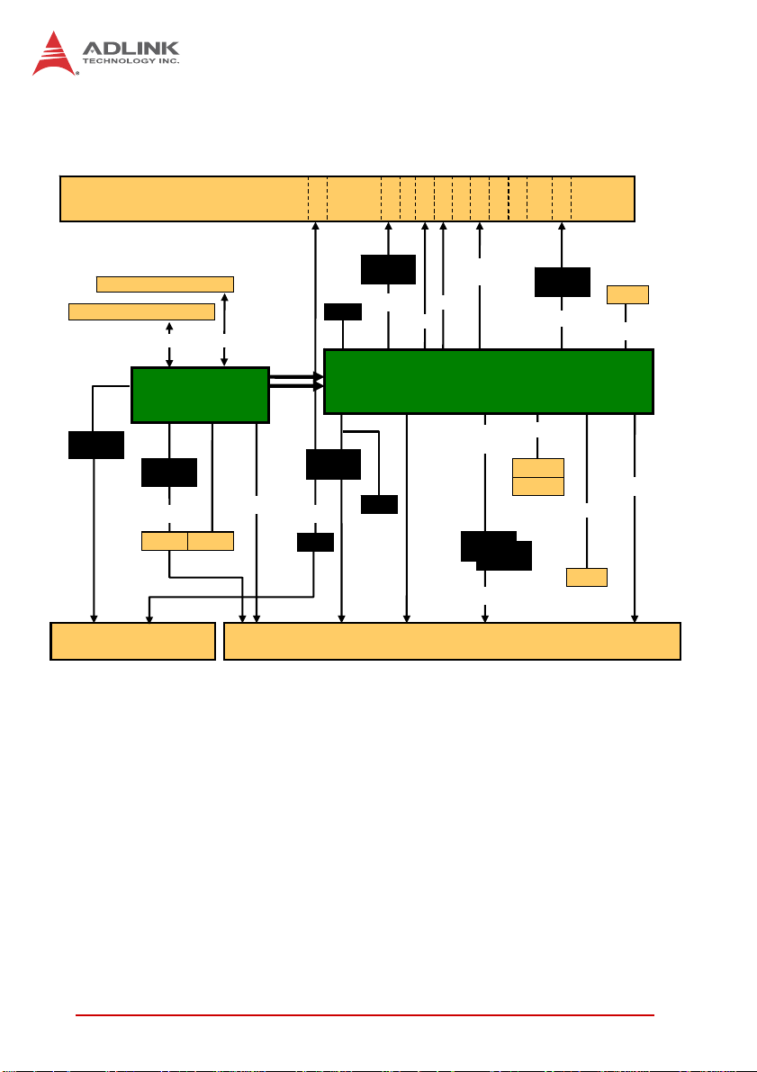
1.3 Block Diagram
Front Panel
COM1
COM1
Intel
BIOS
SIO
82579LM
SPI
LPC
TPM
KB/MS
COM2/3
PCIe x1
ECC SO-CDIMM, max. 8GB
Soldered w/ ECC, max. 8GB
DDR3 1066/1333
PCIe x4
Intel® Core™ i7
w/ ECC
PI7C9X130
PCI 64b/66M
PCIe x4
PI7C9X130
PCI 64b/133M
PMC
Rear I/O
XMC.3
PCIe x8
Gen3
eDP
DMI
FDI
COM6
BMC
IPMB 0/1
J1/J2 J3/J4/J5
Figure 1-1: cPCI-6520 Functional Block Diagram
GbE1
DP-C
DP1
DP-D
DP2
USB 3.0
USB1
USB2
USB3
3x
Intel® BD82QM77 PCH
2x
PCIe x1
Intel
82574
GbE3/4
Intel
82574
2.5” HDD
1x USB 3.0
5x USB 2.0
3x SATA 3Gb/s
HDA
5x GPIO
RTC
RGB,
PCIe x4
SATA0
CFast
GbE2
Intel
82574
PCIe x1
7-pin
SATA2
TMDS/DP-B
SATA1
CF
4Introduction
Page 17

1.4 Product List
Products included in the cPCI-6520 are:
Processor Blade
X cPCI-6520: 4HP width (single-slot) 6U CompactPCI blade
featuring single FCBGA package 3rd Generation Intel®
Core™ i7 processor with quad/dual cores, two channel
DDR3-1066/1333/1600 ECC SDRAM, 2x GbE, 2x DisplayPorts, 3x USB 3.0, 1x RS-232/422/485 serial port in RJ-45
connector, SATA direct connector for onboard 2.5" drive,
onboard CompactFlash socket, PMC/XMC site, optional
CFast support by adapter board.
Rear Transition Module
X cPCI-R6002: 6U 4HP width RTM with DVI-I, 2x COM, 3x
USB, 2x GbE, 2x SATA
X cPCI-R6002D: 6U 8HP width RTM with DVI-I, 2x COM, 5x
USB, 2x GbE, 3x SATA, Mic-in, Line-out, PS/2 KB/MS
X cPCI-R6100: 6U 4HP width RTM with 4x GbE, 4x USB, 2x
SA TA, VGA, PS/2 KB/MS, CF & SD sockets, (Supports only
3x GbE when mating with cPCI-6520)
X cPCI-R6110: 6U 4HP width RTM with 2x GbE, 4x USB, 3x
SATA, VGA, PS/2 KB/MS, CF, & SD sockets
X cPCI-R6200: 6U 8HP width RTM with 2x GbE, 2x COM, 6x
USB, DVI-I (VGA signal only), 3x SATA, Mic-in, Line-out,
PS/2 KB/MS, 8x SAS
X cPCI-R6700: 6U 4HP width RTM with onboard ATI E4690
GPU, 2x DVI-I, 2x GbE, 1x COM, 3x USB, onboard PS/2
KB/MS, 3x SATA
X cPCI-R6700D: 6U 8HP width RTM with onboard ATI E4690
GPU, 2x DVI-I, 2x GbE, 2x COM, 6x USB, Mic-in, Line-in,
Line-out, onboard PS/2 KB/MS, 3x SATA
cPCI-6520
Adapter Kits
X DB-CFast: CFast socket kit for cPCI-6520, including
adapter board and mounting hardware
Introduction 5
Page 18

1.5 Package Contents
The cPCI-6520 is packaged with the following components. If any
of the items on the contents list are missing or damaged, retain the
shipping carton and packing material and contact the dealer for
inspection. Please obtain authorization before returning any product to ADLINK. The packing contents of the cPCI-6520 are
non-standard configurations and may vary depending on customer
requests.
Processor Blade
X cPCI-6520
Z CPU and memory specifications will differ depending on
options selected
Z Thermal module is assembled on the board
X DisplayPort to DVI adapter cable
X RJ-45 to DB-9 cable for RJ-45 COM port
X 2.5" SATA drive mounting kit, including bracket and screws
for 2.5" SATA drive and DB-LSATA adapter card
X ADLINK All-in-One DVD
X User’s manual
Optional Accessories
X DB-CFast: CFast socket kit for cPCI-6520, including
adapter board and mounting hardware
X DP-to-DVI cable: DisplayPort to DVI adapter ca ble
(Part. No. 30-01120-0000)
X DP-VGA cable: DisplayPort to VGA adapter cable
(Part. No. 30-01121-0000)
X DP-to-HDMI cable: DisplayPort to HDMI adapter cable
(Part No. 30-01119-0000)
6Introduction
Page 19

NOTE:
NOTE:
CAUTION:
cPCI-6520
The contents of non-standard cPCI-6520 configurations may
vary depending on the customer requirements.
This product must be protected from static discharge and physical shock. Never remove any of the components except at a
static-free workstation. Use the anti-static bag shipped with the
product when putting the board on a surface. Wear an
anti-static wrist strap properly grounded on one of the system's
ESD ground jacks when installing or servicing system components.
Introduction 7
Page 20

This page intentionally left blank.
8Introduction
Page 21

2 Specifications
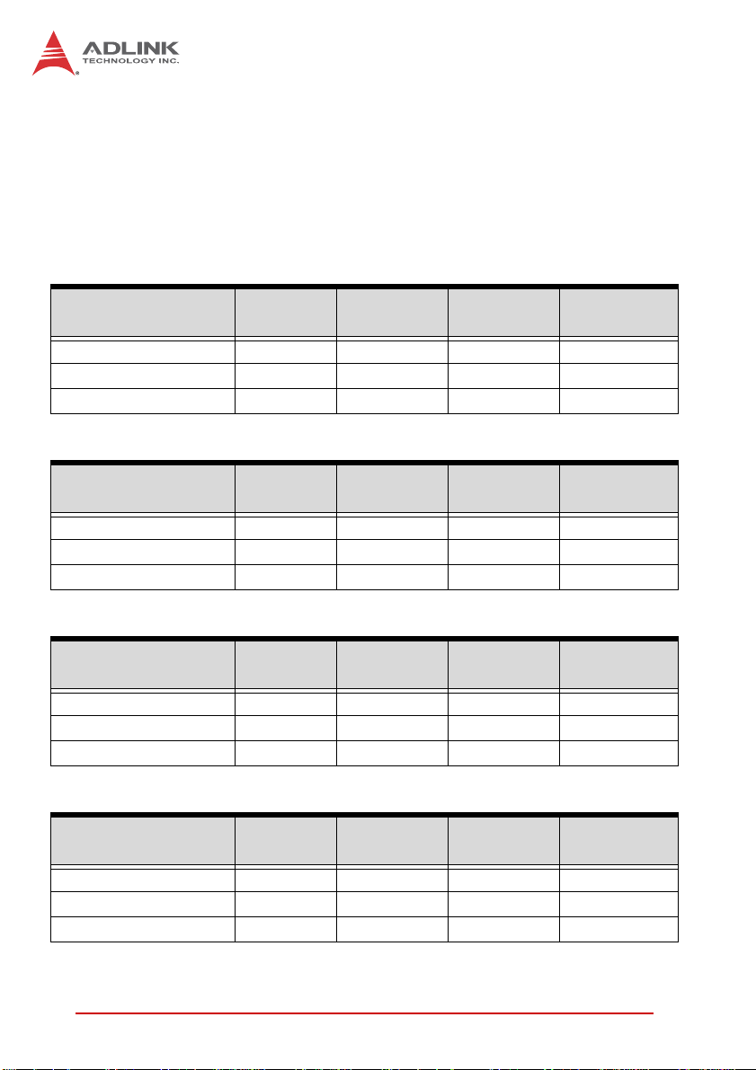
2.1 cPCI-6520 Blade Specifications
cPCI-6520
CompactPCI®
Standards
Mechanical • Standard 6U CompactPCI®
Processor 22nm FCBGA Intel® Core™ i7 Processor
Chipset • Intel® BD82QM77 Platform Controller Hub (PCH)
Memory • Dual channel DDR3-1066/1333/1600 SDRAM with ECC,
CompactPCI
Bus
PMC/XMC • One 32/64-bit, 33/66/133MHz PMC site or PCI-Express x8
Graphics • Integrated in processor
• PICMG® 2.0 CompactPCI® Rev. 3.0
• PICMG® 2.1 Hot Swap Specification Rev.2.0
• PICMG® 2.9 System Management Bus Rev. 1.0
• PCIMG® 2.16 Packet Switching Backplane Rev.1.0
• Board size: 233.35mm x 160mm
• Single-slot width (4HP, 20.32mm)
• CompactPCI® connectors with J1, J2, J3, J4 and J5
• 4-core Intel® Core i7-3615QE Processor, 2.3 GHz, 6MB L3
cache, TDP 45W
• 4-core Intel® Core i7-3612QE Processor, 2.1 GHz, 6MB L3
cache, TDP 35W
• 2-core Intel® Core i7-3555LE Processor, 2.5 GHz, 4MB L3
cache, TDP 25W
• 2-core Intel® Core i7-3517UE Processor, 1.7 GHz, 4MB L3
cache, TDP 17W
• Passive heatsink
total up to 16GB
• One channel in SODIMM sockets up to 8GB
• One channel soldered onboard up to 8GB (dependent on
availability of memory modules and chips)
• PCI 32/64-bit, 33/66MHz; 3.3V, 5V universal V(I/O)
• Supports operation in system slot as master or in peripheral
slot as standalone blade without connectivity to
CompactPCI bus (Satellite mode)
XMC site
• Two dual mode DisplayPorts on front panel with
DVI/VGA/HDMI support by adapter cable
• One DVI, eDP and VGA routed to rear
Table 2-1: cPCI-6520 Blade S pecifications
Specifications 9
Page 22

Gigabit
Ethernet
• One front panel GbE LAN port from Intel® 82579LM PHY
controller and one front panel GbE LAN from Intel 82574
Gigabit Ethernet controller
• Two 10/100/1000BASE-T ports routed to J3 for PICMG
2.16
• Two additional 10/100/1000BASE-T ports from Intel®
82576EB Gigabit Ethernet controllers on RTM (cPCIR6100 or cPCI-R6110)
Serial Ports Up to three 16C550 serial ports
• One DB-9 RS-232/422/485 serial port on front panel
• Two serial ports routed to rear I/O through J3
USB 2.0 • Six USB 2.0 ports routed to J3
USB 3.0 • Three USB 3.0 ports on front panel, one to J5
KB/MS • PS/2 Keyboard/Mouse port to J3
Audio • High Definition Audio signals routed to J3
TPM Atmel AT97SC3204 TPM (upon request)
• Over/Under voltage detection
• Low/High frequency sensor/filter
• Reset filter
• Memory Encryption/Decryption
Storage
Interfaces
• One SATA 6 Gb/s direct connector for 2.5" onboard drive
1
(removable)
1
• Optional CompactFlash socket onboard
• Optional CFast socket onboard via DB-CFAST adapter
board (shares space with 2.5" SATA drive)
• One onboard 7-pin SATA connector
BIOS • AMI EFI BIOS, 64Mbit SPI flash memory
Faceplate I/O • 2x 10/100/1000BASE-T Ethernet ports
• 2x DisplayPorts
• 3x USB 3.0 ports
• 1x RJ-45 RS-232/422/485 port
• PMC/XMC slot
OS
Compatibility
• Microsoft Windows 7 32/64-bit
• Mi crosoft Windows 2008 Server 32-bit, R2 64-bit
• Red Hat Enterprise Linux 6.2 x86 64-bit
• Fedora 16 x86 64-bit
• Wind River VxWorks 6.9 BSP
• Other OS supp ort on request
Table 2-1: cPCI-6520 Blade Specifications
10 Specifications
Page 23

Environmental • Operating Temperature2:
Standard: 0 to 60°C with forced air flow
ETT: -20°C to 70°C with forced air flow (cPCI-ET6520)
EX: -40°C to 85°C with forced air flow (Core™ i7-3555LE &
Core™ i7-3517UE only)
• Storage Temperature: -40°C to 85°C
• Humidity: 95% non-condensing
• Shock: 15G peak-to-peak, 11ms duration, non-operating
•Vibration
3
: Operating 2 Grms, 5-500Hz, each axis w/o hard
drive
EMI • CE EN55022
• FCC Class A
Table 2-1: cPCI-6520 Blade S pecifications
Notes:
1. The SATA direct connector is removable (DB-LSATA) and ca n
be replaced with a CFast socket adapter. A CFast card and
SATA drive cannot be used simultaneously.
2. ADLINK-certified th ermal design. The thermal performance is
dependent on the chassis cooling design. Sufficient forced airflow is required (see 2.4 "Thermal Requirements"). Te mperature limit of optional mass storage devices may affect the thermal specification.
3. The storage device limits the operational vibration. When application requires higher specification for anti-vibration, it is recommended to use a flash storage device.
cPCI-6520
Specifications 11
Page 24

2.2 I/O Connectivity
cPCI-6520 RTM
1
Faceplate Onboard J3/4/5
GbE Y x2 — Y x2
COM Y x1 — Y x2
USB 2.0 —— Y x6
USB 3.0 Y x3 — Y x1
DisplayPort Y x2 — —
eDP Y x1
DVI —— Y x1
VGA —— Y x1
PMC — Y x1 —
XMC Y x1 —
SATA —Y x2
CFast Y x1
2
2
Y x3
CF —Y —
PS/2 KB/MS —— Y x1
HDA —— Y
Status LEDs Y x4 — —
General Purpose LEDs Y x8 — —
Load BIOS Default Button —Y —
Reset Button Y— —
Table 2-2: cPCI-6520 I/O Connectivity
Notes:
1. Signals are passed through to the RTM. Available functions are
dependent on the specific RTM selected.
2. One SATA 6 Gb/s direct connector for 2.5" onboard drive
(shares space with optional DB-CFAST adapter) and one 7-pin
connector.
12 Specifications
Page 25

cPCI-6520
2.3 Power Requirements
In order to guarantee a stable functionality of the system, it is recommended to provide more power than the system requires. An
industrial power supply unit should be able to provide at least
twice as much power as the entire system requires of each
voltage. An ATX pow er supply unit should be able to provide at
least three times as much power as the entire system requires of
each voltage.
The tolerance of the voltage lines described in the CompactPCI
specification (PICMG 2.0 R3.0) is +5%/-3% for 5, 3. 3 V and ±5%
for ±12V. This specification is for power delivered to each slot and
it includes both the power supply and the backplane tolerance.
Voltage
5V +5.0 VDC +5% / -3% 50 mV
3.3V +3.3 VDC +5% / -3% 50 mV
+12V +12 VDC +5% / -5% 240 mV
-12V -12 VDC +5% / -5% 240 mV
V I/O (PCI I/O
Buffer Voltage)
GND
Nominal
Value
+3.3 VDC or
+5 VDC
Tolerance
+5% / -3% 50 mV
Max. Ripple
(P - P)
Specifications 13
Page 26
Power Consumption
This section provides information on the power consumption of the
cPCI-6520 when using Intel® Core™ i7 processors with 4GB DDR31333 soldered memory and onboard ADLINK ASD25 64GB SATA
SSD.
Power consumption at 100% CPU usage was measured by run-
ning Intel Thermal Analysis Tool 4.3.
Quad-Core Intel® Core™ i7-3615QE, 2.3GHz, TDP 45W
OS / Mode
DOS / idle 4.48 2.80 0.19 33.9
Win7 / idle 3.34 2.62 0.20 27.7
Win7 / 100% CPU 13.04 2.8 0.21 77.0
5V Current
(A)
3.3V Current
(A)
12V Current
(A)
Total Power
(W)
Quad-Core Intel® Core™ i7-3612QE, 2.1GHz, TDP 35W
OS / Mode
DOS / idle 4.30 2.79 0.18 32.9
Win7 / idle 3.30 2.55 0.19 27.2
Win7 / 100% CPU 10.21 2.77 0.20 62.6
5V Current
(A)
3.3V Current
(A)
12V Current
(A)
Total Power
(W)
Dual-Core Intel® Core™ i7-3555LE, 2.5GHz, TDP 25W
OS / Mode
DOS / idle 4.25 2.61 0.18 32.0
Win7 / idle 3.23 2.55 0.20 27.0
Win7 / 100% CPU 8.58 2.69 0.20 54.2
5V Current
(A)
3.3V Current
(A)
12V Current
(A)
Total Power
(W)
Dual-Core Intel® Core™ i7-3517UE, 1.7GHz, TDP 17W
OS / Mode
DOS / idle 3.72 2.15 0.18 27.9
Win7 / idle 3.19 2.53 0.18 26.5
Win7 / 100% CPU 6.50 2.68 0.19 43.6
14 Specifications
5V Current
(A)
3.3V Current
(A)
12V Current
(A)
Total Power
(W)
Page 27

3 Functional Description
The following sections describe the cPCI-6520 features and
functions.
3.1 Processors
The 3rd Generation Intel® Core™ i7 Processo r is the next gener ation of 64-bit, multi-core mobile processors built on 22-nanometer
process technology. Based on a new micro-architecture, the processor is designed for a two-chip platform. The two-chip platform
consists of a processor and Platform Controller Hub (PCH). The
platform enables higher performance, lower cost, easier validation, and improved x-y footprint. The processor includes an integrated display engine, processor graphics, integrated memory
controller, and integrated I/O on a single silicon die.
cPCI-6520
Features
Clock 2.3 GHz 2.1 GHz 2.5 GHz 1.7 GHz
Max. Single Core Turbo
Freq.
Last Level Cache 6 MB 6 MB 4 MB 4 MB
No. of Cores/Threads 4/8 4/8 2/4 2/4
Maximum Power (TDP
T
junction,MAX
Memory Type DDR3-1066/
2
Core™
i7-3615QE
3.3 GHz 3.1 GHz 3.2 GHz 2.8 GHz
1
45 W 35 W 25 W 17 W
)
105°C 105°C 105°C 105°C
1333/1600
Core™
i7-3612QE
DDR3-1066/
1333/1600
Core™
i7-3555LE
DDR3-1333/
1600
Core™
i7-3517UE
DDR3-1333/
1600
Notes:
1. The high est expected sustainable power while running known
power intensive applications. TDP is not the maximum power
that the processor can dissipate.
2. The maximum supported operating temperature.
Functional Description 15
Page 28

Supported Technologies
X Intel® Virtualization Technology for Directed I/O (Intel®
VT-d)
X Intel® Virtualization Technology (Intel® VT-x)
X Intel® vPro Technolo gy (I nte l® VT)
X Intel® Trusted Execution Technology (Intel® TXT)
X Intel® Hyper-Threading Technology
X Intel® 64 Architecture
X Intel® Turbo Boost Technology 2.0
X AES New Instructions
X Intel® My WiFi Technology
X Enhanced Intel SpeedStep® Technology
X Thermal Monitoring Technologies
X Intel® Fast Memory Access
X Execute Disable Bit
X Intel® VT-x with Extended Page Tables (EPT)
Interfaces
X Dual channel DDR3 memory with one channel of unbuffered
SODIMM and one channel of soldered SDRAM
X Memory DDR3 data transfer rates of 1333 MT/s and 1600
MT/s
X 64-bit wide channels plus 8-bits of ECC support for each
channel
X The PCI Express lanes are fully-compliant with the PCI
Express Base Specification, Revision 3.0, including support
for 8.0 GT/s transfer speeds.
16 Functional Description
Page 29

cPCI-6520
3.2 Chipset
The cPCI-6520 incorporates the Intel® QM77 Platform Controller
Hub (PCH).
Intel® QM77 Platform Controller Hub
X PCI Express Base Specification, Revision 2.0 support for up
to eight ports with transfer rate up to 5 GT/s
X Supports dual display
X ACPI Power Management Logic Support, Revision 4.0a
X Enhanced DMA controller, interrupt controller, and timer
functions
X Integrated Serial ATA host controllers with independent
DMA operation on up to six ports and SATA 6.0 Gb/s up to
two ports
X Supports USB 2.0, USB 3.0
X USB host interface with two EHCI high-speed USB 2.0 Host
controllers and two rate matching hubs provide support for
up to fourteen USB 2.0 ports
X Integrated 10/100/1000 Gigabit Ethernet MAC with System
Defense
X System Management Bus (SMBus) Specification, Version
2.0 with additional support for I2C devices
X Supports Intel Trusted Execution Technology
X Support vPro Technology
X Support Active Management Technology
X Support AMT Version
X Support Anti-Theft Technology
X Supports Intel® High Definition Audio
X Supports Intel® Rapid Storage Technology
X Supports Intel® Virtualization Technology for Directed I/O
X Low Pin Count (LPC) interface
X Serial Peripheral Interface (SPI) support
Functional Description 17
Page 30

3.3 PMC/XMC Site
The cPCI-6520 supports one PMC or XMC site for front panel I/O
expansion. The PMC site provides a maximum 32/64-bit,
33/66/133MHz PCI bus link using a Pericom PI7C9X130
PCIe-to-PCI-X bridge and PCIe x4 link. The PMC site supports
+3.3V and 5V signaling. The XMC site provides a PCIe x8 lane.
3.4 Intel® Turbo Boost Technology
Intel Turbo Boost Technology is a feature that allows the processor
to opportunistically and automatically run faster than its rated
operating core and/or render clock frequency when there is sufficient power headroom, and the product is within specified temperature and current limits. The Intel Turbo Boost Technology feature
is designed to increase performance of both multi-threaded and
single-threaded workloads. The processor supports a Turbo mode
where the processor can use the thermal capacity associated with
package and run at power levels higher than TDP power for short
durations. This improves the system responsiveness for short,
bursty usage conditions.
Turbo Mode availability is independent of the number of active
cores; however, the Turbo Mode frequency is dynamic and dependent on the instantaneous application power load, the number of
active cores, user configurable settings, operating environment,
and system design. If the power, current, or thermal limit is
reached, the processor will automatically reduce the frequency to
stay with its TDP limit.
3.5 Intel® Hyper Threading Technology
The processor supports Intel® Hyper-Threading Technology
(Intel® HT Technology), that allows an execution core to function
as two logical processors. While some execution resources (such
as caches, execution units, and buses) are shared, each logical
processor has its own architectural state with its own set of general-purpose registers and control registers. This feature must be
enabled using the BIOS and requires operating system support.
18 Functional Description
Page 31

cPCI-6520
3.6 Intel® Active Management Technology
Intel® Active Management Technology (Intel® AMT) is a hardware
based technology for remotely managing and securing PCs
out-of-band. Intel® AMT includes hardware-based remote management, security, power-management, and remote-configuration
features. Intel® AMT allows remote access to a system when traditional techniques and methods are not available.
3.7 TPM
The cPCI-6520 is equipped with the Infineon ATMEL AT97SC3204
Trusted Platform Module (TPM), a security controller with cryptographic functionality that provides users a secure environment in
e-commerce transactions and Internet communications. The key
features provided by the TPM are:
X Hardware hash accelerator for SHA-1 algorithm
X Advanced Crypto Engine (ACE) for asymmetric key oper ations
(up to 2048-bit key length) to make hardware protection.
X Tick counter to extend the time required to decipher the key
X Over/Under-voltage detection to monitor the system stabil-
ity. If the voltage fluctuates dramatically, this function can
block the data transfer and lock the chip.
X Low/High frequency sensor to detect the IC clock fre-
quency. If the frequency fluctuates dramatically, this function can block the data transfer and lock the chip.
X Reset filter to filter reset signal in order to break the time se t
by tick counter is received
X Memory encryption to protect memory
X Physical shield in the IC to protect the die from intruding or
hacking by matching the data transferred on the 2 layer
metal shield on the IC. If the data is not matched, the IC
may be blocked.
3.8 Battery
The cPCI-6520 is provided with a 3.0V “coin cell” lithiu m battery
for the Real Time Clock (RTC). The lithium battery must be
replaced with an identical battery or a battery type recommended
by the manufacturer.
Functional Description 19
Page 32

This page intentionally left blank.
20 Functional Description
Page 33

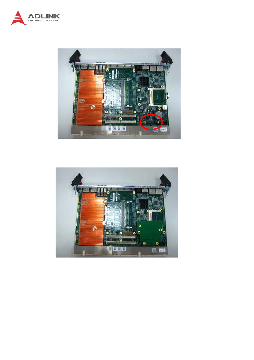
4 Board Interfaces
4.1 cPCI-6520 Board Layout
cPCI-6520
CN13
CN14
CN5
CN6
CN7
CN8
DP1
DP2
SW13
SW_COMPW1
Onboard Memory
CN3
SW_COMDEG1
CN1
SW_PMC1
SW7
BT2
SW1
J N1 JN3
CN10
J5
CN9
J4
SW_VIO1
SW_MOD1
SW_IPMCDEG1
J N2 JN4
CN2
J3
J2
J1
BT2 Battery JN1/2/3/4 PMC connectors
CN1 SODIMM Socket SW1 BI OS default button
CN2 XMC connector SW12 COM RS-232/422/485
CN5 COM1 port SW13 Reserved
CN6/7/8 USB 3.0 ports SW_COMDEG1 Reserved
CN9 SATA connector SW_COMPW1 Reserved
CN10 SA TA 7-pin connector SW_IPMCDEG1 Reserved
CN13/CN14 GbE ports SW_MOD1 Reserved
DP1/2 DisplayPorts SW_PMC1 PMC frequency setting
J1/J2/J3/J5 cPCI connectors SW_VIO1 PMC power setting
Figure 4-1: cPCI-6520 Board Layout
Board Interfaces 21
Page 34

4.2 cPCI-6520 Assembly Layout
DB-LSATA
Onboard
2.5" Drive
Figure 4-2: cPCI-6520 Assembly Layout
22 Board Interfaces
Page 35

4.3 cPCI-6520 Front Panel
p
cPCI-6520
GbE 1/ 2 USB 3. 0
COM1
Pur
General
ose LEDs
PMC/XMC
Figure 4-3: cPCI-6520 Front Panel
Status LEDs
LED Color Condition Indication
Power
HotSwap
WDT
HDD
Green
Blue
Red
Amber
OFF System is off
ON System is on
Blink
Fail to power on
(payload power failure)
OFF Handles closed, System is on
Fast Blink
ON
Preparing to shut down system
(LED: 0.1s on, 0.9s off.)
Handles open and blade ready
to be removed
Voltages out of tolerance:
Slow Blink
3.3V, 5V, 12V, 1.5V over ±5%
(LED 2s on, 1s off)
OFF No Watchdog event
ON Watchdog event alert
OFF No drive activity
Blink
SATA, CF data read/write in
process
Reset
Button
DisplayPort
Status
LEDs
General Purpose LEDs
In default mode, these eight LEDs display the POST codes output
to Port 80h during system boot up. For example, if the Bit7 > Bit0
output is “01110101”, then the port 80h output is “75h” (See
“Checkpoints & Beep Codes” on page 105).
Board Interfaces 23
Page 36

4.4 Connector Pin Assignments
See “cPCI-6520 Board Layout” on page 21 for connector locations.
Front Panel Connectors
Gigabit Ethernet Connectors (RJ-45)
Pin # GbE Signal
1LAN_TX0+
2 LAN_TX03LAN_TX1+
4LAN_TX2+
5 LAN_TX26 LAN_TX17LAN_TX3+
8LAN_TX3+
Speed Activity
81
Status
Network link is not established
or system powered off
10 Mbps
100 Mbps
1000 Mbps
24 Board Interfaces
Link OFF ON
Active OFF Blinking
Link Green ON
Active Green Blinking
Link Amber ON
Active Amber Blinking
Speed LED
(Green/Amber)
OFF OFF
Activity LED
(Amber)
Page 37

COM1 (RJ-45)
Pin # RS-232 RS-422 RS-485
1 DCD# TX- Data2RTS# — —
3DSR# — —
4TXD RX+ —
5 RXD TX+ Data+
6GND — —
7CTS# — —
8DTR#L RX- —
COM1 RJ-45 to DB-9 Cable
Pin # RS-232 RS-422 RS-485
1 DCD# TX- Data2 RXD TX+ Data+
3TXD RX+ —
4DTR#L RX- —
5GND — —
6DSR# — —
7RTS# — —
8CTS# — —
9— — —
cPCI-6520
18
6
1
5
Board Interfaces 25
Page 38

USB 3.0 Connectors
Pin # Signal Name
1VCC
2 Data3 Data+
4GND
5RX_N
6RX_P
7GND
8TX_N
9TX_P
DisplayPort Connectors (DP1, DP2)*
Pin # Signal Pin # Signal
1 CN_DP0_P 2 Ground
3 CN_DP0_N 4 CN_DP1_P
5 Ground 6 CN_DP1_N
7 CN_DP2_P 8 Ground
9 CN_DP2_N 10 CN_DP3_P
11 Ground 12 CN_DP3_N
13 CN_CAD-L 14 CN_CEC
15 CN_AUX_P 16 Ground
17 CN_AUX_N 18 DDP_HPD
19 Ground 20 P3V3
1
2
19
20
*If one of the front panel DisplayPorts is converted to DVI or
HDMI, the cPCI-6520 can support only two independent dis-
NOTE:
NOTE:
plays via the front panel and the rear I/O VGA output i s disable d.
26 Board Interfaces
Page 39

Onboard Connectors
SATA Connector (CN10)
Pin # Signal
1GND
2TXP
3TXN
4GND
5RXN
6RXP
7GND
SATA Connector on DB-LSATA
Pin # Signal
S1 GND
S2 TX+
S3 TXS4 GND
S5 RXS6 RX+
S7 GND
P1 NC
P2 NC
P3 NC
P4 GND
P5 GND
P6 GND
P7 5V
P8 5V
P9 5V
P10 GND
P11 Reserved
P12 GND
P13~P15 12V
cPCI-6520
1
7
S1
Signal
S7
P1
Power
P15
Board Interfaces 27
Page 40

CFast Socket (on DB-CFast)
Pin # Signal Name
Ground S1
SATA_TX-P S2
SATA_TX-N S3
Ground S4
SATA_RX-N S5
SATA_RX-P S6
Ground S7
CFast_CDI P1
Ground P2
NC P3
NC P4
NC P5
NC P6
Ground P7
CFast_LED1 P8
CFast_LED2 P9
NC P10
NC P11
NC P12
P3V3 P13
P3V3 P14
Ground P15
Ground P16
CFast_CDO P17
24
1
S1P1
28 Board Interfaces
Page 41

DB-LSAT A Connector (CN9)
cPCI-6520
Signal Name Pin # Pin # Signal Name
GND 1 2 GND
GND 3 4 GND
GND 5 6 GND
GND 7 8 GND
GND 9 10 GND
GND 11 12 GND
GND 13 14 GND
GND 15 16 GND
GND 17 18 GND
GND 19 20 GND
GND 21 22 GND
GND 23 24 GND
GND 25 26 GND
GND 27 28 GND
GND 29 30 GND
P3V3 31 32 P5V
P3V3 33 34 P5V
P3V3 35 36 P5V
P3V3 37 38 P5V
NC 39 40 P12V
CFAST_CDI 41 42 P12V
CFAST_CDO 43 44 P12V
GND 45 46 GND
GND 47 48 SATA_TXN0
GND 49 50 SATA_TXP0
SATA_RXN0 51 52 GND
SATA_RXP0 53 54 GND
GND 55 56 NC
GND 57 58 GND
GND 59 60 GND
59 60
1 2
Board Interfaces 29
Page 42

PMC Connector (JN1, JN2, JN3, JN4)
Pin# JN1 Signal JN2 Signal JN3 Signal JN4 Signal
1 PMC_TCK P12V NC PIO1
2 N12V* PMC_TRST-L GND PIO2
3 GND PMC_TMS GND PIO3
4 PCIX_INTA-L NC (PMC_TDO) PCIX_CBE-L7 PIO4
5 PCIX_INTB-L PMC_TDI PCIX_CBE-L6 PIO5
6 PCIX_INTC-L GND PCIX_CBE-L5 PIO6
7 PMC_MOD-L1 GND PCIX_CBE-L4 PIO7
8P5V NC GND PIO8
9 PCIX_INTD-L NC PMC_VIO PIO9
10 NC NC PCIX_PAR64 PIO10
11 GND PMC_MOD-L2 PCIX_AD63 PIO11
12 P3V3_PMCAUX P3V3 PCIX_AD62 PIO12
13 CLK66_PCIX_PMC PMC_RST-L PCIX_AD61 PIO13
14 GND PMC_MOD-L3 GND PIO14
15 GND P3V3 GND PIO15
16 PCIX_GNT-L0 PMC_MOD-L4 PCIX_AD60 PIO16
17 PCIX_REQ-L0 PMC_PME-L PCIX_AD59 PIO17
18 P5V GND PCIX_AD58 PIO18
19 PMC_VIO PCIX_AD30 PCIX_AD57 PIO19
20 PCIX_AD31 PCIX_AD29 GND PIO20
21 PCIX_AD28 GND GND PIO21
22 PCIX_AD27 PCIX_AD26 PCIX_AD56 PIO22
23 PCIX_AD25 PCIX_AD24 PCIX_AD55 PIO23
24 GND PCIX_AD23 PCIX_AD54 PIO24
25 GND PMC_IDSEL PCIX_AD53 PIO25
26 PCIX_CBE-L3 PCIX_AD23 GND PIO26
27 PCIX_AD22 P3V3 GND PIO27
28 PCIX_AD21 PCIX_AD20 PCIX_AD52 PIO28
29 PCIX_AD19 PCIX_AD18 PCIX_AD51 PIO29
30 P5V GND PCIX_AD50 PIO30
31 PCIX_FRAME-L PCIX_AD16 PCIX_AD49 PIO31
32 PCIX_AD17 PCIX_CBE-L2 GND PIO32
6364
12
*Note: -12V signal not supported on JN1 pin 2. Contact ADLINK for more
information.
30 Board Interfaces
Page 43

Pin# JN1 Signal JN2 Signal JN3 Signal JN4 Signal
33 PCIX_FRAME-L GND GND PIO33
34 GND NC PCIX_AD48 PIO34
35 GND PCIX_TRDY-L PCIX_AD47 PIO35
36 PCIX_IRDY-L P3V3 PCIX_AD46 PIO36
37 PCIX_DEVSEL-L GND PCIX_AD45 PIO37
38 P5V PCIX_STOP-L GND PIO38
39 PCIX_PCIXCAP PCIX_PERR-L GND PIO39
40 PCIX_LOCK-L GND PCIX_AD44 PIO40
41 NC P3V3 PCIX_AD43 PIO41
42 NC PCIX_SERR-L PCIX_AD42 PIO42
43 PCIX_PAR PCIX_CBE-L1 PCIX_AD41 PIO43
44 GND GND GND PIO44
45 PMC_VIO PCIX_AD14 GND PIO45
46 PCIX_AD15 PCIX_AD13 PCIX_AD40 PIO46
47 PCIX_AD12 PCIX_M66EN PCIX_AD39 PIO47
48 PCIX_AD11 PCIX_AD10 PCIX_AD38 PIO48
49 PCIX_AD9 PCIX_AD8 PCIX_AD37 PIO49
50 P5V P3V3 GND PIO50
51 GND PCIX_AD7 GND PIO51
52 PCIX_CBE-L0 NC PCIX_AD36 PIO52
53 PCIX_AD6 P3V3 PCIX_AD35 PIO53
54 PCIX_AD5 NC PCIX_AD34 PIO54
55 PCIX_AD4 NC PCIX_AD33 PIO55
56 GND GND GND PIO56
57 PMC_VIO NC GND PIO57
58 PCIX_AD3 NC PCIX_AD32 PIO58
59 PCIX_AD2 GND NC PIO59
60 PCIX_AD1 NC NC PIO60
61 PCIX_AD0 PCIX_ACK64-L NC PIO61
62 P5V P3V3 GND PIO62
63 GND GND GND PIO63
64 PCIX_REQ64-L NC NC PIO64
PMC Connector Pin Definition (cont’d)
cPCI-6520
Board Interfaces 31
Page 44

XMC Connector (CN2)
F1 F19
A1
A19
Pin# A B C D E F
1
2
3
4
5
6
7
8
9
10
11
12
13
14
15
16
17
18
19
RXP RXN 3.3V NC NC VPWR
GND GND Not used GND GND PCIE_RST-L
NC NC 3.3V NC NC VPWR
GND GND Not used GND GND Not used
NC NC 3.3V NC NC VPWR
GND GND Not used GND GND +12V
NC NC 3.3V NC NC VPWR
GND GND Not used GND GND -12V
NC NC Not used NC NC VPWR
GND GND Not used GND GND GA0
TXP TXN Not used NC NC VPWR
GND GND GA1 GND GND Not used
NC NC 3.3V NC NC VPWR
GND GND GA2 GND GND Not used
NC NC Not used NC NC VPWR
GND GND Not used GND GND Not used
NC NC Not used NC NC NC
GND GND Not used GND GND Not used
CK-P CK-N Not used Not used Not used Not used
32 Board Interfaces
Page 45

cPCI-6520
CompactPCI J1 Connector Pin Assignment
Pin Z A B C D E F
25 GND +5V REQ64# ENUM# +3.3V +5V GND
24 GND AD1 +5V V(I/O) AD0 ACK64# GND
23 GND P3V3 CPCI_AD4 CPCI_AD3 P5V CPCI_AD2 GND
22 GND CPCI_AD7 GND P3V3 CPCI_AD6 CPCI_AD5 GND
21 GND P3V3 CPCI_AD9 CPCI_AD8 CPCI_M66EN CPCI_CBE-L0 GND
20 GND CPCI_AD12 GND VIO CPCI_AD11 CPCI_AD10 GND
19 GND P3V3 CPCI_AD15 CPCI_AD14 GND CPCI_AD13 GND
18 GND CPCI_SERR-L GND P3V3 CPCI_PAR CPCI_CBE-L1 GND
17 GND P3V3 IPMB_CLK IPMB_DAT GND CPCI_PERR-L GND
16 GND CPCI_DEVSEL-L GND VIO CPCI_STOP-L CPCI_LOCK-L GND
15 GND P3V3 CPCI_FRAME-L CPCI_IRDY-L NC CPCI_TRDY-L GND
12-14 GND Key Area Key
11 GND CPCI_AD18 CPCI_AD17 CPCI_AD16 GND CPCI_CBE-L2 GND
10 GND CPCI_AD21 GND P3V3 CPCI_AD20 CPCI_AD19 GND
9 GND CPCI_CBE-L3 NC CPCI_AD23 GND I CPCI_AD22 GND
8 GND CPCI_AD26 GND VIO CPCI_AD25 CPCI_AD24 GND
7 GND CPCI_AD30 CPCI_AD29 CPCI_AD28 GND CPCI_AD27 GND
6 GND CPCI_REQ-L0 GND P3V3 CPCI_CLK0 CPCI_AD31 GND
5 GND NC NC CPCI_RESET-L GND CPCI_GNT-L0 GND
4 GND P5V_IPMB CPCI_HEALTHY-L VIO NC NC GND
3 GND CPCI_IRQA-L CPCI_IRQB-L CPCI_IRQC-L P5V CPCI_IRQD-L GND
2 GND cPCI_TCK-L P5V cPCI_TMS-L NC cPCI_TDI-L GND
1 GND P5V N12V cPCI_TRST-L P12V P5V GND
Board Interfaces 33
Page 46

CompactPCI J2 Connector Pin Assignment
Pin Z A B C D E F
22 GND GA4 GA3 GA2 GA1 GA0 GND
21 GND CLK6 GND NC NC NC GND
20 GND CLK5 GND NC GND NC GND
19 GND GND GND NC NC NC GND
18 GND NC NC NC GND NC GND
17 GND NC GND RSTBTN# REQ6#
16 GND NC NC DEG# GND NC GND
15 GND NC GND FAL# REQ5# GNT5# GND
14 GND AD35 AD34 AD33 GND AD32 GND
13 GND AD38 GND V(I/O) AD37 AD36 GND
12 GND AD42 AD41 AD40 GND AD39 GND
11 GND AD45 GND V(I/O) AD44 AD43 GND
10 GND AD49 AD48 AD47 GND AD46 GND
9 GND AD52 GND V(I/O) AD51 AD50 GND
8 GND AD56 AD55 AD54 GND AD53 GND
7 GND AD59 GND V(I/O) AD58 AD57 GND
6 GND AD63 AD62 AD61 GND AD60 GND
5 GND CBE5# GND V(I/O) CBE4# PAR64 GND
4 GND V(I/O) NC CBE7# GND CBE6# GND
3 GND CLK4 GND GNT3# REQ4# GNT4# GND
2 GND CLK2 CLK3 SYSEN# GNT2# REQ3# GND
1 GND CLK1 GND REQ1# GNT1# REQ2# GND
GNT6#
GND
34 Board Interfaces
Page 47

cPCI-6520
CompactPCI J3 Pin Assignment
Pin Z A B C D E F
19 GND P5V P5V P12V P5V P5V GND
18 GND LAN3_TXD1+ LAN3_TXD0- GND LAN3_TXD2+ LAN3_TXD2- GND
17 GND LAN3_TXD1+ LAN3_TXD1- GND LAN3_TXD3+ LAN3_TXD3- GND
16 GND LAN4_TXD0+ LAN4_TXD0- GND LAN4_TXD2+ LAN4_TXD2- GND
15 GND LAN4_TXD1+ LAN4_TXD1- GND LAN4_TXD3+ LAN4_TXD3- GND
14 GND USB-OC5# USB-OC6# USB-OC7# USB-OC8# USB-OC9# GND
13 GND USB-P8+ USB-P8- GND USB-P9+ USB-P9- GND
12 GND USB-P6+ USB-P6- GND USB-P7+ USB-P7- GND
11 GND USB-P4+ USB-P4- GND USB-P5+ USB-P5- GND
10 GND USB-OC4# RGB-DDCCLK RGB-DDCDAT RGB-HSYNC RGB-VSYNC GND
9GNDCOM2-CTS# COM2-RI# RGB-BLUE RGB-RED RGB-GREEN GND
8GND COM2-RX COM2-TX COM2-DTR# COM2-DSR# COM2-RTS# GND
7GND COM3-TX COM3-RX COM2-DCD# IPMB_CLK IPMB_DAT GND
6GND SATA-RX4+ SATA-RX4- GND SATA-RX3+ SATA-RX3- GND
5 GND GND GND NC GND GND GND
4GND SATA-TX4+ SATA-TX4- GND SATA-TX3+ SA TA-TX3- GND
3GND KBDATA KBCLK NC MSDATA MSCLK GND
2GNDHDA_SDIN1 HDA_SDIN2 NC HDA_DOCK_EN# HAD_DOCK_RST# GND
1GND HDA_RST# HDA_SYNC HDA_BIT_CLK HDA_SDOUT HDA_SDIN0 GND
High Definition Audio
Keyboard/Mouse
Serial A TA
Serial ports
USB 2.0 ports
Ethernet ports
RGB
Board Interfaces 35
Page 48

CompactPCI J4 Connector Pin Assignment
Pin Z A B C D E F
25 GND PMC IO:P1 PMC IO:N1 NC PMC IO:P2 PMC IO:N2 GND
24 GND PMC IO:P3 PMC IO:N3 NC PMC IO:P4 PMC IO:N4 GND
23 GND NC NC NC NC NC GND
22 GND PMC IO:P5 PMC IO:N5 NC PMC IO:P6 PMC IO:N6 GND
21 GND PMC IO:P7 PMC IO:N7 NC PMC IO:P8 PMC IO:N8 GND
20 GND NC NC NC NC NC GND
19 GND PMC IO:17 PMC IO:19 NC PMC IO:18 PMC IO:20 GND
18 GND PMC IO:21 PMC IO:23 NC PMC IO:22 PMC IO:24 GND
17 GND NC NC NC NC NC GND
16 GND PMC IO:25 PMC IO:27 NC PMC IO:26 PMC IO:28 GND
15 GND PMC IO:29 PMC IO:31 NC PMC IO:30 PMC IO:32 GND
12-14 GND Key Area Key
11 GND PMC IO:33 PMC IO:35 NC PMC IO:34 PMC IO:36 GND
10 GND PMC IO:37 PMC IO:39 NC PMC IO:38 PMC IO:40 GND
9 GND NC NC NC NC NC GND
8 GND PMC IO:41 PMC IO:43 NC PMC IO:42 PMC IO:44 GND
7 GND PMC IO:45 PMC IO:47 NC PMC IO:46 PMC IO:48 GND
6 GND NC NC NC NC NC GND
5 GND PMC IO:49 PMC IO:51 NC PMC IO:50 PMC IO:52 GND
4 GND PMC IO:53 PMC IO:55 NC PMC IO:54 PMC IO:56 GND
3 GND NC NC NC NC NC GND
2 GND PMC IO:57 PMC IO:59 NC PMC IO:58 PMC IO:60 GND
1 GND PMC IO:61 PMC IO:63 NC PMC IO:62 PMC IO:64 GND
36 Board Interfaces
Page 49

cPCI-6520
CompactPCI J5 Pin Assignment
Pin Z A B C D E F
22 GND Power LED
21 GND eDP_TX1+ eDP_TX1- GND eDP_TX3+ eDP_TX3- GND
20 GND eDP_TX0+ eDP_TX0- GND eDP_TX2+ eDP_TX2- GND
19 GND GND GND GND eDP_AUX+ eDP_AUX- GND
18 GND NC NC GND NC NC GND
17 GND NC NC GND NC NC GND
16 GND GND GND eDP_HPD# GND GND GND
15 GND NC NC GND SATA-RX5+ SATA-RX5- GND
14 GND NC NC GND SATA-TX5+ SATA-TX5- GND
13 GND LAN2_100# LAN3_100# NC LAN3_1G# LAN2_1G# GND
12 GND DVI_DATA DVI_CLK DVI_HTPLG NC NC GND
11 GND TDC2+ TDC2- GND TLC+ TLC- GND
10 GND TDC0+ TDC0- GND TDC1+ TDC1- GND
9GND GPIO1 GPIO2 GPIO3 GPIO4 GPIO5 GND
8GNDUSB3.0_SSTX3+ USB3.0_SSTX3- GND USB3.0_SSRX3+ USB3.0_SSRX3- GND
7 GND GND GND RTC GND GND GND
6GND PCIE-CLK+ PCIE-CLK- GND RESET# SATA_LED GND
5 GND GND GND GND GND GND GND
4GND PCIE-TX3+ PCIE-TX3- GND PCIE-RX3+ PCIE-RX3- GND
3GND PCIE-TX2+ PCIE-TX2- GND PCIE-RX2+ PCIE-RX2- GND
2GND PCIE-TX1+ PCIE-TX1- GND PCIE-RX1+ PCIE-RX1- GND
1GND PCIE-TX0+ PCIE-TX0- GND PCIE-RX0+ PCIE-RX0- GND
LAN2_LINK_ACT# LAN2_VCC_TERM LAN3_LINK_ACT# LAN3_VCC_TERM
GND
PCI Express x4
GPIO
Serial ATA
DVI
USB 3.0 ports
Ethernet ports
eDP
If one of the front panel DisplayPorts is converted to DVI or
HDMI, the cPCI-6520 can support only two independent dis-
NOTE:
NOTE:
plays via the front panel and the rear I/O display output is disabled.
Board Interfaces 37
Page 50

4.5 Switches and Buttons
See “cPCI-6520 Front Panel” on page 23 and “cPCI-6520 Board
Layout” on page 21 for switch locations.
System Reset Button
The cPCI-6520 has a system reset button on the front panel.
See “cPCI-6520 Front Panel” on page 23 for the button location.
Load BIOS Default Button (SW1)
Press switch SW1 to load the default BIOS settings.
COM1 Mode Switch (SW12)
Switch SW12 sets the mode of the COM1 port on the front panel.
ON
1 2
Mode 1 2
RS-232 (default) ON OFF
RS-422 ON ON
RS-485 OFF ON
38 Board Interfaces
Page 51

cPCI-6520
IPMC Mode Switch (SW_MOD1)
Switch SW_MOD1 is a multi purpose switch that allows users to
define the blade operating mode. All are set to OFF by default.
ON
1 2
3 4
Pin# Status Description
1OFF
Reserved
When the system does not include a Chassis Management
OFF
Module (CMM), set this pin to OFF to allow IPMI to run in
2
3OFF
4
"without CMM mode" (default).
When the system includes a CMM, set this pin to ON to allow
ON
IPMI to run in "with CMM mode".
Reserved
The power on/off is state is controlled by the ejector handle
OFF
state. Do not change the default setting (OFF).
ON
Force the ejector handle state to "closed".
Board Interfaces 39
Page 52

PMC Frequency Switch (SW_PMC1)
Switch SW_PMC1 sets the frequency and mode of the PMC
slot. All are set to OFF by default..
ON
1 2
3 4
Pin# Status Function
OFF
1
OFF
2
OFF
3
OFF PCI-X 133 MHz (default)
4
64-bit bus (default)
ON
32-bit bus
PCI 33 MHz (default).
PCI 66 MHz
ON
PCI-X mode (default)
PCI mode
ON
PCI-X 100M Hz
PMC VIO Function (SW_VIO1)
Switch SW_VIO1 sets the VIO signal voltage of the PMC slot.
ON
Status Function
OFF (short 1-2) 5V
ON (short 2-3) 3.3V (Default)
1
OFF
40 Board Interfaces
Page 53

cPCI-6520
SW_IPMCDEG1
Switch SW_IPMCDEG1 is for debugging purposes and should
be left in the default setting of “All OFF”.
1
2
ON
Pin Function
1, 4 ON Force power on
2, 3 ON Disable IPMC latch
All ON Disable IPMC
All OFF IPMC enable (Default)
When the cPCI-6520 is mated with the cPCI-R6700, it is necessary to set pins 1, 4 on the SW_IPMCDEG1 to ON (Force
NOTE:
NOTE:
power on).
Reserved Switches
Button SW13 and switches SW_COMDEG1, SW_COMPW1
and SW_IPMCDEG1 are reserved and their settings should not
be altered unless instructed by ADLINK. The default settings
are as follows:
SW_COMDEG1: 1, 2 ON; 3, 4 OFF
SW_COMPW1: ON (short 2-3)
Board Interfaces 41
Page 54

This page intentionally left blank.
42 Board Interfaces
Page 55

5 Getting Started
This chapter describes the installation of the following component s
to the cPCI-6520 and rear transition modules:
X CompactFlash card
X 2.5” SATA hard drive
X CFast card
X PMC/XMC module installation
5.1 CPU and Heatsink
The cPCI-6520 comes with CPU(s) and heatsink pre-installed.
Removal of heatsink/CPU by users is not recommended. Please
contact your ADLINK service representative for assistance.
5.2 CompactFlash Card Installation
The cPCI-6520 series provides space to install a CompactFlash
card. Follow the instructions below to install a CompactFlash card
to the cPCI-6520.
cPCI-6520
Getting Started 43
Page 56

Installing a CF card
1. A CompactFlash can be installed in the location marked
below.
2. Turn the blade over (solder side up). Unscrew the two
screws securing the CompactFlash retention bracket as indicated below and remove the CompactFlash retention holder.
44 Getting Started
Page 57

cPCI-6520
3. Turn the blade over (component side up), then align and
insert the CompactFlash card into the slot until it is properly seated.
4. 4.Align the retention bracket to the screw holes. Turn th e
blade over (solder side up) and secure CompactFlash
card retention bracket to the blade wit h two screws indicated as below.
Getting Started 45
Page 58

5. The CompactFlash card installation is completed.
Removing a CF card with SATA Drive installed
To remove a CompactFlash card, reverse the above steps. If CompactFlash card removal is required when a SATA drive is installed,
follow the instructions below.
1. Remove the CompactFlash bracket without removing
the drive bracket by first turning over the cPCI-6520
blade and unscrewing the CompactFlash bracket as
shown below.
46 Getting Started
Page 59

cPCI-6520
2. Remove the screw securing the CompactFlash bracket
to the drive assembly as marked below.
3. Remove the CompactFlash card.
Getting Started 47
Page 60

5.3 SATA Drive Installation
The cPCI-6520 provides space to install a slim type 2.5” SATA
drive.
Installing a SATA Drive - cPCI-6520
1. Locate the LB-LSATA daughter board in the package
and connect it to slim type 2.5"drive.
2. Find the drive bracket in the package and orient the drive
and bracket as shown below.
48 Getting Started
Page 61

cPCI-6520
3. Secure the drive to the bracket by fastening the four
screws provided in the package in the locations marked
below.
4. Align and assemble the connector on the DB-LSATA to
onboard SATA connec to r ( CN9 ) by fa st en ing t wo screws
marked as below.
Getting Started 49
Page 62

5. Secure the drive bracket by securing a screw at the CF
bracket through to the drive bracket shown as below.
6. Turn the blade over and secure two screws marked as below.
50 Getting Started
Page 63

cPCI-6520
5.4 PMC/XMC Installation
The cPCI-6520 series provides space to install a PMC or XMC
module.
1. A PMC/XMC mezzanine card can be installed on the
cPCI-6520 in the location indicated below.
2. Remove the PMC filler plate on the front panel.
Getting Started 51
Page 64

3. Align the connectors on the PMC/XMC module to the
PMC/XMC connectors on cPCI-6520 blade. Press down
to secure the PMC/XMC module to the cPCI-6520.
4. Remove the black plastic caps securing the mounting
screws to the front panel.
52 Getting Started
Page 65

cPCI-6520
5.5 CFast Card installation
The cPCI-6520 Series provides space to install a CFast card
(optional accessory P/N: 91-37572-000E; please contact your
ADLINK representative for availability). The CFast card space is
shared with the 2.5" SATA drive and both cannot be installed
simultaneously.
1. Prepare a CFast adapter board.
2. Align and insert the CFast card into the CFast adapter
board.
Getting Started 53
Page 66
3. 3.The CFast adapter with card can be installed at the
SATA connector location as indicated below.
4. 4.Flip the CFast adapter so that the card is face down.
Align and connect the CFast adapter to the onboard
SATA connector until it is properly seated.
54 Getting Started
Page 67

cPCI-6520
5. 5.Se cure the CFast adapter with two screws as shown
below.
Getting Started 55
Page 68

This page intentionally left blank.
56 Getting Started
Page 69

6 Driver Installation
The cPCI-6520 drivers are available from the ADLINK All-In-One
DVD at X:\cPCI\cPCI-6520\, or from the ADLINK website
(http://www.adlinktech.com). ADLINK provides validated drivers for Windows XP Professional and Windows 7. We recommend
using these drivers to ensure compatibility. The VxWorks BSP can
also be downloaded from the cPCI-6520 product page on the
ADLINK website.
1. Install the Windows operating system before installing
any driver. Most standard I/O device drivers are installed
during Windows installation.
2. Install the chipset driver by extracting and running the
program in ...\Chipset\ Intel_Chipset_Device
_Software_AllOS_9-3-0-1020.zip.
3. Install the Microsoft .Net Framework by extracting and
running the program in …\Chipset\
Microsoft_Net_Framework_All_WinOS_4-0.zip.
4. Install the graphics driver and utilities by extracting and
running the program in ...\Graphics\
Intel_HD_Graphics_Family_WIN7_32_15-26-9-2712.zip
.
cPCI-6520
5. Install the LAN driver by extracting and running the pro-
gram in …\LAN\ Intel_Network_Adapter_WIN7_32
_v17-0.zip.
6. Install the Rapid Storage Technology Interface by
extracting and running the program in …\AHCI\
Intel_Rapid_Storage_Technology_All_WinOS_v8-7-0
-1007.zip.
7. Install the USB 3.0 driver by extracting and running the
program in …\USB\Intel_USB30_eXtensible_Host
_Controller_Driver_1-0-4-225.zip.
8. Install the AHCI/RAID driver by extracting and running
the program in …\AHCI\ Intel_RST_Driver
_Files_F6_Install_32bit_11-1-0-1006.zip.
Driver Installation 57
Page 70

9. Install the TPM utilities by extracting and running the
program in …\TPM\ Atmel_TPM_Dvr_WinXP_32_64
_4-0-0-msi.zip.
10.Install the audio drivers and utility by extracting and running the program in …\Audio\Realtek_High_Definition
_Audio_Win7_32_6-0-1-6602.zip.
11. Install the Intel Management Engine Interface driver for
iAMT support by extracting and running the program in
...\Chipset\ Intel_Management_Engine_Interface
_AllOS__8-0-10-1464.zip.
58 Driver Installation
Page 71

7 Utilities
7.1 Watchdog Timer
This section describes the operation of the cPCI-6520’s watchdog
timer (WDT). The primary function of the WDT is to monitor the
cPCI-6520's operation and to reset the system if a software application fails to function as prog rammed. The following WDT functions may be controlled using a software application:
X enabling and disabling
X reloading timeout value
The cPCI-6520 custom WDT circuit is implemented using the
internal IO of the Winbond SuperIO W83627UHG which is at 2 Eh
of LPC. The basic functions of the WDT include:
X Starting the timer countdown
X Enabling or disabling WDT
X Enabling or disabling WDT countdown LED ON
X Reloading the timeout value to keep the watchdog from tim-
ing out
X Setting the range of the timeout period from 1 to 15300 seconds
X Sending a RESET signal to the system when the watchdog
times out
cPCI-6520
Using the Watchdog in an Application
The following section describes using the WDT functions in an
application. The WDT reset function is explained in the previous
section. This can be controlled through the registers in the cPCI6520's SuperIO.
An application using the reset fe ature enab les the watch dog func tion, sets the count-down period, and reloads the timeout value
periodically to keep it from resetting the system. If the timer countdown value is not reloaded, the watchdog resets the system hardware after its counter reaches zero.
ADLINK provides a demo DOS utility in the ADLINK All-In-One
CD. You can find it in the following directory: X:\cPCI\cPCI6520\WDT.
Utilities 59
Page 72

Sample Code
The sample program written in C shown below offers an interactive way to test the Watchdog Timer under DOS.
#include<stdio.h>
#include<dos.h>
static unsigned int W83627UHG_ioPort = 0x2e;
void Enter_W83627UHG_Config(unsigned int flag)
{
if(flag) W83627UHG_ioPort = 0x4e;
outportb(W83627UHG_ioPort, 0x87);
outportb(W83627UHG_ioPort, 0x87);
}
void Get_W83627UHG_ID(unsigned int &ID1, unsigned int
&ID2)
{
outportb(W83627UHG_ioPort, 0x20);
ID1 = inportb(W83627UHG_ioPort+1);
outportb(W83627UHG_ioPort, 0x21);
ID2 = inportb(W83627UHG_ioPort+1);
}
void W83627UHG_WDT_Run(unsigned int count_value, unsigned
int PLEDflag)
{
unsigned int tempCount, registerValue;
outportb(W83627UHG_ioPort, 0x07);
outportb(W83627UHG_ioPort+1, 8); // CR07 set Logical
Device 8
if(count_value >= 60)
{
outportb(W83627UHG_ioPort, 0xf5);
registerValue = inportb(W83627UHG_ioPort+1);
registerValue |= 0x04;
outportb(W83627UHG_ioPort+1, registerValue); /
/ set Minute mode
60 Utilities
Page 73

tempCount = count_value / 60;
if((count_value%60) > 30)
tempCount++;
if(tempCount > 255)
tempCount = 255;
printf("WDT timeout in %d minutes.\n",
tempCount);
}
else
{
outportb(W83627UHG_ioPort, 0xf5);
registerValue = inportb(W83627UHG_ioPort+1);
registerValue &= 0xfb;
outportb(W83627UHG_ioPort+1, registerValue); /
/ set second mode
tempCount = count_value;
}
if(tempCount)
{
outportb(W83627UHG_ioPort, 0x30);
registerValue = inportb(W83627UHG_ioPort+1);
registerValue |= 0x01;
outportb(W83627UHG_ioPort+1, registerValue); /
/ set WDTO# and PLED are active.
cPCI-6520
outportb(W83627UHG_ioPort, 0xf5);
registerValue = inportb(W83627UHG_ioPort+1);
registerValue |= 0x02;
outportb(W83627UHG_ioPort+1, registerValue); /
/ Enable KCB reset.
if(PLEDflag)
{
outportb(W83627UHG_ioPort, 0x07);
outportb(W83627UHG_ioPort+1, 9); // CR07
set Logical Device 9
outportb(W83627UHG_ioPort, 0x30);
registerValue =
inportb(W83627UHG_ioPort+1);
Utilities 61
Page 74

registerValue |= 0x02; // set GPIO2 is
active
outportb(W83627UHG_ioPort+1,
registerValue);
outportb(W83627UHG_ioPort, 0xe4);
registerValue =
inportb(W83627UHG_ioPort+1);
registerValue &= 0xf7; // set GPIO23 is
output function
outportb(W83627UHG_ioPort+1,
registerValue);
outportb(W83627UHG_ioPort, 0xe5);
registerValue =
inportb(W83627UHG_ioPort+1);
registerValue &= 0xf7; // set GPIO23 is
Low
outportb(W83627UHG_ioPort+1,
registerValue);
}
printf("WDT timeout in %d seconds.\n",
tempCount);
}
else
{
outportb(W83627UHG_ioPort, 0x07);
outportb(W83627UHG_ioPort+1, 9); // CR07 set
Logical Device 9
outportb(W83627UHG_ioPort, 0x30);
registerValue = inportb(W83627UHG_ioPort+1);
registerValue |= 0x02; // set GPIO2 is active
outportb(W83627UHG_ioPort+1, registerValue);
outportb(W83627UHG_ioPort, 0xe4);
registerValue = inportb(W83627UHG_ioPort+1);
registerValue &= 0xf7; // set GPIO23 is output
function
outportb(W83627UHG_ioPort+1, registerValue);
outportb(W83627UHG_ioPort, 0xe5);
62 Utilities
Page 75

registerValue = inportb(W83627UHG_ioPort+1);
registerValue |= 0x08; // set GPIO23 is High
outportb(W83627UHG_ioPort+1, registerValue);
printf("WDT is Disabled.\n");
}
outportb(W83627UHG_ioPort, 0x07);
outportb(W83627UHG_ioPort+1, 8); // CR07 set Logical
Device 8
outportb(W83627UHG_ioPort, 0xf6);
outportb(W83627UHG_ioPort+1, tempCount); // set WDT
count value..
}
void Exit_W83627UHG_Config(unsigned int flag)
{
if(flag) W83627UHG_ioPort = 0x4e;
outportb(W83627UHG_ioPort, 0xaa);
cPCI-6520
Utilities 63
Page 76

This page intentionally left blank.
64 Utilities
Page 77

8 BIOS Setup
The following chapter describes basic navigation for the
AMIBIOS®8 BIOS setup utility.
8.1 Starting the BIOS
To enter the setup screen, follow these steps:
1. Power on the motherboard
2. Press the < Delete > key on your keyboard when you
see the following text prompt:
< Press DEL to run Setup >
3. After you press the < Delete > key, the main BIOS setup
menu displays. You can access the other setup screens
from the main BIOS setup menu , such as Chipset and
Power menus.
cPCI-6520
Note: In most cases, the < Delete > key is used to invoke the setup
screen. There are several cases that use other keys, such as
< F1 >, < F2 >, and so on.
BIOS Setup 65
Page 78

Setup Menu
The main BIOS setup menu is the first screen that you can navigate. Each main BIOS setup menu option is described in this
user’s guide.
The Main BIOS setup menu screen has two main frames. The left
frame displays all the options that can be configured. “Grayed”
options cannot be configured, “Blue” options can be.
The right frame displays the key legend. Above the key legend is
an area reserved for a text message. When an option is selected
in the left frame, it is highlighted in white. Often a text message will
accompany it.
Navigation
The BIOS setup/utility uses a key-based navigation system called
hot keys. Most of the BIOS setup utility hot keys can be used at
any time during the setup navigation process.
66 BIOS Setup
Page 79

NOTE:
NOTE:
cPCI-6520
There is a hot key legend located in the right frame on most
setup screens.
The < F8 > key on your keyboard is the Fail-Safe key. It is not displayed on the key legend by default. To set the Fail-Safe settings
of the BIOS, press the < F8 > key on your keyboard. It is located
on the upper row of a standard 101 keyboard. The Fail-Safe settings allow the motherboard to boot up with the least amount of
options set. This can lessen the probability of conflicting settings.
Hotkey Descriptions
Enter The < Enter > key allows you to display or change the setup
option listed for a particular setup item. The < Enter > key
can also allow you to display the setup sub-screens.
F1 The < F1 > key allows you to display the General Help
screen. Press the < F1 > key to open the General Help
screen.
BIOS Setup 67
Page 80

F2 The < F2 > key on your keyboard is the previous values key.
It is not displayed on the key legend by default. To set the
previous values settings of the BIOS, press the < F2 > key
on your keyboard. It is located on the upper row of a standard 101 keyboard. The previous values settings allow the
motherboard to boot up with the least amount of options set.
This can lessen the probability of conflicting settings.
F3 The < F3 > key on your keyboard is the optimized defaults
key. To set the optimized defaults settings of the BIOS, press
the < F3 > key on your keyboard. It is located on the upper
row of a standard 101 keyboard. The optimized defaults se ttings allow the motherboard to boot up with the optim ized defaults of options set. This can lessen the probability of
conflicting settings.
F4 The < F4 > key allows you to save any changes you have
made and exit Setup. Press the < F10 > key to save your
changes. The following screen will appear:
68 BIOS Setup
Page 81

cPCI-6520
Press the < Enter > key to save the configuration and exit.
You can also use the < Arrow > key to select Cancel and
then press the < Enter > key to abort this function and return
to the previous screen.
ESC The < Esc > key allows you to discard any changes you have
made and exit the Setup. Press the < Esc > key to exit the
setup without saving your changes. The following screen will
appear:
Press the < Enter > key to discard changes and exit. You can
also use the < Arrow > key to select Cancel and then press
the < Enter > key to abort this function and retu rn to the pre-
vious screen.
BIOS Setup 69
Page 82

8.2 Main Setup
When you first enter the Setup Utility , you will enter the Main setup
screen. You can always return to the Main setup screen by selecting the Main tab. There are two Main Setup options. They are
described in this section. The Main BIOS Setup screen is shown
below.
System & Board Info
The Main BIOS setup screen reports BIOS and Board version
information.
System Time/System Date
Use this option to change the system time and date. Highlight System Time or System Date using the < Arrow > keys. En ter new values using the keyboard. Press the < Tab > key or the < Arrow >
keys to move between fields. The date must be entered in MM/
DD/YY format. The time is entered in HH:MM:SS format.
The time is in 24-hour format. For example, 5:30 A.M. appears
as 05:30:00, and 5:30 P.M. as 17:30:00.
NOTE:
NOTE:
70 BIOS Setup
Page 83

cPCI-6520
8.3 Advanced BIOS Setup
Select the Advanced tab from the setup screen to enter the
Advanced BIOS Setup screen. You can select any of the items in
the left frame of the screen, such a s SuperIO Conf iguration, to go
to the sub menu for that item. You can display an Advanced BIOS
Setup option by highlighting it using the < Arrow > keys. The
Advanced BIOS Setup screen is shown below.
The sub menus are described on the following pages.
BIOS Setup 71
Page 84

8.3.1 PCI Subsystem Settings
You can use this screen to select options for the PCI Subsystem
Settings. Use the up and down < Arrow > keys to select an item.
Use the < + > and < - > keys to change the value of the selected
option. A description of the selected item appears on the right side
of the screen. The settings are described o n this p age. The screen
is shown below.
Above 4G Decoding
Enables or disables 64-bit capable devices to be decoded in
above 4G Address Space (Only if system supports 64-bit PCI
decoding). Set this value to S1, Suspend Disable.
PCI Latency Timer
Value to be programmed into PCI Latency Timer Register. Set this
value to 32 PCI Bus Clocks, 64 PCI Bus Clocks, 96 PCI Bus
Clocks, 128 PCI Bus Clocks, 160 PCI Bus Clocks, 192 PCI Bus
Clocks, 224 PCI Bus Clocks, 248 PCI Bus Clocks.
72 BIOS Setup
Page 85

cPCI-6520
VGA Palette Snoop
Enables or disables VGA Palette Registers Snooping. Set this
value to Disabled/Enabled.
PERR# Generation
Enables or disables PCI Device to Generate PERR#. Set this
value to Disabled/Enabled.
SERR# Generation
Enables or disables PCI Device to Generate SERR#. Set this
value to Disabled/Enabled.
8.3.2 ACPI Settings
You can use this screen to select options for the ACPI Advanced
Configuration Settings. Use the up and down < Arrow > keys to
select an item. Use the < + > and < - > keys to change the value of
the selected option. A description of the selected item appears on
the right side of the screen. The settings are described on this
page. The screen is shown below.
BIOS Setup 73
Page 86

ACPI Sleep State
Select the highest ACPI sleep state the system will enter, when
the SUSPEND button is pressed. Set this value to S1 only, Suspend Disable.
S1 only (CPU Stop Clock)
Power On Suspend - Under this setting the CPU is not executing instructions, all power resources that supply system level
reference of S0 are off, system memory context is maintained,
devices that reference power resources that are on are on, and
devices that can wake-up the system can cause the CPU to
continue to execute from where it left off.
8.3.3 Trusted Computing
Trusted Computing is an in dustry standard to make personal computers more secure through a dedicated hardware chip, called a
Trusted Platform Module (TPM). This option allows you to enable
or disable the TPM support.
74 BIOS Setup
Page 87

cPCI-6520
Security Device Support
OS will not show TPM. Reset of platform is required. Set this value
to Enabled/Disabled.
TPM State
Determine whether TPM state change requires Password Authentication. Set this value to Enabled/Disabled.
Pending TPM operation
Schedule TPM operation. The settings for this value are Enable,
Disable and Clear.
BIOS Setup 75
Page 88

8.3.4 CPU Configuration
You can use this screen to select options for the CPU Configuration Settings. Use the up and down < Arrow > keys to select an
item. Use the < + > and < - > keys to change the value of the
selected option. A description of the selected item appears on the
right side of the screen. The settings are described on the following pages. An example of the CPU Configuration screen is shown
below.
Hyper-Threading
X Enabled: for Windows and Linux (OS optimized for Hyper-
Threading Technology).
X Disabled: for other OS (OS not optimized for Hyper-
Threading Technology).
Adjacent Cache Line Prefetch
When enabled, the processor will retrieve the currently requested
cache line, as well as the subsequent cache line. When disabled,
the processor will only retrieve the currently requested cache line.
76 BIOS Setup
Page 89

cPCI-6520
Limit CPUID Maximum
When the computer is booted up, the operating system executes
the CPUID instruction to identify the processor and its capabilities.
Before it can do so, it must first query the processor to find out the
highest input value CPUID recognized. This determines the kind of
basic information CPUID can provid e the operating system. This
option allows you to circumvent problems with older operating systems.
When Enabled, the processor will limit the maximum CPUID input
value to 03h when queried, even if the processor supports a
higher CPUID input value. When Disabled, the processor will
return the actual maximum CPUID input value of the processor
when queried.
Execute-Disable Bit
Intel’s Execute Disable Bit functionality can help prevent certain
classes of malicious buffer overflow attacks when combined with a
supporting operating system. Execute Disable Bit allows the processor to classify areas in memory by where application code can
execute and where it cannot. When a malicious worm attempt to
insert code in the buffer, the processor disables code execution,
preventing damage and worm propagation.
Intel Virtualization Tech
When enabled, a VMM can utilize the additional hardware capability provided by Vanderpool Technology. Set this value to Enabled/
Disabled.
BIOS Setup 77
Page 90

8.3.5 SATA Configuration
You can use this screen to sele ct options for the SATA Configuration Settings. An example of the SATA Configuration screen is
shown below.
SATA Controller(s)
Enable or disable SATA device.
SATA Mode Selection
The SATA can be configured as a legacy IDE, RAID and AHCI
mode.
SATA Port 0~5
Display SATA device name string.
Staggered Spin-up
Appears when SATA mode is AHCI. AHCI supports staggered
spin-up. Set this value to Enabled/Disabled.
78 BIOS Setup
Page 91

cPCI-6520
External SATA Port
Appears when SATA mode is AHCI. eSATA po rt support. Set this
value to Enabled/Disabled.
Hot Plug
Appears when SATA mode is AHCI. SATA port Hot Plug support.
Set this value to Enabled/Disabled.
BIOS Setup 79
Page 92

8.3.6 Intel TXT(LT) Configuration
You can use this screen to select options for the Intel TXT(LT)
Configuration Settings. An example of the Intel TXT(LT) Configuration screen is shown below.
Intel TXT(LT) Support
Configurable when TPM is enabled, CPU supports SMX, Intel Virtualization Technology and VT-d when enabled. Set this value to
Enabled/Disabled.
80 BIOS Setup
Page 93

cPCI-6520
8.3.7 AMT Configuration
You can use this screen to select options for the AMT settings.
Use the up and down < Arrow > k eys to select an item. Use the
< + > and < - > keys to change the value of the selected option.
Intel AMT
Intel AMT feature. Set this value to Enabled/Disabled.
Un-configure ME
Perform Management Engine un-configure without password
operation. Set this value to Enabled/Disabled.
Disable ME
Temporary disable Management Engine. Set this value to
Enabled/Disabled.
ASF
Alert Standard Format (ASF) feature. Set this value to Enabled/
Disabled.
BIOS Setup 81
Page 94

8.3.8 USB Configuration
You can use this screen to select options for the USB Configuration. Use the up and down < Arrow > keys to select an item. The
screen is shown below.
Legacy USB Support
Enables legacy USB support. Auto option disables legacy support
if no USB devices are connected. Disable option will keep USB
devices available only for EFI applications. Set this value to
Enabled/Disabled/Auto.
USB 3.0 Support
To enable or disable USB 3.0 (XHCI) controller support. Set this
value to Enabled/Disabled.
XHCI Hand-off
This is a workaround for OSes without XHCI hand -of f support. The
XHCI ownership change should be claimed by the XHCI driver.
Set this value to Enabled/Disabled.
82 BIOS Setup
Page 95

cPCI-6520
EHCI Hand-off
This is a workaround for OSes without EHCI hand-of f sup port. The
EHCI ownership change should be claimed by the EHCI driver.
Set this value to Enabled/Disabled.
8.3.9 Super IO Configuration
Y o u can use this screen to select options for the Super IO settings.
Use the up and down < Arrow > keys to select an item. Use the <
+ > and < - > keys to change the value of the selected option. The
settings are described on the following pages. The screen is
shown below.
Serial Port 1, 2, 3, 4 Configuration
Sub-menus allow you to Enabled/Disabled and set the para meters
of Serial Ports 1, 2, 3, 4. The screen is shown below.
BIOS Setup 83
Page 96
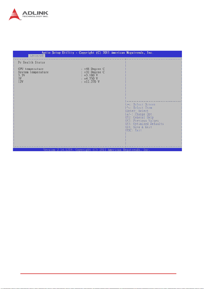
8.3.10 Hardware Monitor
This option displays the current status of all of the monitored hardware devices/components such as voltages and temperatures.
CPU Temperature
Displays current CPU temperature.
System Temperature
Displays current system temperature.
3.3V
Displays current system 3.3V voltage.
5V
Displays current system 5V voltage.
12V
Displays current system 12V voltage.
84 BIOS Setup
Page 97

cPCI-6520
8.3.11 Serial Port Console Redirection
You can use this screen to select options for the serial port console redirection settings. Use the up and down < Arrow > keys to
select an item. Use the < + > and < - > keys to change the value of
the selected option. A description of the selected item appears on
the right side of the screen. The settings are described on the following pages. An example of the Serial Port Console Redirection
screen is shown below.
Console Redirection
Set this value to Enabled/Disabled.
COM1/2/3 Console Redirection Settings
The settings specify how the host computer and the remote computer will exchange data. Both computers should have the same
or compatible settings. The screen is shown below.
BIOS Setup 85
Page 98

Terminal Type
VT100+ is the preferred terminal type for out-of-band management. Configuration options: VT100, VT100+, VT-UTF8, ANSI.
Bits per second
Select the bits per second you want the serial port to use for
console redirection. The options are 115200, 57600, 38400,
19200, 9600.
Data Bits
Select the data bits you want the serial port to use for console
redirection. Set this value to 7, 8.
Parity
Set this option to select Parity for console redirection. The settings for this value are None, Even, Odd, Mark, Space.
Stop B its
Stop bits indicate the end of a serial data packet. (A start bit
indicates the beginning). The standard setting is 1 stop bit.
Communication with slow devices may require more than 1
stop bit. Set this value to 1 and 2.
86 BIOS Setup
Page 99

cPCI-6520
Flow Control
Set this option to select Flow Control for console redirection.
The settings for this value are None, Hardware RTS/CTS.
VT-UTF8 Combo Key Support
Enables VT-UTF8 combination key support for ANSI/VT100
terminals.Set this value to Enabled/Disabled.
Recorder Mode
When this mode is enabled, only text will be sent. This is to
capture terminal data. Set this value to Enabled/Disabled.
Resolution 100x31
Set this option to extended terminal resolution. Set this val ue to
Enabled/Disabled.
Legacy OS Redirection
On legacy OS, the number of rows and columns supported for
redirection. Set this value to 80x24, 80x25.
Putty Key Pad
Select FunctionKey and KeyPad on Putty. Set this value to
VT100, LINUX, XTERMR6, SCO, ESCN, VT400.
Serial Port for Out-of-Band Management/Windows Emergency Management Services (EMS)
The following functions control the presence and content of the
ACPI serial port redirection table (SPCR). This table is mainly
used by the Windows server variants to prov ide Windows Emergency Management Services (EMS). This functionality is totally
independent from serial redirect ion of other console output. OoB
Management or EMS makes it possible to control selected components of (Windows) servers, even when a server is not connected
to the network or the network is not available. In short: EMS allows
for remote management of a Windows Server OS through a serial
port
BIOS Setup 87
Page 100

Out-of-Band Mgmt Port
Microsoft Windows emergency management services (EMS)
allows for remote management of a Windows Server OS
through a serial port. Set this value to COM0, COM1, COM2
(Disabled), COM3 (Disabled)
Terminal Type
VT-UTF8 is the preferred terminal type for out-of-band management. The next best choice is VT100+ and then VT100.
See above, in Console Redirection Settings page, for more
Help with Terminal Type/Emulation. Configuration options:
VT100, VT100+, VT-UTF8, ASNI.
Bits per second
Select the bits per second you want the serial port to use for
console redirection. The options are 115200 ,57600 ,38400,
19200, 9600.
Flow Control
Set this option to select Flow Control for console redirection.
The settings for this value are None and Hardware RTS/CTS.
Data Bits
This is a display-only function providing infor mation about the
frame width for the Out-of-Band Management.
88 BIOS Setup
 Loading...