

Page 1
cPCI-6510 Series
Low Power 6U CompactPCI Processor Blade
with Intel® Core™ i7 and two PMC sites
User’s Manual
Manual Rev. 2.02
Revision Date: November 13, 2014
Part No: 50-15071-1020
Advance Technologies; Automate the World.
Page 2

Revision History
Revision Release Date Description of Change(s)
2.00 2010/09/24 Initial Release
Updated RTM list, Mode Switch (SW2) definition,
2.01 2010/11/24
2.02 2014/11/13 Add PMC slot -12V support note
IPMI User Guide; added NT Mode EEPROM
programming instructions
Page 3

cPCI-6510
Preface
Copyright 2010-14 ADLINK Technology Inc.
This document contains proprietary information protected by copyright. All rights are reserved. No part of this manual may be reproduced by any mechanical, electronic, or other means in any form
without prior written permission of the manufacturer.
Disclaimer
The information in this document is subject to change without prior
notice in order to improve reliability, design, and function and does
not represent a commitment on the part of the manufacturer.
In no event will the manufacturer be liable for direct, indirect, special, incidental, or consequential damages arising out of the use or
inability to use the product or documentation, even if advised of
the possibility of such damages.
Environmental Responsibility
ADLINK is committed to fulfill its social responsibility to global
environmental preservation through compliance with the European Union's Restriction of Hazardous Substances (RoHS) directive and Waste Electrical and Electronic Equipment (WEEE)
directive. Environmental protection is a top priority for ADLINK.
We have enforced measures to ensure that our products, manufacturing processes, components, and raw materials have as little
impact on the environment as possible. When products are at their
end of life, our customers are encouraged to dispose of them in
accordance with the product disposal and/or recovery programs
prescribed by their nation or company.
Trademarks
Product names mentioned herein are used for identification purposes only and may be trademarks and/or registered trademarks
of their respective companies.
Preface iii
Page 4

Using this Manual
Audience and Scope
The cPCI-6510 User’s Manual is intended for hardware
technicians and systems operators with knowledge of installing,
configuring and operating industrial grade CompactPCI modules.
Manual Organization
This manual is organized as follows:
Chapter 1, Overview: Introduces the cPCI-6510, its features,
block diagrams, and package contents.
Chapter 2, Specifications: Presents detailed specification
information, and power consumption.
Chapter 3, Functional Description: Describes the cPCI-6510’s
main functions.
Chapter 4, Board Interfaces: Describes the cPCI-6510 board
interfaces, pin definitions, and jumper settings.
Chapter 5, Getting Sta rted: Describes the installation instructions
of the cPCI-6510.
Chapter 6, Driver Installation: Describes the driver installation
procedures.
Chapter 7, Utilities: Describes the Watchdog Timer and Preboot
Execution Environment functions.
Chapter 8, BIOS Setup Utility: Describes the AMIBIOS®8 BIOS
setup utility.
Chapter 9, IPMI User Guide: Provides relevant information for
the baseboard management controller (BMC) of the Intelligent
Platform Management Interface (IPMI).
Important Safety Instructions: Presents safety instructions all
users must follow for the proper setup, installation and usage of
equipment and/or software.
Getting Service: Contact information for ADLINK’s worldwide
offices.
iv Preface
Page 5
cPCI-6510
Conventions
Take note of the following conventions used throughout this
manual to make sure that users perform certain tasks and
instructions properly.
Additional information, aids, and tips that help users perform
tasks.
NOTE:
NOTE:
Information to prevent minor physical injury, component dam-
age, data loss, and/or program corruption when trying to com-
CAUTION:
WARNING:
plete a task.
Information to prevent serious physical injury, component
damage, data loss, and/or program corruption when trying to
complete a specific task.
Preface v
Page 6

This page intentionally left blank.
vi Preface
Page 7

cPCI-6510
Table of Contents
Revision History...................................................................... ii
Preface.................................................................................... iii
List of Tables.......................................................................... xi
List of Figures...................................................................... xiii
1 Overview ............................................................................. 1
1.1 Introduction .......................................................................... 1
1.2 Features............................................................................... 2
1.3 Block Diagram ..................................................................... 3
1.4 Product List.......................................................................... 4
1.5 Package Contents ............................................................... 5
2 Specifications..................................................................... 7
2.1 cPCI-6510 Specifications..................................................... 7
2.2 I/O Connectivity ................................................................. 10
2.3 Power Requirements ......................................................... 11
2.4 Thermal Requirements ...................................................... 13
3 Functional Description .................................................... 17
3.1 Processor........................................................................... 17
3.2 Chipset............................................................................... 18
3.3 Super I/O ........................................................................... 19
3.4 Battery ............................................................................... 19
3.5 PMC/XMC Sites................................................................. 19
3.6 BIOS Recovery .................................................................. 20
4 Board Interfaces............................................................... 21
4.1 cPCI-6510 Series Board Layout - Top Side....................... 21
4.2 cPCI-6510 Series Board Layout - Bottom Side ................. 22
Table of Contents vii
Page 8

4.3 cPCI-6510 SBC Front Panel .............................................. 23
4.4 Connector Pin Assignments............................................... 24
4.5 Switch and Jumper Settings .............................................. 38
5 Getting Started.................................................................. 41
5.1 Hard Drive Installation........................................................ 42
5.2 CompactFlash Card Installation......................................... 45
5.3 PMC/XMC Module Installation ........................................... 46
5.4 Installing the cPCI-6510 to the Chassis ............................. 47
5.5 Installing the RTM to the Chassis ...................................... 48
6 Driver Installation.............................................................. 49
6.1 Driver Installation Procedure.............................................. 49
7 Utilities............................................................................... 51
7.1 Watchdog Timer................................................................. 51
7.2 Preboot Execution Environment (PXE).............................. 56
7.3 BIOS Recovery .................................................................. 57
7.4 Programming NT Mode EEPROM Map ............................. 59
8 BIOS Setup Utility............................................................. 61
8.1 Starting the BIOS ............................................................... 61
8.2 Main Setup......................................................................... 64
8.3 Advanced BIOS Setup ....................................................... 65
8.4 Chipset Configuration ........................................................ 75
8.5 Boot Configuration ............................................................. 78
8.6 Security Setup.................................................................... 80
8.7 Save & Exit ........................................................................ 81
9 IPMI User Guide ................................................................ 83
9.1 Introduction ........................................................................ 83
9.2 Summary of Commands Supported by BMR-AVR-cPCI ... 83
9.3 OEM Commands Summary Table ..................................... 87
9.4 CompactPCI Address Map ................................................ 91
viii Table of Contents
Page 9

cPCI-6510
9.5 Communications with IPMC............................................... 92
9.6 IPMI Sensors List............................................................... 92
9.7 Relevant Documents ......................................................... 92
Important Safety Instructions.............................................. 93
Getting Service...................................................................... 95
Table of Contents ix
Page 10

This page intentionally left blank.
xTable of Contents
Page 11

cPCI-6510
List of Tables
Table 2-1: cPCI-6510 Specifications ......................................... 8
Table 2-2: cPCI-6510 I/O Connectivity .................................... 10
Table 2-3: CompactPCI Input Voltage Characteristics ............ 11
Table 2-4: Idle Mode Power Consumption .............................. 12
Table 2-5: 100% CPU Usage Power Consumption ................. 12
Table 4-1: cPCI-6510 Front Panel Status LED Descriptions ... 23
Table 4-2: USB Connector Pin Definition ................................ 24
Table 4-3: RJ-45 Serial Port Pin Definition .............................. 24
Table 4-4: GbE Connector Pin Definitions ............................... 25
Table 4-5: DVI-I Connector Pin Definition ................................ 26
Table 4-6: DB-6920SAT SATA Connector Pin Definition ........ 27
Table 4-7: PMC Connector Pin Definitions .............................. 28
Table 4-8: XMC Connector Pin Definition ................................ 30
Table 4-9: CompactFlash Connector Pin Definition ................. 31
Table 4-10: DB-6920SAT Connector Pin Definition ................... 32
Table 4-11: CompactPCI J1 Connector Pin Definition ............... 33
Table 4-12: CompactPCI J2 Connector Pin Definition ............... 34
Table 4-13: CompactPCI J3 Connector Pin Definition ............... 35
Table 4-14: CompactPCI J4 Connector Pin Definition ............... 36
Table 4-15: CompactPCI J5 Connector Pin Definition ............... 37
Table 4-16: Mode Switch Settings ............................................. 39
Table 4-17: PMC Bandwidth/Clock Switch Settings .................. 39
Table 4-18: COM1/Debug Switch Settings ................................ 40
Table 4-19: Front/Rear VGA Selection Switch Settings ............ 40
List of Tables xi
Page 12

This page intentionally left blank.
xii List of Tables
Page 13

cPCI-6510
List of Figures
Figure 1-1: cPCI-6510 Series Block Diagram .............................. 3
Figure 2-1: Core i7-610E Power Dissipation Graph (TDP 35W) 14
Figure 2-2: Core i7-620LE Power Dissipation Graph (TDP 25W) 14
Figure 2-3: Core i7-620UE Power Dissipation Graph (TDP 18W) 15
Figure 4-1: cPCI-6510 Series Board Layout - Top Side ............ 21
Figure 4-2: cPCI-6510 Series Board Layout - Bottom Side ....... 22
Figure 4-3: cPCI-6510 Series Front Panel Layout ..................... 23
List of Figures xiii
Page 14

This page intentionally left blank.
xiv List of Figures
Page 15

1Overview
1.1 Introduction
The cPCI-6510 Series is a 6U CompactPCI single board computer
in single slot width (4HP) form factor supporting 32nm Intel®
Core™ i7 SV, LV, ULV processors with integrated graphics and
ECC memory controller onboard. The cPCI-6510 provides up to
8GB of dual channel DDR3-800/1066 ECC memory soldered
onboard and implements the Mobile Intel® QM57 Express Chipset
to provide a full feature set and optimal performance per watt.
The cPCI-6510 Series provides a 64bit/66MHz CompactPCI bus,
up to two PMC sites with 64-bit/133MHz PCI-X bus supporting
rear I/O (PIM), and one PCI Express x8 XMC site (shared with
inner PMC site). Featured I/O includes four PCI Express Gigabit
Ethernet ports (two on front panel, two for PICMG 2.16), two USB
ports and a CompactFlash socket. DVI-I, COM and additional USB
ports are available on the cPCI-6510V version which also provides
a SATA connector for an onboard 2.5” SATA HDD. Optional Rear
Transition Modules provide versatile additional I/O including two
additional GbE, USB, COM, High Definition Audio, and storage
interfaces such as SATA, SCSI, and SAS with RAID support. The
cPCI-6510V supports dual independent display via two DVI or one
DVI and one VGA when accompanied by the appropriate Rear
Transition Module.
For flexibility of use, the cPCI-6510 Series can be installed in a
standard CompactPCI system slot as system master, or peripheral
slot as a PCI device. Through hardware switch setting, the
cPCI-6510 optionally supports operation in system or peripheral
slots as a standalone blade. The cPCI-6510 Series is ideally
suited for military, aviation, communication and other industrial
applications.
cPCI-6510
Overview 1
Page 16

1.2 Features
X 6U CompactPCI SBC in 4HP width form factor
X µFC-BGA package Intel® Core™ i7 processor, up to 2.53GHz
X Mobile Intel® BD82QM57 PCH (Platform Controller Hub)
X Dual Channel DDR3 ECC SDRAM at 800 or 1066MHz sol-
dered onboard, up to 8GB
X 64-bit/66MHz CompactPCI Interface based on PCI specifica-
tions, 3.3V and 5V signaling
X Supports operation in system slot as system master or in
peripheral slot with connectivity to CompactPCI bus* (optional
isolation from CompactPCI bus)
X Dual PMC sites with 64-bit/133MHz PCI bus
X Single XMC site with PCIe x8 lane (shared with inner PMC
site)
X Up to two DVI ports for dual independent displays
X Four PCIe Gigabit Ethernet ports, two at front, two for PICMG
2.16 or RTM
X Onboard CompactFlash socket
X 2.5” SATA HDD direct connector onboard, occupies outer PMC
site
X Up to -40°C to 80°C optional extended temperature support
X RTM models available with multiple I/O options: SATA, HD
audio, COM, USB, Gigabit Ethernet, PS/2 KB/MS, PIM, SAS,
SCSI, CF, SD socket
X Hardware RAID on SCSI, SAS interfaces supported (depen-
dent on RTM module)
*See “Programming NT Mode EEPROM Map” on page 59 for
instructions on how to set the PCIe-to-PCI bridge on the
NOTE:
NOTE:
cPCI-6510 to NT-mode to allow operation in a peripheral slot.
2Overview
Page 17
1.3 Block Diagram
Front Panel
3x USB
COM1
GbE1 GbE2
cPCI-6510
DVI-I
Soldered w/ ECC, max. 4GB
Soldered w/ ECC, max. 4GB
DDR3 800/1066
PCIe x8
Rear I/O
DMI
SATA1
COM4
IPMB 0/1
ITE8783
BMC
SIO
LPC
KB/MS
2x COM
Pericom
PI7C9X13
PCI 64b/66M
Intel® Core™ i7
PCIe x8
PCIe
Switch
PCIe x4
PCIe x4
Pericom
PI7C9X13
PCI-X 64b/133M
PMC 2
Rear I/O
2.5” HDD
XMC
PMC 1
J1/J2 J3/J4/J5
Figure 1-1: cPCI-6510 Series Block Diagram
Intel
82574L
Intel
82574L
PCIe x1 PCIe x1 TMDSA
QM57 PCH
PCIe x1 PCIe x1
Intel
82574L
GbE4
Intel
82574L
GbE3
6x USB
3x SATA
HDA
5x GPIO
RTC
PCIe x4
LVD S
RGB
SW
SATA2
SPI
TMDSB
SATA
to IDE
BIOS
CF
RGB
Overview 3
Page 18

1.4 Product List
Products included in the cPCI-6510 Series include:
Processor Blade
X cPCI-6510: 4HP width (single-slot) 6U CompactPCI blade
featuring single Intel® Core™i7 processor, dual channel
DDR3-800/1066 soldered onboard SDRAM with ECC,
2x PMC or 1x PMC and 1x XMC, 2x USB, 2x GbE and CF
socket
X cPCI-6510V: 4HP width (single-slot) 6U CompactPCI blade
featuring single Intel® Core™i7 processor, dual channel
DDR3-800/1066 soldered onboard SDRAM with ECC,
1x PMC/XMC, 3x USB, 2x GbE, RJ-45 COM, DVI-I, SATA
for 2.5” HDD and CF socket
Rear Transition Modules
X cPCI-R6000: 4HP width RTM with DVI-I, 2x COM, 3x USB, 2x
GbE, SCSI, 2xSATA
X cPCI-R6100: 4HP width RTM with 4x GbE, 4x USB, 2xSATA,
DVI, VGA, PS/2 KB/MS, CF & SD sockets
X cPCI-R6110: 4HP width RTM with 2x GbE, 4x USB, 3x SATA,
VGA, PS/2 KB/MS, CF, & SD sockets
X cPCI-R6200: 8HP width RTM with 2x GbE, 2x COM, 4x USB,
DVI-I, 3x SATA, Mic-in, Line-out, PS/2 KB/MS, 8x SAS
X cPCI-R6210: 4HP width RTM with 2xUSB, DVI-I, COM,
2x SATA, 2x PIM
Adapter Kit
X DB-CF-SA: CompactFlash socket kit for cPCI-R6000D &
cPCI-R6200 RTMs, including DB-6920CF adapter board, card
guide and screws to replace SATA adapter with CompactFlash
socket
4Overview
Page 19

cPCI-6510
1.5 Package Contents
The cPCI-6510 is packaged with the components listed below
(RTMs and adapter kits are optional). If any of the items in the
contents list are missing or damaged, retain the shipping carton
and packing material and contact the dealer for inspection. Please
obtain authorization before returning any product to ADLINK. The
packing contents of non-standard configurations may vary
depending on customer requests.
Processor Blade
X The cPCI-6510 Series Processor Blade
Z CPU, RAM will differ depending on options selected
Z Thermal module is assembled on the board
X RJ-45 to DB-9 cable for RJ-45 COM port (cPCI-6510V only)
X 2.5” SATA HDD mounting kit, including HDD bracket,
screws for HDD, and DB-6920SAT SATA adapter card
(cPCI-6510V only)
X ADLINK All-in-One CD
X User’s manual
The contents of non-standard cPCI-6510 configurations may
vary depending on customer requests.
NOTE:
NOTE:
This product must be protected from static discharge and physical shock. Never remove any of the components except at a
CAUTION:
static-free workstation. Use the anti-static bag shipped with the
product when putting the board on a surface. Wear an
anti-static wrist strap properly grounded on one of the system's
ESD ground jacks when installing or servicing system components.
Overview 5
Page 20

This page intentionally left blank.
6Overview
Page 21

2 Specifications
2.1 cPCI-6510 Specifications
PICMG® 2.0 CompactPCI® Rev. 3.0
CompactPCI
Standard
Mechanical
Processor
Chipset Intel® QM57 Platform Controller Hub (PCH)
Memory
CompactPCI Bus
PMC/XMC
Graphics
Ethernet
PICMG® 2.1 Hot Swap Specification Rev.2.0
PICMG® 2.9 System Management Bus Rev. 1.0
PICMG® 2.16 Packet Switching Backplane Rev.1.0
Standard 6U CompactPCI®
Board size: 233.23 mm x 160mm
Single slot (4HP, 20.32mm) width
CompactPCI® connectors J1, J2, J3, J4 and J5
µFC-BGA Intel® Core™i7-610E, 4MB L2 cache, 2.53GHz
µFC-BGA Intel® Core™i7-620LE, 4MB L2 cache, 2.0GHz
µFC-BGA Intel® Core™i7-620UE, 4MB L2 cache, 1.06GHz
Dual channel DDR3-800/1066 soldered onboard SDRAM
with un-buffered ECC
DDR3-800 for Core™i7-620UE processor
DDR3-1067 for Core™i7-610E/620LE processors
Maximum 8GB capacity
PCI 64-bit/ 66MHz; V(I/O) 3.3V and 5V signaling
Supports operation in system slot or in peripheral slot with
connectivity to CompactPCI bus (Universal Mode)
Optional Satellite mode by switch setting
Two PCI 64-bit/133MHz PMC sites, V(I/O) 3.3V (contact
ADLINK for 5V support)
One PCIe x8 XMC site (shared with inner PMC site)
Integrated in Intel® Core™i7 processor
One DVI-I port on front panel of cPCI-6510V provides digital
and analog signals.
Analog RGB signal to front or rear by switch selection
Second DVI port routed to rear
Supports dual independent display
Analog RGB up to QXGA
Four PCIe x1 Intel® 82574L GbE controllers
Two 10/100/1000BASE-T egress ports
Two 10/100/1000BASE-T ports on rear panel, optional
PICMG 2.16 support by switch selection
cPCI-6510
1
Specifications 7
Page 22

One 16C550 compatible RJ-45 RS-232 port on front panel
Serial Ports
(cPCI-6510V only)
Two serial ports routed to rear I/O
Storage
Interfaces
2.5” SATA HDD direct connector onboard (cPCI-6510V only)
CompactFlash Type II socket onboard
1
BIOS AMI® EFI BIOS 64Mbit SPI flash memory
Supports PICMG® 2.9 secondary system management bus
IPMI functions implemented as defined by IPMI Spec. v1.5;
IPMI Interface
ATmega128L-8AU Baseboard Management Controller
(BMC) with 128KB programmable in-system flash, 4KB
EEPROM, and 4KB internal SDRAM
cPCI-6510:
2x USB 2.0 ports
2x 10/100/1000BASE-T Ethernet ports
2x PMC and one XMC slots
Faceplate I/O
cPCI-6510V:
3x USB 2.0 ports
2x 10/100/1000BASE-T Ethernet ports
PMC/XMC slot
RJ-45 Serial port
DVI-I port (digital and analog)
Microsoft® Windows® 7 Ultimate
Microsoft® Windows® Vista Enterprise
Supported OS
Microsoft® Windows® XP Professional SP3
Fedora™ 12
Other OS support upon request
Operating
Temperature
Storage
temperature
0°C to 60°C standard
-20°C to +70°C (cPCI-ET6510)
2
-40°C to +80°C (cPCI-EX6510)
-40°C to 85°C
Humidity 20% to 95% non-condensing
Shock 20G peak-to-peak, 11ms duration, non-operating
Vibration
3
Operating: 1.88Grms. 5 to 500Hz, each axis (without HDD)
Compliance CE EN55022, FCC Class A
T able 2-1: cPCI-6510 Specifications
8 Specifications
Page 23

Notes:
1. 7.4 "Programming NT Mode EEPROM Map" on page 59 for
instructions on how to set the PCIe-to-PCI bridge on the
cPCI-6510 to Non-Transparent mode to allow operation in a
peripheral slot.
2. ADLINK-certified thermal design. The thermal performance is
dependent on the chassis cooling design. Sufficient forced airflow is required (see 2.4 "Thermal Requirements" on page 13).
Temperature limit of optional mass storage devices may affect
the thermal specification.
3. The hard drive limits the operational vibration tolerance. When
application requires higher specification for anti-vibration, it is
recommended to use a solid state drive (SSD) or CompactFlash card.
Specifications are subject to change without prior notice.
NOTE:
NOTE:
cPCI-6510
Specifications 9
Page 24

2.2 I/O Connectivity
cPCI-6510 Processor Blade
Function
GbE 2—2—
USB 2.0 2—2—
COM ——1
DVI-I —— 1
PMC —2—1
XMC —1—1
Serial ATA — — — 1 (2.5” HDD)
CompactFlash —1—1
Table 2-2: cPCI-6510 I/O Connectivity
cPCI-6510 cPCI-6510V
Faceplate Board Faceplate Board
(RJ-45) —
10 Specifications
Page 25

cPCI-6510
2.3 Power Requirements
In order to guarantee a stable functionality of the system, it is rec-
ommended to provide more power than the system requires. An
industrial power supply unit should be able to provide at least
twice as much power as the entire system requires of each
voltage. An ATX power supply unit should be able to provide at
least three times as much power as the entire system requires.
The tolerance of the voltage lines described in the CompactPCI
specification (PICMG 2.0 R3.0) is +5%/ -3% for 5, 3.3 V and ±5%
for ±12V. This specification is for power delivered to each slot and
it includes both the power supply and the backplane tolerance.
Voltage
5V +5.0 VDC +5% / -3% 50 mV
3.3V +3.3 VDC +5% / -3% 50 mV
+12V +12 VDC +5% / -5% 240 mV
-12V -12 VDC +5% / -5% 240 mV
V I/O (PCI I/O
Buffer Voltage)
GND
Table 2-3: Comp actPCI Input Voltage Characteristics
Nominal
Value
+3.3 VDC or
+5 VDC
Tolerance
+5% / -3% 50 mV
Max. Ripple
(P - P)
Specifications 11
Page 26
Power Consumption
This section provides information on the power consumption of the
cPCI-6510 Series with different CPUs, 2GB DDR3-800/1066 soldered memory, and 100GB SATA HDD. The system was tested in
Idle Mode and Full Load Mode under Windows XP running Burn-in
Test 6.0. The cPCI-6510 is powered by 5V and 3.3V.
Idle Mode under Windows XP
CPU Core™ i7 610E Core™ i7 620LE Core™ i7 620UE
Voltage
+3.3 4.19 13.82 4.12 18.41 3.85 12.71
Total 19.51 23.76 17.96
100% CPU Usage under Windows XP
CPU Core™ i7 610E Core™ i7 620LE Core™ i7 620UE
Voltage
+3.3 6.09 20.10 5.83 19.25 5.31 17.52
Total 42.31 37.08 27.87
Current
(V)
+5 1.14 5.69 1.07 5.35 1.05 5.25
(V)
+5 4.44 22.21 3.57 17.83 2.07 10.35
(A)
Table 2-4: Idle Mode Power Consumption
Current
(A)
Power
(W)
Power
(W)
Current
(A)
Current
(A)
Power
(W)
Power
(W)
Current
(A)
Current
(A)
Power
(W)
Power
(W)
T able 2-5: 100% CPU Usage Power Consumption
12 Specifications
Page 27

cPCI-6510
2.4 Thermal Requirements
This section provides information on the thermal requirements of
the cPCI-6510 Series. Cooling of the board and its components is
provided by the thermal module (passive heatsink) and is dependent on sufficient airflow from the chassis.
The amount of thermal energy that can by dissipated from the
board is dependent on the ambient air temperature and the airflow
rate of the chassis. To provide the user with guidelines for the
upper limits of operating conditions for the cPCI-6510, the following sections give information on the maximum ambient air temperature as a function of airflow rate for a given level of power
consumption.
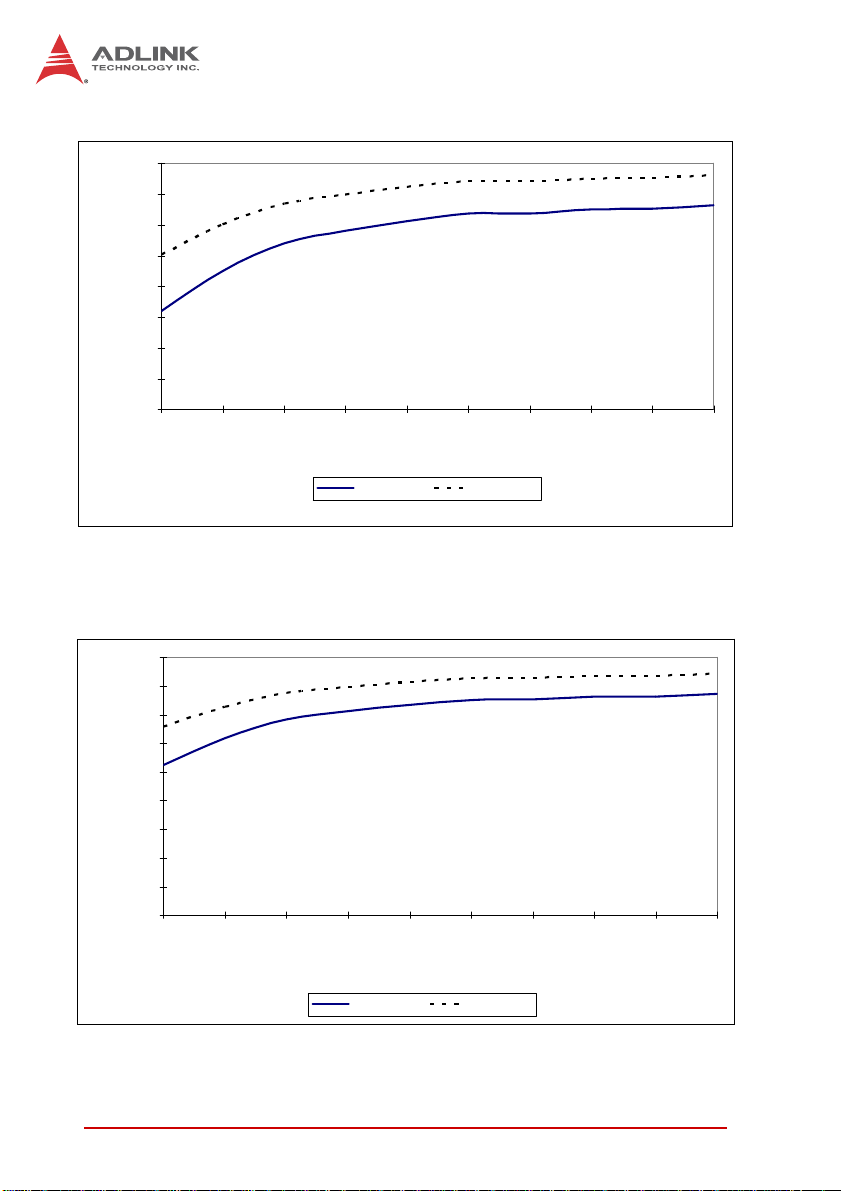
Power Dissipation Graphs
The graphs shown below illustrate the level of CPU power dissipation that can be maintained dependent on ambient air temperature
and airflow rate. One graph is provided for each CPU supported
by the cPCI-6510. The curves on each graph indicate the upper
limits of operating conditions under which the CPU will not be
affected by its thermal management and protection systems at a
given percentage of the CPU’s thermal design power (TDP).
The CPU’s thermal management and protection systems begin to
take effect when the CPU temperature exceeds the maximum
junction temperature (T
perature and airflow rate are in the ranges below the TDP curves
on the graphs, the CPU temperature will remain below T
the CPU will be able to operate at full performance (i.e. not limited
by thermal management).
The power dissipation graphs show two curves:
=105°C). When the ambient air tem-
j,Max
j,Max
and
X 100% TDP
X 75% TDP
The detailed specifications for each processor can be found in
Section 3.1 "Processor" on page 17.
Specifications 13
Page 28
Intel® Core™ i7-610E
80
70
60
50
40
30
20
Max. Air Inlet Temp. (°C)
10
0
4 6 9 12151821242730
Airflow Rate (CFM)
100% TDP 75% TDP
Figure 2-1: Core i7-610E Power Dissipation Graph (TDP 35W)
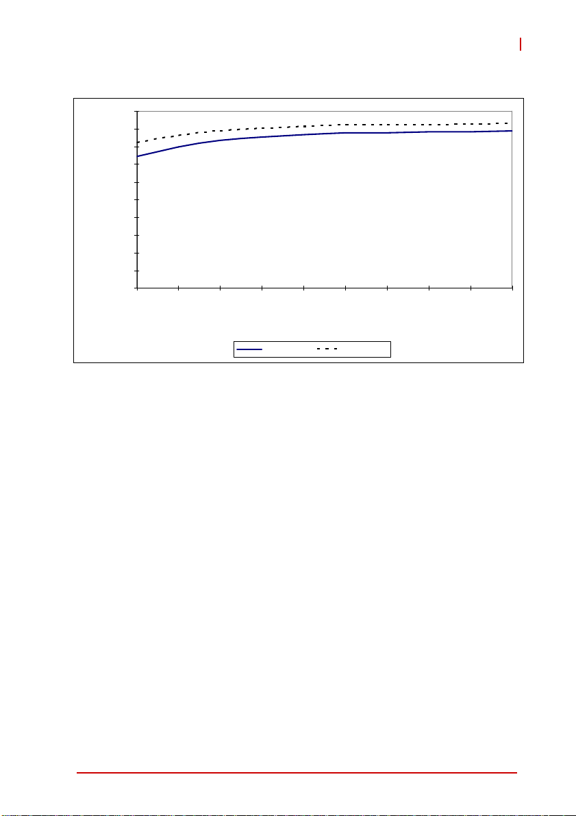
Intel® Core™ i7-620LE
90.0
80.0
70.0
60.0
50.0
40.0
30.0
20.0
Max. Air Inlet Temp. (°C)
10.0
0.0
4 6 9 12151821242730
Airflow Rate (CFM)
100% TDP 75% TDP
Figure 2-2: Core i7-620LE Power Dissipation Graph (TDP 25W)
14 Specifications
Page 29
Intel® Core™ i7-620UE
100.0
90.0
80.0
70.0
60.0
50.0
40.0
30.0
20.0
Max. Air Inlet Temp. (°C)
10.0
0.0
4 6 9 12 15 18 21 24 27 30
Airflow Rate (CFM)
100% TDP 75% TDP
Figure 2-3: Core i7-620UE Power Diss ipation Graph (TDP 18W)
cPCI-6510
Specifications 15
Page 30

Thermal Management Features
When the CPU temperature exceeds its maximum junction temperature (T
reduce power consumption (and thus performance) in an attempt
to reduce the core junction temperature. Use of the CPU’s thermal
management features is intended for short periods of time when
running power intensive applications. If the system is operated
under conditions below the TDP curves above, activation of the
thermal management features will be minimal and reduction in
CPU performance will be minor.
However, if the operating conditions are outside the limits set out
above, the CPU temperature may exceed T
periods, resulting in noticeable performance loss and reduced reliability of the processor.
In extreme situations, the thermal management features may be
incapable of cooling the processor. If the CPU temperature
exceeds approximately 130°C, a catastrophic cooling failure will
be detected and the processor will automatically shut down to prevent physical damage to the processor.
WARNING:
), the CPU’s thermal management features will
j,Max
for prolonged
j,Max
Prolonged operation above the CPU’s maximum junction temperature (Tj,Max=105°C) may damage the CPU and/or reduce
its long term reliability. Be sure to follow the thermal guidelines
set out in this document.
16 Specifications
Page 31

cPCI-6510
3 Functional Description
The following sections describe the cPCI-6510 Series features
and functions.
3.1 Processor
Intel® Core™ i7 Processor
The Intel® Core™ i7-620LE/UE and i7-610E are 64-bit, multi-core
mobile processors built on a 32 nanometer process technology.
The processors are designed for a two-chip platform consisting of
a processor and the Platform Controller Hub (PCH) and enables
higher performance, lower cost, easier validation, and improved
x-y footprint. The Intel® Core™ i7-620LE/UE and i7-610E processors are offered in a BGA1288 package and include an integrated
graphics and memory controller die on the same package as the
processor core die.
The following table lists the processors supported by the
cPCI-6510 Series and their specifications.
Features SV Core i7-610E LV Core i7-620LE ULV Core i7-620UE
Clock 2.53GHz 2.0GHz 1.06GHz
Max. Turbo Freq. 3.2GHz 2.8GHz 2.13GHz
L2 cache 4MB 4MB 4MB
Max. Power (TDP1)
2
T
j,Max
Process 32nm 32nm 32nm
# of cores/threads 2/4 2/4 2/4
35W 25W 18W
105°C 105°C 105°C
Notes:
1. The highest expected sustainable power while running known
power intensive applications. TDP is not the maximum power
that the processor can dissipate.
2. Maximum junction temperature (T
ported operating temperature.
Functional Description 17
). The maximum sup-
j,Max
Page 32

System Memory Support
X Two channels of DDR3 memory soldered onboard
X Memory DDR3 data transfer rates of 800 and 1066 MT/s
X 64-bit wide channels (72-bit wide including ECC)
X Supports ECC unbuffered DDR3 memory
X Theoretical maximum memory bandwidth of:
Z
12.8 GB/s in dual-channel mode assuming DDR3 800 MT/s
Z
17.1 GB/s in dual-channel mode assuming DDR3 1066 MT/s
X 1-Gb and 2-Gb DDR3 DRAM technologies for x8 devices
X Using 2Gb device technologies, the largest memory capac-
ity is 8GB
3.2 Chipset
Mobile Intel® QM57 Express Chipset
The cPCI-6510 Series incorporates the Mobile Intel® QM57
Express Chipset, also referred to as PCH (Platform Controller
Hub), to provide extensive I/O support. Functions and capabilities
include:
X PCI Express Base 2.0 Specification support for up to eight
ports
X 4 PCI Express x1 connected to LAN controllers
X 4 PCI Express x1 are configured to PCI Express x4 and
routed to J5 for I/O expansion
X ACPI Power Management Logic Support
X Two integrated SATA host controllers with up to six ports,
supporting independent DMA operation and data transfer
rates of up to 3.0GB/s (the cPCI-6510 supports up to four
SATA ports)
X Supports Advanced Host Controller Interface (AHCI)
X Intel Rapid Storage Technology provides high performance
RAID 0, 1, 5, and 10 functionality
X High speed USB 2.0 allows data transfers up to 480 Mb/s
X Provides Intel Virtualization Technology with Directed I/O
(Intel VT-d) support.
18 Functional Description
Page 33

cPCI-6510
3.3 Super I/O
The ITE IT8783F Super I/O is on a Low Pin Count interface supporting PS/2 keyboard/mouse, 16C550-compatible serial ports,
floppy drive interface, hardware monitor function to monitor CPU
voltage, CPU temperature, power supply voltages and system temperature, and Watchdog Timer with time resolution from minimum 1
second or minute to maximum 65,535 seconds or minutes.
3.4 Battery
The cPCI-6510 is provided with a 3.0V coin cell lithium battery for
the Real Time Clock (RTC). The lithium battery must be replaced
with an identical battery or a battery type recommended by the
manufacturer. A Rayovac BR2032 is equipped on board by
default.
3.5 PMC/XMC Sites
The cPCI-6510 series supports two PMC sites for front panel I/O
expansion. The PMC sites provides a maximum 64bit/133MHz
PCI-X bus link using a Pericom PI7C9X130 PCIe-to-PCI bridge
and PCIe x4 link. The PMC/XMC sites support +3.3V signaling
and 5V VPWR by default. For optional 5V signaling and 12V
VPWR support, contact your ADLINK sales representative.
The JN1/5 and JN2/6 connectors provide the signals for the 32-bit
PCI bus. The JN3/7 connector provides the 64 bit extension for the
PMC interface. The JN3/7 connectors support user defined I/O
signals and are routed to the CompactPCI J4/5 connectors to rear
I/O.
The cPCI-6510 provides a PCIe x8 XMC interface sharing the
same space as the inner PMC site for high speed I/O expansion,
such as 10GbE or high-end graphics.
Functional Description 19
Page 34

3.6 BIOS Recovery
The cPCI-6510 Series features AMI® EFI BIOS with BIOS recovery. If the BIOS becomes corrupted and you are unable to boot
your system, follow the instructions in Section 7.3 “BIOS Recovery” on page 57.
20 Functional Description
Page 35

4 Board Interfaces
This chapter describes the board layout, connector pin assignments, and jumper settings of the cPCI-6510 Series.
4.1 cPCI-6510 Series Board Layout - Top Side
The cPCI-6510 and cPCI-6510V have the same PCB layout but
different BOM options to offer different features.
cPCI-6510
cPCI-6510
U3
SDRAM
U40
CN5
SW1
SW2
CN8
SW3
J5
JN5 JN7
JN6 JN8
J4
JN1 JN3
JN2 JN4
J3
J2
J1
cPCI-6510V
CN3
U3
SDRAM
U40
CN5
CN8
SW3
SW1
SW2
JN1 JN3
U40 CPU CN3 DB-6920SAT connector
U3 QM57 PCH CN5 CompactFlash socket
SDRAM Soldered SDRAM CN8 XMC connector
J1-5 CompactPCI connectors JN1-8 PMC connectors
SW1-3 Switches
J5
J4
JN2 JN4
J3
J2
J1
Figure 4-1: cPCI-6510 Series Board Layout - Top Side
Board Interfaces 21
Page 36

4.2 cPCI-6510 Series Board Layout - Bottom Side
SW6
SDRAM
SW4
SW5
SW8
SW4/5/6/8 Switches SDRAM Soldered SDRAM
Figure 4-2: cPCI-6510 Series Board Layout - Bottom Side
22 Board Interfaces
Page 37

4.3 cPCI-6510 SBC Front Panel
cPCI-6510V
cPCI-6510
cPCI-6510
Status LEDs
Power (P) Green
Hot Swap
PMC
DVI-I
PMC/XMC GbE 1/2
2x USB
Status LEDs
COM1 USB
Figure 4-3: cPCI-6510 Series Front Panel Layout
HPWDRST
LED Color Condition Indication
OFF System is off
ON System is on
OFF Handles closed, System is on
Preparing to shut down system
(LED: 0.1s on, 0.9s off)
Handles open and SBC ready
to be removed
(H)
Blue
Fast Blink
ON
Voltages out of tolerance:
Slow Blink
3.3V, 5V, 12V, 1.5V over ±5%
(LED: 2s on, 1s off)
HDD
(D)
WDT
(W)
Red
Amber
OFF No HDD activity
Blink Data read/write in process
OFF No Watchdog event
ON Watchdog event alert
Table 4-1: cPCI-6510 Front Panel Status LED Descriptions
Board Interfaces 23
Page 38

4.4 Connector Pin Assignments
Refer to “cPCI-6510 Series Board Layout - Top Side” on page 21
and “cPCI-6510 Series Front Panel Layout” on page 23 for connector locations
USB Connectors
Pin # Signal Name
1Vcc
2UV0-
3UV0+
4GND
Table 4-2: USB Connector Pin Definition
RJ-45 COM1 Port
Pin # COM Signal
1DCD#
2RTS#
3DSR#
4TXD
5RXD
6GND
7CTS#
8DTR#
1
6
Table 4-3: RJ-45 Serial Port Pin Definition
24 Board Interfaces
Page 39

RJ-45 Gigabit Ethernet Connectors
cPCI-6510
Pin #
Network link is not established
10BASE-T/100BAS
E-TX
1 TX+ BI_DA+
2 TX- BI_DA-
3 RX+ BI_DB+
4 -- BI_DC+
5 -- BI_DC-
6 RX- BI_DB-
7 -- BI_DD+
8 -- BI_DD-
Table 4-4: GbE Connector Pin Definitions
Status (CN4, CN5)
or system powered off
10 Mbps
100 Mbps
1000 Mbps
Link OFF ON
Active OFF Blinking
Link Green ON
Active Green Blinking
Link Amber ON
Active Amber Blinking
1000BASE-T
Speed LED
(Green/Amber)
81
Speed Activity
Activity LED
(Amber)
OFF OFF
Board Interfaces 25
Page 40

DVI-I Connector
Pin # Signal Pin # Signal
1 TMDS Data2- 16 Hot Plug Detect
2 TMDS Data2+ 17 TMDS Data0-
3 GND 18 TMDSData0+
4NC19GND
5NC20NC
6 DDC Clock [SCL] 21 NC
7 DDC Data [SDA] 22 GND
8 Analog vertical sync 23 TMDS Clock +
9 TMDS Data1- 24 TMDS Clock -
10 TMDS Data1+ C1 Analog Red
11 GND C2 Analog Green
12 NC C3 Analog Blue
13 NC C4 Analog Horizontal Sync
14 +5 V Power C5 Analog GND Return
15 GND
Table 4-5: DVI-I Connector Pin Definition
26 Board Interfaces
Page 41

Serial ATA Connector on DB-6920SAT
Pin # Signal
S1 GND
S2 TX+
S3 TX-
S4 GND
S5 RX-
S6 RX+
S7 GND
P1 NC
P2 NC
P3 NC
P4 GND
P5 GND
P6 GND
P7 5V
P8 5V
P9 5V
P10 GND
P11 Reserved
P12 GND
P13~P15 12V
cPCI-6510
S1
Signal
S7
P1
Power
P15
Table 4-6: DB-6920SAT SATA Connector Pin Definition
Board Interfaces 27
Page 42

PMC Connector (JN1/5, JN2/6, JN3/7, JN4/8)
Pin# JN1/5 Signal JN2/6 Signal JN3/7 Signal JN4/8 Signal
1 PMC_TCK P12V NC PIO1
2 N12V* PMC_TRST-L GND PIO2
3 GND PMC_TMS GND PIO3
4 PCIX_INTA-L NC (PMC_TDO) PCIX_CBE-L7 PIO4
5 PCIX_INTB-L PMC_TDI PCIX_CBE-L6 PIO5
6 PCIX_INTC-L GND PCIX_CBE-L5 PIO6
7 PMC_MOD-L1 GND PCIX_CBE-L4 PIO7
8 P5V NC GND PIO8
9 PCIX_INTD-L NC PMC_VIO PIO9
10 NC NC PCIX_PAR64 PIO10
11 GND PMC_MOD-L2 PCIX_AD63 PIO11
12 P3V3_PMCAUX P3V3 PCIX_AD62 PIO12
13 CLK66_PCIX_PMC PMC_RST-L PCIX_AD61 PIO13
14 GND PMC_MOD-L3 GND PIO14
15 GND P3V3 GND PIO15
16 PCIX_GNT-L0 PMC_MOD-L4 PCIX_AD60 PIO16
17 PCIX_REQ-L0 PMC_PME-L PCIX_AD59 PIO17
18 P5V GND PCIX_AD58 PIO18
19 PMC_VIO PCIX_AD30 PCIX_AD57 PIO19
20 PCIX_AD31 PCIX_AD29 GND PIO20
21 PCIX_AD28 GND GND PIO21
22 PCIX_AD27 PCIX_AD26 PCIX_AD56 PIO22
23 PCIX_AD25 PCIX_AD24 PCIX_AD55 PIO23
24 GND PCIX_AD23 PCIX_AD54 PIO24
25 GND PMC_IDSEL PCIX_AD53 PIO25
26 PCIX_CBE-L3 PCIX_AD23 GND PIO26
27 PCIX_AD22 P3V3 GND PIO27
28 PCIX_AD21 PCIX_AD20 PCIX_AD52 PIO28
29 PCIX_AD19 PCIX_AD18 PCIX_AD51 PIO29
30 P5V GND PCIX_AD50 PIO30
31 PCIX_FRAME-L PCIX_AD16 PCIX_AD49 PIO31
32 PCIX_AD17 PCIX_CBE-L2 GND PIO32
6364
12
Table 4-7: PMC Connector Pin Definitions
*Note: -12V signal not supported on JN1/5 pin 2. Contact ADLINK for
more information.
secafretnI draoB82
Page 43

cPCI-6510
Pin# JN1/5 Signal JN2/6 Signal JN3/7 Signal JN4/8 Signal
33 PCIX_FRAME-L GND GND PIO33
34 GND NC PCIX_AD48 PIO34
35 GND PCIX_TRDY-L PCIX_AD47 PIO35
36 PCIX_IRDY-L P3V3 PCIX_AD46 PIO36
37 PCIX_DEVSEL-L GND PCIX_AD45 PIO37
38 P5V PCIX_STOP-L GND PIO38
39 PCIX_PCIXCAP PCIX_PERR-L GND PIO39
40 PCIX_LOCK-L GND PCIX_AD44 PIO40
41 NC P3V3 PCIX_AD43 PIO41
42 NC PCIX_SERR-L PCIX_AD42 PIO42
43 PCIX_PAR PCIX_CBE-L1 PCIX_AD41 PIO43
44 GND GND GND PIO44
45 PMC_VIO PCIX_AD14 GND PIO45
46 PCIX_AD15 PCIX_AD13 PCIX_AD40 PIO46
47 PCIX_AD12 PCIX_M66EN PCIX_AD39 PIO47
48 PCIX_AD11 PCIX_AD10 PCIX_AD38 PIO48
49 PCIX_AD9 PCIX_AD8 PCIX_AD37 PIO49
50 P5V P3V3 GND PIO50
51 GND PCIX_AD7 GND PIO51
52 PCIX_CBE-L0 NC PCIX_AD36 PIO52
53 PCIX_AD6 P3V3 PCIX_AD35 PIO53
54 PCIX_AD5 NC PCIX_AD34 PIO54
55 PCIX_AD4 NC PCIX_AD33 PIO55
56 GND GND GND PIO56
57 PMC_VIO NC GND PIO57
58 PCIX_AD3 NC PCIX_AD32 PIO58
59 PCIX_AD2 GND NC PIO59
60 PCIX_AD1 NC NC PIO60
61 PCIX_AD0 PCIX_ACK64-L NC PIO61
62 P5V P3V3 GND PIO62
63 GND GND GND PIO63
64 PCIX_REQ64-L NC NC PIO64
Table 4-7: PMC Connector Pin Definitions (cont’d)
Board Interfaces 29
Page 44

XMC Connector (CN8)
Pin# A B C D E F
1 PETp0 PETn0 3.3V PETp1 PETn1 VPWR
2 GND GND TRST# GND GND MRSTI#
3 PETp2 PETn2 3.3V PETp3 PETn3 VPWR
4 GND GND TCK GND GND MRSTO#
5 PETp4 PETn4 3.3V PETp5 PETn5 VPWR
6 GND GND TMS GND GND +12V
7 PETp6 PETn6 3.3V PETp7 PETn7 VPWR
8 GND GND TDI GND GND -12V
9NC NCNCNCNCVPWR
10 GND GND TDO GND GND GA0
11 PERp0 PERn0 MBIST# PERp1 PERn1 VPWR
12 GND GND GA1 GND GND MPRESENT#
13 PERp2 PERn2 3.3V AUX PERp3 PERn3 VPWR
14 GND GND GA2 GND GND MSDA
15 PERp4 PERn4 NC PERp5 PERn5 VPWR
16 GND GND MVMRO GND GND MSCL
17 PERp6 PERn6 NC PERp7 PERn7 NC
18 GND GND NC GND GND NC
19 REFCLK+0 REFCLK-0 NC WAKE# ROOT0# NC
T a ble 4-8 : XMC Connec tor P in Definition
30 Board Interfaces
Page 45

CompactFlash Connector
Signal Name Pin# Pin# Signal Name
GND 1 26 GND
DD3 2 27 DD11
DD4 3 28 DD12
DD5 4 29 DD13
DD6 5 30 DD14
DD7 6 31 DD15
CS1# 7 32 CS3#
GND 8 33 GND
GND 9 34 SDIOR#
GND 10 35 SDIOW#
GND 11 36 5V
GND 12 37 IRQ15
5V 13 38 5V
GND 14 39 PCSEL
GND 15 40 NC
GND 16 41 BRSTDRV#
GND 17 42 SDIORDY
DA2 18 43 DMARQ
DA1 19 44 DMACK#
DA0 20 45 IDEACT#
DD0 21 46 66DECT
DD1 22 47 DD8
DD2 23 48 DD9
IOIS16# 24 49 DD10
GND 25 50 GND
cPCI-6510
Ta ble 4-9: CompactFlash Connector Pin Definition
Board Interfaces 31
Page 46

DB-6920SAT Connector (CN3)
Signal Name Pin # Pin # Signal Name
GND 1 2 GND
GND 3 4 GND
GND 5 6 GND
GND 7 8 GND
GND 9 10 GND
GND 11 12 GND
GND 13 14 GND
GND 15 16 GND
GND 17 18 GND
GND 19 20 GND
GND 21 22 GND
GND 23 24 GND
GND 25 26 GND
GND 27 28 GND
GND 29 30 GND
P3V3 31 32 P5V
P3V3 33 34 P5V
P3V3 35 36 P5V
P3V3 37 38 P5V
P1V8 39 40 NC
P1V8 41 42 NC
P1V8 43 44 NC
GND 45 46 GND
GND 47 48 SATA-TXN0
GND 49 50 SATA-TXP0
SATA-RXN0 51 52 GND
SATA-RXP0 53 54 GND
GND 55 56 RESET#
GND 57 58 GND
GND 59 60 GND
1 2
59 60
Table 4-10: DB-6920SAT Connector Pin Definition
32 Board Interfaces
Page 47

cPCI-6510
CompactPCI J1 Connector Pin Assignment
Pin Z A B C D E F
1 GND +5V -12V TRST# +12V +5V GND
2 GND TCK# +5V TMS# NC TDI# GND
3 GND IRQA# IRQB# IRQC# +5V IRQD# GND
4 GND +5V_IPMB HEALTHY# V(I/O) NC NC GND
5 GND NC NC RESET# GND GNT0# GND
6 GND REQ0# GND +3.3V CLK0 AD31 GND
7 GND AD30 AD29 AD28 GND AD27 GND
8 GND AD26 GND V(I/O) AD25 AD24 GND
9 GND CBE3# IDSEL AD23 GND AD22 GND
10 GND AD21 GND +3.3V AD20 AD19 GND
11 GND AD18 AD17 AD16 GND CBE2# GND
12-14 Key
15 GND +3.3V FRAME# IRDY# BDSEL# TRDY# GND
16 GND DEVSEL# PCIXCAP V(I/O) STOP# LOCK# GND
17 GND +3.3V IPMB_CLK IPMB_DAT GND PERR# GND
18 GND SERR# GND +3.3V PAR CBE1# GND
19 GND +3.3V AD15 AD14 GND AD13 GND
20 GND AD12 GND VIO AD11 AD10 GND
21 GND +3.3V AD9 AD8 M66EN CBE0# GND
22 GND AD7 GND +3.3V AD6 AD5 GND
23 GND +3.3V AD4 AD3 +5V AD2 GND
24 GND AD1 +5V V(I/O) AD0 ACK64# GND
25 GND +5V REQ64# ENUM# +3.3V +5V GND
Table 4-1 1 : Co m pactPCI J1 Connector Pin Definition
Board Interfaces 33
Page 48

CompactPCI J2 Connector Pin Assignment
Pin Z A B C D E F
1 GND CLK1 GND REQ1# GNT1# REQ2# GND
2 GND CLK2 CLK3 SYSEN# GNT2# REQ3# GND
3 GND CLK4 GND GNT3# REQ4# GNT4# GND
4 GND V(I/O) NC CBE7# GND CBE6# GND
5 GND CBE5# GND V(I/O) CBE4# PAR64 GND
6 GND AD63 AD62 AD61 GND AD60 GND
7 GND AD59 GND V(I/O) AD58 AD57 GND
8 GND AD56 AD55 AD54 GND AD53 GND
9 GND AD52 GND V(I/O) AD51 AD50 GND
10 GND AD49 AD48 AD47 GND AD46 GND
11 GND AD45 GND V(I/O) AD44 AD43 GND
12 GND AD42 AD41 AD40 GND AD39 GND
13 GND AD38 GND V(I/O) AD37 AD36 GND
14 GND AD35 AD34 AD33 GND AD32 GND
15 GND NC GND FAL# REQ5# GNT5# GND
16 GND NC NC DEG# GND NC GND
17 GND NC GND RSTBTN# REQ6# GNT6# GND
18 GND NC NC NC GND NC GND
19 GND GND GND NC NC NC GND
20 GND CLK5 GND NC GND NC GND
21 GND CLK6 GND NC NC NC GND
22 GND GA4 GA3 GA2 GA1 GA0 GND
Table 4-12: CompactPCI J2 Connector Pin Definition
34 Board Interfaces
Page 49

cPCI-6510
CompactPCI J3 Pin Assignment
Pin Z A B C D E F
1GNDHDA_RST# HDA_SYNC HDA_BIT_CLK HDA_SDOUT HDA_SDIN0 GND
2GND
3GND
4GND
5 GND GND GND NC GND GND GND
6GND
7GND
8GND
9GND
10 GND
11 GN D
12 GND
13 GND
14 GND
15 GND
16 GND
17 GND
18 GND
19 GND P5V P5V P12V P5V P5V GND
HDA_SDIN1 HDA_SDIN2 NC
KBDATA KBCLK NC MSDATA MSCLK GND
SATA-TX4+ SATA-TX4- GND SATA-TX3+ SATA-TX3- GND
SATA-RX4+ SATA-RX4- GND SATA-RX3+ SATA-RX3- GND
COM4-TX COM4-RX COM3-DCD# IPMB_CLK IPMB_DAT GND
COM3-RX COM3-TX COM3-DTR# COM3-DSR# COM3-RTS# GND
COM3-CTS# COM3-RI# RGB-BLUE RGB-RED RGB-GREEN GND
USB-OC3# RGB-DDCCLK RGB-DDCDAT RGB-HSYNC RGB-VSYNC GND
USB-P3+ USB-P3- GND USB-P4+ USB-P4- GND
USB-P5+ USB-P5- GND USB-P6+ USB-P6- GND
USB-P7+ USB-P7- GND USB-P8+ USB-P8- GND
USB-OC4# USB-OC5# USB-OC6# USB-OC7# USB-OC8# GND
LAND_TXD1+ LAND_TXD1- GND LAND_TXD3+ LAND_TXD3- GND
LAND_TXD0+ LAND_TXD0- GND LAND_TXD2+ LAND_TXD2- GND
LANC_TXD1+ LANC_TXD1- GND LANC_TXD3+ LANC_TXD3- GND
LANC_TXD1+ LANC_TXD0- GND LANC_TXD2+ LANC_TXD2- GND
HDA_DOCK_EN#
HAD_DOCK_RST#
GND
Ta ble 4-13: CompactPCI J3 Connector Pin Definition
High Definition audio
Keyboard/Mouse
Serial ATA
Serial ports
USB ports
Ethernet ports
RGB
Board Interfaces 35
Page 50

CompactPCI J4 Connector Pin Assignment
Pin Z A B C D E F
1 GND NC PMC1 IO:64 PMC1 IO:63 PMC1 IO:62 PMC1 IO:61 GND
2 GND PMC1 IO:60 PMC1 IO:59 PMC1 IO:58 PMC1 IO:57 PMC1 IO:56 GND
3 GND PMC1 IO:55 PMC1 IO:54 PMC1 IO:53 PMC1 IO:52 PMC1 IO:51 GND
4 GND PMC1 IO:50 PMC1 IO:49 PMC1 IO:48 PMC1 IO:47 PMC1 IO:46 GND
5 GND PMC1 IO:45 PMC1 IO:44 PMC1 IO:43 PMC1 IO:42 PMC1 IO:41 GND
6 GND PMC1 IO:40 PMC1 IO:39 PMC1 IO:38 PMC1 IO:37 PMC1 IO:36 GND
7 GND PMC1 IO:35 PMC1 IO:34 PMC1 IO:33 PMC1 IO:32 PMC1 IO:31 GND
8 GND PMC1 IO:30 PMC1 IO:29 PMC1 IO:28 PMC1 IO:27 PMC1 IO:26 GND
9 GND PMC1 IO:25 PMC1 IO:24 PMC1 IO:23 PMC1 IO:22 PMC1 IO:21 GND
10 GND PMC1 IO:20 PMC1 IO:19 PMC1 IO:18 PMC1 IO:17 PMC1 IO:16 GND
11 GND PMC1 IO:15 PMC1 IO:14 PMC1 IO:13 PMC1 IO:12 PMC1 IO:11 GND
12-14 Key
15 GND PMC1 IO:10 PMC1 IO:9 PMC1 IO:8 PMC1 IO:7 PMC1 IO:6 GND
16 GND PMC1 IO:5 PMC1 IO:4 PMC1 IO:3 PMC1 IO:2 PMC1 IO:1 GND
17 GND NC PMC2 IO:64 PMC2 IO:63 PMC2 IO:62 PMC2 IO:61 GND
18 GND PMC2 IO:60 PMC2 IO:59 PMC2 IO:58 PMC2 IO:57 PMC2 IO:56 GND
19 GND PMC2 IO:55 PMC2 IO:54 PMC2 IO:53 PMC2 IO:52 PMC2 IO:51 GND
20 GND PMC2 IO:50 PMC2 IO:49 PMC2 IO:48 PMC2 IO:47 PMC2 IO:46 GND
21 GND PMC2 IO:45 PMC2 IO:44 PMC2 IO:43 PMC2 IO:42 PMC2 IO:41 GND
22 GND PMC2 IO:40 PMC2 IO:39 PMC2 IO:38 PMC2 IO:37 PMC2 IO:36 GND
23 GND PMC2 IO:35 PMC2 IO:34 PMC2 IO:33 PMC2 IO:32 PMC2 IO:31 GND
24 GND PMC2 IO:30 PMC2 IO:29 PMC2 IO:28 PMC2 IO:27 PMC2 IO:26 GND
25 GND PMC2 IO:25 PMC2 IO:24 PMC2 IO:23 PMC2 IO:22 PMC2 IO:21 GND
Table 4-14: CompactPCI J4 Connector Pin Definition
36 Board Interfaces
Page 51

cPCI-6510
CompactPCI J5 Pin Assignment
Pin Z A B C D E F
1GNDPCIE-TX0+ PCIE-TX0- GND PCIE-RX0+ PCIE-RX0- GND
2GND
3GND
4GND
5 GND GND GND GND GND GND GND
6GND
7 GND GND GND RTC GND GND GND
8GND
9GND
10 GND
11 GND
12 GND
13 GND
14 GND PMC2 IO:20 PMC2 IO:19 GND
15 GND PMC2 IO:18 PMC2 IO:17 GPIO6
16 GND PMC2 IO:16 PMC2 IO:15 GPIO7 PMC2 IO:14 PMC2 IO:13 GND
17 GND PMC2 IO:12 PMC2 IO:11 GPIO8 PMC2 IO:10 PMC2 IO:9 GND
18 GND PMC2 IO:8 PMC2 IO:7 DETECT# PMC2 IO:6 PMC2 IO:5 GND
19 GND PMC2 IO:4 PMC2 IO:3 NC PMC2 IO:2 PMC2 IO:1 GND
20 GND
21 GND
22 GND NC
PCIE-TX1+ PCIE-TX1- GND PCIE-RX1+ PCIE-RX1- GND
PCIE-TX2+ PCIE-TX2- GND PCIE-RX2+ PCIE-RX2- GND
PCIE-TX3+ PCIE-TX3- GND PCIE-RX3+ PCIE-RX3- GND
PCIE-CLK+ PCIE-CLK- GND RESET# NC GND
LVD S_DATA3- LV DS_ DATA3+ NC LVDS_CLK LVDS_DATA GND
GPIO1 GPIO2 GPIO3 GPIO4 GPIO5 GND
TDC0+ TDC0- GND TDC1+ TDC1- GND
TDC2+ TDC2- GND TLC+ TLC- GND
DVI_DATA DVI_CLK DVI_HTPLG NC NC GND
LAND_100# LANC_100# NC LANC_1G# LAND_1G# GND
SATA-TX5+ SATA-TX5- GND
SATA-RX5+ SATA-RX5- GND
LVD S_DATA0- LV DS_ DATA0+ GN D LVDS_ DATA1 - LV DS_ DATA1+ GN D
LVD S_DATA2- LV DS_ DATA2+ GN D LVDS_CLK- LVDS_CLD+ GND
LAND_LINK_ACT#
+3.3V
LANC_LINK_ACT#
+3.3V GND
Ta ble 4-15: CompactPCI J5 Connector Pin Definition
PCI-Express x4
GPIO
DVI
Ethernet port
LVDS
Serial ATA
Board Interfaces 37
Page 52

4.5 Switch and Jumper Settings
Refer to “cPCI-6510 Series Board Layout - Top Side” on page 21
and “cPCI-6510 Series Board Layout - Bottom Side” on page 22
for switch locations.
SW1 & SW4 (Debug use only)
The switches SW1 & 4 are for debugging purposes and should
be left in the default settings. The default setting of SW1 is all
OFF; the default setting of SW4 is Pin 1 OFF and Pin 2 ON.
Mode Switch (SW2)
Switch SW2 is a multi purpose switch that allows users to
define the board operating mode. Four pins independently control the mode setting. All are set to OFF by default.
Pin# Status Description
Universal Mode:
CompactPCI bus communication with the host board in the system
OFF
slot. The cPCI-6510 can boot-up in a peripheral slot and be
1
2
recognized by the host board in the system slot as a PCI device.
Satellite Mode:
CompactPCI bus communication with the host board in the system
ON
slot. The cPCI-6510 behaves a as standalone blade in the
peripheral slot.
When the system does not include a CMM (Chassis
OFF
Management
"without CMM mode".
When the system includes a CMM, set this pin to ON to allow
ON
IPMI to run in "with CMM mode".
The cPCI-6510 in a peripheral slot has
The cPCI-6510 in a peripheral slot has no
Module), set this pin to OFF to allow IPMI to run in
38 Board Interfaces
Page 53

Pin# Status Description
The cPCI-6510 cannot boot-up when installed in a peripheral slot if
OFF
there is no host board in the system slot.
3
4
The cPCI-6510 is able to boot-up when installed in a peripheral
slot if there is no host board in the system slot. The cPCI-6510
ON
behaves as a system board in all slots. (Set this pin to "ON" if the
cPCI-6510 is installed in a blade server backplane).
The cPCI-6510 power on/off is state is controlled by the ejector
OFF
handle state.
ON
Force the ejector handle state to "closed".
Ta ble 4-16: Mode Switch Settings
PMC Bandwidth/Clock Switch (SW3)
Switch SW3 allows the user to force the PCI bus to lower bandwidth and clock settings. All are set OFF by default to support
PCI-X mode up to 64bit/133MHz maximum with the bandwidth
and clock determined by the PCI device attached.
cPCI-6510
PIN ON OFF
1 Force the PCI bandwidth to 32bit
2 Force the PCI clock to 66MHz
Force the PCI bus to PCI mode
3
(no PCI-X mode support)
Force the PCI clock to
4
PCI-X 100MHz
Table 4-17: PMC Bandwidth/Clock Switch Settings
Board Interfaces 39
Auto Negotiation
Page 54

COM1/Debug Switch (SW5)
Switch SW5 sets the RJ-45 COM1 serial port as a standard
RS-232 serial port or as an IPMI debugging port.
Mode 1 2 3 4
RS-232 COM port (default) ON ON OFF OFF
IPMI debugging port OFF OFF ON ON
Table 4-18: COM1/Debug Switch Settings
Clear CMOS Switch (SW6)
Press switch SW6 to clear the CMOS and reset the CMOS values to default.
Front/Rear VGA Selection Switch (SW8)
Switch SW8 sets the VGA output to the front panel or to the
rear panel of the RTM. The default VGA output is set to front on
the cPCI-6510V and to rear on the cPCI-6510.
Mode 1 2
Rear VGA output ON Not Used
Front VGA output OFF Not Used
Table 4-19: Front/Rear VGA Selection Switch Settings
40 Board Interfaces
Page 55

5 Getting Started
This chapter describes the installation of the following components
to the cPCI-6510 and rear transition modules:
X 2.5” SATA hard drive
X CompactFlash card
X PMC/XMC module installation
X cPCI-6510 installation to chassis
X RTM installation to chassis
cPCI-6510
Getting Started 41
Page 56

5.1 Hard Drive Installation
The cPCI-6510V provides space to install a slim type 2.5”
Serial-ATA hard drive.
Installing a SATA Hard Drive - cPCI-6510V
Install a CF card to the cPCI-6510 before installing the hard
drive (see “Installing a CF card – cPCI-6510” on page 45).
NOTE:
NOTE:
1. Attach the DB-6920SAT adapter board to the SATA hard
drive connectors. Position the hard drive on the HDD
bracket provided as shown below. Be sure the adapter
board is under HDD bracket to avoid damaging the hard
drive connectors.
HDD Bracket
Make sure the adapter board is under the HDD bracket to
avoid damaging the hard drive connectors.
CAUTION:
42 Getting Started
DB-6920SAT
SATA HDD
Page 57

cPCI-6510
2. Secure the HDD to the bracket with four screws
provided.
3. Position the hard drive assembly on the cPCI-6510V so
that the standoffs are aligned with the screw holes on the
board, and the connector on the DB-6920SAT adapter
board is aligned with the board-to-board connector
(CN3).
Getting Started 43
Page 58

4. Press the DB-6920SAT adapter onto the board-to-board
connector until it is properly seated. Secure the adapter
to the board with the two screws provided.
Support the hard drive assembly when turning the board over
to proceed with step 5.
CAUTION:
5. Secure the hard drive with two screws from the solder
side of the board.
44 Getting Started
Page 59

cPCI-6510
Removing the SATA Hard Drive - cPCI-6510V
Reverse steps 1 through 5 above to remove the SATA hard drive.
When removing the hard drive, be careful to hold the adapter
board and lift upwards in a vertical motion to disconnect it from
CAUTION:
the board-to-board connector. This will avoid damaging the
adapter board and connectors.
5.2 CompactFlash Card Installation
Installing a CF card – cPCI-6510
Insert the CF card into the CF slot on the cPCI-6510 (CN5 - see
“cPCI-6510 Series Board Layout - Top Side” on page 21). Then
install the card retaining bracket with the 2 screws provided to prevent the CF card from sliding out of the slot. If necessary, first
remove the hard drive assembly by reversing the steps described
in “Installing a SATA Hard Drive - cPCI-6510V” on page 42 above.
Getting Started 45
Page 60

5.3 PMC/XMC Module Installation
The cPCI-6510 provides one PMC and one PMC/XMC slot and
the cPCI-6510V provides one PMC/XMC slot. The PMC/XMC
slots support 3.3V V(I/O) and 5V VPWR only. For optional
5V V(I/O) and 12V VPWR support, please contact ADLINK.
Installing a PMC/XMC Module
1. Remove the PMC filler faceplate from the front panel.
2. Align the male connectors of the PMC/XMC card (component-side down) to the female connectors of the
cPCI-6510 and press down.
3. Secure the PMC/XMC card to the cPCI-6510 by attaching four screws (provided with the card) from the bottom
side of the board.
46 Getting Started
Page 61

cPCI-6510
5.4 Installing the cPCI-6510 to the Chassis
The cPCI-6510 may be installed in a system or peripheral slot of a
6U CompactPCI chassis. These instructions are for reference
only. Refer to the user guide that comes with the chassis for more
information.
1. Be sure to select the correct slot depending on the oper-
ational purpose of the module. The system power may
now be powered on or off.
2. Remove the blank face cover from the selected slot, if
necessary.
3. Press down on the release catches of the cPCI-6510
ejector handles.
4. Remove the black plastic caps securing the mount-
ing screws to the front panel.
5. Align the module’s top and bottom edges to the chassis
card guides, and then carefully slide the module into the
chassis. A slight resistance may be felt when inserting
the module. If the resistance it too strong, check if there
are bent pins on the backplane or if the board’s connector pins are not properly aligned with connectors on the
backplane. Then push the board until it is completely
flush with the chassis.
6. Push the ejector handles outwards to secure the module
in place, and then fasten the screws on the module front
panel.
7. Connect the cables and peripherals to the board, and
then turn the chassis on if necessary.
Getting Started 47
Page 62

5.5 Installing the RTM to the Chassis
The installation and removal procedures for a RTM are the same
as those for CompactPCI boards. Because they are shorter than
front boards, pay careful attention when inserting or removing
RTMs.
Refer to previous sections for peripheral connectivity of all I/O
ports on the RTM. When installing the cPCI-6510 Series and
related RTMs, make sure the RTM is the correct matching model.
You must install the correct RTM to enable functions (I/O interfaces) on the rear panel. Installation of non-compatible RTMs
CAUTION:
may damage the system board and/or other RTMs.
48 Getting Started
Page 63

6 Driver Installation
The cPCI-6510 drivers can be found on the ADLINK All-In-One
CD at X:\cPCI\cPCI-6510\ or from the ADLINK website
(http://www.adlinktech.com). ADLINK provides validated driv-
ers for chipset, graphics and LAN on Windows XP Professional,
Windows Vista, and Windows 7.
6.1 Driver Installation Procedure
The following describes the driver installation procedures for Windows XP.
1. Install the Windows operating system before installing
any driver. Most standard I/O device drivers are installed
during Windows installation.
2. Install the chipset driver by extracting and running the pro-
gram in ...\Chipset\
Intel_INF_Update_Utility_WinAllOS_v9.1.1.1023.zip.
3. Install the graphics driver and utilities by extracting and run-
ning the program in ...\Graphics\
Intel_Graphics_Adapter_WinXP32_v6.14.10.5237.zip.
4. Install the LAN drivers by extracting and running the pro-
gram in
…\LAN\Intel_Network_Adapter_WinXP32_v11.4.7.0.zip.
We recommend using the drivers provided on the ADLINK
All-in-One CD or downloading them from the ADLINK website to
ensure compatibility. The Vxworks BSP can be downloaded from
the cPCI-6510 product page on the ADLINK website
(http://www.adlinktech.com).
cPCI-6510
Driver Installation 49
Page 64

This page intentionally left blank.
50 Driver Installation
Page 65

7 Utilities
7.1 Watchdog Timer
This section describes the operation of the cPCI-6510’s watchdog
timer (WDT). The primary function of the WDT is to monitor the
cPCI-6510's operation and to reset the system if a software application fails to function as programmed. The following WDT functions may be controlled using a software application:
X enabling and disabling
X reloading timeout value
The cPCI-6510 custom WDT circuit is implemented using the
internal IO of the ITE Super I/O IT8783 which is at address 2Eh of
LPC. The basic functions of the WDT include:
X Starting the timer countdown
X Enabling or disabling WDT
X Enabling or disabling WDT countdown LED ON
X Reloading the timeout value to keep the watchdog from timing
out
X Setting the range of the timeout period from 1 to 15300 seconds
or minutes
X Sending a RESET signal to the system when the watchdog
times out
cPCI-6510
Using the Watchdog in an Application
The following section describes using the WDT functions in an
application. The WDT reset function is explained in the previous
section. This can be controlled through the registers in the
cPCI-6510's Super I/O.
An application using the reset feature enables the watchdog function, sets the count-down period, and reloads the timeout value
periodically to keep it from resetting the system. If the timer countdown value is not reloaded, the watchdog resets the system hardware after its counter reaches zero.
Utilities 51
Page 66

For a detailed programming sample, refer to the sample code provided on the ADLINK All-In-One CD. You can find it in the following
directory: X:\cPCI\cPCI-6510\WDT.
Sample Code
The sample program written in C shown below offers an interactive
way to test the Watchdog Timer under DOS.
#include<stdio.h>
#include<dos.h>
#define IT8783_ID1 0x87
#define IT8783_ID2 0x83
static unsigned int IT8783_ioPort = 0x2e;
//Check index port
void Enter_IT8783_Config(unsigned int flag)
{
if(flag) IT8783_ioPort = 0x4e;
switch(IT8783_ioPort)
{
case 0x2E: //Address port = 0x2E, enter keys =
0x87, 0x01, 0x55, 0x55
outportb(0x2E, 0x87);
outportb(0x2E, 0x01);
outportb(0x2E, 0x55);
outportb(0x2E, 0x55);
break;
case 0x4E: //Address port = 0x4E, enter keys =
0x87, 0x01, 0x55, 0xAA
outportb(0x4E, 0x87);
outportb(0x4E, 0x01);
outportb(0x4E, 0x55);
outportb(0x4E, 0xAA);
break;
default:
break;
}
}
52 Utilities
Page 67

cPCI-6510
//Exit index port
void Exit_IT8783_Config(unsigned int flag)
{
if(flag) IT8783_ioPort = 0x4e;
outportb(IT8783_ioPort, 0x02);
outportb(IT8783_ioPort+1, 0x02);
}
//Check chip
void Get_IT8783_ID(unsigned int &ID1, unsigned int &ID2)
{
outportb(IT8783_ioPort, 0x20);
ID1 = inportb(IT8783_ioPort+1);
outportb(IT8783_ioPort, 0x21);
ID2 = inportb(IT8783_ioPort+1);
}
//WDT and LED program
void IT8783_3_WDTRun(unsigned int count_value, unsigned
int PLEDflag) //for cPCI-6510
{
unsigned long tempCount;
unsigned int registerValue;
outportb(IT8783_ioPort, 0x07);
outportb(IT8783_ioPort+1, 0x07);// Device 7
outportb(IT8783_ioPort, 0xf8);
outportb(IT8783_ioPort+1, 0x00);// PLED mapping to
nothing, disable PLED function
if(PLEDflag == 1)
{
outportb(IT8783_ioPort, 0x2D);
registerValue = inportb(IT8783_ioPort + 1);
registerValue |= 0x01; // set Pin109 is
GPIO function GP60
outportb(IT8783_ioPort+1, registerValue);
outportb(IT8783_ioPort, 0xC5);
registerValue = inportb(IT8783_ioPort + 1);
Utilities 53
Page 68

registerValue &= 0xfe; // set GP60 is
alternate function
outportb(IT8783_ioPort+1, registerValue);
outportb(IT8783_ioPort, 0xCD);
registerValue = inportb(IT8783_ioPort + 1);
registerValue |= 0x01; // set GP60 is output
outportb(IT8783_ioPort+1, registerValue);
outportb(IT8783_ioPort, 0xf8);
outportb(IT8783_ioPort+1, 0x30);// PLED
mapping to GP60
outportb(IT8783_ioPort, 0xf9);
registerValue = inportb(IT8783_ioPort + 1);
registerValue |= 0x02;
registerValue &= 0xfb;
outportb(IT8783_ioPort+1, registerValue);
}
outportb(IT8783_ioPort, 0x71);
registerValue = inportb(IT8783_ioPort + 1);
registerValue |= 0xD0; // set Mouse & Keyboard
interrupt Enable
outportb(IT8783_ioPort+1, registerValue);
outportb(IT8783_ioPort, 0x73);
outportb(IT8783_ioPort+1, count_value);
// set WDT count LSB
tempCount = tempCount >> 8;
outportb(IT8783_ioPort, 0x74);
outportb(IT8783_ioPort+1, count_value);
// set WDT count MSB
if(count_value >= 60)
{
outportb(IT8783_ioPort, 0x72);
registerValue = inportb(IT8783_ioPort+1);
registerValue &= 0x8f;
registerValue |= 0x10; //enable WDT output
through PowerOK!
outportb(IT8783_ioPort+1, registerValue);
// set WDT count is minute
54 Utilities
Page 69

tempCount = count_value / 60;
if((count_value%60) > 30)
tempCount++;
if(tempCount > 65535)
tempCount = 65535;
printf("WDT timeout in %d minutes.\n",
tempCount);
}
else
{
outportb(IT8783_ioPort, 0x72);
registerValue = inportb(IT8783_ioPort+1);
registerValue |= 0x80;
tempCount = count_value;
if(tempCount != 0)
{
printf("WDT timeout in %d seconds.\n",
tempCount);
registerValue |= 0x40; //Enable WDT
output through KBRST
}
else
{
printf("WDT is Disabled.\n");
registerValue &= 0xbf; //Disable WDT
output through KBRST
}
cPCI-6510
outportb(IT8783_ioPort+1, registerValue);
// set WDT count is second
}
}
Utilities 55
Page 70

7.2 Preboot Execution Environment (PXE)
The cPCI-6510 series supports the Intel® Preboot Execution Environment (PXE) that is capable of booting up or executing an OS
installation through an Ethernet port. To use PXE, there must be a
DHCP server on the network with one or more servers running
PXE and MTFTP services. It could be a Windows® 2003 server
running DHCP, PXE, and MTFTP services or a dedicated DHCP
server with one or more additional servers running PXE and
MTFTP services.
To build a network environment with PXE support:
1. Setup a DHCP server with PXE tag configuration
2. Install the PXE and MTFTP services
3. Make a boot image file on the PXE server (i.e. the boot server)
4. Enable the PXE boot function on the client computer
56 Utilities
Page 71

cPCI-6510
7.3 BIOS Recovery
The cPCI-6510 Series features AMI® EFI BIOS with BIOS recovery. If the BIOS becomes corrupted and you are unable to boot
your system, the system will sound 4 beeps. Follow the instructions below to re-flash the BIOS and recover the system.
1. Download the BIOS recovery file “C6510000.ROM” from the
product website at:
www.adlinktech.com/PD/web/PD_detail.php?cKind=&pid=943
2. Prepare a bootable USB flash drive and copy the recovery file “C6510000.ROM” to the root directory.
3. Insert the USB flash drive into the cPCI-6510 and power
up the system.
4. The system will sound 4 beeps to indicate boot failure,
and then it will sound 2 beeps to indicate it is entering
Recovery Mode. You will see the screen below:
5. Select “Proceed with flash update” and press Enter.
Utilities 57
Page 72

6. During the BIOS recovery process, you will see the following:
7. After the flash update is completed, power down the system
and restart. The system should now boot up normally.
58 Utilities
Page 73

cPCI-6510
7.4 Programming NT Mode EEPROM Map
The cPCI-6510 supports operation in peripheral slot as PCI device
with PCI bus communication with the system board (Universal
Mode). To operate in a peripheral slot in Non-Transparent mode,
the PCIe-to-PCI bridge on the cPCI-6510 should be set to
Non-Transparent mode by programming the NT mode EEPROM
map. The EEPROM map can be downloaded from the cPCI-6510
product page on the ADLINK website:
http://www.adlinktech.com/PD/web/PD_detail.php?cKind=&pid=943
To set the PCIe-to-PCI bridge on the cPCI-6510 to NT mode, perform the following steps:
1. Download the EERPOM map cPCI-6510_NT.rar from
the cPCI-6510 product website under Utilities.
2. Prepare a bootable USB flash drive and extract the con-
tents of the folder cPCI-6510_NT into the root directory.
3. Insert the USB flash drive into the cPCI-6510 in system
slot and power up the system.
4. Execute the file NT.bat to program the bridge to
Non-Transparent mode. The board will then operate in a
peripheral slot as a PCI device.
5. To return the cPCI-6510 to Transparent mode, execute
the file TR.bat.
Utilities 59
Page 74

This page intentionally left blank.
60 Utilities
Page 75

8 BIOS Setup Utility
The following chapter describes basic navigation for the
AMIBIOS®8 BIOS setup utility.
8.1 Starting the BIOS
To enter the setup screen, follow these steps:
1. Power on the motherboard
2. Press the < Delete > key on your keyboard when you
see the following text prompt:
< Press DEL to run Setup >
3. After you press the < Delete > key, the main BIOS setup
menu displays. You can access the other setup screens
from the main BIOS setup menu.
cPCI-6510
Note: In most cases, the < Delete > key is used to invoke the setup
screen. There are several cases that use other keys, such as
< F1 >, < F2 >, and so on.
BIOS Setup Utility 61
Page 76

Setup Menu
The main BIOS setup menu is the first screen that you can navigate. Each main BIOS setup menu option is described in this
user’s guide.
The Main BIOS setup menu screen has two main frames. The left
frame displays all the options that can be configured. “Grayed”
options cannot be configured, “Blue” options can be.
The right frame displays the key legend. Above the key legend is
an area reserved for a text message. When an option is selected
in the left frame, it is highlighted in white. Often a text message will
accompany it.
62 BIOS Setup Utility
Page 77

cPCI-6510
Navigation
Note: There is a hot key legend located in the right frame on most
setup screens.
Keyboard Commands
Enter Selects the highlighted option or submenu.
< > The Left and Right “Arrow” keys allow you to select a setup
screen.
^ v The Up and Down “Arrow” keys allow you to select a setup
screen.
+ - The Plus and Minus keys allow you to change the field value
Tab Moves the cursor to the next configurable item or to the next
Esc The Esc key allows you to discard any changes you have
BIOS Setup Utility 63
of a particular setup item.
field.
made and exit the Setup menu. Press the Esc key to exit
the Setup menu without saving your changes. Press the
Enter key to discard changes and exit. You can also use the
“Arrow” keys to select Cancel and then press the Enter key
to abort this function and return to the previous screen.
Page 78

8.2 Main Setup
When you first enter the Setup Utility, you will enter the Main setup
screen. You can always return to the Main setup screen by selecting the Main tab. There are two Main Setup options. They are
described in this section. The Main BIOS Setup screen is shown
below.
System Language
Choose the system default language.
System Time/System Date
Use this option to change the system time and date. Highlight System Time or System Date using the < Arrow > keys. Enter new values using the keyboard. Press the < Tab > key or the < Arrow >
keys to move between fields. The date must be entered in
MM/DD/YY format. The time is entered in HH:MM:SS format.
Note: The time is in 24-hour format. For example, 5:30 A.M. ap-
64 BIOS Setup Utility
pears as 05:30:00, and 5:30 P.M. as 17:30:00.
Page 79

cPCI-6510
8.3 Advanced BIOS Setup
Select the Advanced tab from the setup screen to enter the
Advanced BIOS Setup screen. You can select any of the items in
the left frame of the screen, such as SuperIO Configuration, to go
to the sub menu for that item. You can display an Advanced BIOS
Setup option by highlighting it using the < Arrow > keys. The
Advanced BIOS Setup screen is shown below.
The sub menus are described on the following pages.
Launch PXE OpROM
Boot option for legacy network devices. Options: LAN1, LAN2,
LAN3, LAN4, Disabled.
Launch Storage OpROM
Boot option for legacy mass storage devices with Option ROM.
Options: Enabled/Disabled.
BIOS Setup Utility 65
Page 80

PCI Subsystem Settings
PCI Latency Timer
Value to be programmed into PCI Latency Timer Register.
Options: 32 PCI Bus Clocks, 64 PCI Bus Clocks, 96 PCI Bus
Clocks, 128 PCI Bus Clocks, 160 PCI Bus Clocks, 192 PCI Bus
Clocks, 224 PCI Bus Clocks, 248 PCI Bus Clocks.
ASPM Support
Set the ASPM (Active State Power Management) level. Options:
X Disabled: Disable ASPM
X Auto: BIOS auto configure
X Force L0: Force all links to L0 State
66 BIOS Setup Utility
Page 81

CPU Configuration
Hyper-Threading
Enables/disables Hyper-Threading Technology.
Active Processor Cores
Number of cores to enable in each processor package.
Options: All, 1, 2.
cPCI-6510
Intel Virtualization
Enables/disables Intel Virtualization Technology.
Power Technology
Power management feature. Options: Disabled, Energy Efficient,
Custom.
TDC Limit
Turbo-XE Mode Processor TDC Limit in 1/8 A granularity.
0 means use the factory-configured value.
TDP Limit
Turbo-XE Mode Processor TDP Limit in 1/8 W granularity.
0 means use the factory-configured value.
BIOS Setup Utility 67
Page 82

SATA Configuration
SATA Mode
The SATA can be configured as a legacy IDE, RAID and AHCI
mode.
Serial ATA Controller 0
This item specifies whether SATA Controller 0 is initialized in
Compatible or Enhanced mode of operation. The settings are
Disabled, Compatible and Enhanced.
Serial ATA Controller 1
This item specifies whether SATA Controller 1 is initialized in
Compatible or Enhanced mode of operation. The settings are
Disabled, Compatible and Enhanced.
68 BIOS Setup Utility
Page 83

Intel IGD SWSCI OpRegion Configuration
DVMT/FIXED Memory
Select DVMT/FIXED Mode Memory size used by internal
Graphics Device. Options: 128MB, 256MB, Maximum.
IGD – Boot Type
Selects the Video Device(s) to be activated during POST. This
option has no effect if external graphics present. Options: CRT,
DVI, TV, CRT+DVI.
cPCI-6510
BIOS Setup Utility 69
Page 84

USB Configuration
Legacy USB Support
Legacy USB Support refers to USB mouse and keyboard support. Normally if this option is not enabled, any attached USB
mouse or keyboard will not become available until a USB compatible operating system is fully booted with all USB drivers
loaded. When this option is enabled, any attached USB mouse
or keyboard can control the system even when there is no USB
driver loaded on the system. Set this value to enable or disable
the Legacy USB Support.
EHCI Hand-off
This is a workaround for OSes without EHCI hand-off support.
The EHCI ownership change should be claimed by the EHCI
driver. Options: Enable, Disable.
Device Reset Timeout
USB mass storage device Start Unit command timeout.
70 BIOS Setup Utility
Page 85

Super IO Configuration
Serial Port 1/2/4 Configuration
Sub-menu allows you to Enable/Disable and set the parameters of Serial Ports 1, 2, 4.
cPCI-6510
BIOS Setup Utility 71
Page 86

PC Health Configuration
72 BIOS Setup Utility
Page 87

Console Redirection
The settings specify how the host computer and the remote
computer will exchange data. Both computers should have the
same or compatible settings.
The user can enable one serial port for Console Redirection.
Only one port can be used for Console Redirection at any time.
cPCI-6510
BIOS Setup Utility 73
Page 88

Terminal Type
VT-UTF8 is the preferred terminal type for out-of-band management. The next best choice is VT100+ and then VT100.
Options: VT100, VT100+, VT-UTF8, ASNI.
Bits per Second
Select the bit rate (bits/second) you want the serial port to use
for console redirection. Options: 115200, 57600, 19200, 9600.
Data Bits
Select the data bits you want the serial port to use for console
redirection. Set this value to 7 or 8.
Parity
Set this option to select Parity for console redirection. The settings for this value are None, Even, Odd, Mark, Space.
Stop B its
Stop bits indicate the end of a serial data packet. (A start bit
indicates the beginning). The standard setting is 1 stop bit.
Communication with slow devices may require more than 1
stop bit. Set this value to 1 or 2.
Flow Control
Set this option to select Flow Control for console redirection.
The settings for this value are None, Hardware, Software.
Terminal Resolution
Remote Terminal Resolution. Options: 80x25, 100x31.
74 BIOS Setup Utility
Page 89

cPCI-6510
8.4 Chipset Configuration
Select the Chipset tab from the setup screen to enter the Chipset
BIOS Setup screen. You can select any of Chipset BIOS Setup
options by highlighting it using the < Arrow > keys. The Chipset
BIOS Setup screen is shown below.
Memory Information and Display Configuration
BIOS Setup Utility 75
Page 90

Initial Graphic Adapter
Allows you to select which graphics controller to use as the primary boot device. Configuration options: IGD, PCI/IGD,
PCI/PEG, PEG/IGD, PEG/PCI.
IGD Memory
IGD shared memory size. Options: Disabled, 32M, 64M, 128M.
PCH Configuration
SMBus Controller
The SMBus controller. Set this value to Enable/Disable.
Azalia HD Audio
The onboard HDA Controller. Set this value to Enable/Disable.
76 BIOS Setup Utility
Page 91

cPCI-6510
USB Configuration
All USB Devices
All USB Devices. Set this value to Enabled/Disabled.
EHCI Controller 1
USB 2.0 (EHCI) support. Set this value to Enabled/Disabled.
USB Port
USB Port 0~7.Set this value to Enabled/Disabled.
BIOS Setup Utility 77
Page 92

8.5 Boot Configuration
Select the Boot tab from the setup screen to enter the Boot Configuration screen. You can select any of the items in the left frame
of the screen to go to the sub menu for that item. You can display
a Boot Configuration option by highlighting it using the < Arrow >
keys. The Boot Configuration screen is shown below:
Quiet Boot
When this feature is enabled, the BIOS will display the OEM logo
during the boot-up sequence, hiding normal POST messages.
When it is disabled, the BIOS will display the normal POST mes-
sages, instead of the OEM logo.
Fast Boot
Enabling this setting will cause the BIOS Power-On Self Test routine to skip some of its tests during bootup for faster system boot.
Setup Prompt Timeout
Number of seconds to wait for setup activation key. 65535
(0xFFFF) means indefinite waiting.
78 BIOS Setup Utility
Page 93

cPCI-6510
Bootup Num-Lock
This option sets the Num Lock status when the system is powered
on. Setting it to On will turn on the Num Lock key when the system
is booted up. Setting it to Off will not enable the Num Lock key on
bootup.
GateA20 Active
Upon Request: GA20 can be disabled using BIOS services.
Always: do not allow disabling GA20; this option is useful when
any RT code is executed above 1MB.
Interrupt 19 Capture
Allows Option ROMs to trap Int 19. Set this value to Enabled or
Disabled.
Boot Option #1
Set the boot device options to determine the sequence in which
the computer checks which device to boot from.
BBS Priorities
Selects the boot devices available for each device type to be used
for Boot Option Priorities settings.
BIOS Setup Utility 79
Page 94

8.6 Security Setup
Administrator Password
Use this option to set a password for administrators with full control of the BIOS setup utility.
User Password
Use this option to set a password for users with limited access to
the BIOS setup utility.
80 BIOS Setup Utility
Page 95

cPCI-6510
8.7 Save & Exit
Select the Save & Exit tab from the setup screen to enter the Save
& Exit setup screen. You can display a Save & Exit BIOS setup
option by highlighting it using the < Arrow > keys. The Save & Exit
BIOS setup screen is shown below.
Save Changes and Reset
When you have completed the system configuration changes,
select this option to leave Setup and reboot the computer so the
new system configuration parameters can take effect.
Discard Changes and Reset
Select this option to quit Setup without making any permanent
changes to the system configuration.
Restore Defaults
Restore/Load Defaults values for all the setup options.
Boot Override
Use the up/down arrow keys to highlight a boot device to immediately exit the BIOS Setup and boot from the selected device.
BIOS Setup Utility 81
Page 96

This page intentionally left blank.
82 BIOS Setup Utility
Page 97

9 IPMI User Guide
9.1 Introduction
This chapter is written for those who already have a basic understanding of the newest implementation of the baseboard management controller (BMC) of the Intelligent Platform Management
Interface (IPMI) specification rev. 2.0. It also describes the OEM
extension IPMI command usages which are not listed in the IPMI
specification.
9.2 Summary of Commands Supported by
BMR-AVR-cPCI
The table below lists all the commands supported by the
BMR-AVR-cPCI. For detailed information on supported commands, please refer to the Intelligent Platform Management Interface Specification downloadable from the Intel website
(http://www.intel.com/design/servers/ipmi/spec.htm).
cPCI-6510
Command
IPM Device “Global” Commands
Get Device ID 20.1 App 01h
Cold Reset 20.2 App 02h
Warm Reset 20.3 App 03h
Get Self Test
Results
Get Device GUID 20.8 App 08h
IPMI User Guide 83
IPMI
Spec
NetFn CMD Description
20.4 App 04h
This command is used to retrieve the
Intelligent Device’s Hardware Revision,
Firmware/Software Revision, and Sensor
and Event Interface Command
specification revision information.
This command directs the Responder to
perform a ‘Cold Reset’ of itself.
This command directs the Responder to
perform a ‘Warm Reset’ of itself.
This command directs the device to
return its Self Test results, if any.
This command returns a GUID (Globally
Unique ID), also referred to as a UUID
(Universally Unique IDentifier), for the
management controller.
Page 98

Command
Broadcast “Get
Device ID”
IPMI Messaging Support Commands
Send Message 22.7 App 34h
BMC Watchdog Timer
Reset Watchdog
Timer
Set Watchdog
Timer
Get Watchdog
Timer
Event Commands
Set Event Receiver 29.1 S/E 00h
Get Event Receiver 29.2 S/E 01h
Platform Event
Message
IPMI
NetFn CMD Description
Spec
20.9 App 01h
27.5 App 22h
27.6 App 24h
27.7 App 25h
29.3 S/E 02h
This is a broadcast version of the ‘Get
Device ID’ command that is provided for
the ‘discovery’ of Intelligent Devices on
the IPMB
The Send Message command is used for
bridging IPMI messages between
channels, and between the system
management software (SMS) and a given
channel.
The Reset Watchdog Timer command is
used for starting and restarting the
Watchdog Timer from the initial
countdown value that was specified in the
Set Watchdog Timer command.
The Set Watchdog Timer command is
used for initializing and configuring the
watchdog timer. The command is also
used for stopping the timer.
This command retrieves the current
settings and present countdown of the
watchdog timer.
This global command tells a controller
where to send Event Messages.
This global command is used to retrieve
the present setting for the Event Receiver
Slave Address and LUN. This command
is only applicable to management
controllers that act as IPMB Event
Generators.
This command may be thought of as a
request for the BMC to process the event
data that the command contains.
Typically, the data will be logged to the
System Event Log (SEL).
84 IPMI User Guide
Page 99

cPCI-6510
Command
Sensor Device Commands
Get Device SDR
Info
Get Device SDR 35.3 S/E 21h
Reserve Device
SDR Repository
Set Sensor
Hysteresis
Get Sensor
Hysteresis
Set Sensor
Threshold
Get Sensor
Threshold
Set Sensor Event
Enable
Get Sensor Event
Enable
Get Sensor Event
Status
IPMI
Spec
35.10 S/E 28h
35.11 S/E 29h
35.13 S/E 2Bh
NetFn CMD Description
35.2 S/E 20h
35.4 S/E 22h
35.6 S/E 24h
35.7 S/E 25h
35.8 S/E 26h
35.9 S/E 27h
This command returns general
information about the collection of
sensors in a Dynamic Sensor Device.
The ‘Get Device SDR’ command allows
SDR information for sensors for a Sensor
Device (typically implemented
in a satellite management controller) to
be returned.
This command is used to obtain a
Reservation ID.
This command provides a mechanism for
setting the hysteresis values associated
with the thresholds of a sensor
that has threshold based event
generation.
This command retrieves the present
hysteresis values for the specified
sensor.
This command is used to set the
specified threshold for the given sensor.
This command retrieves the threshold for
the given sensor.
This command provides the ability to
disable or enable Event Message
Generation for individual sensor events.
The command is also used to enable or
disable sensors in their entirety using the
disable scanning bit.
This command returns the enabled/
disabled state for Event Message
Generation from the selected sensor. The
command also returns the enabled/
disabled state for scanning on the sensor.
The Get Sensor Event Status command
is provided to support systems where
sensor polling is used in addition to, or
instead of, Event Messages for event
detection.
IPMI User Guide 85
Page 100

Command
Get Sensor
Reading
Get Sensor Type 35.16 S/E 2Fh
FRU Device Commands
Get FRU Inventory
Area Info
Read FRU Data 34.2
Write FRU Data 34.3
IPMI
NetFn CMD Description
Spec
35.14 S/E 2Dh
34.1
Stora
ge
Stora
ge
Stora
ge
10h
11h
12h
This command returns the present
reading for sensor. The sensor device
may return a stored version of a
periodically updated reading, or the
sensor device may scan to obtain the
reading after receiving the request.
This command is used to assign the
Sensor Type and Event/Reading Type to
a specified sensor.
Returns overall the size of the FRU
Inventory Area in this device, in bytes.
The command returns the specified data
from the FRU Inventory Info area.
The command writes the specified byte
or word to the FRU Inventory Info area.
86 IPMI User Guide
 Loading...