

Page 1
cPCI-6210 Series
6U CompactPCI Processor Blade
with Quad-Core Intel® Core™ i7
User’s Manual
Manual Rev. 2.03
Revision Date: November 13, 2014
Part No: 50-15079-1020
Advance Technologies; Automate the World.
Page 2

Revision History
Revision Release Date Description of Change(s)
2.00 23/02/2012 Initial release
2.01 26/03/2012
2.02 14/04/2014 Correct SW9 COM1 setting
2.03 13/11/2014 Add PMC slot -12V support note
Correct LAN1/2 locations; LAN3/4 signal names
in J3/5 pin definitions; LVDS support note
ii Revision History
Page 3

cPCI-6210
Preface
Copyright 2012 ADLINK Technology Inc.
This document contains proprietary infor mation protected by copyright. All rights are reserved. No part of this manual may be reproduced by any mechanical, electronic, or other means in any form
without prior written permission of the manufacturer.
Disclaimer
The information in this document is subject to change without prior
notice in order to improve reliability, design, and function and does
not represent a commitment on the part of the manufa cturer.
In no event will the manufacturer be liable for direct, indirect, special, incidental, or consequential damages arising out of the use or
inability to use the product or documentation, even if advised of
the possibility of such damages.
Environmental Responsibility
ADLINK is committed to fulfill its social responsibility to global
environmental preservation through compliance with the European Union's Restriction of Hazardous Substances (RoHS) directive and Waste Electrical and Electronic Equipment (WEEE)
directive. Environmental protection is a top priority for ADLINK.
We have enforced measures to ensure that our products, manufacturing processes, components, and raw materials have as little
impact on the environment as possible. When products are at their
end of life, our customers are encouraged to dispose of them in
accordance with the product disposal and/or recovery programs
prescribed by their nation or company.
Trademarks
Product names mentioned herein are used for identification purposes only and may be trademarks and/or registered trademarks
of their respective companies.
Preface iii
Page 4

Using this Manual
Audience and Scope
The cPCI-6210 User’s Manual is intended for hardware
technicians and systems operators with knowledge of installing,
configuring and operating industrial grade CompactPCI modules.
Manual Organization
This manual is organized as follows:
Chapter 1, Overview: Introduces the cPCI-6210, its features,
block diagrams, and package contents.
Chapter 2, Specifications: Presents detailed specification
information, and power consumption.
Chapter 3, Functional Description: Describes the cPCI-6210’s
main functions.
Chapter 4, Board Interfaces: Describes the cPCI-6210 board
interfaces, pin definitions, and jumper settings.
Chapter 5, Getting Starte d: Describes the installation instructions
of the cPCI-6210.
Chapter 6, Driver Installation: Describes the driver installation
procedures.
Chapter 7, Utilities: Describes the Watchdog Timer and Preboot
Execution Environment functions.
Chapter 8, BIOS Setup Utility: Describes the AMI EFI BIOS
setup utility.
Chapter 9, IPMI User Guide: Provides relevant information for
the baseboard management controller (BMC) of the Intelligent
Platform Management Interface (IPMI).
Important Safety Instructions: Presents safety instructions all
users must follow for the proper setup, installation and usage of
equipment and/or software.
Getting Service: Contact information for ADLINK’s worldwide
offices.
iv Preface
Page 5
cPCI-6210
Conventions
Take note of the following conventions used throughout this
manual to make sure that users perform certain tasks and
instructions properly.
Additional information, aids, and tips that help users perform
tasks.
NOTE:
NOTE:
Information to prevent minor physical injury, component damage, data loss, and/or program corruption when trying to com-
CAUTION:
WARNING:
plete a task.
Information to prevent serious physical injury, component
damage, data loss, and/or program corruption when trying to
complete a specific task.
Preface v
Page 6

This page intentionally left blank.
vi Preface
Page 7

cPCI-6210
Table of Contents
Revision History...................................................................... ii
Preface.................................................................................... iii
List of Tables.......................................................................... xi
List of Figures...................................................................... xiii
1 Overview ............................................................................. 1
1.1 Introduction.......................................................................... 1
1.2 Features............................................................................... 2
1.3 Block Diagram ..................................................................... 3
1.4 Product List............................. ... .......................................... 4
1.5 Package Contents ............................................................... 5
2 Specifications..................................................................... 7
2.1 cPCI-6210 Specifications........... ... ... .... ... ... ... ... .... ... ... ... .... ... 7
2.2 I/O Connectivity ................................................................. 10
2.3 Power Requirements.................... ... .... ... ... ... ... .... ... ... ... .... . 11
2.4 Thermal Requirements.................... .... ... ... ... ... .... ... ... ... .... . 13
3 Functional Description .................................................... 17
3.1 Processor........................................................................... 17
3.2 Chipset............................................................................... 19
3.3 PMC/XMC.......................................................................... 20
3.4 Intel® Turbo Boost Technology......................................... 20
3.5 Intel® Hyper-Threading Technology.................................. 20
3.6 Trusted Platform Module ................................................... 21
3.7 Battery ............................................................................... 22
3.8 Intel® Active Management Technology............................. 22
4 Board Interfaces............................................................... 23
4.1 cPCI-6210(D) Series Board Layout................................... 23
Table of Contents vii
Page 8

4.2 cPCI-6210D Assembly Layout........................................... 24
4.3 cPCI-6210(D) Front Panel . ... ... .......................................... 25
4.4 Connector Pin Assignments............................................... 27
4.5 Switch and Jumper Settings .............................................. 46
5 Getting Started.................................................................. 49
5.1 CPU and Heatsink ............................................................. 49
5.2 CFast Card Installation ...... ... ............................................. 49
5.3 CompactFlash Card Installation......................................... 53
5.4 2.5” SATA Drive Installation............................................... 56
5.5 PMC/XMC Module Installation........................................... 60
6 Driver Installation.............................................................. 63
6.1 Driver Installation Procedure.............................................. 63
7 Utilities............................................................................... 67
7.1 Watchdog Timer................................................................. 67
7.2 Using the Trusted Platform Module ................................... 72
7.3 BIOS Recovery........................ .... ... ... ... .... ... ... ... ... ............. 76
7.4 BIOS Update - DOS Method.............................................. 78
7.5 BIOS Update - ADLINK BIOS Updater Method................. 78
8 BIOS Setup Utility............................................................. 81
8.1 Starting the BIOS............................................................... 81
8.2 Main Setup......................................................................... 84
8.3 Advanced BIOS Setup....................................................... 86
8.4 Chipset Configuration ...................................................... 101
8.5 Boot Configuration........................................................... 106
8.6 Security Setup.................................................................. 107
8.7 Save & Exit ...................................................................... 108
9 IPMI User Guide .............................................................. 111
9.1 Introduction..................................... ... ... .... ... ... ... ... ........... 111
9.2 Summary of Commands Supported by BMR-AVR-cPCI. 111
viii Table of Contents
Page 9

cPCI-6210
9.3 OEM Commands Summary Table................................... 115
9.4 CompactPCI Address Map .............................................. 119
9.5 Communications with IPMC............................................. 120
9.6 IPMI Sensors List............................................................. 120
9.7 Relevant Documents ....................................................... 121
Important Safety Instructions............................................ 123
Getting Service.................................................................... 125
Table of Contents ix
Page 10

This page intentionally left blank.
xTable of Contents
Page 11

cPCI-6210
List of Tables
Table 2-1: cPCI-6210 Specifications ......................................... 9
Table 2-2: cPCI-6210 I/O Connectivity .................................... 10
Table 2-3: CompactPCI Input Voltage Characteristics ............ 11
Table 4-1: cPCI-6210 Front Panel Status LED Descriptions ... 26
Table 4-2: USB Connector Pin Definition ................................ 27
Table 4-3: GbE Connector Pin Definitions ............................... 28
Table 4-4: COM1 Connector Pin Definition ............................. 29
Table 4-5: RS-422/485 Adapter Dongle Pin Definition ............ 29
Table 4-6: COM1 Connector w/ RS-422/485 Dongle Pin Def’n 30
Table 4-7: COM5 Box Header Definition ................................. 30
Table 4-8: COM5 Connector Pin Definition ............................. 31
Table 4-9: DVI-I Connector Pin Definition ................................ 32
Table 4-10: DisplayPort Pin Definition .. ... .... ... ... ... ... .... ... ... ... ..... 33
Table 4-11: Serial ATA Connector Pin Definition ....................... 33
Table 4-12: CFast Socket Pin Definition .................................... 34
Table 4-13: DB-6920SAT SATA Connector Pin Definition ........ 35
Table 4-14: DB-6920SAT Connector Pin Definition ................... 36
Table 4-15: PMC Connector Pin Definitions .............................. 37
Table 4-16: XMC Connector Pin Definition ................................ 39
Table 4-17: DB-6210L2 Connector (CN9) Pin Definition ........... 40
Table 4-18: DB-6210L2 Connector (CN10) Pin Definition ......... 41
Table 4-19: CompactPCI J1 Connector Pin Definition ............... 42
Table 4-20: CompactPCI J2 Connector Pin Definition ............... 43
Table 4-21: CompactPCI J3 Connector Pin Definition ............... 44
Table 4-22: CompactPCI J5 Connector Pin Definition ............... 45
Table 4-23: Front/Rear VGA Selection Switch Settings ............ 46
Table 4-24: Mode Switch Settings ............................................. 47
Table 4-25: COM1/Debug Switch Settings ................................ 48
Table 4-26: COM1 Mode Selection Switch SW9 Settings ......... 48
Table 4-27: COM1 Mode Selection Switch SW10 Settings ....... 48
List of Tables xi
Page 12

This page intentionally left blank.
xii List of Tables
Page 13

cPCI-6210
List of Figures
Figure 1-1: cPCI-6210 Series Block Diagram.............................. 3
Figure 4-1: cPCI-6210(D) Series Board Layout......................... 23
Figure 4-2: cPCI-6210D Assembly Layout................................. 24
Figure 4-3: cPCI-6210(D) Front Panel Layout ........................... 25
List of Figures xiii
Page 14

This page intentionally left blank.
xiv List of Figures
Page 15

1Overview
1.1 Introduction
The cPCI-6210 Series is a 6U CompactPCI single board computer
in single-slot (4HP) or dual-slot (8HP) width form factor featuring
the 2nd generation Intel® Core™ i7/i5 processors in FCPGA988
socket, with both graphics and memory controllers integrated in
the processor. The cPCI-6210 supports dual channel
DDR3-1066/1333 SDRAM via two SO-DIMM socket s, up to 16GB.
Accompanying the processor is the QM67 Plat form Controller Hub
The 4HP cPCI-6210 provides three GbE ports (one switchable to
rear for PICMG 2.16 support), three USB ports, DVI-I, dual-mode
DisplayPort, RS-232/422/485 port, and PS/2 KB/MS port on front
panel, as well as a standard 7-pin SATA connector and SATA
6 Gb/s port (w/ power) for an onboard 2.5" SATA HDD or Solid
State Drive. The 8HP cPCI-6210 provides an additional RS-232
port and a 32-bit/66MHz PMC site or PCIe x8 XMC site. The
cPCI-6210 supports dual independent displays and the DisplayPort can be converted to DVI, HDMI or VGA output using an
adapter cable. A selection of optional Rear Transition Modules
(RTM) provide additional I/O functionality including GbE, USB,
COM, High Definition Audio and storage interfaces (SATA and
SAS with RAID 0/1/5/10 support).
For the dense computing requirements, the cPCI-6210 Series
supports operation in both a system slot, and in a peripheral slot
as a standalone blade. The cPCI-6210 Series is compliant with the
PICMG 2.9 specification and supports system management functions based on the Intelligent Platform Management Interface
(IPMI) as well as hardware monitoring of physical characteristics
such as CPU and system temperature, DC voltages and power
status. With the Intel® Active Management Technology (AMT 7.0),
users can manage the cPCI-6210 remotely. To address security
requirements, the cPCI-6210 supports Trusted Platform Module
1.2 upon request.
cPCI-6210
.
The carefully component selection allows the cPCI-6210 to support extreme temperature environments and provide a long life
cycle. The cPCI-6210 Series is ideally suited for military, communications and other industrial applicat io n s.
Overview 1
Page 16

1.2 Features
X 6U CompactPCI blade in 4HP or 8HP width form factor
X Supports 2nd generation Intel® Core™ i7/i5 processors in
FCPGA988 socket (Core™ i7-2710QE: 4 cores, 6M cache,
2.10 GHz)
X Graphics and memory controllers integrated in processor
X Dual channel DDR3-1066/1333/1600 SDRAM via two
SODIMM sockets, up to 16GB
X 64bit/66MHz CompactPCI Interface based on PCI specifica-
tions, universal V(I/O)
X Supports Satellite mode operation as a standalone blade in
peripheral slots
X One 32-bit/66MHz PMC or PCIe x8 XMC site on 8HP version
X Supports IPMI v1.5 for system health monitoring
X One Dual-Mode display port on front panel
X One DVI-I port on front panel
X Three PCIe Gigabit Ethernet ports on front panel
X One SATA interface CFast socket
X 2.5" SATA drive onboard at 6 Gb/s
X Compliant with PICMG 2.0, 2.1, 2.9, 2.16 standards
X Optional TPM support
X Intel AMT support for remote management (only available
when system is powered on)
2Overview
Page 17
1.3 Block Diagram
cPCI-6210
Front Panel
PCIe x4
PI7C9X130
PMC
PCI 32-bit/66MHz
TI
XIO2001
PCIe x1
B2B
PCIe x4
Intel® Core™ i7
or Celeron®
DDR3 1066/1333
200-pin SO-DIMM
200-pin SO-DIMM
KB/MS
XMC
PCIe x8
PCIe x8
DMI
FDI
IPMB 0/1
COM6
BMC
COM1
COM5
2x COM,
KB/MS
BIOS
SIO
ITE8783
SPI
LPC
KB/MS
2x COM
J1/J2 J3/J5
Intel
82579LM
PCIe x1
6x USB
2x SATA
HDA
5x GPIO
RTC
PCIe x4
TMDS
LAN2
LAN1
Intel
Intel
82574L
82574L
PCIe x1
Intel
82574L
LAN4
LAN3
2x PCIe x1
QM67 PCH
LAN3
DP
DP-D
PCIe x4
USB2
USB3
3x USB
SATA0
2.5” HDD
CF
USB1
DVI-B
SATA2
CFast
DVI-I
RGB
SATA3
SATA1
7pin
RGB
Figure 1-1: cPCI-6210 Series Block Diagram
Overview 3
Page 18

1.4 Product List
Products included in the cPCI-6210 Series include:
Processor Blade
X cPCI-6210: 4HP width (single-slot) 6U CompactPCI blade
featuring single 2nd generation Intel® Core™ i7/i5 processor ,
dual channel DDR3-1066/1333 SO-DIMM, PS/2 KB/MS,
DisplayPort, DVI-I, 3x GbE, 3x USB, COM, SATA ports and
CFast socket
X cPCI-6210D: 8HP width (dual-slot) 6U CompactPCI blade
featuring single 2nd generation Intel® Core™ i7/i5 processor, dua l channel DDR3-1066/1333 SO-DIMM, PS/2 KB/MS,
DisplayPort, DVI-I, 3x GbE, 3x USB, 2x COM, SATA ports,
CFast socket and PMC/XMC site
Rear Transition Modules
X cPCI-R6002: 4HP width RTM with DVI-I, 2x COM, 3x USB,
2x GbE, 2x SATA
X cPCI-R6002D: 8HP width RTM with DVI-I, 2x COM, 5x USB,
2x GbE, 3x SATA, Mic-in, Line-out, PS/2 KB/MS
X cPCI-R6100: 4HP width RTM with 4x GbE, 4x USB, 2x SATA,
DVI, VGA, PS/2 KB/MS, CF & SD sockets
X cPCI-R6110: 4HP width RTM with 2x GbE, 4x USB, 3x SATA,
VGA, PS/2 KB/MS, CF, & SD sockets
X cPCI-R6200: 8HP width RTM with 2x GbE, 2x COM, 4x USB,
DVI-I, 3x SATA, Mic-in, Line-out, PS/2 KB/MS, 8x SAS
X cPCI-R6700(D): 4/8HP width RTM with discrete ATI/AMD
E4690 GPU, 2x DVI-I, 2x GbE, 3x USB, 2x COM, KB/MS
header, 3x SATA, audio header (8HP version has space for
2.5" SATA drive and PS/2 port on I/O panel)
Adapter Kit
X DB-CF-SA: CompactFlash socket kit for cPCI-R6002D &
cPCI-R6200 RTMs, including DB-6920CF adapter board, car d
guide and screws to replace SA TA adapter with CompactFlash
socket
4Overview
Page 19

cPCI-6210
1.5 Package Contents
The cPCI-6210 is packaged with the components listed below
(RTMs and adapter kits are optional). If any of the items in the
contents list are missing or damaged, retain the shipping carton
and packing material and contact the dealer for inspection. Please
obtain authorization before returning any product to ADLINK. The
packing contents of non-standard configurations may vary
depending on customer requests.
Processor Blade
X The cPCI-6210 Series Processor Blade
Z CPU and memory specifications will differ depending on
options selected
Z Thermal module is assembled onboard
X Y-cable for PS/2 combo port
X 2.5" HDD accessory pack
X DB-9 RS-422/485 converter dongle
X DVI to VGA dongle
X ADLINK All-in-One DVD
X User's manual
Optional Accessories:
X DisplayPort to DVI adapter cable (Part. No. 30-01120-0000)
X DisplayPort to VGA adapter cable (Part. No. 30-01121-0000)
X DisplayPort to HDMI adapter cable (Part No. 30-01119-0000)
X DB-CF-SA: CompactFlash socket kit, including DB-6920CF
adapter board, card guide and screws to replace SATA
adapter with CompactFlash socket for cPCI-6210,
cPCI-R6002D, and cPCI-R6200
Overview 5
Page 20

NOTE:
NOTE:
CAUTION:
The contents of non-standard cPCI-6210 Series configurations
may vary depending on customer requests.
This product must be protected from static discharge and phys-
ical shock. Never remove any of the components except at a
static-free workstation. Use the anti-static bag shipped with the
product when putting the board on a surface. Wear an
anti-static wrist strap properly grounded on one of the system's
ESD ground jacks when installing or servicing system compo-
nents.
6Overview
Page 21

2 Specifications
2.1 cPCI-6210 Specifications
PICMG® 2.0 CompactPCI® Rev. 3.0
CompactPCI
Standard
Mechanical
Processor
Chipset Intel® QM67 Platform Controller Hub (PCH)
Memory
CompactPCI Bus
PMC/XMC
Graphics
PICMG® 2.1 Hot Swap Specification Rev.2.0
PICMG® 2.9 System Management Bus Rev. 1.0
PICMG® 2.16 Packet Switching Backplane Rev.1.0
Standard 6U CompactPCI®
Board size: 233.23 mm x 160mm
cPCI-6210: Single slot (4HP, 20.32mm) width with single slot
height heatsink
cPCI-6210D: Dual slot (8HP, 40.64mm) width with dual slot
height heatsink
CompactPCI® connectors J1, J2, J3 and J5
2nd Generation Intel® Core™ processors in FCPGA988
socket with passive heatsink
• Core™ i7-2710QE, 2.1 GHz, 6MB LLC cache, TDP 45W
• Core™ i7-2515E, 2.5 GHz, 3MB LLC cache, TDP 35W
• Celeron® B810, 1.6 GHz, 2MB LLC cache, TDP 35W
Dual channel DDR3-1066/1333/1600 memory
Two SO-DIMM socket s
Up to 16GB (dependent on availability of memory modules)
PCI 64-bit/ 66MHz; 3.3V, 5V universal V(I/O)
Supports operation in system slot as master or in peripheral
slot as standalone blade without connectivity to CompactPCI
bus (Satellite mode)
One 32-bit/66MHz PMC site or PCIe x8 XMC site provided by
DB-6210L2 riser card (8HP version only)
Integrated in Intel® processor
One DVI-I port on front panel (digital and analog signals),
RGB signal switchable to J3; 2nd DVI port routed to J5
One Dual-mode DisplayPort on front panel and can be
converted to DVI/HDMI/VGA via adapter cables, supports
resolutions up to 2560x1600 @60Hz
Analog support up to QXGA 2048x1536 @75Hz, 32-bit
Dual independent display support
cPCI-6210
Specifications 7
Page 22

Up to four 10/100/1000BASE-T ports
One Intel® 82579LM PHY controller for LAN2 and three
Ethernet
PCIe x1 Intel® 82574L GbE controllers for LAN1/3/4
LAN1/2/3 on front panel and LAN3 switchable to J3 for
PICMG 2.16 support
LAN4 routed to J3 for PICMG 2.16
Up to four serial ports
One RS-232/422/485 serial port1 on front panel, additional
Serial Ports
RS-232 port onboard (output to front panel by cable in
cPCI-6210D version)
Two serial ports routed to rear I/O
USB
Up to three USB 2.0 front panel ports and six ports routed to
rear I/O
Audio High Definition Audio signals routed to rear I/O
TPM support available on request (Infineon SLB 9635 TT1.2)
• Over/Under voltage detection
TPM
• Low/High frequency sensor/filter
• Rese t filter
• Memory Encryption/Decryption
(not available on Ext. Temp. versions)
4HP: cPCI-6210
3x USB 2.0 ports
3x 10/100/1000BASE-T Ethernet ports
DVI-I port (digital + analog)
Dual-mode DisplayPort
PS/2 Keyboard/Mouse
DB-9 COM port
Faceplate I/O
8HP: cPCI-6210D
3x USB 2.0 ports
3x 10/100/1000BASE-T Ethernet ports
DVI-I port (digital + analog)
Dual-mode DisplayPort
PS/2 Keyboard/Mouse
2x DB-9 COM ports
PMC/XMC slot
• CFast Type I or II socket onboard
• Optional CompactFlash socket onboard
Storage
Interfaces
• One SATA 6 Gb/s direct connector for 2.5" onboard
HDD/SDD
• On e 7-pin SATA 6 Gb/s port onboard for external
HDD/SDD
2
8 Specifications
Page 23

BIOS AMI® EFI BIOS 64Mbit SPI flash memory
Microsoft Windows XP Professional
Microsoft Windows 7 64-bit
OS Support
Red Hat Enterprise Linux 6 64-bit
Fedora 14 32-bit
Other OS support on request
Operating
Temperature
(w/ forced airflow)
Storage
temperature
Standard: 0°C to 60°C
Extended Temperature: -40°C to +70°C
3
Extreme Extended Temperature*: -40°C to +85°C
(*Core™ i7-2510E or Celeron® B810, 8HP only)
-40°C to 85°C
Humidity 95% @60°C non-condensing
Shock 15G peak-to-peak, 11ms duration, non-operating
Vibration
4
Operating: 2Grms. 5 to 500Hz, each axis (without HDD)
Compliance CE EN55022, FCC Class A
Table 2-1: cPCI-6210 Specifications
Notes:
1. A DB-9-to-DB-9 dongle to convert the cPCI-6210G
RS-422/485 pin definitions to common definitions is included in
the package (see page 29).
2. The SATA direct connector is removable (DB-6920SAT) and
can be replaced with a CompactFlash socket adapter
(DB-6920CF). A CompactFlash card and SATA drive cannot be
used simultaneously.
3. ADLIN K-certified thermal design. The thermal performance is
dependent on the chassis cooling design. Sufficient forced
air-flow is required (see 2.4 "Thermal Requirements" on
page 13). Temperature limit of optional mass storage devices
may affect the thermal specification.
4. The storage device limits the operating vibration tolerance.
When the application requires a higher specification for
anti-vibration, it is recommended to use a flash storage device.
cPCI-6210
Specifications are subject to change without prior notice.
NOTE:
NOTE:
Specifications 9
Page 24

2.2 I/O Connectivity
cPCI-6210 Processor Blade
cPCI-6210 cPCI-6210D RTM
1
Function
Faceplate Board Faceplate Board J3/J5
Gigabit
Ethernet
Y x3 Y x3 Y x2
2
COM YY x2 Y x2
USB 2.0 Y x3 Y x3 Y x6
DVI-I Y Y Y (DVI-D)
RGB Y (RGB)
3
DP YY
SATA Y x2 Y x2 Y x2
CFast YY
CF Y
PS/2
KB/MS
YY Y
4
4
Y
HDA Y
LEDs Y x4 Y x4
Reset
Button
YY
Table 2-2: cPCI-6210 I/O Connectivity
Notes:
1. Signals are passed through to the RTM. Available functions are
dependent on the specific RTM model.
2. LAN3 is switched from front panel
3. Switched from front panel.
4. Available when SATA direct connector (DB-6920SAT) is
replaced with a CompactFlash socket adapter (DB-6920CF). A
CF card and SATA drive cannot be used simultaneously.
10 Specifications
Page 25

cPCI-6210
2.3 Power Requirements
In order to guarantee a stable functionality of the system, it is recommended to provide more power than the system requires. An
industrial power supply unit should be able to provide at least
twice as much power as the entire system requires of each
voltage. An ATX power supply unit should be able to provide at
least three times as much power as the entire system requires.
The tolerance of the voltage lines described in the CompactPCI
specification (PICMG 2.0 R3.0) is +5%/ -3% for 5, 3.3 V and ±5%
for ±12V. This specification is for power delivered to each slot an d
it includes both the power supply and the backplane tolerance.
Voltage
5V +5.0 VDC +5% / -3% 50 mV
3.3V +3.3 VDC +5% / -3% 50 mV
+12V +12 VDC +5% / -5% 240 mV
-12V -12 VDC +5% / -5% 240 mV
V I/O (PCI I/O
Buffer Voltage)
GND
Table 2-3: Comp actPCI Input Voltage Characteristics
Nominal
Value
+3.3 VDC or
+5 VDC
Tolerance
+5% / -3% 50 mV
Max. Ripple
(P - P)
Specifications 11
Page 26
Power Consumption
This section provides information on the power consumption of the
cPCI-6210 Series with different CPUs, 2x 4GB DDR3-1066
SO-DIMM memory and onboard 160GB SATA hard disk. The
cPCI-6210 is powered by 5V and 3.3V. Power consumption at
100% CPU usage was measured by running the Intel Thermal
Analysis Tool (TAT) and Turbo Boost and Hyper-Threading Technology were enabled.
Intel® Core i7-2710QE
OS/Mode Current 5V Current 3.3v Total Power
DOS/Idle mode 2.54 A 1.36 A 17.2 W
Windows XP/Idle mode 2.43 A 1.34 A 16.6 W
Windows® XP, CPU 100% Usage 13.56 A 1.36 A 72.3 W
Intel® Core i7-2510E
OS/Mode Current 5v Current 3.3v Total P ower
DOS/Idle mode 2.10 A 1.35 A 15.0 W
Windows XP/Idle mode 1.68 A 1.31 A 12.7 W
Windows® XP, CPU 100% Usage 7.90 A 1.35 A 44.0 W
Intel® Celeron B810
OS/Mode Current 5V Current 3.3v Total Power
DOS/Idle mode 2.89 A 1.64 A 19.9 W
Windows XP/Idle mode 1.79 A 1.41 A 13.6 W
Windows® XP, CPU 100% Usage 4.25 A 1.46 A 26.1 W
Measurements were made with Intel® Turbo Boost and
Hyper-Threading Technology enabled
NOTE:
NOTE:
12 Specifications
Page 27

cPCI-6210
2.4 Thermal Requirements
This section provides information on the thermal requirements of
the cPCI-6210 Series. Cooling of the board and its componen ts is
provided by the thermal module (passive heatsink) and is dependent on sufficient airflow from the chassis.
The amount of thermal energy that can by dissipated from the
board is dependent on the ambient air temperature a nd th e airf low
rate of the chassis. To provide the user with guidelines for the
upper limits of operating conditions for the cPCI-6210, the following sections give information on the maximum ambient air temperature as a function of airflow rate for a given level of power
consumption.
Power Dissipation Graphs
The graphs shown below illustrate the level of CPU power dissipation that can be maintained dependent on ambi ent air tempe ra ture
and airflow rate. One graph is provided for each CPU supported
by the cPCI-6210(D). The curves on each graph indicate the
upper limits of operating conditions under which the CPU will not
be affected by its thermal management and protection systems at
a given percentage of maximum CPU loading.
The CPU’s thermal management and prote ction systems be gin to
take effect when the CPU temperature exceeds the maximum
junction temperature (T
perature and airflow rate are in the ranges belo w the curves on the
graphs, the CPU temperature will remain below T
CPU will be able to operate at full performance (i.e. not limited by
thermal management).
The power dissipation graphs show two curves:
=100°C). When the ambient air tem-
j,Max
j,Max
and the
X 100% CPU loading
X 75% CPU loading
The detailed specifications for each processor can be found in
Section 3.1 "Processor" on page 17.
Specifications 13
Page 28
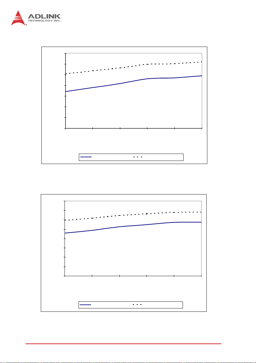
Intel® Core™ i7-2710QE (cPCI-6210)
70
60
50
40
30
20
Max. Air Inlet Temp. (°C)
10
0
12 15 18 21 24 27
Airflow Rate ( CFM)
100% CPU Loading 75% CPU Loading
Intel® Core™ i7-2710QE (cPCI-6210D)
80
70
60
50
40
30
20
Max. Air Inlet Temp. (°C)
10
0
12 15 18 21 24 27
Airflow Rate ( CFM)
100% CPU Loading 75% CPU Loading
14 Specifications
Page 29
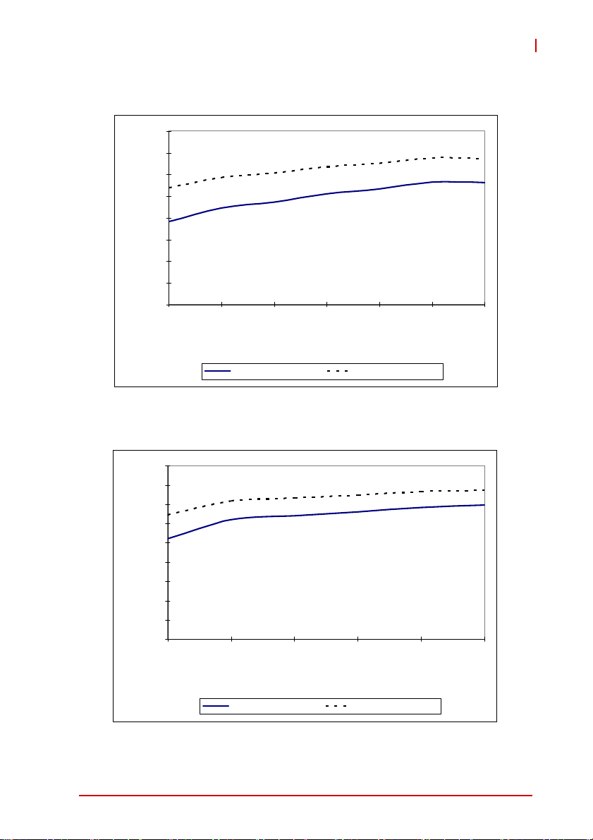
Intel® Core™ i5-2510E (cPCI-6210)
80
70
60
50
40
30
20
Max. Air Inlet Temp. (°C)
10
0
9 121518212427
Airflow Rate ( CFM)
100% CPU Loading 75% CPU Loading
Intel® Core™ i5-2510E (cPCI-6210D)
cPCI-6210
90
80
70
60
50
40
30
20
Max. Air Inlet Temp. (°C)
10
0
12 18 24 30 36 42
Airflow Rate ( CFM)
100% CPU Loading 75% CPU Loading
Specifications 15
Page 30

This page intentionally left blank.
16 Specifications
Page 31

3 Functional Description
The following sections describe the cPCI-6210 Series features
and functions.
3.1 Processor
Intel® Core™ i7 Processor
The 2nd Generation Intel® Core™ processor family mobile and
Intel® Celeron® processor family mobile are the next generation
of 64-bit, multi-core mobile processor built on 32- nanometer process technology. Based on a new micro-architecture, the processor is designed for a two-chip platform. The two-chip platform
consists of a processor and Platform Controller Hub (PCH). The
platform enables higher performance, lower cost, easier validation, and improved x-y footprint. The processor includes Integrated
Display Engine, Processor Graphics and Integrated Memory Controller.
The following table lists the processors supported by the
cPCI-6210 Series and their specifications.
Features Core™ i7-2710QE Core™ i7-2515E Celeron® B810
Clock 2.1GHz 2.5GHz 1.6GHz
Max. Single Core
Turbo Freq.
Last Level Cache 6MB 3MB 2MB
No. of
Cores/Threads
1
Max. Power (TDP
T
j, Max
Notes:
1. The highest expected sustainable power while running known
power intensive applications. TDP is not the maximum power
that the processor can dissipate.
2. Maximum junction temperature (T
ported operating temperature.
) 45W 35W 35W
2
3GHz 3.2GHz N/A
4/8 2/4 2/2
100°C 100°C 100°C
). The maximum sup-
j,Max
cPCI-6210
Functional Description 17
Page 32

Supported Technologies
X Intel® Virtualization Technology for Directed I/O (Intel® VT-d)
X Intel® Virtualization Technology (Intel® VT-x)
X Intel® Hyper-Threading Technology
X Intel® 64 Architecture
X Execute Disable Bit
X Intel® Turbo Boost Technology
Interfaces
X Two channels of DDR3 memory with a maximum of one
SO-DIMM per channel
X Memory DDR3 data transfer rates of 1066 MT/s, 1333
MT/s, and 1600 MT/s
X 64-bit wide channels
X DDR3 I/O Voltage of 1.5 V
X 1Gb, 2Gb, and 4Gb DDR3 DRAM technologies are sup-
ported for x8 and x16 devices
Z Using 4Gb device technologies, the largest memory
capacity possible is 16 GB, assuming dual-channel
mode with two x8, dual-ranked, un-buffered, non-ECC,
SO-DIMM memory configuration.
X The PCI Express port(s) are fully-compliant with the PCI
Express Base Specification, Revision 2.0.
X 5 GT/s point-to-point DMI interface to PCH is supported
X The Processor Graphics contains a refresh of the sixth gen-
eration graphics core
X enabling substantial gains in performance and lower power
consumption.
X DX10.1, DX10, DX9 support
X OGL 3.0 support
X FDI carries display traffic from the Processor Graphics in
the processor to the legacy display connectors in the PCH
18 Functional Description
Page 33

cPCI-6210
3.2 Chipset
Mobile Intel® QM67 Express Chipset
The cPCI-6210 Series is equipped with the Mobile Intel® QM67
Express Chipset, also referred to as PCH (Platform Controller
Hub), to provide extensive I/O support. Functions and capabilities
include:
X PCI Express Base Specification, Revision 2.0 support for up
to eight ports with transfer rate up to 5 GT/s
X ACPI Power Management Logic Support, Revision 4.0a
X Enhanced DMA controller, interrupt controller, and timer
functions
X Integrated Serial ATA host controllers with independent
DMA operation on up to six ports
X USB host interface with two EHCI high-speed USB 2.0 Host
controllers and two rate matching hubs provide support for
up to fourteen USB 2.0 ports
X Integrated 10/100/1000 Gigabit Ethernet MAC with System
Defense
X System Management Bus (SMBus) Specification, Version
2.0 with additional support for I2C devices
X Supports Intel® High Definition Audio
X Supports Intel® Rapid Storage Technology
X Supports Intel® Virtualization Technology for Directed I/O
X Integrated Clock Controller
X Analog and Digital Display ports
X Low Pin Count (LPC) interface
X Firmware Hub (FWH) interface support
X Serial Peripheral Interface (SPI) support
Functional Description 19
Page 34

3.3 PMC/XMC
The cPCI-6210D Series supports one PMC or XMC site for front
panel I/O expansion. The PMC site provides a maximum
32-bit/66MHz PCI bus link using a TI XIO2001 PCIe-to-PCI bridge
and PCIe x1 link. The PMC site supports +3.3V and 5V signaling.
The XMC site provides a x8 PCIe lane.
3.4 Intel® Turbo Boost Technology
Intel Turbo Boost Technology is a feature that allows the processor
to opportunistically and automatically run faster than its rated
operating core and/or render clock frequency when there is sufficient power headroom, and the product is within specified temperature and current limits. The Intel Turbo Boost Technology feature
is designed to increase performance of both multi-threaded and
single-threaded workloads. The processor supports a Turbo mode
where the processor can use the thermal capacity associated with
package and run at power levels higher than TDP power for
short durations. This improves the system responsiveness for
short, bursty usage conditions.
Turbo Mode availability is independent of the number of active
cores; however, the Turbo Mode frequency is dynamic and dependent on the instantaneous application power load, the number of
active cores, user configurable settings, operating environment,
and system design. If the power, current, or thermal limit is
reached, the processor will automatically reduce the frequency to
stay with its TDP limit.
3.5 Intel® Hyper-Threading Technology
Intel® Hyper-Threading Technology allows an execution core to
function as two logical processors. While some execution
resources (such as caches, execution units, and buses) are
shared, each logical processor has its own architectura l state with
its own set of general-purpose registers and control registers. This
feature must be enabled using the BIOS and requires operating
system support. Intel recommends enabling Hyper-Threading
Technology with Microsoft Windows 7, Vista, and XP, and disabling Hyper-Threading Technology using the BIOS for all previous versions of Windows operating systems.
20 Functional Description
Page 35

cPCI-6210
3.6 Trusted Platform Module
Upon request, the cPCI-6210 supports the Infineon SLB 96 35 TT
1.2 Trusted Plat form Mod ule (TPM), a se curity controller with cryp-
tographic functionality that provides users a secure environment in
e-commerce transactions and Internet communications.
The key features the TPM provides ar e:
X Hardware hash accelerator for SHA-1 algorithm.
X Advanced Crypto Engine (ACE) for asymmetric key opera-
tions (up to 2048-bit key length) to make hardware protection.
X Tick counter to extend the time requir ed to decipher th e key.
In addition to an encryption key created by the user, the TPM also
provides security features to protect the TPM itself:
X Over/Under-voltage detection to monitor the system stabil-
ity. If the voltage fluctuates dramatically, this function can
block the data transfer and lock the chip.
X Low/High frequency sensor to detect the IC clock fre-
quency. If the frequency fluctuates dramatically, this function can block the data transfer and lock the chip.
X Reset filter to filter reset signal in order to break the time se t
by tick counter is received.
X Memory encryption to protect memory.
X Physical shield in the IC to protect the die from intruding or
hacking by matching the data transferred on the 2 layer
metal shield on the IC. If the data is not matched, the IC
may be blocked.
The TPM does not support operation below 0ºC. Below this
temperature, the system may not boot. As a result, the
NOTE:
NOTE:
Functional Description 21
Extended T emperature versions of the cPCI-6210 are not available with TPM.
Page 36

3.7 Battery
The cPCI-6210 is equipped with a 3.0V "coin cell" lithium battery
for the Real Time Clock (RTC). The lithium battery must be
replaced with an identical battery or a battery type recommended
by the manufacturer. A Rayovac BR2032 with -40°C to +85°C
operating temperature support is equipped on board by default
3.8 Intel® Active Management Technology
Intel® Active Management Technology (Intel® AMT) is a hardware
based technology for remotely managing and securing PCs
out-of-band. Intel® AMT includes hardware-based remote management, security, power-management, and remote-configuration
features. Intel® AMT allows remote access to a system when traditional techniques and methods are not availa b l e.
22 Functional Description
Page 37

4 Board Interfaces
U6
This chapter describes the board layout, connector pin assignments, and jumper settings of the cPCI-6210 Series.
4.1 cPCI-6210(D) Series Board Layout
SW5/8/7/9/3/6
CN9
CN10
CN26
BT1
CN2
CN1
CN17
CN12
SW2
J5
CN15
J3
J2
cPCI-6210
U2
U27
J1
U2 CPU CN15 SATA port (7-pin)
U6 QM67 PCH CN17 CFast socket
U27 PCIe-to-PCI Bridge CN26 COM5 box header
CN1/2 DDR3 SO-DIMM sockets BT1 RTC Battery
CN9/10 DB-6210L2 connectors
(cPCI-6210D only)
J1-5 CompactPCI connectors
SW2 Clear CMOS Switch
CN12 DB-6920SAT connector SW3~10 DIP Switches
Figure 4-1: cPCI-6210(D) Series Board Layout
Board Interfaces 23
Page 38

4.2 cPCI-6210D Assembly Layout
The dual-slot width cPCI-6210D is comprised of the cPCI-6210
single-slot main board and the DB-6210L2 riser card to provide a
PMX/XMC site
DB-6210L2
Figure 4-2: cPCI-6210D Assembly Layout
24 Board Interfaces
Page 39

4.3 cPCI-6210(D) Front Panel
cPCI-6210
Status LEDs
cPCI-6210
Reset Button
cPCI-6210D
Reset Button
DisplayPort
KB/MS
PMC/XMC
DisplayPort
KB/MS
DVI-I
DVI-I
GbE 1/2/3
COM5
GbE 1/2/3
Figure 4-3: cPCI-6210(D) Front Panel Layout
USB 2.0
USB 2.0
COM1
COM1
Board Interfaces 25
Page 40

Status LEDs
WD HD
PW HS
RST
LED Color Condition Indication
Power
(PW)
Hot Swap
(HS)
HDD
(HD)
WDT
(WD)
Green
Blue
Red
Amber
Off System is off
On System is on
Off Handles closed, System is on
Fast Blink
On
Slow Blink
Preparing to shut down system
(LED: 0.1s on, 0.9s off)
Handles open and blade ready
to be removed
Voltages out of tolerance:
1
3.3V, 5V, 12V, 1.5V over ±5%
(LED: 2s on, 1s off)
Off No drive activity
Blinking
SATA HDD, CFast, CF data
read/write in process
Off No Watchdog event
Watchdog event alert
On/Blinking
(activity dependent on WDT
programming)
T able 4-1: cPCI-6210 Front Panel Status LED Descriptions
1. Disabled by default. See “OemSetBlueLEDLongBlinking” on
page 116.
26 Board Interfaces
Page 41

cPCI-6210
4.4 Connector Pin Assignments
Refer to “cPCI-6210(D) Series Board Layout” on page 23 and
“cPCI-6210(D) Front Panel Layout” on page 25 for connector locations
USB Connectors
Pin # Signal Name
1Vcc
2UV03UV0+
4GND
Table 4-2: USB Connector Pin Definition
PS/2 Keyboard/Mouse Port
Pin # Signal Function
1 KBDAT Keyboard Data
2MSDAT Mouse Data
3 GND Ground
4+5V Power
5 KBCLK Keyboard Clock
6 MSCLK Mouse Clock
Board Interfaces 27
Page 42

RJ-45 Gigabit Ethernet Connectors
Pin #
1 TX+ LAN_TX0+
2TX- LAN_TX03 RX+ LAN_TX1+
4 -- LAN_TX2+
5 -- LAN_TX26RX- LAN_TX17 -- LAN_TX3+
8 -- LAN_TX3+
Network link is not established
or system powered off
10 Mbps
100 Mbps
1000 Mbps
10BASE-T/
100BASE-TX
Ta ble 4-3: GbE Connector Pin Definitions
Status
Link OFF ON
Active OFF Blinking
Link Green ON
Active Green Blinking
Link Amber ON
Active Amber Blinking
1000BASE-T
Speed LED
(Green/Amber)
OFF OFF
81
Speed Activity
Activity LED
(Amber)
28 Board Interfaces
Page 43

COM1 Connector (DB-9)
Pin # RS-232 RS-422 RS-485
1DCD-L — —
2 RXD RXD- —
3 TXD TXD- TXD4DSR-L — —
5 Ground — —
6DSR-L — —
7 RTS-L TXD+ TXD+
8CTS-LRXD+ —
9— — —
Table 4-4: COM1 Connector Pin Definition
The COM1 RS-422/485 pin definitions are different from the
common DB-9 pin definitions. An RS-4 22/485 DB-9 male-female
NOTE:
NOTE:
adapter dongle is provided to allow compatibility with common
RS-422/485 pin definitions.
RS-422/485 Adapter Dongle
cPCI-6210
A DB-9 male-female adapter dongle is provided to allow compatibility with common RS-422/485 pin definitions
DB-9 (Female)
Signal Name
Pin #
NC 1 TXDRXD- 2 TXD+
TXD- 3 RXD+
NC 4 RXD-
NC 5 NC
NC 6 NC
TXD+ 7 NC
RXD+ 8 NC
NC 9 NC
T able 4-5: RS-422/485 Adapter Dongle Pin Definition
Board Interfaces 29
DB-9 (Male)
Signal Name
Page 44

COM1 Connector with RS-422/485 Dongle (DB-9)
Pin # RS-422 RS-485
1TXD-TXD2 TXD+ TXD+
3RXD+ —
4RXD- —
5— —
6— —
7— —
8— —
9— —
Table 4-6: COM1 Connector with RS-422/485 Dongle Pin Definition
COM5 Box Header
Pin # RS-232
1DCD-L
2DSR-L
3RXD
4RTS-L
5TXD
6CTS-L
7DTR-L
8RI-L
9 Ground
10 NC
12
910
Ta ble 4-7: COM5 Box Header Definition
30 Board Interfaces
Page 45

COM5 Connector (DB-9)
Pin # RS-232
1 DCD-L
2RXD
3TXD
4DSR-L
5Ground
6DSR-L
7RTS-L
8CTS-L
9RI-L
Table 4-8: COM5 Connector Pin Definition
The COM5 DB-9 front panel connector is only available on the
cPCI-6210D (8HP) version.
NOTE:
NOTE:
cPCI-6210
Board Interfaces 31
Page 46

DVI-I Connector
Pin # Signal Pin # Signal
1 TMDS Data2- 16 Hot Plug Detect
2 TMDS Data2+ 17 TMDS Data03 GND 18 TMDSData0+
4NC19GND
5NC20NC
6 DDC Clock [SCL] 21 NC
7 DDC Data [SDA] 22 GND
8 Analog vertical sync 23 TMDS Clock +
9 TMDS Data1- 24 TMDS Clock 10 TMDS Data1+ C1 Analog Red
11 GND C2 Analog Green
12 NC C3 Analog Blue
13 NC C4 Analog Horizontal Sync
14 +5 V Power C5 Analog GND Return
15 GND
Table 4-9: DVI-I Connector Pin Definition
32 Board Interfaces
Page 47

DisplayPort Connector
Pin # Signal Pin # Signal
1 CN_DP0_P 2 Ground
3 CN_DP0_N 4 CN_DP1_P
5 Ground 6 CN_DP1_N
7 CN_DP2_P 8 Ground
9 CN_DP2_N 10 CN_DP3_P
11 Ground 12 CN_DP3_N
13 CN_CAD-L 14 CN_CEC
15 CN_AUX_P 16 Ground
17 CN_AUX_N 18 DDP_HPD
19 Ground 20 P3V3
Table 4-10: DisplayPort Pin Definition
Serial ATA Connector (CN15)
Pin # Signal
1GND
2TX+
3TX4GND
5RX6RX+
7GND
Table 4-11: Serial ATA Connector Pin Definition
cPCI-6210
1
2
19
20
1
7
Board Interfaces 33
Page 48

CFast Socket (CN17)
Pin # Signal Name
Ground S1
SATA_TX-P S2
SATA_TX-N S3
Ground S4
SATA_RX-N S5
SAT A_RX-P S6
Ground S7
CFast_CDI P1
Ground P2
NC P3
NC P4
NC P5
NC P6
Ground P7
CFast_LED1 P8
CFast_LED2 P9
NC P10
NC P11
NC P12
P3V3 P13
P3V3 P14
Ground P15
Ground P16
CFast_CDO P17
24
1
S1P1
Table 4-12: CFast Socket Pin Definition
34 Board Interfaces
Page 49

Serial ATA Connector on DB-6920SAT
Pin # Signal
S1 GND
S2 TX+
S3 TXS4 GND
S5 RXS6 RX+
S7 GND
P1 NC
P2 NC
P3 NC
P4 GND
P5 GND
P6 GND
P7 5V
P8 5V
P9 5V
P10 GND
P11 NC
P12 GND
P13~P15 NC
cPCI-6210
S1
Signal
S7
P1
Power
P15
Table 4-13: DB-6920SAT SATA Connector Pin Definition
Board Interfaces 35
Page 50

DB-6920SAT Connector (CN12)
Signal Name Pin # Pin # Signal Name
GND 1 2 GND
GND 3 4 GND
GND 5 6 GND
GND 7 8 GND
GND 9 10 GND
GND 11 12 GND
GND 13 14 GND
GND 15 16 GND
GND 17 18 GND
GND 19 20 GND
GND 21 22 GND
GND 23 24 GND
GND 25 26 GND
GND 27 28 GND
GND 29 30 GND
P3V3 31 32 P5V
P3V3 33 34 P5V
P3V3 35 36 P5V
P3V3 37 38 P5V
P1V8 39 40 12V
P1V8 41 42 12V
P1V8 43 44 12V
GND 45 46 GND
GND 47 48 SATA-TXN0
GND 49 50 SATA-TXP0
SATA-RXN0 51 52 GND
SATA-RXP0 53 54 GND
GND 55 56 RESET#
GND 57 58 GND
GND 59 60 GND
1 2
59 60
Table 4-14: DB-6920SAT Connector Pin Definition
36 Board Interfaces
Page 51

PMC Connectors on DB-6210L2 (JN1, JN2)
cPCI-6210
Pin# JN1 Signal JN2 Signal
1 PMC_TCK P12V
2 N12V* PMC_TRST-L
3GND PMC_TMS
4 PCIX_INTA-L NC (PMC_TDO)
5 PCIX_INTB-L PMC_TDI
6PCIX_INTC-L GND
7PMC_MOD-L1 GND
8P5V NC
9 PCIX_INTD-L NC
10 NC NC
11 GND PMC_MOD-L2
12 P3V3_PMCAUX P3V3
13 CLK66_PCIX_PMC PMC_RST-L
14 GND PMC_MOD-L3
15 GND P3V3
16 PCIX_GNT-L0 PMC_MOD-L4
17 PCIX_REQ-L0 PMC_PME-L
18 P5V GND
19 PMC_VIO PCIX_AD30
20 PCIX_AD31 PCIX_AD29
21 PCIX_AD28 GND
22 PCIX_AD27 PCIX_AD26
23 PCIX_AD25 PCIX_AD24
24 GND PCIX_AD23
25 GND PMC_IDSEL
26 PCIX_CBE-L3 PCIX_AD23
27 PCIX_AD22 P3V3
28 PCIX_AD21 PCIX_AD20
29 PCIX_AD19 PCIX_AD18
30 P5V GND
31 PCIX_FRAME-L PCIX_AD16
32 PCIX_AD17 PCIX_CBE-L2
6364
12
Table 4-15: PMC Connector Pin Definitions
*Note: -12V signal not supported on JN1 pin 2. Contact ADLINK for more
information.
Board Interfaces 37
Page 52

Pin# JN1 Signal JN2 Signal
33 PCIX_FRAME-L GND
34 GND NC
35 GND PCIX_TRDY-L
36 PCIX_IRDY-L P3V3
37 PCIX_DEVSEL-L GND
38 P5V PCIX_STOP-L
39 PCIX_PCIXCAP PCIX_PERR-L
40 PCIX_LOCK-L GND
41 NC P3V3
42 NC PCIX_SERR-L
43 PCIX_PAR PCIX_CBE-L1
44 GND GND
45 PMC_VIO PCIX_AD14
46 PCIX_AD15 PCIX_AD13
47 PCIX_AD12 PCIX_M66EN
48 PCIX_AD11 PCIX_AD10
49 PCIX_AD9 PCIX_AD8
50 P5V P3V3
51 GND PCIX_AD7
52 PCIX_CBE-L0 NC
53 PCIX_AD6 P3V3
54 PCIX_AD5 NC
55 PCIX_AD4 NC
56 GND GND
57 PMC_VIO NC
58 PCIX_AD3 NC
59 PCIX_AD2 GND
60 PCIX_AD1 NC
61 PCIX_AD0 PCIX_ACK64-L
62 P5V P3V3
63 GND GND
64 PCIX_REQ64-L NC
Table 4-15: PMC Connector Pin Definitions (cont’d )
38 Board Interfaces
Page 53

cPCI-6210
XMC Connector on DB-6210L2
Pin# A B C D E F
1RXP RXN 3.3V NC NC VPWR
2 GND GND Not used GND GND PCIE_RST-L
3NC NC 3.3V NC NC VPWR
4 GND GND Not used GND GND Not used
5NC NC 3.3V NC NC VPWR
6 GND GND Not used GND GND +12V
7NC NC 3.3V NC NC VPWR
8 GND GND Not used GND GND -12V
9 NC NC Not used NC NC VPWR
10 GND GND Not used GND GND GA0
11 TXP TXN Not used NC NC VPWR
12 GND GND GA1 GND GND Not used
13 NC NC 3.3V NC NC VPWR
14 GND GND GA2 GND GND Not used
15 NC NC Not used NC NC VPWR
16 GND GND Not used GND GND Not used
17 NC NC Not used NC NC NC
18 GND GND Not used GND GND Not used
19 CK-P CK-N Not used Not used Not used Not used
Table 4-16: XMC Connector Pin Definition
Board Interfaces 39
Page 54

DB-6210L2 Connector (CN9)
Signal Name Pin # Pin # Signal Name
GND 2 1 GND
PCIE_A_RXP0 4 3 PCIE_A_TXP0
PCIE_A_RXN0 6 5 PCIE_A_TXN0
GND 8 7 GND
PCIE_A_RXP1 10 9 PCIE_A_TXP1
PCIE_A_RXN1 12 11 PCIE_A_TXN1
GND 14 13 GND
PCIE_A_RXP2 16 15 PCIE_A_TXP2
PCIE_A_RXN2 18 17 PCIE_A_TXN2
GND 20 19 GND
PCIE_A_RXP3 22 21 PCIE_A_TXP3
PCIE_A_RXN3 24 23 PCIE_A_TXN3
GND 26 25 GND
CLK-P 28 27 PCIE_RST-L
CLK-N 30 29 GND
GND 32 31 SML_DA T
XMC1_RST-L 34 33 SML_CLK
+12V 36 35 P5V_STB
+12V 38 37 P5V_STB
+12V 40 39 -12V
+5V 42 41 -12V
+5V 44 43 +3.3V
+5V 46 45 +3.3V
+5V 48 47 +3.3V
+5V 50 49 +3.3V
+5V 52 51 +3.3V
+5V 54 53 +3.3V
+5V 56 55 +3.3V
+5V 58 57 +3.3V
+5V 60 59 +3.3V
60
12
59
Table 4-17: DB-6210L2 Connector (CN9) Pin Definition
40 Board Interfaces
Page 55

DB-6210L2 Connector (CN10)
Signal Name Pin # Pin # Signal Name
GND 2 1 GND
PCIE_B_RXP0 4 3 PCIE_B_TXP0
PCIE_B_RXN0 6 5 PCIE_B_TXN0
GND 8 7 GND
PCIE_B_RXP1 10 9 PCIE_B_TXP1
PCIE_B_RXN1 12 11 PCIE_B_TXN1
GND 14 13 GND
PCIE_B_RXP2 16 15 PCIE_B_TXP2
PCIE_B_RXN2 18 17 PCIE_B_TXN2
GND 20 19 GND
PCIE_B_RXP3 22 21 PCIE_B_TXP3
PCIE_B_RXN3 24 23 PCIE_B_TXN3
GND 26 25 GND
PCIE_B_RXP4 28 27 PCIE_B_TXP4
PCIE_B_RXN4 30 29 PCIE_B_TXN4
GND 32 31 GND
PCIE_B_RXP5 34 33 PCIE_B_TXP5
PCIE_B_RXN5 36 35 PCIE_B_TXN5
GND 38 37 GND
PCIE_B_RXP6 40 39 PCIE_B_TXP6
PCIE_B_RXN6 42 41 PCIE_B_TXN6
GND 44 43 GND
PCIE_B_RXP7 46 45 PCIE_B_TXP7
PCIE_B_RXN7 48 47 PCIE_B_TXN7
GND 50 49 GND
XMC_PCIE-P 52 51 +3.3V
XMC-PCIE-N 54 53 +3.3V
GND 56 55 +3.3V
+12V 58 57 +3.3V
+12V 60 59 +3.3V
cPCI-6210
60
12
59
Ta ble 4-18: DB-6210L2 Connector (CN10) Pin Definition
Board Interfaces 41
Page 56

CompactPCI J1 Connector Pin Assignment
Pin Z A B C D E F
25 GND +5V REQ64# ENUM# +3.3V +5V GND
24 GND AD1 +5V V(I/O) AD0 ACK64# GND
23 GND P3V3 CPCI_AD4 CPCI_AD3 P5V CPCI_AD2 GND
22 GND CPCI_AD7 GND P3V3 CPCI_AD6 CPCI_AD5 GND
21 GND P3V3 CPCI_AD9 CPCI_AD8 CPCI_M66EN CPCI_CBE-L0 GND
20 GND CPCI_AD12 GND VIO CPCI_AD11 CPCI_AD 10 GND
19 GND P3V3 CPCI_AD15 CPCI_AD14 GND CPCI_AD13 GND
18 GND CPCI_SERR-L GND P3V3 CPCI_PAR CPCI_CBE-L1 GND
17 GND P3V3 IPMB_CLK IPMB_DAT GND CPCI_PERR-L GND
16 GND CPCI_DEVSEL-L GND VIO CPCI_STOP-L CPCI_LOCK-L GND
15 GND P3V3 CPCI_FRAME-L CPCI_IRDY-L NC CPCI_TRDY-L GND
12-14 GND Key Area Key
11 GND CPCI_AD18 CPCI_AD17 CPCI_AD16 GND CPCI_CBE-L2 GND
10 GND CPCI_AD21 GND P3V3 CPCI_AD20 CPCI_AD19 GND
9 GND CPCI_CBE-L3 NC CPCI_AD23 GND CPCI_AD22 GND
8 GND CPCI_AD26 GND VIO CPCI_AD25 CPCI_AD24 GND
7 GND CPCI_AD30 CPCI_AD29 CPCI_AD28 GND CPCI_AD27 GND
6 GND CPCI_REQ-L0 GND P3V3 CPCI_CLK0 CPCI_AD31 GND
5 GND NC NC CPCI_RESET-L GND CPCI_GNT-L0 GND
4 GND P5V_IPMB
3 GND CPCI_IRQA-L CPCI_IRQB-L CPCI_IRQC-L P5V CPCI_IRQD-L GND
2 GND cPCI_TCK-L P5V cPCI_TMS-L NC cPCI_TDI-L GND
1 GND P5V N12V cPCI_TRST-L P12V P5V GND
CPCI_HEALTHY-L
VIO NC NC GND
Table 4-19: CompactPCI J1 Connector Pin Definition
42 Board Interfaces
Page 57

cPCI-6210
CompactPCI J2 Connector Pin Assignment
Pin Z A B C D E F
22 GND GA4 GA3 GA2 GA1 GA0 GND
21 GND CLK6 GND NC NC NC GND
20 GND CLK5 GND NC GND NC GND
19 GND GND GND NC NC NC GND
18 GND NC NC NC GND NC GND
17 GND NC GND RSTBTN# REQ6# GNT6# GND
16 GND NC NC DEG# GND NC GND
15 GND NC GND FAL# REQ5# GNT5# GND
14 GND AD35 AD34 AD33 GND AD32 GND
13 GND AD38 GND V(I/O) AD37 AD36 GND
12 GND AD42 AD41 AD40 GND AD39 GND
11 GND AD45 GND V(I/O) AD44 AD43 GND
10 GND AD49 AD48 AD47 GND AD46 GND
9 GND AD52 GND V(I/O) AD51 AD50 GND
8 GND AD56 AD55 AD54 GND AD53 GND
7 GND AD59 GND V(I/O) AD58 AD57 GND
6 GND AD63 AD62 AD61 GND AD60 GND
5 GND CBE5# GND V(I/O) CBE4# PAR64 GND
4 GND V(I/O) NC CBE7# GND CBE6# GND
3 GND CLK4 GND GNT3# REQ4# GNT4# GND
2 GND CLK2 CLK3 SYSEN# GNT2# REQ3# GND
1 GND CLK1 GND REQ1# GNT1# REQ2# GND
Ta ble 4-20: CompactPCI J2 Co nnector Pin Definition
Board Interfaces 43
Page 58

CompactPCI J3 Pin Assignment
Pin Z A B C D E F
19 GND P5V P5V P12V P5V P5V GND
18 GND
17 GND
16 GND
15 GND
14 GND
13 GND
12 GND
11 GND
10 GND
9GND
8GND
7GND
6GND
5 GND GND GND NC GND GND GND
4GND
3GND
2GND
1GND
LAN3_D0+ LAN3_D0- GND LAN3_D2+ LAN3_D2- GND
LAN3_D1+ LAN3_D1- GND LAN3_D3+ LAN3_D3- GND
LAN4_D0+ LAN4_D0- GND LAN4_D2+ LAN4_D2- GND
LAN4_D1+ LAN4_D1- GND LAN4_D3+ LAN4_D3- GND
USB-OC4# USB-OC5# USB-OC6# USB-OC7# USB-OC8# GND
USB-P7+ USB-P7- GND USB-P8+ USB-P8- GND
USB-P5+ USB-P5- GND USB-P6+ USB-P6- GND
USB-P3+ USB-P3- GND USB-P4+ USB-P4- GND
USB-OC3# RGB-DDCCLK RGB-DDCDAT RGB-HSYNC RGB-VSYNC GND
COM3-CTS# COM3-RI# RGB-BLUE RGB-RED RGB-GREEN GND
COM3-RX COM3-TX COM3-DTR# COM3-DSR# COM3-RTS# GND
COM4-TX COM4-RX COM3-DCD# IPMB_CLK IPMB_DAT GND
SATA-RX4+ SATA-RX4- GND SATA-RX3+ SATA-RX3- GND
SATA-TX4+ SATA-TX4- GND SATA-TX3+ SATA-TX3- GND
KBDATA KBCLK NC MSDATA MSCLK GND
HDA_SDIN1 HDA_SDIN2 NC HDA_DOCK_EN# HDA_DOCK_RST# GND
HDA_RST# HDA_SYNC HDA_BIT_CLK HDA_SDOUT HDA_SDIN0 GND
Table 4-21: CompactPCI J3 Connector Pin Definition
High Definition audio
Keyboard/Mouse
Serial ATA
Serial ports
USB ports
Ethernet ports
RGB
44 Board Interfaces
Page 59

cPCI-6210
CompactPCI J5 Pin Assignment
Pin Z A B C D E F
22 GND NC LAN4_LINK_ACT# +3.3V LAN3_LINK_ACT# +3.3V GND
21 GND
20 GND
19 GND
18 GND
17 GND
16 GND
15 GND NC NC
14 GND NC NC GND
13 GND
12 GND
11 GND
10 GND
9GND
8GND
7 GND GND GND RTC GND GND GND
6GND
5 GND GND GND GND GND GND GND
4GND
3GND
2GND
1GND
LVDS_DATA2- LVDS_DATA2+ GND LVDS_CLK- LVDS_CLD+ GND
LVDS_DATA0- LVDS_DATA0+ GND LVDS_DATA1- LVDS_DATA1+ GND
DSKCHG# HDSEL# NC RDATA# WRPORT# GND
TRK0# WGATE# DETECT# WDATA# STEP# GND
DIR# NC GPIO8 DRVA# NC GND
MTR0# INDEX# GPIO7 NC DENSEL# GND
GPIO6 SATA-RX5+ SATA-RX5- GND
SATA-TX5+ SATA-TX5- GND
LAN4_100# LAN3_100# NC LAN3_1G# LAN4_1G# GND
DVI_DATA DVI_CLK DVI_HTPLG NC NC GND
TDC2+ TDC2- GND TLC+ TLC- GND
TDC0+ TDC0- GND TDC1+ TDC1- GND
GPIO1 GPIO2 GPIO3 GPIO4 GPIO5 GND
LVDS_DATA3- LVDS_DATA3+ NC LVDS_CLK LVDS_DATA GND
PCIE-CLK+ PCIE-CLK- GND RESET# NC GND
PCIE-TX3+ PCIE-TX3- GND PCIE-RX3+ PCIE-RX3- GND
PCIE-TX2+ PCIE-TX2- GND PCIE-RX2+ PCIE-RX2- GND
PCIE-TX1+ PCIE-TX1- GND PCIE-RX1+ PCIE-RX1- GND
PCIE-TX0+ PCIE-TX0- GND PCIE-RX0+ PCIE-RX0- GND
Ta ble 4-22: CompactPCI J5 Co nnector Pin Definition
PCI-Express x4
GPIO
DVI
Ethernet port
LVDS *
Serial ATA
Floppy
*LVDS function is not supported by default BIOS. Please
contact ADLINK if you require LVDS support.
NOTE:
NOTE:
Board Interfaces 45
Page 60

4.5 Switch and Jumper Settings
Refer to “cPCI-6210(D) Series Board Layout” on page 23 for
switch locations.
Load BIOS Default Switch (SW2)
Press switch SW2 to load the default BIOS settings.
Front/Rear VGA/LAN Selection Switch (SW3)
Switch SW3 sets the VGA and LAN3 outputs to the front panel
or to the rear panel of the RTM. The default VGA and LAN3
outputs are set to the front panel.
ON
ON
1
1 2
Switch Pin 1 Mode
1
2
Table 4-23: Front/Rear VGA Selection Switch Settings
ON Rear VGA output
OFF Front VGA output
ON Front LAN3 output
OFF Rear LAN3 output
3
2
SW5 & SW7 (Debug use only)
The switches SW5 & SW7 are for debugging purposes and
should be left in the default settings. The default setting of SW5
is all OFF; the default setting of SW7 is Pin 1 OFF and Pin 2
ON.
46 Board Interfaces
Page 61

cPCI-6210
Mode Switch (SW6)
Switch SW6 is a multi purpose switch that allows users to
define the board operating mode. Four pins independently control the mode setting. All are set to OFF by default.
ON
1 2
3 4
Pin# Status Description
ON
Not used.
Not used.
OFF
1
When the system does not include a CMM (Chassis
OFF
2
3OFF
OFF
4
Management
"without CMM mode".
When the system includes a CMM, set this pin to ON to allow
ON
IPMI to run in "with CMM mode".
For debugging purposes. Do not change the default setting (OFF).
The cPCI-6210 power on/off is state is controlled by the ejector
handle state.
Force the ejector handle state to "closed".
ON
Module), set this pin to OFF to allow IPMI to run in
Ta ble 4-24: Mode Switch Settings
Board Interfaces 47
Page 62

COM1/Debug Switch (SW8)
Switch SW8 sets the COM1 serial port as a standard RS-232
serial port or as an IPMI debugging port.
ON
1 2
3 4
Mode 1 2 3 4
RS-232 COM port (default) ON ON OFF OFF
IPMI debugging port OFF OFF ON ON
Table 4-25: COM1/Debug Switch Settings
COM1 Mode Selection Switches (SW9,SW10)
Switch SW9 sets the COM1 serial port to RS-232 or
RS-422/485 mode and SW10 sets COM1 to RS-422 or RS-485
mode. When the SW9 is set to RS-232 mode, SW10 has no
function.
ON
ON
1
1 2
Mode 1 2
RS-232 (default) Not Used ON
RS-422/485 Not Used OFF
3
2
Table 4-26: COM1 Mode Selection Switch SW9 Settings
Mode 1 2
RS-485 Not Used ON
RS-422 Not Used OFF
Table 4-27: COM1 Mode Selection Switch SW10 Settings
48 Board Interfaces
Page 63

5 Getting Started
This chapter describes the installation of the following component s
to the cPCI-6210 and rear transition modules:
X CFast card
X CompactFlash card
X 2.5” SATA hard drive
X PMC/XMC module installation
5.1 CPU and Heatsink
The cPCI-6210 Series comes with CPU and heatsink pre-installed.
Removal of heatsink/CPU by users is not recommended. Please
contact your ADLINK service representative for assistance.
5.2 CFast Card Installation
Installing a CFast card – cPCI-6210
1. A CFast card can be installed in the location indicated
below.
cPCI-6210
Getting Started 49
Page 64

2. Turn the board over (solder side up) and remove the two
screws securing the CFast card retention bracket as
indicated below.
3. Remove the CFast card retention bracket from the
board.
50 Getting Started
Page 65

cPCI-6210
4. Turn the board over (component side up), then align and
insert the CFast card into the slot until it is properly
seated.
5. Align the CFast card retention bracket with the screw
holes as indicated.
Getting Started 51
Page 66

6. Turn the board over (solder side up) and secure CFast
card retention bracket to the board with two screws.
7. The CFast card installation is now complete.
52 Getting Started
Page 67

cPCI-6210
5.3 CompactFlash Card Installation
A CompactFlash card can be installed on the cPCI-6210 Series
using the DB-6920CF CompactFlash adapter (ordering code
"DB-CF-SA"). Note that the CompactFlash adapter occupies the
same space as the 2.5” SATA drive and both ca nnot be inst alled at
the same time.
Installing a CF card – cPCI-6210
1. Locate the DB-6920CF CompactFlash adapter, CF
retention bracket and four screws in the CompactFlash
kit DB-CF-SA. The CompactFlash adapter can be
installed on the location indicated below.
Getting Started 53
Page 68

2. Align the CompactFlash adapter with the onboard SATA
connector (CN12) and press down firmly until it is properly seated.
3. Turn the board over (solder side down) and secure
adapter with two screws as shown.
54 Getting Started
Page 69

cPCI-6210
4. Turn the board over (component side up) and insert a
CompactFlash card into the slot on the adapter. Install
the CF retention bracket with two screws as shown.
Getting Started 55
Page 70

5.4 2.5” SATA Drive Installation
The cPCI-6210D provides space to install a slim type 2.5” SATA
drive.
Installing a SATA Drive
1. Locate the DB-6920SAT daughter board in the package
contents and connect it to 2.5” slim type drive. Mount th e
SATA drive onto the bracket as shown.
Drive Bracket
Make sure the adapter board is under the drive bracket to
avoid damaging the SATA drive connectors.
CAUTION:
56 Getting Started
DB-6920SAT
SATA Drive
Page 71

cPCI-6210
2. Secure the SATA drive onto the bracket with the four
screws provided in the package. This unit is now
referred to as the “drive assembly”.
3. Locate the board-to-board SATA connector (CN12) on
the cPCI-6210 as indicated below.
To install the drive assembly on the cPCI-6210D, the
DB-6210L2 must first be removed as described in Step 1 of
NOTE:
NOTE:
Getting Started 57
“Installing a PMC/XMC Module” on page60
Page 72

4. Align the drive assembly so that the connector on the
DB-6920SAT mates with the board-to-board connector
(CN12) on the cPCI-6210 as shown. Press down on the
DB-6920SAT until it is properly seated.
5. Secure the top side of the drive assembly with two
screws shown as below . Turn the board over (solder side
up) to continue securing the drive assembly.
Support the hard drive assembly to avoid damaging the SATA
connectors when turning the board over to proceed with Step 6.
CAUTION:
58 Getting Started
Page 73

cPCI-6210
6. Secu re the bottom side of the drive assembly with four
screws shown as below.
7. The SATA drive installation is now complete.
Getting Started 59
Page 74

5.5 PMC/XMC Module Installation
The 8HP width cPCI-6210D provides space to install a PMC or
XMC module.
Installing a PMC/XMC Module
1. Remove the four screws indicated below to disassemble
the DB-6210L2 daughter board from the cPCI-6210D.
2. Mount the PMC/XMC module to the DB-6210L2 and
secure it using four screws provided by PMC/XMC supplier from the solder side of the DB-6210L2.
60 Getting Started
Page 75

cPCI-6210
3. Mount the PMC/XMC assembly onto the cPCI-6210D
and secure the PMC/XMC assembly with the four
screws removed in S tep 1 as shown below .
Getting Started 61
Page 76

This page intentionally left blank.
62 Getting Started
Page 77

6 Driver Installation
The cPCI-6210 drivers can be found on the ADLINK All-In-One
DVD at X:\cPCI\cPCI-6210\ or from the ADLINK website
(http://www.adlinktech.com). ADLINK provides validated drivers for Windows XP Professional and Windows 7. We recommend
using these drivers to ensure compatibility. The VxWorks BSP can
be downloaded from the cPCI- 6210 product page on the ADLINK
website.
6.1 Driver Installation Procedure
The following describes the driver installation procedures for Windows XP.
1. Install the Windows operating system before installing any
driver. Most standard I/O device drivers are installed during
Windows installation.
In order to enable AHCI mode, you must pre-install the
Intel® Rapid Storage Technology driver using the F6 instal-
NOTE:
NOTE:
lation method described in the file F6Readme.txt, located
here: …\AHCI\Intel RST Driver Files_F6 Install_
32bit_10.1.0.1008.zip (not required for Windows 7).
cPCI-6210
2. Install the chipset driver by extracting and running the pro-
gram in ...\Chipset\Intel_Chipset_Device_Software
_AllOS_9.2.0.1015.zip.
3. Install the Microsoft .NET Framework utilities (required for the
graphics utility) by extracting and running the program in
...\Chipset\Microsoft_Net_Framework_v3.5_SP1.zip.
4. Install the graphics driver and utilities by extracting and run-
ning the program in ...\Graphics\Intel_HD_Graphics
_Family_WinXP_6.14.10.5313.zip.
5. Install the LAN drivers by extracting and running the program
in …\LAN\Intel_82574L_Gigabit_Network_WINXP
_11.4.7.0.zip.
6. Install the Intel Rapid Storage Technology Utility by extract-
ing and running the program in …\AHCI\
Intel_Rapid_Storage_Technology_10.1.0.1008.zip
Driver Installation 63
.
Page 78

7. Install the TPM driver by extracting and running the program in
…\TPM\Infineon_Trusted_Platform_Module_2.1.1.0.zip.
8. Install the audio driver and utilities by extracting and running
the program in …\Audio\RealTek_High_Definition_Audio
_WINXP_5.10.0.6029.zip.
9. Install the Intel® Management Engine Interface driver by following the steps below:
Z R-click on My Computer, select Manage, and open the
Device Manager.
Z Under Other Devices you will see a "question mark" next
to PCI Simple Communication Controller. R-click on
PCI
Simple Communication Controller and click on Update
Driver to start the Hardware Update Wizard.
Z When asked to let Windows Update search for software ,
select "No, not at this time" and click
64 Driver Installation
Next.
Page 79

cPCI-6210
Z Select "Install from a list or specific location (Advanced)"
and click
Z Extract the contents of …\cPCI-6210\Chipset\Intel
Next.
_Management_Engine_Interface_AllOS_7.0.0.1144.zip.
Select "Search for the best driver in these locations" and
"Include this location in the search". Click
Browse and navigate to the folder "MEI" where you extracted the contents of
the zip file, and then click
OK. Click Next to continue.
Z When driver installation has completed, click Finish to
close the wizard.
Driver Installation 65
Page 80

This page intentionally left blank.
66 Driver Installation
Page 81

7 Utilities
7.1 Watchdog Timer
This section describes the operation of the cPCI-6210’s watchdog
timer (WDT). The primary function of the WDT is to monitor the
cPCI-6210's operation and to reset the system if a software application fails to function as prog rammed. The following WDT functions may be controlled using a software application:
X enabling and disabling
X reloading timeout value
The cPCI-6210 custom WDT circuit is implemented using the
internal IO of the ITE Super I/O IT8783 which is at address 2Eh of
LPC. The basic functions of the WDT include:
X Starting the timer countdown
X Enabling or disabling WDT
X Enabling or disabling WDT countdown LED ON
X Reloading the timeout value to keep the watchdog from timing
out
X Setting the range of the timeout period from 1 to 15300 seconds
or minutes
X Sending a RESET signal to the system when the watchdog
times out
cPCI-6210
Using the Watchdog in an Application
The following section describes using the WDT functions in an
application. The WDT reset function is explained in the previous
section. This can be controlled through the registers in the
cPCI-6210's Super I/O.
An application using the reset fe ature enab les the watch dog func tion, sets the count-down period, and reloads the timeout value
periodically to keep it from resetting the system. If the timer countdown value is not reloaded, the watchdog resets the system hardware after its counter reaches zero.
Utilities 67
Page 82

For a detailed programming sample, refer to the sample code provided on the ADLINK All-In-One CD. You can find it in the following
directory: X:\cPCI\cPCI-6210\WDT.
Sample Code
The sample program written in C shown below offers an interactive
way to test the Watchdog Timer under DOS.
#include<stdio.h>
#include<dos.h>
#define IT8783_ID1 0x87
#define IT8783_ID2 0x83
static unsigned int IT8783_ioPort = 0x2e;
//Check index port
void Enter_IT8783_Config(unsigned int flag)
{
if(flag) IT8783_ioPort = 0x4e;
switch(IT8783_ioPort)
{
case 0x2E: //Address port = 0x2E, enter
keys = 0x87, 0x01, 0x55, 0x55
outportb(0x2E, 0x87);
outportb(0x2E, 0x01);
outportb(0x2E, 0x55);
outportb(0x2E, 0x55);
break;
case 0x4E: //Address port = 0x4E, enter
keys = 0x87, 0x01, 0x55, 0xAA
outportb(0x4E, 0x87);
outportb(0x4E, 0x01);
outportb(0x4E, 0x55);
outportb(0x4E, 0xAA);
break;
default:
break;
}
}
68 Utilities
Page 83

cPCI-6210
//Exit index port
void Exit_IT8783_Config(unsigned int flag)
{
if(flag) IT8783_ioPort = 0x4e;
outportb(IT8783_ioPort, 0x02);
outportb(IT8783_ioPort+1, 0x02);
}
//Check chip
void Get_IT8783_ID(unsigned int &ID1, unsigned int &ID2)
{
outportb(IT8783_ioPort, 0x20);
ID1 = inportb(IT8783_ioPort+1);
outportb(IT8783_ioPort, 0x21);
ID2 = inportb(IT8783_ioPort+1);
}
//WDT and LED program
void IT8783_3_WDTRun(unsigned int count_value, unsigned
int PLEDflag) //for cPCI-6510
{
unsigned long tempCount;
unsigned int registerValue;
outportb(IT8783_ioPort, 0x07);
outportb(IT8783_ioPort+1, 0x07); // Device
7
outportb(IT8783_ioPort, 0xf8);
outportb(IT8783_ioPort+1, 0x00); // PLED
mapping to nothing, disable PLED function
if(PLEDflag == 1)
{
outportb(IT8783_ioPort, 0x2D);
registerValue = inportb(IT8783_ioPort +
1);
registerValue |= 0x01; // set
Pin109 is GPIO function GP60
outportb(IT8783_ioPort+1, registerValue);
Utilities 69
Page 84

outportb(IT8783_ioPort, 0xC5);
registerValue = inportb(IT8783_ioPort +
1);
registerValue &= 0xfe; // set GP60
is alternate function
outportb(IT8783_ioPort+1, registerValue);
outportb(IT8783_ioPort, 0xCD);
registerValue = inportb(IT8783_ioPort +
1);
registerValue |= 0x01; // set
GP60 is output
outportb(IT8783_ioPort+1, registerValue);
outportb(IT8783_ioPort, 0xf8);
outportb(IT8783_ioPort+1, 0x30); /
/ PLED mapping to GP60
outportb(IT8783_ioPort, 0xf9);
registerValue = inportb(IT8783_ioPort +
1);
registerValue |= 0x02;
registerValue &= 0xfb;
outportb(IT8783_ioPort+1, registerValue);
}
outportb(IT8783_ioPort, 0x71);
registerValue = inportb(IT8783_ioPort + 1);
registerValue |= 0xD0; // set
Mouse & Keyboard interrupt Enable
outportb(IT8783_ioPort+1, registerValue);
outportb(IT8783_ioPort, 0x73);
outportb(IT8783_ioPort+1, count_value); // set
WDT count LSB
tempCount = tempCount >> 8;
outportb(IT8783_ioPort, 0x74);
outportb(IT8783_ioPort+1, count_value); // set
WDT count MSB
if(count_value >= 60)
{
outportb(IT8783_ioPort, 0x72);
registerValue = inportb(IT8783_ioPort+1);
70 Utilities
Page 85

cPCI-6210
registerValue &= 0x8f;
registerValue |= 0x10; //enable WDT output
through PowerOK!
outportb(IT8783_ioPort+1, registerValue);
// set WDT count is minute
tempCount = count_value / 60;
if((count_value%60) > 30)
tempCount++;
if(tempCount > 65535)
tempCount = 65535;
printf("WDT timeout in %d minutes.\n",
tempCount);
}
else
{
outportb(IT8783_ioPort, 0x72);
registerValue = inportb(IT8783_ioPort+1);
registerValue |= 0x80;
tempCount = count_value;
if(tempCount != 0)
{
printf("WDT timeout in %d
seconds.\n", tempCount);
registerValue |= 0x40; //Enable
WDT output through KBRST
}
else
{
printf("WDT is Disabled.\n");
registerValue &= 0xbf; //Disable
WDT output through KBRST
}
outportb(IT8783_ioPort+1, registerValue);
// set WDT count is second
}
}
Utilities 71
Page 86

7.2 Using the Trusted Platform Module
This section describes the operation of the cPCI-6210’s Trusted
Platform Module (TPM).
Enabling TPM in BIOS
The TPM is set to "Disabled" by default. Users wishing to use the
TPM must first enable it in BIOS as follows:
TPM is not supported by default. If you require TPM for your
application, please contact your sales representative to order
NOTE:
NOTE:
a model that supports TPM.
1. Under the "Advanced" section in BIOS, choose "Trusted
Computing".
2. Set "TPM Support" to Enabled.
72 Utilities
Page 87

cPCI-6210
3. Set "TPM State" Enabled. Save settings and exit BIOS.
Using the TPM Utility
A utility for managing the TPM settings, the Infineon Security Platform Settings Tool, is provided with the TPM driver located on the
All-In-One DVD in the following directory:
X:\cPCI\cPCI-6210\TPM. Make sure you have installed the TPM
driver as described in 6.1 Driver Installation Procedure on
page 63.
1. After the driver is installed, click on Start > Programs >
Infineon Security Platform Solution > Manage Security
Platform to run the utility.
Utilities 73
Page 88

2. The Infineon Security Platform Settings Tool is shown in
the screen capture below.
3. Click on the "User Settings" tab, then follow the on
screen instructions to build a security platform.
74 Utilities
Page 89

cPCI-6210
4. Prepare a removable media to store important passwords and data and follow the on screen instructions.
Utilities 75
Page 90

7.3 BIOS Recovery
The cPCI-6210 Series features AMI® EFI BIOS with BIOS recovery. If the BIOS becomes corrupted and you are unable to boot
your system, the system will sound 4 beeps. Follow the instructions below to re-flash the BIOS and recover the system.
1. Download the BIOS recovery file "C6210000.ROM" from the
product website at:
www.adlinktech.com/PD/web/PD_detail.php?cKind=&pid=1013
2. Prepare a bootable USB flash drive and copy the recovery file "C6210000.ROM" to the root directory.
3. Insert the USB flash drive into the cPCI-6210 and power
up the system.
4. The system will sound 4 beeps to indicate boot failure,
and then it will sound 2 beeps to indicate it is entering
Recovery Mode. You will see the screen below:
5. Select "Proceed with flash update" and press Enter.
76 Utilities
Page 91

cPCI-6210
6. During the BIOS recovery process, you will see the following:
7. After the flash update is completed, power down the system
and restart. The system should now boot up normally.
After BIOS recovery, follow the instructions in Section 7.4 or
Section 7.5 to restore your original BIOS version.
NOTE:
NOTE:
Utilities 77
Page 92

7.4 BIOS Update - DOS Method
Follow the instructions below to upda te the BIOS or r estore a previous BIOS version using a DOS bootable storage device.
1. Download the required BIOS file from the product website:
www.adlinktech.com/PD/web/PD_detail.php?cKind=&pid=1013
2. Prepare a DOS bootable floppy disk or USB flash drive
and unzip the contents of the BIOS file to the disk
3. Boot the system using the flopp y disk or USB drive prepared above and run the file pBIOS.bat
4. Restart the system (if requested)
7.5 BIOS Update - ADLINK BIOS Updater Method
The ADLINK BIOS updater is a BIOS flash application embedded
in the EFI firmware volume. With the ADLINK BIOS updater, you
can update the system BIOS without first having to enter an operating system (e.g. MS-DOS or Windows). To access the ADLINK
BIOS updater, press the <F9> key during POST. The new BIOS
file can be saved to any storage device that has been formatted
with the F AT12/16/32 file system (e.g. hard drive, USB flash drive).
Updating the BIOS
The following procedure assumes that you have saved the new
BIOS ROM file to a USB flash drive.
1. Insert the USB flash drive containing the new BIOS file
into the USB target system. Boot up the system and
press the <F9> key during POST to enter the BIOS
Updater. You will be presented with a menu of storage
devices. Select the USB flash drive with the new BIOS
file using the up or down arrow keys and press <Enter>.
(In the example screen capture below, only one storage
device has been detected.)
78 Utilities
Page 93

cPCI-6210
2. The BIOS Updater will display the contents of the
selected storage device. Navigate to the desired BIOS
ROM file and press <Enter>. If the file has been saved in
a subdirectory, select the subdirectory and press
<Enter> to view its contents.
3. After you have selected the desired BIOS ROM file, the
BIOS Updater will ask you to confirm that you wish to
update the BIOS on your target system. Select "Yes" and
press <Enter> to begin the BIOS update. The progress
of the BIOS update will be displayed on screen.
Do not turn off or restart the system while the system is
reading/updating the BIOS.
CAUTION:
Utilities 79
Do not remove the USB flash drive or hard drive while the
system is updating the BIOS.
Page 94

4. After the update process is complete, system will automatically reboot.
80 Utilities
Page 95

8 BIOS Setup Utility
The following chapter describes basic navigation for the
AMIBIOS®8 BIOS setup utility.
8.1 Starting the BIOS
To enter the setup screen, follow these steps:
1. Power on the motherboard
2. Press the < Delete > key on your keyboard when you
see the following text prompt:
< Press DEL to run Setup >
3. After you press the < Delete > key, the main BIOS setup
menu displays. You can access the other setup screens
from the main BIOS setup menu.
cPCI-6210
Note: In most cases, the < Delete > key is used to invoke the setup
screen. There are several cases that use other keys, such as
< F1 >, < F2 >, and so on.
BIOS Setup Utility 81
Page 96

Setup Menu
The main BIOS setup menu is the first screen that you can navigate. Each main BIOS setup menu option is described in this
user’s guide.
The Main BIOS setup menu screen has two main frames. The left
frame displays all the options that can be configured. "Grayed"
options cannot be configured, "Blue" options can be.
The right frame displays the key legend. Above the key legend is
an area reserved for a text message. When an option is selected
in the left frame, it is highlighted in white. Often a text message will
accompany it.
82 BIOS Setup Utility
Page 97

cPCI-6210
Navigation
Note: There is a hot key legend located in the r ight frame on most
setup screens.
Keyboard Commands
Enter Selects the highlighted option or submenu.
< > The Left and Right "Arrow" keys allow you to select a setup
screen.
^ v The Up and Down "Arrow" keys allow you to select a setup
screen.
+ - The Plus and Minus keys allow you to change the field value
Tab Moves the cursor to the next configurable item or to the next
Esc The Esc key allows you to discard any changes you have
BIOS Setup Utility 83
of a particular setup item.
field.
made and exit the Setup menu. Press the Esc key to exit
the Setup menu without saving your changes. Press the
Enter key to discard changes and exit. You can also use the
"Arrow" keys to select Cancel and then press the Enter key
to abort this function and return to the previous screen.
Page 98

8.2 Main Setup
When you first enter the Setup Utility , you will enter the Main setup
screen. You can always retu rn to th e Main setup screen by selecting the Main tab. There are two Main Setup options. They are
described in this section. The Main BIOS Setup screen is shown
below.
System & Board Info
BIOS Vendor
Displays the BIOS vendor.
Core Version
Displays the BIOS core version.
Project Version
Displays the current BIOS revision.
Build Data
Displays the BIOS build data.
System Language
Displays the system default language (English only).
84 BIOS Setup Utility
Page 99

cPCI-6210
System Time/System Date
Use this option to change the system time and date. Highlight System Time or System Date using the < Arrow > keys. Enter new values using the keyboard. Press the < Tab > key or the < Arrow >
keys to move between fields. The date must be entered in
MM/DD/YY format. The time is entered in HH:MM:SS format.
Note: The time is in 24-hour format. For example, 5:30 A.M. ap-
pears as 05:30:00, and 5:30 P.M. as 17:30:00.
BIOS Setup Utility 85
Page 100

8.3 Advanced BIOS Setup
Select the Advanced tab from the setup screen to enter the
Advanced BIOS Setup screen. You can select any of the items in
the left frame of the screen, such as SuperIO Configuration, to go
to the sub menu for that item. You can display an Advanced BIOS
Setup option by highlighting it using the < Arrow > keys. The
Advanced BIOS Setup screen is shown below.
The sub menus are described on the following pages.
Launch PXE OpROM
Boot option for legacy network devices. Options: Enabled, Disabled.
Launch Storage OpROM
Boot option for legacy mass storage devices with Option ROM.
Options: Enabled/Disabled.
86 BIOS Setup Utility
 Loading...