

ADLINK cPCI-3971 User Manual
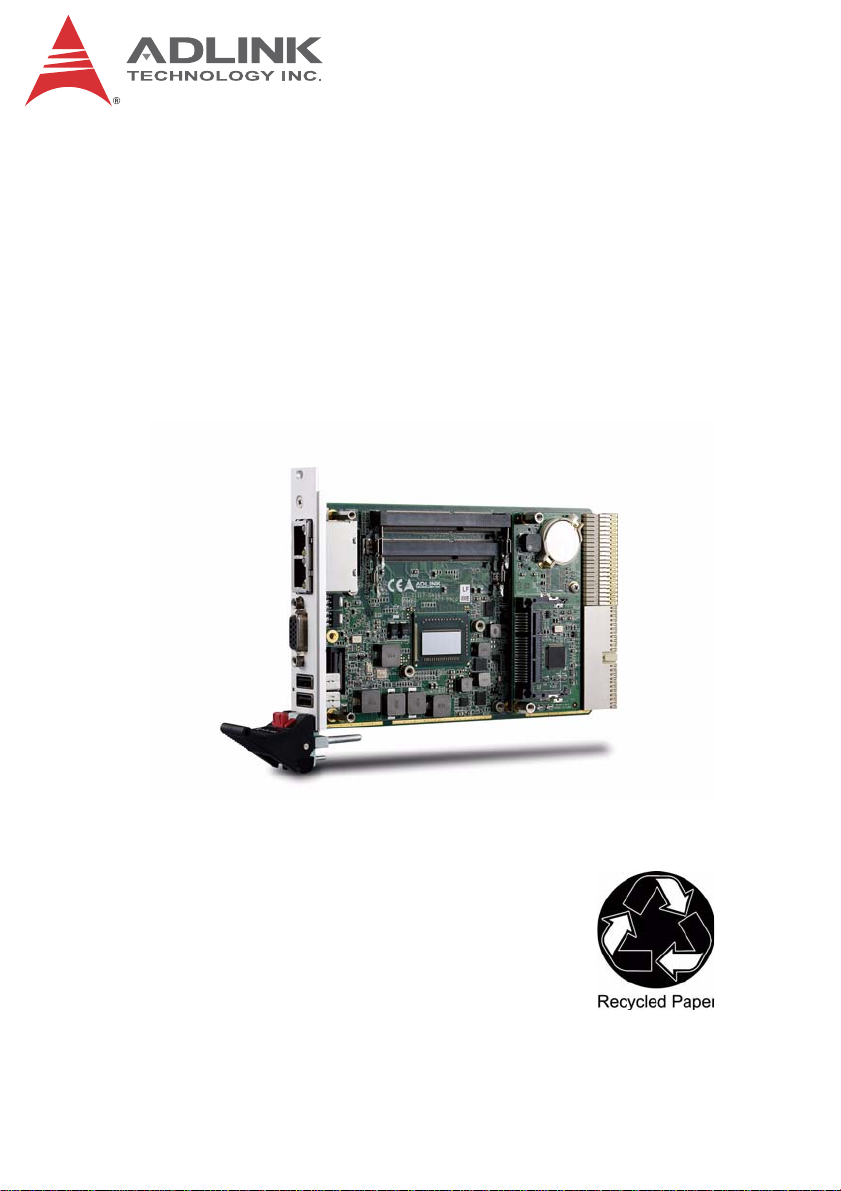
cPCI-3970/3971 Series
Performance 3U CompactPCI® PlusIO
Intel® Core™ i7 Processor Blade
User’s Manual
Manual Rev.: 2.02
Revision Date: March 29, 2013
Part No: 50-15078-1020
Advance Technologies; Automate the World.
Revision History
Revision Release Date Description of Change(s)
2.00 2011/09/15 Initial release
2.01 2012/11/16
2.02 2013/03/29
Add “Q”, “L” and “M” models; add Gold Cap
support
Correct “3.3V/5V” column headings in power
consumption tables

cPCI-3970
Preface
Copyright 2011-13 ADLINK Technology Inc.
This document contains proprietary infor mation protected by cop yright. All rights are reserved. No part of this manual may be reproduced by any mechanical, electronic, or other means in any form
without prior written permission of the manufacturer.
Disclaimer
The information in this document is subject to change without prior
notice in order to improve reliability, design, and function and does
not represent a commitment on the part of the manufact ur er.
In no event will the manufacturer be liable for direct, indirect, special, incidental, or consequential damages arising out of the use or
inability to use the product or documentation, even if advised of
the possibility of such damages.
Environmental Responsibility
ADLINK is committed to fulfill its social responsibility to global
environmental preservation through compliance with the European Union's Restriction of Hazardous Substances (RoHS) directive and Waste Electrical and Electronic Equipment (WEEE)
directive. Environmental protection is a top priority for ADLINK.
We have enforced measures to ensure th at our products, manufacturing processes, components, and raw materials have as little
impact on the environment as possible. When produ ct s ar e at th eir
end of life, our customers are encouraged to dispose of them in
accordance with the product disposal and/or recovery programs
prescribed by their nation or company.
Trademarks
Product names mentioned herein are used for identification purposes only and may be trademarks and/or registered trademarks
of their respective companies.
Preface iii

Using this Manual
Audience and Scope
The cPCI-3970 User’s Manual is intended for hardware
technicians and systems operators with knowledge of installing,
configuring and operating industrial grade single boar d computers.
Manual Organization
This manual is organized as follows:
Chapter 1, Introduction: Introduces the cPCI-3970, its features,
block diagrams, and package contents.
Chapter 2, Specifications: Presents detailed specification infor-
mation, power consumption, and technical drawings.
Chapter 3, Functional Description: Describes the cPCI-3970
main functions.
Chapter 4, Board Interfaces: Describes the cPCI-3970 board
interfaces.
Chapter 5, Getting Started: Describes the installation of compo-
nents to the cPCI-3970 and rear transition modules.
Chapter 6, Driver Installation: Provides information on how to
install the cPCI-3970 device drivers under Windows XP.
Chapter 7, Utilities: Describes the utilities of the cPCI-3970,
including watchdog timer and Trusted Platform Module.
Chapter 8, BIOS Setup Utility: Describes basic navigation for the
AMI EFI BIOS setup utility.
Chapter 9, IPMI User Guide: Provides information on the base-
board management controller (BMC) of the Intelligent Platform
Management Interface (IPMI).
Important Safety Instructions: Presents safety instructions all
users must follow for the proper setup, installation and usage of
equipment and/or software.
Getting Service: Contact information for ADLINK’s worldwide
offices.
iv Preface
cPCI-3970
Conventions
Take note of the following conventions used throughout this
manual to make sure that users perform certain tasks and
instructions properly.
Additional information, aids, and tips that help users perform
tasks.
NOTE:
NOTE:
Information to prevent minor physical injury, component damage, data loss, and/or program corruption when trying to com-
CAUTION:
WARNING:
plete a task.
Information to prevent serious physical injury, component
damage, data loss, and/or program corruption when trying to
complete a specific task.
Preface v

This page intentionally left blank.
vi Preface

cPCI-3970
Table of Contents
Revision History...................................................................... ii
Preface.................................................................................... iii
List of Figures........................................................................ xi
List of Tables........................................................................ xiii
1 Introduction ........................................................................ 1
1.1 Overview.............................................................................. 1
1.2 Features............................................................................... 1
1.3 Model Number Decoder....................................................... 2
1.4 Package Contents ............................................................... 5
2 Specifications..................................................................... 7
2.1 cPCI-3970 Processor Blade Specifications.................. .... ... 7
2.2 cPCI-R3P00(T) RTM Specifications.................................. 11
2.3 Block Diagrams.................................................................. 12
2.4 I/O Connectivity Table ....................................................... 19
2.5 Power Requirements.................... ... .... ... ... ... ... .... ... ... ... .... . 20
2.6 Thermal Requirements.................... .... ... ... ... ... .... ... ... ... .... . 22
3 Functional Description .................................................... 23
3.1 Processors......................................................................... 23
3.2 Platform Controller Hub ..................................................... 25
3.3 PMC/XMC.......................................................................... 25
3.4 Intel® Turbo Boost Technology......................................... 26
3.5 Intel® Hyper-Threading Technology.................................. 26
3.6 Trusted Platform Module ................................................... 26
3.7 Battery ............................................................................... 27
3.8 BIOS Recovery.................................................................. 28
Table of Contents vii

4 Board Interfaces................................................................ 29
4.1 cPCI-3970 Series Board Layout ..................................... ... 29
4.2 cPCI-3970 Blade Assembly Layout ................................... 30
4.3 cPCI-3970D Blade Assembly Layout................................. 31
4.4 cPCI-3970G Blade Assembly Layout................................. 32
4.5 cPCI-3970, cPCI-3970D, cPCI-3970G Faceplate.............. 33
4.6 cPCI-3970S, cPCI-3970P, cPCI-3970U Front Panel......... 34
4.7 cPCI-3970L, cPCI-3970M, cPCI-3970Q Front Panel......... 35
4.8 cPCI-R3P00(T) RTM Board Layout................................... 37
4.9 cPCI-R3P00(T) RTM Faceplate......................................... 38
4.10 Connector Pin Assignments............................................... 39
4.11 Jumper Settings................................................................. 65
5 Getting Started.................................................................. 67
5.1 CPU and Heatsink ............................................................. 67
5.2 Memory Module Installation............................................... 68
5.3 SATA Drive Installation...................................................... 70
5.4 CompactFlash Installation.................................................. 71
5.5 Converting from CF to CFast Slot...................................... 72
5.6 PMC/XMC Card Installation............................................... 77
5.7 Installing the cPCI-3970 to the Chassis............................. 81
5.8 RTM Installation - cPCI-R3P00(T)..................................... 82
6 Driver Installation.............................................................. 83
6.1 cPCI-3970 Drivers.............................................................. 83
6.2 USB-to-Serial Converter Driver (RTM) .............................. 86
6.3 LAN Driver for cPCI-R3P00T............................................. 90
7 Utilities............................................................................... 91
7.1 Watchdog Timer................................................................. 91
7.2 Using the Trusted Platform Module ................................... 97
7.3 BIOS Recovery........................ .... ... ... ... ........................... 101
7.4 BIOS Update...................................... .............................. 103
viii Table of Contents

cPCI-3970
8 BIOS Setup Utility........................................................... 105
8.1 Starting the BIOS....................... ... ... .... ... ... ... ... .... ... ... ...... 105
8.2 Main Setup.......... ... .... ... ... ... .... ... ... ................................... 108
8.3 Advanced BIOS Setup..................................................... 110
8.4 Chipset Configuration ...................................................... 120
8.5 Boot Configuration........................................................... 124
8.6 Security Setup ................................................................. 125
8.7 Save & Exit...................................................................... 126
9 IPMI User Guide.............................................................. 129
9.1 Introduction...................................................................... 129
9.2 Summary of Commands Supported by BMR-AVR-cPCI. 129
9.3 OEM Commands Summary Table................................... 133
9.4 CompactPCI Address Map .............................................. 137
9.5 Communications with IPMC............................................. 137
9.6 IPMI Sensors List............................................................. 138
9.7 Relevant Documents ....................................................... 139
Important Safety Instructions............................................ 141
Getting Service.................................................................... 143
Table of Contents ix

This page intentionally left blank.
xTable of Contents

cPCI-3970
List of Figures
Figure 2-1: cPCI-3970 Blade Functional Block Diagram..................12
Figure 2-2: DB-3610L2 Daughter Board Func. Block Diagram........13
Figure 2-3: DB-3970L2 Daughter Board Func. Block Diagram........14
Figure 2-4: DB-LANL2-S Daughter Board Func. Block Diagram..... 15
Figure 2-5: DB-Max Daughter Board Func. Block Diagram.............16
Figure 2-6: cPCI-R3P00 RTM Func. Block Diagram............ ...... .... .. 17
Figure 2-7: cPCI-R3P00T RTM Func. Block Diagram .....................18
Figure 4-1: cPCI-3970 Series Board Layout....................................29
Figure 4-2: cPCI-3970 Blade Assembly Layout ...............................30
Figure 4-3: cPCI-3970D Blade Assembly Layout.............................31
Figure 4-4: cPCI-3970G Blade Assembly Layout ............................32
Figure 4-5: cPCI-3970(D/G) Front Panel Layout..............................33
Figure 4-6: cPCI-3970S/P/U Front Panel Layout............................. 34
Figure 4-7: cPCI-3970L/M/Q Front Panel Layout.............................35
Figure 4-8: cPCI-R3P00 RTM Board Layout........................ ... ... .... .. 37
Figure 4-9: cPCI-R3P00(T) RTM Front Panel..................................38
Figure 7-1: Example procedure for configuring the WDT ................ 95
List of Figures xi

This page intentionally left blank.
xii List of Figures

cPCI-3970
List of Tables
Table 2-1: cPCI-3970 Processor Blade Specifications.....................7
Table 2-2: cPCI-R3P00(T) RTM Specifications..............................11
Table 4-1: cPCI-3970 Front Panel System LED Descriptions ........ 36
Table 4-2: USB Pin Definition......................................................... 39
Table 4-3: VGA Pin Definition ... ... ... .... ... ... ... .... ... ... ... ... .... ... ... .........39
Table 4-4: RJ-45 GbE Pin Definitions.............................................40
Table 4-5: LAN LED Status Definitions........................................... 40
Table 4-6: PS/2 Keyboard/Mouse Pin Definition.............................41
Table 4-7: cPCI-3970D/P COM1 (DB-9) Pin Definition...................41
Table 4-8: cPCI-3970D/P COM1 Mode Selection Switch Settings. 42
Table 4-9: cPCI-3970G/U COM1 (RJ-45) Pin Definition................. 43
Table 4-10: cPCI-3970G/U COM1 (DB-9 adapter) Pin Definition.....43
Table 4-11: RS-422/485 Adapter Dongle Pin Definition ................... 44
Table 4-12: cPCI-3970D/P COM1 Dongle Pin Definition.................. 44
Table 4-13: cPCI-3970G/U COM2 Pin Header Definition..... ... ... .... .. 45
Table 4-14: cPCI-R3P00 RTM COM4 Pin Definition ........................ 45
Table 4-15: cPCI-R3P00(T) RTM COM5 Pin Definition.................... 46
Table 4-16: cPCI-R3P00(T) RTM COM5Dongle Pin Definition ........46
Table 4-17: DisplayPort Pin Definition ..............................................47
Table 4-18: cPCI-3970M 100- p i n I/O Conn e cto r Pin Definition . ...... 48
Table 4-19: Serial ATA Connector on RTM Pin Definition................50
Table 4-20: Serial ATA Connector on DB-3610/3970L2 Pin Def’n...51
Table 4-21: CompactFlash Socket Pin Definition ............................. 52
Table 4-22: CFast Socket Pin Definition........................................... 53
Table 4-23: DB-3610L2 Connector Pin Definition............................. 54
Table 4-24: DB-3CFAST Connector Pin Definition...........................55
Table 4-25: DB-3970L2 Connector Pin Definition............................. 56
Table 4-26: DB-3UMC Connector Pin Definition............................... 57
Table 4-27: PMC Connector Pin Definitions................................... .. 58
Table 4-28: XMC Connector Pin Definition........ ... ...... ... .... ... ... ... .... .. 60
Table 4-29: CompactPCI J1 Connector Pin Definition...................... 61
Table 4-30: CompactPCI J2 Connector Pin Definition...................... 62
Table 4-31: cPCI-R3P00 rJ2 Connector Pin Definition.....................63
Table 4-32: cPCI-R3P00T rJ2 Connector Pin Definition...................64
Table 4-33: Load BIOS Default Jumper Settings..................... ... .... .. 65
Table 4-34: XMC VPWR Select Jumper Settings............................. 65
Table 4-35: PMC V(I/O) Select Jumper Settings..............................65
List of Tables xiii

This page intentionally left blank.
xiv List of Tables

1 Introduction
1.1 Overview
The ADLINK cPCI-3970 Series is a 3U CompactPCI® PlusIO
compatible processor blade with ECC memor y up to 16GB. The
ADLINK cPCI-3970 features an Intel® Core™ i7 processor with
Mobile Intel® QM67 Express Chipset, supports Satellite mode
operation as a standalone blade in peripheral slots and IPMI for
system health monitoring.
Front panel I/O includes 2x GbE, 2x USB, VGA, and additional
2x USB, COM, KB/MS, and Line-in/out for the 8HP cPCI-3970D
model, or 2x DisplayPort, COM and USB for the cPCI-3970G version. One optional PCI 32-bit/66 MHz PMC site or PCI-Express x1
XMC site is available on the 2nd or 3rd layer. The optional Rear
Transition Module (RTM) provides 3x SATA, 2x GbE, 2x USB,
2x COM and VGA.
The cPCI-3970 is a high performance solution for factory automation and other industrial applications that require superior data
transfer capabilities and advanced computing power.
cPCI-3970
1.2 Features
X 3U CompactPCI blade in 4HP, 8HP or 12HP width form factor
X Supports Intel® Core™ i7-2715QE Processor (4 cores, 6M
cache, 2.10 GHz)
X Graphics and memory controllers integrated in processor
X Compatible with PICMG 2.30 PlusIO (3x SATA, PCIe x4, 3x
USB, 2x GbE to J2)
X Dual channel DDR3-1066/1333 SDRAM with ECC via two
SODIMM sockets, up to 16GB
X 32bit/33MHz CompactPCI Interface based on PCI specifica-
tions, universal V(I/O)
X Supports Satellite mode operation as a standalone blade in
peripheral slots
X Optional 32-bit/66MHz PMC or PCIe x1 XMC site
X Supports IPMI for system health monitoring
Introduction 1

X VGA port on front or switchable to rear I/O by BIOS setting
X Two PCIe Gigabit Ethernet egress ports
X Additional two Gigabit Ethernet ports on 80mm RTM
(cPCI-R3P00T)
X One CompactFlash socket
X Optional CFast socket for SATA interface storage (shares CF
socket site)
X Line-in and Line-out ports on front panel
X 2.5" SATA drive onboard on 8HP/12HP versions at 6 Gb/s
1.3 Model Number Decoder
Blades
cPCI-ET3970 D / 655L / M4G
(A) (B)(C) (D) (E)
(A) Operating Temperature Code
Z Blank = 0ºC to +60ºC
Z ET = -20ºC to +70ºC (for CPUs with TDP below 25W only)
(B) J2 Connector Type Code
Z 0 = HM connector
Z 1 = UHM connector (PICMG 2.30 PlusIO compliant)
(C) Configuration Code
Z Blank = Single slot width with CF socket, 2x USB, 2x GbE,
VGA
Z D = Dual slot width with CF socket, 2x USB, 2x GbE, VGA
on layer-1; 2x USB, COM, PS/2 KB/MS, Line-in, Line-out
and SATA on layer-2 DB-3610L2
Z G = Dual slot width with CF socket, 2x USB, 2x GbE, VGA
on layer-1, 2x DisplayPort, RJ-45 COM, PS/2 KB/MS, USB
and SATA on layer-2 DB-3970L2
2Introduction

cPCI-3970
Z S = Dual slot width with CF socket, 2x USB, 2x GbE, VGA
on layer-1; PMC/XMC site on layer-2 DB-3UMC.
Z P =Triple slot width with CF socket, 2x USB, 2x GbE, VGA
on layer-1; 2x USB, COM, PS/2 KB/MS, Line-in, Line-out
and SATA on layer-2 DB-3610L2; PMC/XMC site on layer-3
DB-3UMC
Z U = Triple slot width with CF socket, 2x USB, 2x GbE, VGA
on layer-1; 2x DisplayPort, RJ-45 COM, PS/2 KB/MS, USB
and SATA on layer 2 DB-3970L2 ; PMC/XMC site on laye r-3
DB-3UMC
Z Q = Dual Slot width with CF socket, 2x USB, 2x GbE, VGA
on layer-1; no I/O on layer-2. (for Core i7-2715QE an d Core
i52515E processor only)
Z L = Dual Slot width with CF socket, 2x USB, 2x GbE, VGA
on layer-1; 2x GbE, DB-9 COM, USB and SATA ports on
layer-2 DB-LAN2-S
Z M = Dual slot width with CF socket, 2x USB, 2x GbE, VGA
on layer-1; 100-pin density connector for audio, 2x DVI, 2x
USB, KB/MS, 2x COM and SA TA ports on layer-2 DB-Max
Z Other = ODM/OEM project code
(D) CPU Code
Z 715Q = Quad core Intel® i7-2715QE processor
Z 655L = Low voltage dual core Intel® i7-2655LE processor
Z 610U = Ultra low voltage dual core Intel® i7-2610UE pro-
cessor
Z 515E = Dual core Intel® i5-2515E processor
(E) Memory Size Code
Z M2G = 2x 1GB DDR3-1333 SO-CDIMM
Z M4G = 2x 2GB DDR3-1333 SO-CDIMM
Z M8G = 2x 4GB DDR3-1333 SO-CDIMM
Z M16G = 2x 8GB DDR3-1333 SO-CDIMM
(dependent on availability of memory modules)
Introduction 3

RTMs
cPCI- R3P00 T
(A)
(A) Model Code
Z Blank = dual slot width, 50mm depth 3U R TM with 2x COM,
2x USB, 3x SATA, VGA, 2x GbE (switched from processor
blade)
Z T = dual slot width, 80mm depth 3U RTM with 2x COM, 2x
USB, 3x SATA, VGA, 2x GbE (independent from processor
blade)
4Introduction

cPCI-3970
1.4 Package Contents
The cPCI-3970 is packaged with the following components. If any
of the following items are missing or damaged, retain the shipping
carton and packing material and contact the dealer for inspection.
Please obtain authorization before returning any product to
ADLINK. The packing contents of cPCI-3970 Series non-standard
configurations will vary depending on customer requests.
CPU module
X The cPCI-3970 Series Processor Blade
Z CPU and memory specifications will differ depending on
options selected
Z Thermal module is assembled on the board
X Y-cable for PS/2 combo port (8HP/12HP version only)
X 2.5" HDD accessory pack (8HP/12HP version only)
X RJ-45 to DB-9 COM adapter cable (cPCI-3970G version only)
X RS-422/485 DB-9-to-DB-9 dongle (cPCI-3970G version only)
X DisplayPort to DVI adapter cable (cPCI-3970G version only)
X ADLINK All-in-One DVD
X User’s manual
No I/O cables are included with the cPCI-3970M version.
NOTE:
NOTE:
Rear Transition Module
X cPCI-R3P00 or cPCI-R3P00T RTM
X RS-422/485 DB-9-to-DB-9 dongle
Optional Accessories
X DB-3CFAST adapter for CFast socket (P/N 91-37560-0000)
X DisplayPort to DVI adapter cable (P/N 30-01120-0000)
X DisplayPort to VGA adapter cable (P/N 30-01119-0000)
X DisplayPort to HDMI adapter cable (P/N 30-01121-0000)
X I/O cable for cPCI-3970M high density connector (contact
your ADLINK sales representative for order code)
Introduction 5
NOTE:
NOTE:
CAUTION:
The contents of non-standard cPCI-3970 configurations may
vary depending on the customer’s requirements.
This product must be protected from static discharge and phys-
ical shock. Never remove any of the components except at a
static-free workstation. Use the anti-static bag shipped with the
product when putting the board on a surface. Wear an
anti-static wrist strap properly grounded on one of the system's
ESD ground jacks when installing or servicing system compo-
nents.
6Introduction

2 Specifications
2.1 cPCI-3970 Processor Blade Specifications
cPCI-3970
CompactPCI®
Standards
Mechanical • Standard 3U CompactPCI®
Processor • Intel® Core™ i7-2715QE Processor, 2.1 GHz, 6MB LLC,
Chipset • IIntel® QM67 Platform Controller Hub (PCH)
Memory • Dual channel DDR3-1066/1333 ECC memory
CompactPCI
Bus
Gigabit
Ethernet
Serial Ports • Up to four serial ports
• PICMG® 2.0 CompactPCI® Rev. 3.0
• PICMG® 2.1 Hot Swap Specification Rev. 2.0
• PICMG® 2.9 System Management Rev. 1.0
• PICMG® 2.30 PlusIO compatible (cPCI-3971 supports full
PICMG 2.30 compliance - UHM type J2 connector)
• Board size: 100mm x 160mm
• Single slot (4HP, 20.32mm); Dual slot (8HP, 40.64mm);
Triple-slot (12HP, 60.96 mm)
• CompactPCI® connectors with J1, J2; HM type J2 connector
for cPCI-3970 models, UHM type J2 connector for cPCI-3971
FCBGA1023, TDP 45W
• Intel® Core™ i7-2655LE Processor, 2.2 GHz, 4MB LLC,
FCBGA1023, TDP 25W
• Intel® Core™ i7-2610UE Processor, 1.5 GHz, 4MB LLC,
FCBGA1023, TDP 17W
• Intel® Core™ i5-2515E Processor, 2.5 GHz, 3MB LLC,
FCBGA1023, TDP 35W
• Passive heatsink
• Two SO-CDIMM sockets
• Up to 16GB (dependent on availability of memory modules)
• PCI 32bit/ 33MHz; 3.3V, 5V universal V I/O
• Supports operation in system slot as master or in peripheral
slot as standalone blade without connectivity to CompactPCI
bus (Satellite mode)
• Two PCI-Express x1 Intel® 82574L Gigabit Ethernet
controllers
• Two egress 10/100/1000BASE-T ports switchable to J2
(cPCI-R3P00) by BIOS setting
• One RS-232/422/485 serial port on front panel
• Additional RS-232 10-pin header on layer-2 board
(cPCI-3970G only)
• Two serial ports on RTM
Table 2-1: cPCI-3970 Processor Blade Specifications
1
Specifications 7
Graphics • Integrated in Intel® Core™ processor
• DB-15 VGA port on front panel, switchable to J2 (RTM) by
BIOS setting
• Analog display up to QXGA 2048x1536 @75Hz, 32-bit
• Two DisplayPorts on front panel with resolution up to
2560x1600 @60Hz (cPCI-3970G/U only)
• Dual independent display
USB • Up to four USB 2.0 front panel ports, 3 USB 2.0 ports to J2
(RTM)
PMC/XMC • One 32-bit/66MHz PMC site or PCIe x1 XMC site if
DB-3UMC riser card is installed
Audio • One Line-in and one Line-out port on front panel
(cPCI-3970D only)
TPM Infineon SLB 9635 TT1.2 (not available on Ext. Temp. version)
• Over/Under voltage detection
• Low/High frequency sensor/filter
• Reset filter
• Memory Encryption/Decryption
Storage
Interface
2
• CompactFlash Type I or II socket on riser card
• Optional CFast Type I or II socket on riser card
(shares site with CF)
• One SA TA 6Gb/s direct connector for 2.5" onboard HDD/SDD
(8HP/12HP version only)
BIOS • AMI® EFI BIOS, 64Mbit SPI flash memory
OS
Compatibility
• Microsoft Windows XP Professional
• Microsoft Windows 7 64-bit
• Red Hat Enterprise Linux 6 64-bit
• Fedora 14 32-bit
• Other OS support upon request
Environmental • Operating Temperature (with forced air flow)3:
Standard: 0°C to 60°C
Extended Temperature: -20°C to 70°C (for Intel® Core™
i7-2655LE, i7-2610UE processors only, with forced air flow)
• Storage Temperature: -40°C to 85°C
• Humidity: 95% @60°C non-condensing
• Shock: 15G peak-to-peak, 11ms duration, non-operating
•Vibration
2
: 2Grms, 5-500Hz, each axis, operating (w/o hard
drive)
EMI • CE EN55022
• FCC Class A
T able 2-1: cPCI-3970 Processor Blade Specifications
8 Specifications

Faceplate I/O 4HP (cPCI-3970) & 8HP (cPCI-3970Q)
• 2x USB 2.0 ports
• 2x 10/100/1000BASE-T Ethernet ports
• Analog DB-15 VGA port
8HP (cPCI-3970D)
• 4x USB 2.0 ports
• 2x 10/100/1000BASE-T Ethernet ports
• Analog DB-15 VGA port
• DB-9 RS-232/422/485/485+ port
• PS/2 Keyboard/ Mouse combo port
• Line-in and Line-out port
8HP (cPCI-3970G)
• 2x DisplayPort
• 3x USB 2.0 ports
• 2x 10/100/1000BASE-T Ethernet ports
• Analog DB-15 VGA port
• RJ-45 RS-232/422/485 port
2
• PS/2 Keyboard/ Mouse combo port
8HP (cPCI-3970L)
• 3xUSB 2.0 ports
• 4x 10/100/1000BASE-T Ethernet ports
• Analog DB-15 VGA port
• DB-9 RS-232/422/485 port
• USB port
8HP (cPCI-3970M)
• 2xUSB 2.0 ports
• 2x 10/100/1000BASE-T Ethernet ports
• Analog DB-15 VGA port
• 100-pin I/O port for Line-in, Line-out, 2x DVI, 2xUSB,
2x RS-232/422/485, KB/MS
12HP (cPCI-3970P)
• 4x USB 2.0 ports
• 2x 10/100/1000BASE-T Ethernet ports
• Analog DB-15 VGA port
• DB-9 RS-232/422/485/485+ port
• PS/2 Keyboard/ Mouse combo port
• Line-in and Line-out port
• PMC/XMC site
Table 2-1: cPCI-3970 Processor Blade Specifications
cPCI-3970
Specifications 9

Faceplate I/O 12HP (cPCI-3970U)
• 2x DisplayPorts
• 3x USB 2.0 ports
• 2x 10/100/1000BASE-T Ethernet ports
• Analog DB-15 VGA port
• RJ-45 RS-232/422/485 port
4
• PS/2 Keyboard/ Mouse combo port
• PMC/XMC site
T able 2-1: cPCI-3970 Processor Blade Specifications
1. When using the cPCI-R3P00 RTM, LAN1/2 from the 82574L controllers
can be routed via J2 to the RTM. When using the cPCI-R3P00T RTM,
the cPCI-3970 front panel GbE ports change to LAN3/4 and the
cPCI-R3P00T GbE ports are LAN1/2 due to PCI-Express root port
sequence requirements of the PCH.
2. The storage device limits the operational vibration tolerance.
When the application requires higher specification for
anti-vibration, it is recommended to use a flash storage device.
3. ADLINK-certified thermal design. The thermal performance is dependent on the chassis cooling design. Sufficient forced air-flow is required
(see “Thermal Requirements” on page 22). Temperature limits of
optional mass storage devices may also affect the thermal specification.
4. A DB-9-to-DB-9 dongle to convert the cPCI-3970G RS-422/485 pin definitions to common pin definitions is included in the package
(“cPCI-3970G/U Serial Ports” on page 43).
10 Specifications
2.2 cPCI-R3P00(T) RTM Specifications
Mechanical Board Size
• cPCI-R3P00: 100mm x 50mm
• cPCI-R3P00T: 100mm x 80mm
Dual-slot (8HP, 40.64mm)
(optional single slot upon request )
Gigabit
Ethernet
Serial Ports • Two serial ports on I/O panel from pin header
Storage
Interface
Faceplate I/O • 2x USB 2.0 ports
• cPCI-R3P00: T w o GbE ports switched from front panel by
BIOS setting (LAN1/2)
• cPCI-R3P00T: Two GbE ports from independent Intel
82580DB GbE controller
1
• COM5 converted from USB supporting RS-232/422/485
• COM4 provides RS-232 Tx, Rx signals only
T able 2-2: cPCI-R3P00(T) RTM Specifications
• Three 7-pin Serial ATA ports
• 2x 10/100/1000BASE-T Ethernet ports
• Analog DB-15 VGA port
• 2x COM ports
cPCI-3970
2
1. cPCI-R3P00T GbE ports are LAN1/2 due to PCI-Express root port
sequence requirements of the PCH; cPCI-3970 front panel GbE
ports change to LAN3/4 when using the cPCI-R3P00T.
2. A DB-9-to-DB-9 dongle to convert the cPCI-R3P00 RS-422/485
pin definitions to common pin definitions is in cluded i n the p ackage
(“COM5 Connector (DB-9)” on page 46).
Specifications are subject to change without prior notice.
NOTE:
NOTE:
Specifications 11
2.3 Block Diagrams
cPCI-3970 Blade
®
Intel
Core™ i7/i5
PCIe x1
PCIe x1
4-core or 2-core
DMI
Intel® QM67
PCH
LPC
SPI
SIO
PCIe x1
TPM
COM3
F
R
O
N
T
P
A
GbE 2
N
E
GbE 1
L
B2B
Conn.
2
COM2
VGA
Intel
82574L
USB
B2B
Conn.
1
PCIe x1
Intel
82574L
DVI-C/DP
DVI-B/DP
PCIe x1
USB7/8
SATA0
HD Audio
BIOS
COM1, KB/MS
DDR3-1066/1333
A
B
ECC SODIMM
ECC SODIMM
VGA
GbE 1
GbE 2
PCIe Gen2 1 x4 or 4 x1*
SATA2/3/4
SATA1
3x USB
COM4 (Tx, Rx)
CFAST/CF
PCIe-to-PCI
Bridge
ATMELGA128
PCI 32b/33M
IPMB 0/1
J2
J1
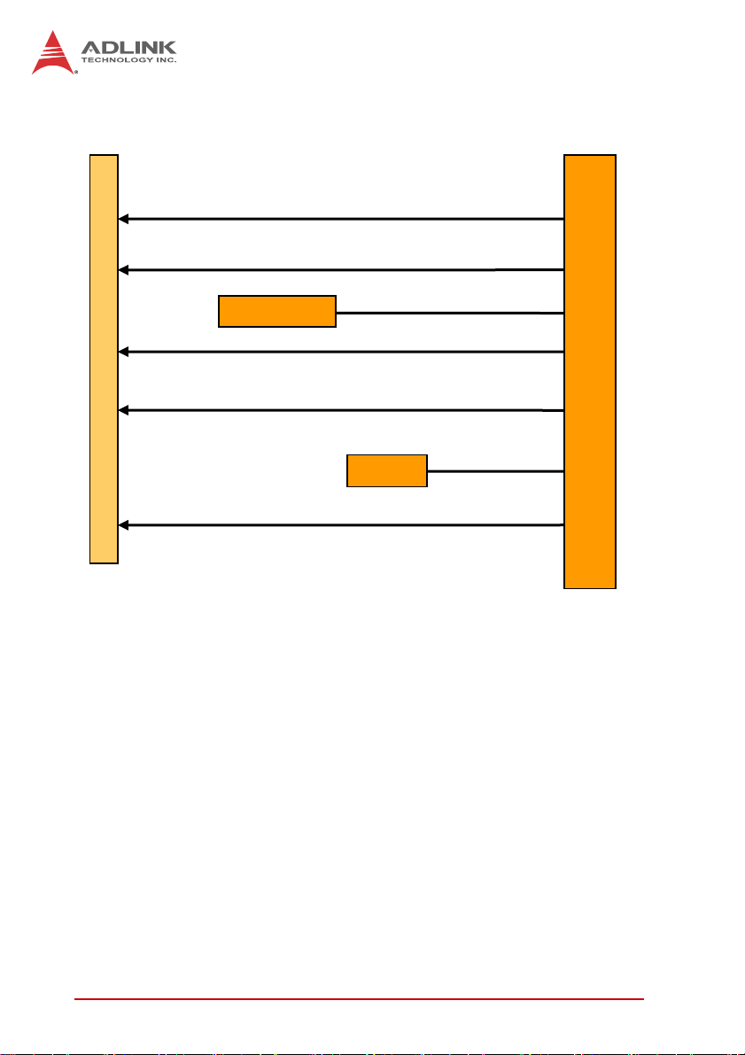
Figure 2-1: cPCI-3970 Blade Functional Block Diagram
*PCI Express to the J2 connector is set to PCIe x4 by default. If
you require 4x PCIe x1 at J2, please contact ADLINK for an
NOTE:
NOTE:
alternate BIOS version.
12 Specifications
DB-3610L2 Daughter Board
cPCI-3970
L2
F
R
O
N
T
P
A
N
E
L
PS/2, KB/MS
USB x2
Line-in, Line-out
2.5” HDD
COM
Codec
SATA0
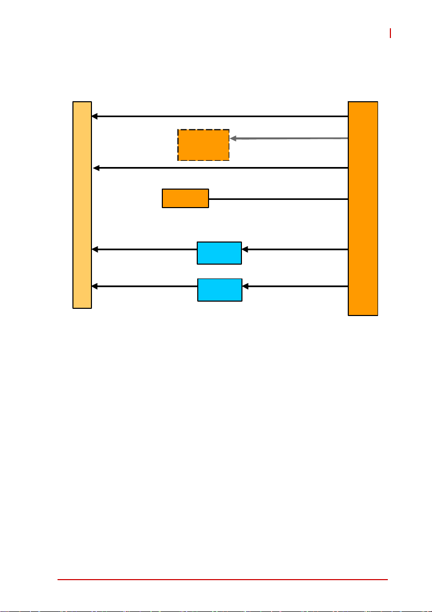
Figure 2-2: DB-3610L2 Daughter Board Functional Block Diagram
B2B
Conn.
1
Specifications 13
DB-3970L2 Daughter Board
L2
USB
F
R
O
DVI/DP
N
T
P
DVI/DP
A
N
E
L
2.5” HDD/SSD
10-pin
SATA0
COM1
COM2
KB/MS
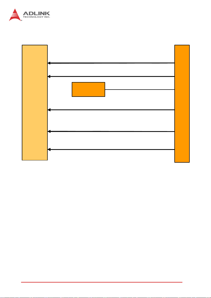
Figure 2-3: DB-3970L2 Daughter Board Functional Block Diagram
B2B
Conn.
1/2
14 Specifications
DB-LANL2-S Daughter Board
USB x1
L2
F
R
O
RS232/422/485
N
T
P
A
N
E
GbE 3
L
Horizontal
Type A
2.5” HDD
82574L
cPCI-3970
B2B
Conn.
USB x1
SATA0
GbE 4
82574L
Figure 2-4: DB-LANL2-S Daughter Board Functional Bl ock Diagram
Specifications 15
DB-Max Daughter Board
0
100-pin
high
density
connector
F
R
O
N
T
P
A
N
E
L
Line-in, Line-out
2x DVI/DP
2.5” HDD/Slim
SSD
2x USB 2.0
2x COM (RS232/422/485)
KB/MS
SATA
Figure 2-5: DB-Max Daught er Bo ard Functional Block Diagram
B2B
Conn.
16 Specifications
 Loading...