

Page 1
cPCI-3615 Series
3U CompactPCI® Dual-Core Intel® Atom™
Processor Blade
User’s Manual
Manual Rev.: 2.01
Revision Date: June 13, 2012
Part No: 50-15077-1010
Advance Technologies; Automate the World.
Page 2

Revision History
Revision Release Date Description of Change(s)
2.00 2011/04/29 Initial release
Correct Atom N455 frequency, board layout; add
2.01 2012/06/13
DB-3610CF removal instructions; correct J2 pin
def’n
Page 3

cPCI-3615
Preface
Copyright 2011-12 ADLINK Technology Inc.
This document contains proprietary infor mation protected by copyright. All rights are reserved. No part of this manual may be reproduced by any mechanical, electronic, or other means in any form
without prior written permission of the manufacturer.
Disclaimer
The information in this document is subject to change without prior
notice in order to improve reliability, design, and function and does
not represent a commitment on the part of the manufa cturer.
In no event will the manufacturer be liable for direct, indirect, special, incidental, or consequential damages arising out of the use or
inability to use the product or documentation, even if advised of
the possibility of such damages.
Environmental Responsibility
ADLINK is committed to fulfill its social responsibility to global
environmental preservation through compliance with the European Union's Restriction of Hazardous Substances (RoHS) directive and Waste Electrical and Electronic Equipment (WEEE)
directive. Environmental protection is a top priority for ADLINK.
We have enforced measures to ensure that our products, manufacturing processes, components, and raw materials have as little
impact on the environment as possible. When products are at their
end of life, our customers are encouraged to dispose of them in
accordance with the product disposal and/or recovery programs
prescribed by their nation or company.
Trademarks
Product names mentioned herein are used for identification purposes only and may be trademarks and/or registered trademarks
of their respective companies.
Preface iii
Page 4

Using this Manual
Audience and Scope
The cPCI-3615 User’s Manual is intended for hardware
technicians and systems operators with knowledge of installing,
configuring and operating CompactPCI systems.
Manual Organization
This manual is organized as follows:
Chapter 1, Introduction: Introduces the cPCI-3615, its features,
block diagrams, and package contents.
Chapter 2, Specifications: Presents detailed specification infor-
mation, power consumption, and technical drawings.
Chapter 3, Functional Description: Describes the cPCI-3615
main functions.
Chapter 4, Board Interfaces: Describes the cPCI-3615 board
interfaces.
Chapter 5, Getting Started: Describes the installation of compo-
nents to the cPCI-3615 and rear transition modules.
Chapter 6, Driver Installation: Provides information on how to
install the cPCI-3615 device drivers.
Chapter 7, Utilities: Describes the utilities of the cPCI-3615
Series.
Chapter 8, BIOS Setup: Describes basic navigation for the
AMIBIOS®8 BIOS setup utility.
Important Safety Instructions: Presents safety instructions all
users must follow for the proper setup, installation and usage of
equipment and/or software.
Getting Service: Contact information for ADLINK’s worldwide
offices.
iv Preface
Page 5
cPCI-3615
Conventions
Take note of the following conventions used throughout this
manual to make sure that users perform certain tasks and
instructions properly.
Additional information, aids, and tips that help users perform
tasks.
NOTE:
NOTE:
Information to prevent minor physical injury, component damage, data loss, and/or program corruption when trying to com-
CAUTION:
WARNING:
plete a task.
Information to prevent serious physical injury, component
damage, data loss, and/or program corruption when trying to
complete a specific task.
Preface v
Page 6

This page intentionally left blank.
vi Preface
Page 7

cPCI-3615
Table of Contents
Revision History...................................................................... ii
Preface.................................................................................... iii
List of Figures........................................................................ xi
List of Tables........................................................................ xiii
1 Introduction ........................................................................ 1
1.1 Overview.............................................................................. 1
1.2 Features............................................................................... 2
1.3 Block Diagram ..................................................................... 3
1.4 Product List............................. ... .......................................... 4
1.5 Package Contents ............................................................... 5
2 Specifications..................................................................... 7
2.1 cPCI-3615 Specifications........... ... ... .... ... ... ... ... .... ... ... ... .... ... 7
2.2 I/O Connectivity Table ......................................................... 9
2.3 Power Requirements.................... ... .... ... ... ... ... .... ... ... ... .... . 10
3 Functional Description .................................................... 13
3.1 Processor........................................................................... 13
3.2 Chipset............................................................................... 16
3.3 Super I/O ........................................................................... 16
3.4 Battery ............................................................................... 17
3.5 PMC/XMC.......................................................................... 17
4 Board Interfaces............................................................... 19
4.1 cPCI-3615 Blade Board Layout......................................... 19
4.2 cPCI-3615 Blade Assembly Layout ................................... 20
4.3 cPCI-3615D Blade Assembly Layout................................. 21
4.4 cPCI-3615P Blade Assembly Layout................................. 22
vii
Page 8

4.5 cPCI-3615 Series Front Panel Layout ............................... 23
4.6 cPCI-R3610T RTM Board Layout...................................... 25
4.7 cPCI-R3610(T) RTM Front Panel ...................................... 26
4.8 Connector Pin Assignments............................................... 27
4.9 Switch and Jumper Settings .............................................. 41
5 Getting Started.................................................................. 47
5.1 CPU and Heatsink ............................................................. 47
5.2 Hard Drive Installation........................................................ 48
5.3 PMC/XMC Card Installation............................................... 55
5.4 Removing the DB-3610CF Daughter Board ...................... 59
5.5 Installing the cPCI-3615 to the Chassis............................. 62
5.6 RTM Installation - cPCI-R3610(T)...................................... 63
6 Driver Installation.............................................................. 65
7 Utilities............................................................................... 67
7.1 Watchdog Timer................................................................. 67
7.2 Preboot Execution Environment (PXE).............................. 72
8 BIOS Setup........................................................................ 73
8.1 Starting the BIOS............................................................... 73
8.2 Main Setup......................................................................... 77
8.3 Advanced BIOS Setup....................................................... 77
8.3.1 CPU Configuration.........................................................79
8.3.2 IDE Configuration ..........................................................81
8.3.3 Super IO Configuration..................................................82
8.3.4 Hardware Health Configuration .....................................83
8.3.5 USB Configuration.........................................................84
8.3.6 AHCI Configuration.......................... .... ... ... ... ... ..............86
8.3.7 Remote Access Configuration .......................................87
8.4 Advanced PCI/PnP Settings.............................................. 89
viii
Page 9

cPCI-3615
8.5 Boot Settings ..................................................................... 90
8.5.1 Boot Settings Configuration............ ... ... ... ... .... ... ... ... .... .. 91
8.6 Security Setup ................................................................... 92
8.7 Chipset Setup.................................................................... 94
8.8 Exit Menu........................................................................... 95
Important Safety Instructions.............................................. 97
Getting Service...................................................................... 99
ix
Page 10

This page intentionally left blank.
x
Page 11

cPCI-3615
List of Figures
Figure 1-1: cPCI-3615 Series Functional Block Diagram...................3
Figure 4-1: cPCI-3615 Blade Board Layout.....................................19
Figure 4-2: cPCI-3615 Assembly Layout .........................................20
Figure 4-3: cPCI-3615D Board Layout.............................................21
Figure 4-4: cPCI-3615, cPCI-3615D Front Panel Layout................. 23
Figure 4-5: cPCI-3615P Front Panel Layout.................................... 24
Figure 4-6: cPCI-R3610T RTM Board Layout..................................25
Figure 4-7: cPCI-R3610(T) RTM Front Panel ..................................26
List of Figures xi
Page 12

This page intentionally left blank.
xii List of Figures
Page 13

cPCI-3615
List of Tables
Table 4-1: cPCI-3615 Front Panel System LED Descriptions ........ 24
Table 4-2: USB Connector Pin Definition........................................27
Table 4-3: VGA Connector Pin Definition.................... .... ... ... ... .... .. 27
Table 4-4: GbE Connector Pin Definitions...................................... 28
Table 4-5: Ethernet Status LED Definitions........... ... ... .... ... ... ... .... .. 28
Table 4-6: PS/2 Keyboard/Mouse Connector Pin Definition...........29
Table 4-7: DB-9 Serial Port Connector Pin Definition..................... 29
Table 4-8: cPCI-R3610(T) Serial Port Pin Header Definition..........30
Table 4-9: Serial ATA Connector on RTM Pin Definition................ 30
Table 4-10: Serial ATA Connector on DB-3610L2 Pin Definition......31
Table 4-11: CompactFlash Connector Pin Definition........................32
Table 4-12: DB-3610CF Connector Pin Definition............................33
Table 4-13: DB-3610L2 Connector Pin Definition............................. 34
Table 4-14: DB-3UMC Connector Pin Definition...............................35
Table 4-15: PMC Connector Pin Definitions..................................... 36
Table 4-16: XMC Connector Pin Definition.................... .... ... ... ... .... .. 38
Table 4-17: CompactPCI J1 Connector Pin Definition...................... 39
Table 4-18: CompactPCI J2 Connector Pin Definition...................... 40
Table 4-19: VGA/GPIO Mode Switch Settings.............. .... ... ... ... .... .. 41
Table 4-20: COM1 Mode Selection Switch Settings.........................42
Table 4-21: COM2 Mode Selection Switch Settings.........................43
Table 4-22: COM3 Mode Selection Switch Settings.........................44
Table 4-23: XMC VPWR Select Jumper Settings.............................45
Table 4-24: PMC V(I/O) Select Jumper Settings............................ .. 45
List of Tables xiii
Page 14

This page intentionally left blank.
xiv List of Tables
Page 15

1 Introduction
1.1 Overview
The cPCI-3615 Series is a 3U CompactPCI single board computer
in single-slot (4HP), dual-slot (8HP) or triple-slot (12HP) width
form factor featuring the Intel® Atom™ N455 or D525 processor
with ICH8M I/O Controller Hub. The cPCI-3615 provides single
channel DDR3-800 soldered onboard memory up to 4GB, integrated graphics on the CPU, IDE CompactFlash slot, and
2.5” SATA HDD (cPCI-3615D/P) and one PMC/XMC site
(cPCI-3615P). Front panel I/O includes 2x USB, 2x GbE, VGA,
and additional 2x USB, COM, KB/MS, and line-in/out for the
8(12)HP cPCI-3615D(P) models.
The optional Rear Transition Module (RTM) provides 2x SATA,
2x GbE, 1x USB, 2x COM, and VGA ports. One PCI-Express x1
port, GPIO and SMBus signals are routed to the J2 connector. The
cPCI-3615 Series is ideally suited for transportation, factory automation, and other industrial applications.
cPCI-3615
Introduction 1
Page 16

1.2 Features
X 3U CompactPCI blade in 4HP, 8HP or 12HP width form factor
X Supports Dual-Core or Single-Core Intel® Atom™ processor,
up to 1.8 GHz
X Graphics and memory controllers integrated in processor
X ICH8M I/O Hub
X Single channel DDR3-800 SDRAM soldered onboard, up to
4GB
X 32bit/33MHz CompactPCI Interface based on PCI specifica-
tions
X Optional 32bit/66MHz PMC or PCI-Express x1 XMC site
X VGA port on front or switchable to RTM
X Two PCI-Express® Gigabit Eth ernet egress ports , configurable
to RTM by software
X One IDE CompactFlash socket
X Line-in and Line-out ports on front panel
X 2.5” SATA HDD onboard on 8HP/12HP blade and two 7-pin
SATA ports on RTM
2Introduction
Page 17
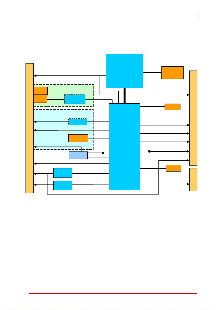
1.3 Block Diagram
C
RGB
Intel® Atom™
Processor
N455/D525
DDR3-800
cPCI-3615
Soldered
Up to 4GB
XMC
PMC
F
R
O
N
Line-in, Line-out
T
USB 3/4
P
A
N
E
COM1, KB/MS
L
USB 1/2
GbE 2
GbE 1
DB-3UMC
32b/66M
I
P
PCIe x1
PCIe-to-PCI
Bridge
PCIe x1
DMI
IDE
DB-3610L2
HD
SATA 1
COM2/3
LPC
Intel®
ICH8M
PCIe x1, GPIO, SMBus
SATA 2/3
1x USB
COM2,COM3
GbE 1/2
SPI
PCI 32b/33M
Intel
82574L
Intel
82574L
Codec
2.5” HDD
IT8783F
PCIe x1
PCIe x1
Figure 1-1: cPCI-3615 Series Functional Block Diagram
RGB
CF
J2
BIOS
J1
Introduction 3
Page 18

1.4 Product List
Products in the cPCI-3615 Series include:
Processor Blade
X cPCI-3615: 4HP width (single-slot) 3U CompactPCI featur-
ing Atom™ N455 or D525 processor; 1GB, 2GB or 4GB
memory soldered onboard; CompactFlash slot; 2x USB;
2x GbE; VGA.
X cPCI-3615D: 8HP width (dual-slot) 3U CompactPCI featur-
ing Atom™ N455 or D525 processor; 1GB, 2GB or 4GB
memory soldered onboard; CompactFlash slot; 2x USB; 2x
GbE; VGA. The DB-3610L2 riser card onboard provides 2x
USB, COM, PS/2 KB/MS, Line-in, Line-out ports.
X cPCI-3615P: 12HP width (triple-slot) 3U CompactPCI fea-
turing Atom™ N455 or D525 processor; 1GB, 2GB or 4GB
memory soldered onboard; CompactFlash slot; 2x USB; 2x
GbE; VGA. The DB-3610L2 riser card onboard on the 2nd
layer provides 2x USB, COM, PS/2 KB/MS, Line-in,
Line-out ports. The DB-3UMC riser card on the 3r d layer
provides one PMC/XMC site.
X Extended Temperature: -20°C to 70°C operating tempera-
ture range is supported by the cPCI-ET3615,
cPCI-ET3615D and cPCI-ET3615P
X Extreme Temperature: -40°C to 85°C operating tempera-
ture range is supported by the cPCI-EX3615,
cPCI-EX3615D and cPCI-EX3615P
Rear Transition Module
X cPCI-R3610: 8HP width, 50mm depth Rear Transition Mod-
ule with 2x COM, USB, 2x GbE, 2x SATA, VGA
X cPCI-R3610T: 8HP width, 80mm depth Rear Transition
Module with 2x COM, USB, 2x GbE, 2x SATA, VGA
4Introduction
Page 19

cPCI-3615
1.5 Package Contents
The cPCI-3615 is packaged with the following components. If any
of the items on the contents list are missing or damaged, retain the
shipping carton and packing material and contact the dealer for
inspection. Please obtain authorization before returning any product to ADLINK. The packing contents of the cPCI-3615 Series are
non-standard configurations and may vary depending on customer
requests.
Processor Blade
X The cPCI-3615 Series Processor Blade
Z CPU, RAM specifications will differ depending on
options selected
Z Thermal module is assembled on the board
X Y-cable for PS/2 combo port (8HP/12HP version only)
X 2.5” HDD accessory pack (8HP/12HP version only)
X ADLINK All-in-One CD
X User’s manual
Rear Transition Module
X cPCI-R3610: 8HP width, 50mm depth Rear Transition Mod-
ule with 2x COM, USB, 2x GbE, 2x SATA, VGA
X cPCI-R3610T: 8HP width, 80mm depth Rear Transition
Module with 2x COM, USB, 2x GbE, 2x SATA, VGA
The contents of non-standard cPCI-3615 configurations may
vary depending on the customer’s requirements.
NOTE:
NOTE:
This product must be protected from static discharge and physical shock. Never remove any of the components except at a
CAUTION:
static-free workstation. Use the anti-static bag shipped with the
product when putting the board on a surface. Wear an
anti-static wrist strap properly grounded on one of the system's
ESD ground jacks when installing or servicing system components.
Introduction 5
Page 20

This page intentionally left blank.
6Introduction
Page 21

2 Specifications
2.1 cPCI-3615 Specifications
cPCI-3615
CompactPCI®
Standards
Mechanical • Standard 3U CompactPCI®
Processor • µFC-BGA Intel® Atom™ Processor N455
Chipset • Intel® ICH8M I/O Controller Hub (ICH)
Memory
BIOS • AMIBIOS8® 16Mbit SPI flash memory
CompactPCI
Bus
Gigabit
Ethernet
Graphics • In te grated in Intel® Atom™ Processor
Serial Ports • Up to three 16C550 compatible RS-232/422/485/485+
Storage
Interface
PMC/XMC • On e 32bit/66MHz PMC or PCI-Express x1 XMC site
Audio • Line-in and Line-out ports on front panel (8HP/12HP only)
BIOS • AMIBIOS8® 16Mbit SPI flash memory
1
• P ICMG® 2.0 CompactPCI® Rev. 3.0
• P ICMG® 2.1 Hot Swap Specification Rev.2.0
• B oard size: 100mm x 160mm
• Single-slot (4HP, 20.32mm); Dual-slot (8HP, 40.64mm),
Triple-slot (12HP, 60.96mm) width
• CompactPCI® connectors with J1, J2
1.66 GHz, 512KB L2 cache, TDP 6.5W
• µFC-BGA dual-core Intel® Atom™ Processor D525
1.8 GHz, 1MB L2 cache, TDP 13W
• Passive heatsink
• Single channel unbuffered DDR3-800 SDRAM soldered
onboard
• Up to 2GB for N455 processor, 4GB for D525 processor
• PCI 32bit/ 33MHz; 3.3V, 5V universal V(I/O)
• Supports operation in system slot only
• Two PCI-Express x1 Intel® 82574L GbE controllers
• Two egress 10/100/1000BASE-T ports, configurable to J2
(RTM) by software setting
• DB-15 VGA port on front panel, switchable to J2 (RTM)
• Analog monitor support up to QXGA 2048x1536 @60Hz
32-bit
serial ports from Super I/O IT8783
• One DB-9 port on front panel, two DB-9 ports on rear panel
• CompactFlash Type II socket onboard
• 2.5” SAT A HDD connector onboard
• Two 7-pin SATA signal connectors on RTM
(12HP version only)
• Realtek ALC262 High Definition Audio Codec
(8HP/12HP version only)
Specifications 7
Page 22

Faceplate I/O
4HP (cPCI-3615):
• 2x USB 2.0 ports
• 2x 10/100/10 00BASE-T Ethernet ports
• Analog DB-15 VGA port
8HP (cPCI-3615D):
• 4x USB 2.0 ports
• 2x 10/100/10 00BASE-T Ethernet ports
• Analog DB-15 VGA port
• DB-9 RS-232/422/485/485+ port
• PS/2 Keyboard/ Mouse combo port
• Line-in and Line-out ports
cPCI-R3610(T):
• 2x USB 2.0 ports
• 10/100/1000BASE-T Ethernet port
• 2x DB-9 RS-232 serial ports
OS
Compatibility
• Mi crosoft Windows XP Professional, x64 Editio n
• Mi crosoft Windows Vista x64 Edition
• Mi crosoft Windows 7 x86 Edition
• Red Hat Enterprise Linux 5.3
• Fedora 12
• Other OS supp ort upon request
Environmental • Operating Temperature (with forced air flow)2:
- Standard: 0°C to 60°C
- Extended: -20°C to 70°C
- Extreme Extended temperature: -40°C to 85°C
• Storage Temperature: -40°C to 85°C
• Humidity: 90% @ 60°C non-condensing
• Shock: 15G peak-to-peak, 11ms duration, non-operating
•Vibration1: Operating 1.88Grms, 5-500Hz, each axis w/o HDD
EMI • CE EN55022
• FCC Cla ss A
Specifications are subject to change without prior notice.
1. Hard drive limits operational vibration. When application requires
higher vibration specification, it is recommended to use a flash disk.
2. ADLINK-certified thermal design. The thermal performance is
dependent on the chassis cooling design. Forced airflow with
3.2 m/s is required. Temperature limit of optional mass storage
devices may affect the thermal specification.
8 Specifications
Page 23

2.2 I/O Connectivity Table
cPCI-3615
Function
Gigabit
Ethernet
COM
USB 2.0
VGA
Serial
ATA
CF
PS/2
KB/MS
Line-in
Line-out
PMC/
XMC
GP LED
Reset
Btn.
cPCI-3615
(4HP)
Front I/O Onboard Front I/O Onboard Front I/O Onboard Front I/O Onboard
Y x2 – Y x2 – Y x2 –
–Y–Y–Y x2–
Y x2 – Y x4 – Y x4 – Y –
Y– Y – Y –
–– –
–Y – Y – Y – –
––Y–Y–––
––Y–Y–––
––Y–Y–––
–– – – –Y– –
Y x2 – Y x2 – Y x2 – – –
Y–Y–Y–––
cPCI-3615D
(8HP)
(2.5” HD)
cPCI-3615P
(12HP)
Y
–
Y
(2.5” HD)
cPCI-R3610(T)
Y x2
Y
(1)
(1)
–
–
–
Yx2
(7-pin)
1. Software switchable from front port(s).
Specifications 9
Page 24
2.3 Power Requirements
In order to guarantee stable operation of the system, it is recommended that significantly more power be provided than required.
An industrial power supply unit should be able to provide at
least twice as much power as the entire system requires of
each voltage. An ATX power supply unit should be able to provide
at least three times as much po wer as the entire syst em requires
of each voltage.
The tolerance of the voltage lines described in the CompactPCI
specification (PICMG 2.0 R3.0) is +5%/-3% for 5, 3.3 V and ±5%
for ±12V. This specification is for power delivered to each slot and
it includes both the power supply and the backplane tolerance.
Voltage
5V +5.0 VDC +5% / -3% 50 mV
3.3V +3.3 VDC +5% / -3% 50 mV
+12V +12 VDC +5% / -5% 240 mV
-12V -12 VDC +5% / -5% 240 mV
V I/O (PCI I/O
Buffer Voltage)
GND
Nominal
Value
+3.3 VDC or
+5 VDC
Tolerance
+5% / -3% 50 mV
Max. Ripple
(P - P)
10 Specifications
Page 25

cPCI-3615
Power Consumption
This section provides information on the power consumption of
cPCI-3615 Series when using Intel® Atom™ processors with 1GB
soldered DDR2 memory and onboard 80GB SATA hard drive. The
cPCI-3615 is powered by 5V only. Power consumption at 100%
CPU usage was measured using PassMark BurnInTest 6.0.
Intel® Atom™ Processor N455
OS/Mode Current 5V Total Power
DOS/Idle mode 2.94A 14.7W
Linux/Idle mode 2.54A 12.7W
Windows XP/
Idle mode
Windows® XP,
100% CPU Usage
Intel® Atom™ Processor D525
OS/Mode Current 5V Total Power
DOS/Idle mode 2.99A 14.9W
Linux/Idle mode 2.79A 13.9W
Windows XP/
Idle mode
Windows® XP,
100% CPU Usage
2.95A 14.7W
3.02A 15.1W
3.04A 15.2W
3.48A 17.4W
Specifications 11
Page 26

This page intentionally left blank.
12 Specifications
Page 27

3 Functional Description
The following sections describe the cPCI-3615 Series features
and functions.
3.1 Processor
cPCI-3615
The cPCI-3615 Series supports the
Intel® Atom™ Processor N400,
D400 and D500 Series processors built on 45-nm Hi-K process
technology. The processor is designed for a two-chip platform as
opposed to the traditional three-chip platforms (processor, GMCH,
and ICH). The two-chip platform consists of a processor and the
chipset and enables higher performance, lower cost, easier validation, and improved x-y footprint.
Features Atom™N455 Atom™D525
Clock 1.66 GHz 1.8 GHz
L2 cache 512KB 1MB
No. of Core(s) 1 2
Max. Power (TDP1)
T
junction, MAX
1. The high est expected sustainable power while running known
power intensive applications. TDP is not the maximum power
that the processor can dissipate.
2. The maximum supported operating temperature.
2
6.5W 13W
100°C 100°C
Intel® Atom™ Processor N455
Included in this family of processors is an integrated memory controller, integrated graphics processing unit and integrated I/O
(such as DMI) on a single silicon die.
The following list outlines the key features of this processor:
X One die, primary 32-kB instructions cache and 24-kB
write-back data cache
X Intel® Hyper-Threading Technology (2 threa ds)
X On die 512-kB, 8-way L2 cache
X Support IA 32-bit and Intel® 64 architecture
X Intel® SSE2 and SSE3 and SSSE3 support
Functional Description 13
Page 28

X Micro-FCBGA8 packaging technologies
X Thermal management support via Intel® Thermal Monitor 1
(TM1) and Intel® Thermal Monitor 2 (TM2)
X Enhanced Intel® SpeedStep Technology (EIST)
X Support L2 dynamic cache sizing
The following list outlines the key features of system memory support:
X One channel DDR3 memory
X Memory DDR3 data transfer rates of 800 MT/s
X Non-ECC, unbuffered DDR3
X 512Mb. 1-Gb,and 2-Gb DDR3 DRAM technologies supported
X Maximum of 2-GB memory capacity supported
X Maximum 2GB memory capacity on one SO-DIMM or Mem-
ory Down
The following list outlines the key graphics features:
X The integrated graphics controller contains a refresh of the
3rd generation graphics core
X Intel® Dynamic Video Memory Technology 4.0
X Directx* 9 compliant Pixel Shader v2.0
X 200-MHz render clock frequency
X Analog RGB display output up to resolution up to
1400x1050 @ 60Hz
Intel® Atom™ Processor D525
The following list provides some of the key features of this processor:
X One die, primary 32-kB instructions cache and 24-k B
write-back data cache
X Intel® Hyper-Threading Technology (2 threads per core)
X On die 2x512-kB, 8-way L2 cache
X Support IA 32-bit and Intel® 64 architecture
X Intel® SSE2 and SSE3 and SSSE3 support
X Micro-FCBGA8 packaging technologies
X Thermal management support via Intel® Thermal Monitor 1
(TM1)
14 Functional Description
Page 29

cPCI-3615
The following list outlines the key features of system memory support:
X One channel DDR3 memory
X Memory DDR3 data transfer rates of 800 MT/s
X Non-ECC, unbuffered DDR3
X I/O Voltage of 1.8V for DDR3
X 512Mb. 1-Gb,and 2-Gb DDR3 DRAM technologies supported
The following list outlines the key graphics features:
X The integrated graphics controller contains a refresh of the
3rd generation graphics core
X Intel® Dynamic Video Memory Technology 4.0
X Directx* 9 compliant Pixel Shader v2.0
X 400-MHz render clock frequency
X Analog RGB display output up to resolution up to
2048x1536 @ 60Hz
Functional Description 15
Page 30

3.2 Chipset
Intel® ICH8 Mobile I/O Controller Hub
The ICH8M provides extensive I/O support. Functions and capabilities include:
X Provides 6 PCI Expressx1 ports, supporting the PCI
Express Base Specification, Revision 1.1. Each Root Port
supports 2.5GB/s bandwidth in each direction. The
cPCI-3615 utilizes two PCI Express x1 ports for two Gigabit
Ethernet controllers; routes two PCI Express x1 ports to the
board-to-board connector and one PCI Express x1 port to
the J2 connector for expansion capability.
X Enhanced DMA controller, interrupt controller, and timer functions
X Integrated Serial A TA host controller with independent DMA
operation on three ports
X Integrated IDE controller supports Ultra ATA100/66/33
X System Management Bus (SMBus) Specification, Version
2.0 with additional support for I2C devices
X Supports Intel® Matrix Storage Technology
X PCI Local Bus Specification, Revision 2.3 support for
33MHz PCI operations
3.3 Super I/O
The ITE IT8783F Super I/O is on a Low Pin Count interface supporting PS/2 keyboard/mouse; three 16C550-compatible serial
ports; hardware monitor function to monitor CPU voltage, CPU
temperature, power supply voltages and system temperature; and
Watchdog Timer with time resolution from minimum 1 second or
minute to maximum 65635 seconds or minutes on the cPCI-3615.
16 Functional Description
Page 31

cPCI-3615
3.4 Battery
The cPCI-3615 is provided with a 3.0V “coin cell” lithiu m battery
for the Real Time Clock (RTC). The battery socket is equipped on
the DB-3610CF daughter board. The lithium battery must be
replaced with an identical battery or a battery type recommended
by the manufacturer. The cPCI-3615 is equipped with a Rayovac
BR2032 by default, and can be optionally equipped with a Gold
Capacitor.
3.5 PMC/XMC
The cPCI-3615P Series supports one PMC or XMC site for front
panel I/O expansion. The PMC site provides a maximum 32bit/
66MHz PCI bus link using a Pericom PI7C9X110
PCI-Express-to-PCI bridge and PCI-Express x1 link. The PMC site
supports +3.3V and +5V signaling. The XMC site provides a PCI
Express x1 port.
Functional Description 17
Page 32

This page intentionally left blank.
18 Functional Description
Page 33

4 Board Interfaces
This chapter illustrates the board layout, connector pin
assignments, and jumper settings to familiarize users with the
cPCI-3615 Series.
4.1 cPCI-3615 Blade Board Layout
cPCI-3615
LAN
VGA
USB0
USB1
CPU Intel® Atom processor USB0/1 USB 2.0
SB South Bridge Intel® ICH8M CN4 DB-3610L2 connector
LAN GbE Controller Intel® 82574L CN2 DB-3610CF connector
RAM DDR2 SDRAM SW1 VGA/GPIO Mode Switch
CN1 Dual RJ-45 GbE ports
CN2 VGA connector CompactPCI connectors
LAN
LAN
CN4
Figure 4-1: cPCI-3615 Blade Board Layout
RAM
CPU
SB
(SW3 on solder side)
CN2
SW1
J2
J1
Board Interfaces 19
Page 34

4.2 cPCI-3615 Blade Assembly Layout
This section describes the final as sembly layout of the single slot
cPCI-3615 (4HP).
DB-3610CF
Battery
Heat sink
CF socket
Figure 4-2: cPCI-3615 Assembly Layout
20 Board Interfaces
Page 35

cPCI-3615
4.3 cPCI-3615D Blade Assembly Layout
The dual-slot width cPCI-3615D (8HP) is comprised of the
cPCI-3615 single-slot main board and the DB-36 10L2 r i ser ca rd to
expand I/O connectivity with PS/2, COM, 2x USB, Line-in, and
Line-out ports.
DB-3610L2
COM1
USB2
USB3
PS2
SATA0
2.5” SATA HDD
CN6
CN8
CN7
COM1 DB-9 COM port CN7 DB-3UMC connector
USB2/3 USB connectors CN6 Line-in port
PS2 PS/2 KB/MS combo port CN8 Line-out port
SATA0 22-pin SATA connector
Figure 4-3: cPCI-3615D Board Layout
Board Interfaces 21
Page 36

4.4 cPCI-3615P Blade Assembly Layout
The triple-slot width cPCI-3615P (12HP) is comprised of the
cPCI-3615D dual-slot assembly and the DB-3UMC riser card to
provide a PMC/XMC slot for front I/O expansion.
JN3
JN1
JN2
DB-3UMC
DB-3UMC
JN1/2 PMC connectors JN3 XMC connector
22 Board Interfaces
Page 37

4.5 cPCI-3615 Series Front Panel Layout
cPCI-3615
cPCI-3615
WDT LED
Reset button
cPCI-3615D
WDT LED
Reset button
GbE 1/2
12
Power LED
COM1
12
Power LED
USB 2.0
VGA
PS/2
KB/MS
VGA
USB 2.0
Line-in
Line-out
USB 2.0
Figure 4-4: cPCI-3615, cPCI-3615D Front Panel Layout
Board Interfaces 23
Page 38

cPCI-3615P
COM1
USB 2.0
PS/2
KB/MS
Line-in
Line-out
PMC/XMC
WDT LED
VGA
Reset button
Power LED
USB 2.0
Figure 4-5: cPCI-3615P Front Panel Layout
Optional 2-slot version with PMC/XMC as shown below is avail-
able by request. Please contact your ADLINK sales representative.
PMC/XMC
System LEDs
LED Color Condition Indication
Power Green
WDT Red
OFF System is off
ON System is on
OFF No Watchdog event
Blinking Watchdog event alert
Table 4-1: cPCI-3615 Front Panel System LED Descriptions
24 Board Interfaces
Page 39

4.6 cPCI-R3610T RTM Board Layout
SATA1
SATA2
cPCI-3615
rJ2
LAN
COM2
SW1-4
COM3
USB 5
VGA1
SW5-8
COM2/3 COM ports LAN Dual Ethernet port
SATA1/2 SATA ports USB5 USB port
rJ2 CompactPCI connector SW1-8 Switches
VGA1 VGA connector
Figure 4-6: cPCI-R3610T RTM Board Layout
Board Interfaces 25
Page 40

4.7 cPCI-R3610(T) RTM Front Panel
COM3
VGA
Figure 4-7: cPCI-R3610(T) RTM Front Panel
COM2
12
USB GbE x2
26 Board Interfaces
Page 41

4.8 Connector Pin Assignments
USB Connectors
Pin # Signal Name
1Vcc
2UV03UV0+
4GND
Table 4-2: USB Connector Pin Definition
VGA Connector (DB-15)
Signal Name Pin # Pin # Signal Name
Red 1 2 Green
Blue 3 4 N.C.
GND 5 6 GND
GND 7 8 GND
+5V. 9 10 GND
N.C. 11 12 CRTDATA
HSYNC 13 14 VSYNC
CRTCLK 15
cPCI-3615
Table 4-3: VGA Connector Pin Definition
Board Interfaces 27
Page 42

Gigabit Ethernet Connectors (RJ-45)
Pin #
1 TX+ BI_DA+
2 TX- BI_DA3 RX+ BI_DB+
4— BI_DC+
5 — BI_DC6 RX- BI_DB7— BI_DD+
8 — BI_DD-
Ta ble 4-4: GbE Connector Pin Definitions
Status
Network link is not established
or system powered off
10 Mbps
100 Mbps
1000 Mbps
10BASE-T/
100BASE-TX
Link OFF ON
Active OFF Blinking
Link Green ON
Active Green Blinking
Link Amber ON
Active Amber Blinking
1000BASE-T
81
Speed LED
(Green/Amber)
OFF OFF
Activity LED
(Yellow)
Ta ble 4-5: Ethernet Status LED Definitio ns
28 Board Interfaces
Page 43

PS/2 Keyboard/Mouse Connector
Pin # Signal Function
1 KBDATA Keyboard Data
2MSDATA Mouse Data
3 GND Ground
4+5V Power
5 KBCLK Keyboard Clock
6 MSCLK Mouse Clock
T able 4-6: PS/2 Keyboard/Mouse Connector Pin Definition
Serial Port DB-9 Connector (COM1)
Pin # RS-232 RS-422 RS-485(+)
1 DCD-L TXD- TXD2RXDTXD+TXD+
3TXDRXD+ —
4 DTR-L RXD- —
5 GND GND GND
6DSR-L — —
7RTS-L — —
8CTS-L — —
9RI-L — —
cPCI-3615
Table 4-7: DB-9 Serial Port Connector Pin Definition
Board Interfaces 29
Page 44

cPCI-R3610(T) Serial Port Pin Header (COM2/3)
Pin # RS-232 RS-422 RS-485(+)
1 DCD-L TXD- TXD2DSR-L — —
3 RXD TXD+ TXD+
12
4RTS-L — —
5 TXD RXD+ —
6CTS-L — —
910
7 DTR-L RXD- —
8RI-L — —
9GNDGNDGND
10———
Table 4-8: cPCI-R3610(T) Serial Port Pin Header Definition
Serial ATA Connectors on RTM
Pin # Signal
1GND
2TX+
3TX4GND
5RX6RX+
7GND
Table 4-9: Serial ATA Connector on RTM Pin Definition
1
7
30 Board Interfaces
Page 45

Serial ATA Connector on DB-3610L2
Pin # Signal
S1 GND
S2 TX+
S3 TXS4 GND
S5 RXS6 RX+
S7 GND
P1 NC
P2 NC
P3 NC
P4 GND
P5 GND
P6 GND
P7 5V
P8 5V
P9 5V
P10 GND
P11 NC
P12 GND
P13~P15 NC
cPCI-3615
S1
Signal
S7
P1
Power
P15
Table 4-10: Serial ATA Connector on DB-3610L2 Pin Definition
Board Interfaces 31
Page 46

CompactFlash Connector on DB-3610CF
Signal Name Pin# Pin# Signal Name
GND 1 26 GND
DD3 2 27 DD11
DD4 3 28 DD12
DD5 4 29 DD13
DD6 5 30 DD14
DD7 6 31 DD15
CS1J 7 32 CS3J
GND 8 33 GND
GND 9 34 SDIORJ
GND 10 35 SDIOWJ
GND 11 36 5V
GND 12 37 IRQ15
5V 13 38 5V
GND 14 39 PCSEL
GND 15 40 NC
GND 16 41 BRSTDRVJ
GND 17 42 SDIORDY
DA2 18 43 NC
DA1 19 44 SDACKJ
DA0 20 45 IDEACTJ
DD0 21 46 DIAG
DD12247DD8
DD22348DD9
IOIS16J 24 49 DD10
GND 25 50 GND
Table 4-11: CompactFlash Connector Pin Definition
32 Board Interfaces
Page 47

DB-3610CF Connector (CN2)
cPCI-3615
Signal Name Pin # Pin # Signal Name
IDE_D7 1 2 IDE_D8
IDE_D6 3 4 IDE_D9
IDE_D5 5 6 IDE_D10
IDE_D4 7 8 IDE_D11
IDE_D3 9 10 IDE_D12
IDE_D2 11 12 IDE_D13
IDE_D1 13 14 IDE_D14
IDE_D0 15 16 IDE_D15
GND 17 18 GND
IDE_REQ-L 19 20 IDE_66DECT
IDE_IOW-L 21 22 IDE_RST-L
IDE_IOR-L 23 24 SPKR
IDE_IORDY 25 26 SIO_SPKR
IDE_ACK-L 27 28 GND
IDE_IRQ 29 30 VCC_RTC
IDE_A1 31 32 GND
IDE_A0 33 34 USB4-P
IDE_A2 35 36 USB4-N
IDE_CS1-L 37 38 P5V
IDE_CS3-L 39 40 P5V
40 39
2
1
Table 4-12: DB-3610CF Connector Pin Definition
Board Interfaces 33
Page 48

DB-3610L2 Connector (CN4)
Signal Name Pin # Pin # Signal Name
USB2-N 1 2 -12V
USB2-P 3 4 +12
GND 5 6 GND
USB3-N 7 8 HDA_SDIN0
USB3-P 9 10 HDA_R_SDOUT
GND 11 12 GND
SATA_ICH_RX-N0 13 14 HDA_R_SYNC
SATA_ICH_RX-P0 15 16 HDA_R_BIT_CLK
GND 17 18 GND
SATA_TX-P0 19 20 CK_L2_PCIE1-P
SATA_TX-N0 21 22 CK_L2_PCIE1-N
GND 23 24 GND
PCIE_TXN5 25 26 CK_L2_PCIE2-P
PCIE_TXP5 27 28 CK_L2_PCIE2-N
GND 29 30 GND
PCIE_RXN5 31 32 HDA_R_RST-L
PCIE_RXP5 33 34 SPKR
GND 35 36 L2_PCIE_RST-L
PCIE_RXN4 37 38 NC
PCIE_RXP4 39 40 USB_2_3_OC-L
GND 41 42 COM1_DCD-L
PCIE_TXN4 43 44 COM1_RI-L
PCIE_TXP4 45 46 COM1_CTS-L
GND 47 48 COM1_DTR-L
MSCLK 49 50 COM1_RTS-L
MSDATA 51 52 COM1_DSR-L
KBCLK 53 54 COM1_SOUT
KBCDATA 55 56 COM1_SIN
P5V 57 58 +3.3V
P5V 59 60 +3.3V
60
12
59
Table 4-13: DB-3610L2 Connector Pin Definition
34 Board Interfaces
Page 49

DB-3UMC Connector (CN7)
Signal Name Pin # Pin # Signal Name
NC 1 2 -12V
NC 3 4 +12V
GND 5 6 GND
NC 7 8 NC
NC 9 10 NC
GND 11 12 GND
NC 13 14 NC
NC 15 16 NC
GND 17 18 GND
NC 19 20 CK_PCIE1_P
NC 21 22 CK_PCIE1_N
GND 23 24 GND
PCIE_TXN2 25 26 CK_PCIE2_P
PCIE_TXP2 27 28 CK_PCIE2_N
GND 29 30 GND
PCIE_R_RXN2 31 32 NC
PCIE_R_RXP2 33 34 NC
GND 35 36 PCIE_RST#
PCIE_R_RXN1 37 38 NC
PCIE_R_RXP1 39 40 NC
GND 41 42 NC
PCIE_TXN4 43 44 NC
PCIE_TXP4 45 46 NC
GND 47 48 NC
NC 49 50 NC
NC 51 52 NC
NC 53 54 NC
NC 55 56 NC
+5V 57 58 +3.3V
+5V 59 60 +3.3V
cPCI-3615
60
12
59
Table 4-14: DB-3UMC Connector Pin Definition
Board Interfaces 35
Page 50

PMC Connector (JN1/2)
Pin# JN1 Signal JN2 Signal
1 PMC_TCK P12V
2 N12V PMC_TRST-L
3 GND PMC_TMS
4 PCIX_INTA-L NC (PMC_TDO)
5 PCIX_INTB-L PMC_TDI
6PCIX_INTC-L GND
7PMC_MOD-L1 GND
8P5V NC
9PCIX_INTD-L NC
10 NC NC
11 GND PMC_MOD-L2
12 P3V3_PMCAUX P3V3
13 CLK66_PCIX_PMC PMC_RST-L
14 GND PMC_MOD-L3
15 GND P3V3
16 PCIX_GNT-L0 PMC_MOD-L4
17 PCIX_REQ-L0 PMC_PME-L
18 P5V GND
19 PMC_VIO PCIX_AD30
20 PCIX_AD31 PCIX_AD29
21 PCIX_AD28 GND
22 PCIX_AD27 PCIX_AD26
23 PCIX_AD25 PCIX_AD24
24 GND PCIX_AD23
25 GND PMC_IDSEL
26 PCIX_CBE-L3 PCIX_AD23
27 PCIX_AD22 P3V3
28 PCIX_AD21 PCIX_AD20
29 PCIX_AD19 PCIX_AD18
30 P5V GND
31 PCIX_FRAME-L PCIX_AD16
32 PCIX_AD17 PCIX_CBE-L2
6364
12
Table 4-15: PMC Connector Pin Definitions
36 Board Interfaces
Page 51

Pin# JN1 Signal JN2 Signal
33 PCIX_FRAME-L GND
34 GND NC
35 GND PCIX_TRDY-L
36 PCIX_IRDY-L P3V3
37 PCIX_DEVSEL-L GND
38 P5V PCIX_STOP-L
39 PCIX_PCIXCAP PCIX_PERR-L
40 PCIX_LOCK-L GND
41 NC P3V3
42 NC PCIX_SERR-L
43 PCIX_PAR PCIX_CBE-L1
44 GND GND
45 PMC_VIO PCIX_AD14
46 PCIX_AD15 PCIX_AD13
47 PCIX_AD12 PCIX_M66EN
48 PCIX_AD11 PCIX_AD10
49 PCIX_AD9 PCIX_AD8
50 P5V P3V3
51 GND PCIX_AD7
52 PCIX_CBE-L0 NC
53 PCIX_AD6 P3V3
54 PCIX_AD5 NC
55 PCIX_AD4 NC
56 GND GND
57 PMC_VIO NC
58 PCIX_AD3 NC
59 PCIX_AD2 GND
60 PCIX_AD1 NC
61 PCIX_AD0 PCIX_ACK64-L
62 P5V P3V3
63 GND GND
64 PCIX_REQ64-L NC
Table 4-15: PMC Connector Pin Definitions (cont’d)
cPCI-3615
Board Interfaces 37
Page 52

XMC Connector (JN3)
Pin# A B C D E F
1 RXP RXN 3.3V NC NC VPWR
2 GND GND Not used GND GND PCIE_RST-L
3 NC NC 3.3V NC NC VPWR
4 GND GND Not used GND GND Not used
5 NC NC 3.3V NC NC VPWR
6 GND GND Not used GND GND +12V
7 NC NC 3.3V NC NC VPWR
8 GND GND Not used GND GND -12V
9 NC NC Not used NC NC VPWR
10 GND GND Not used GND GND GA0
11 TXP TXN Not used NC NC VPWR
12 GND GND GA1 GND GND Not used
13 NC NC 3.3V NC NC VPWR
14 GND GND GA2 GND GND Not used
15 NC NC Not used NC NC VPWR
16 GND GND Not used GND GND Not used
17 NC NC Not used NC NC NC
18 GND GND Not used GND GND Not used
19 CK-P CK-N Not used Not used Not used Not used
Table 4-16: XMC Connector Pin Definition
38 Board Interfaces
Page 53

cPCI-3615
CompactPCI J1 Connector
Pin Z A B C D E F
25 GND +5V REQ64# ENUM# +3.3V +5V GND
24 GND CPCI_AD1 +5V CPCI_VIO CPCI_AD0 ACK64# GND
23 GND P3V3 CPCI_AD4 CPCI_AD3 P5V CPCI_AD2 GND
22 GND CPCI_AD7 GND P3V3 CPCI_AD6 CPCI_AD5 GND
21 GND P3V3 CPCI_AD9 CPCI_AD8 CPCI_M66EN CPCI_CBE-L0 GND
20 GND CPCI_AD12 GND VIO CPCI_AD11 CPCI_AD10 GND
19 GND P3V3 CPCI_AD15 CPCI_AD14 GND CPCI_AD13 GND
18 GND CPCI_SERR-L GND P3V3 CPCI_PAR CPCI_CBE-L1 GND
17 GND P3V3 NC NC GND CPCI_PERR-L GND
16 GND CPCI_DEVSEL-L CPCI_PCIXCAP VIO CPCI_STOP-L CPCI_LOCK-L GND
15 GND P3V3 CPCI_FRAME-L CPCI_IRDY-L NC CPCI_TRDY-L GND
12-14 Key
11 GND CPCI_AD18 CPCI_AD17 CPCI_AD16 GND CPCI_CBE-L2 GND
10 GND CPCI_AD21 GND P3V3 CPCI_AD20 CPCI_AD19 GND
9 GND CPCI_CBE-L3 NC CPCI_AD23 GND CPCI_AD22 GND
8 GND CPCI_AD26 GND VIO CPCI_AD25 CPCI_AD24 GND
7 GND CPCI_AD30 CPCI_AD29 CPCI_AD28 GND CPCI_AD27 GND
6 GND CPCI_REQ-L0 GND P3V3 CPCI_CLK0 CPCI_AD31 GND
5 GND NC NC CPCI_RESET-L GND CPCI_GNT-L0 GND
4 GND NC CPCI_HEALTHY-L VIO NC NC GND
3 GND CPCI_IRQA-L CPCI_IRQB-L CPCI_IRQC-L P5V CPCI_IRQD-L GND
2 GND cPCI_TCK-L P5V cPCI_TMS-L NC cPCI_TDI-L GND
1 GND P5V NC cPCI_TRST-L P12V P5V GND
Ta ble 4-17: CompactPCI J1 Connecto r Pin De fini tion
Board Interfaces 39
Page 54

CompactPCI J2 Connector
Pin Z A B C D E F
22 GND GA4 GA3 GA2 GA1 GA0 GND
21 GND CLK6 GND LAN1_TXDP0 LAN1_TXDN0 CK_ PCIE-N GND
20 GND CLK5 GND LAN1_TXDP2 GND CK_ PCIE-P GND
19 GND GND GND LAN1_TXDN2 LAN1_TXDP1 LAN1_TXDN1 GND
18 GND PCIE_TXP2 LAN1_TXDP3 LAN1_TXDN3 GND P3V3 GND
17 GND PCIE_TXN2 GND PRSTJ REQ6# GNT6# GND
16 GND GPIO0 PCIE_ RXP2 NC GND PCIE_RST# GND
15 GND RGB_BLUE PCIE_ RXN2 NC REQ5# GNT5# GND
14 GND GPIO1 NC USB_5_OC# SATA_TX-N1 COM2_RI# GND
13 GND LAN2_TXDP0 GND SATA_TX-P1 COM2_DTR# COM2_CTS# GND
12 GND GPIO2 LAN2_TXDN0 USB5-P SATA_RX-N1 COM2_SOUT GND
11 GND LAN2_TXDP1 GND SATA_RX-P1 COM2_RTS# COM2_SIN GND
10 GND GPIO3 LAN2_TXDN1 USB5-N GND COM2_DSR# GND
9GND
8GND
7GND RGB_RED GND +5V COM3_CTS# COM3_SOUT GND
6GND
5GND
4GND V(I/O) SATA_RX-P2 SATA_RX-N2 SATA_TX_P2 COM3_DCD# GND
3 GND CLK4 GND GNT3# REQ4# GNT4# GND
2 GND CLK2 CLK3 SYSEN# GNT2# REQ3# GND
1 GND CLK1 GND REQ1# GNT1# REQ2# GND
VSY/
GPIO4
HSY/
GPIO5
DDC_CLK/
GPIO6
DDC_DAT/
GPIO7
GND RGB_GREEN COM2_DCD# COM3_RI# GND
LAN2_TXDP2 LAN2_TXDN2 GND COM3_DTR# GND
LAN2_TXDP3 LAN2_TXDN3 GND CON3_RTS# GND
GND SATA_TX_N2 COM3_SIN COM3_DSR# GND
Table 4-18: CompactPCI J2 Connector Pin Definition
COM port
VGA (shared w/ GPIO pin 4-7 by switch selection)
Serial ATA
USB port
PCI-Express x1
Ethernet port
40 Board Interfaces
Page 55

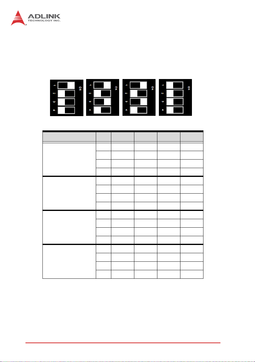
4.9 Switch and Jumper Settings
Clear CMOS Switch (SW4)
The cPCI-3615 comes with a Clear CMOS switch to reset the
CMOS values to default. The switch is located on solder side of
the board, under the "CE" logo. Press the switch to clear the
CMOS and reset the values to default.
VGA/GPIO Mode Switches (SW1, SW3)
The VGA and GPIO 4~7 signals to J2 share the same pins and
are selected by switch settings. SW1 is located on the
cPCI-3615 component side (see “cPCI-3615 Blade Board Layout” on page 19 and “Removing the DB-3610CF Daughter
Board” on page 59) and SW3 is located on the solder side
behind SW1. When the switches are set to VGA mode, the
VGA signals are available to J2, and there are only four GPIO
signals connected to J2 (GPIO 0~3). When the switches are
set to GPIO mode, there are eight GPIO signals connected to
J2 and VGA output to the RTM is not available. The switches
are set to VGA mode by default.
cPCI-3615
SW1 SW3
Mode SW1 SW3
VGA (default) All OFF All ON
GPIO 4~7 All ON All OFF
Table 4-19: VGA/GPIO Mode Switch Settings
To enable VGA output on the RTM, Onboard VGA Output Select
must be set to Rear in the BIOS Advanced Chipset Settings.
NOTE:
NOTE:
Board Interfaces 41
Page 56

COM1 Mode Selection Switches (SW1~SW4)
These switches select COM1 (cPCI-3615D/P front panel) to be
RS-232 full modem, RS-422, RS-485, or RS-485+ half-duplex
mode. Switches SW1~SW4 are located on the top edge of the
DB-3610L2 board. RS-232 full modem is set by default.
SW1 SW2 SW3 SW4
Mode Pin SW1 SW2 SW3 SW4
1ONONONOFF
RS-232
RS-422
RS-485
RS-485+
Table 4-20: COM1 Mode Selection Switch Settings
2 OFF OFF OFF OFF
3 OFF ON ON OFF
4 OFF OFF OFF OFF
1 OFF OFF OFF ON
2ONONONOFF
3 OFF OFF OFF ON
4 OFF ON ON OFF
1 OFF OFF OFF ON
2 OFF ON ON OFF
3ONOFFOFFON
4 OFF ON ON OFF
1 OFF OFF OFF OFF
2 OFF ON ON ON
3ONOFFOFFOFF
4 OFF ON ON ON
42 Board Interfaces
Page 57

cPCI-3615
COM2 Mode Selection Switches on RTM (SW1~SW4)
These switches on the RTM select COM2 to be RS-232 full
modem, RS-422, RS-485, or RS-485+ half-duplex mode.
RS-232 full modem is set by default. See “cPCI-R3610T RTM
Board Layout” on page 25 for switch locations.
SW1 SW2 SW3 SW4
Mode Pin SW1 SW2 SW3 SW4
1 OFF ON ON ON
RS-232
RS-422
RS-485
RS-485+
Table 4-21: COM2 Mode Selection Switch Settings
2OFFOFFOFFOFF
3 OFF ON ON OFF
4OFFOFFOFFOFF
1ONOFFOFFOFF
2 OFF ON ON ON
3ONOFFOFFOFF
4 OFF ON ON OFF
1ONOFFOFFOFF
2 OFF ON ON OFF
3ONOFFOFFON
4 OFF ON ON OFF
1OFFOFFOFFOFF
2ON ON ONOFF
3 OFF OFF OFF ON
4ON ON ONOFF
Board Interfaces 43
Page 58
COM3 Mode Selection Switches on RTM (SW5~SW8)
These switches on the RTM select COM3 to be RS-232 full
modem, RS-422, RS-485, or RS-485+ half-duplex mode.
RS-232 full modem is set by default. See “cPCI-R3610T RTM
Board Layout” on page 25 for switch loc at ion s.
SW5 SW6 SW7 SW8
Mode Pin SW5 SW6 SW7 SW8
1 OFF ON ON ON
RS-232
RS-422
RS-485
RS-485+
Table 4-22: COM3 Mode Selection Switch Settings
2 OFF OFF OFF OFF
3 OFF ON ON OFF
4 OFF OFF OFF OFF
1ONOFFOFFOFF
2 OFF ON ON ON
3ONOFFOFFOFF
4 OFF ON ON OFF
1ONOFFOFFOFF
2 OFF ON ON OFF
3ONOFFOFFON
4 OFF ON ON OFF
1 OFF OFF OFF OFF
2ONONONOFF
3 OFF OFF OFF ON
4ONONONOFF
44 Board Interfaces
Page 59

cPCI-3615
XMC VPWR Select Jumper on DB-3UMC (JPX1)
This jumper is located on the DB-3UMC board near JN1/2 and
selects the XMC VPWR setting. 5V is set by default.
Mode Connection JPX1
+5V (Default) 1 – 2
+12V 2 – 3
Table 4-23: XMC VPWR Select Jumper Settings
PMC V(I/O) Select Jumper on DB-3UMC (JPX2)
This jumper is located on the DB-3UMC board near JN1/2 and
selects the PMC V(I/O) setting. 3.3V is set by default.
Mode Connection JPX2
+5V 1 – 2
+3.3V (Default) 2 – 3
Table 4-24: PMC V(I/O) Select Jumper Settings
Board Interfaces 45
Page 60

This page intentionally left blank.
46 Board Interfaces
Page 61

5 Getting Started
This chapter describes the installation procedures for the
cPCI-3615 and rear transition module:
X 2.5” SATA Hard Drive Disk installation
X PCI Mezzanine Card installation
X cPCI-3615 installation to chassis
X RTM installation to chassis
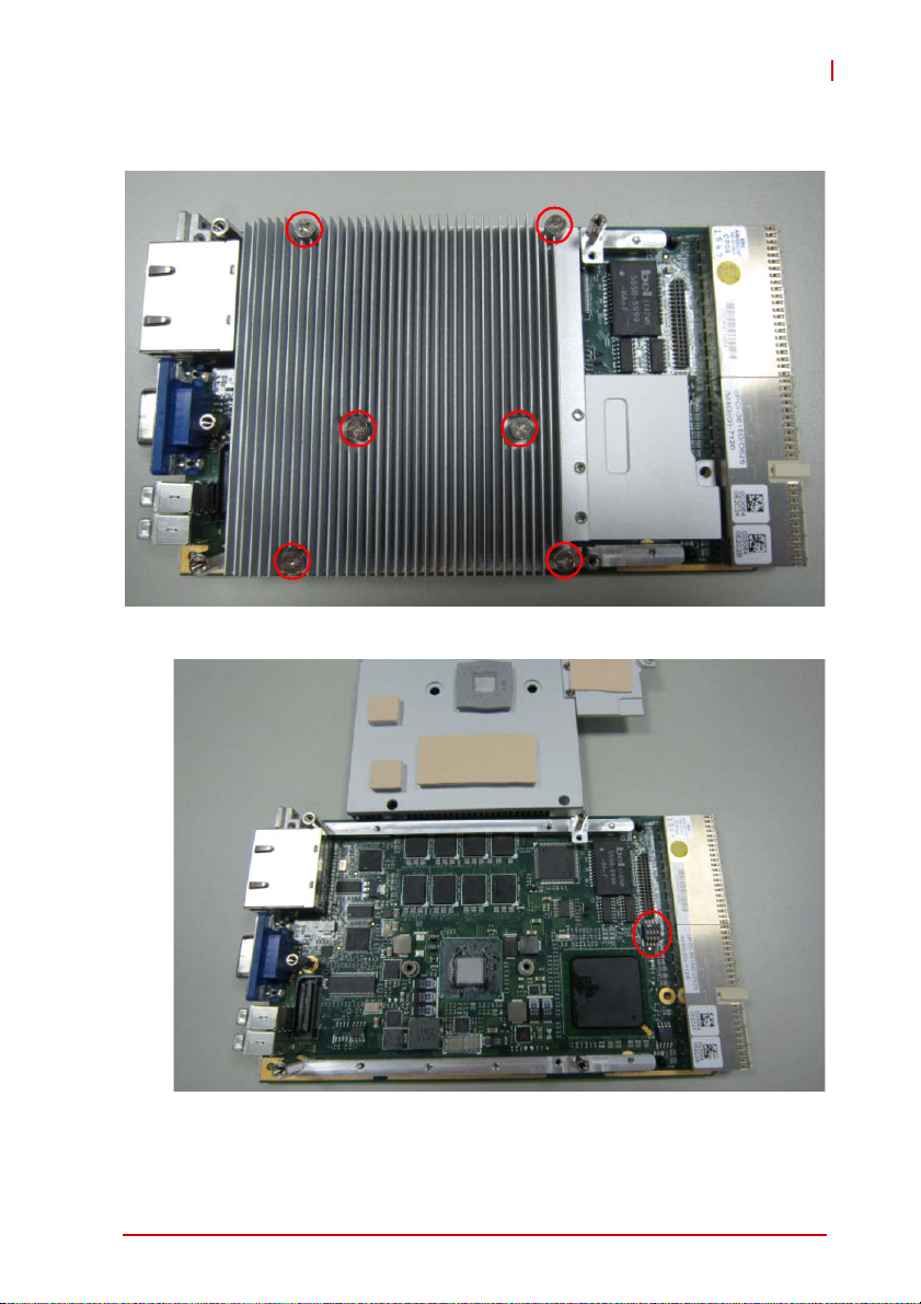
5.1 CPU and Heatsink
The cPCI-3615 Series come with a BGA CPU soldered onboard
and heatsink pre-installed. Removal of heatsink/CPU by users is not
recommended. Please contact your ADLINK service representative
for assistance.
cPCI-3615
Getting Started 47
Page 62
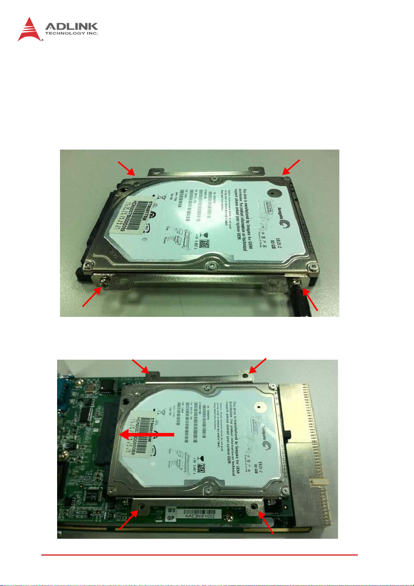
5.2 Hard Drive Installation
The cPCI-3615D/P 2/3 slot versions provide space to install a slim
type 2.5” Serial-ATA hard drive.
Installing a Hard Drive - cPCI-3615D
1. Attach the mounting brackets to the hard drive with four
M3 screws provided.
2. Align the hard drive assemby with the mounting points
on the cPCI-3615D and insert it into the onboard Serial
ATA connector until it is properly seated.
48 Getting Started
Page 63
cPCI-3615
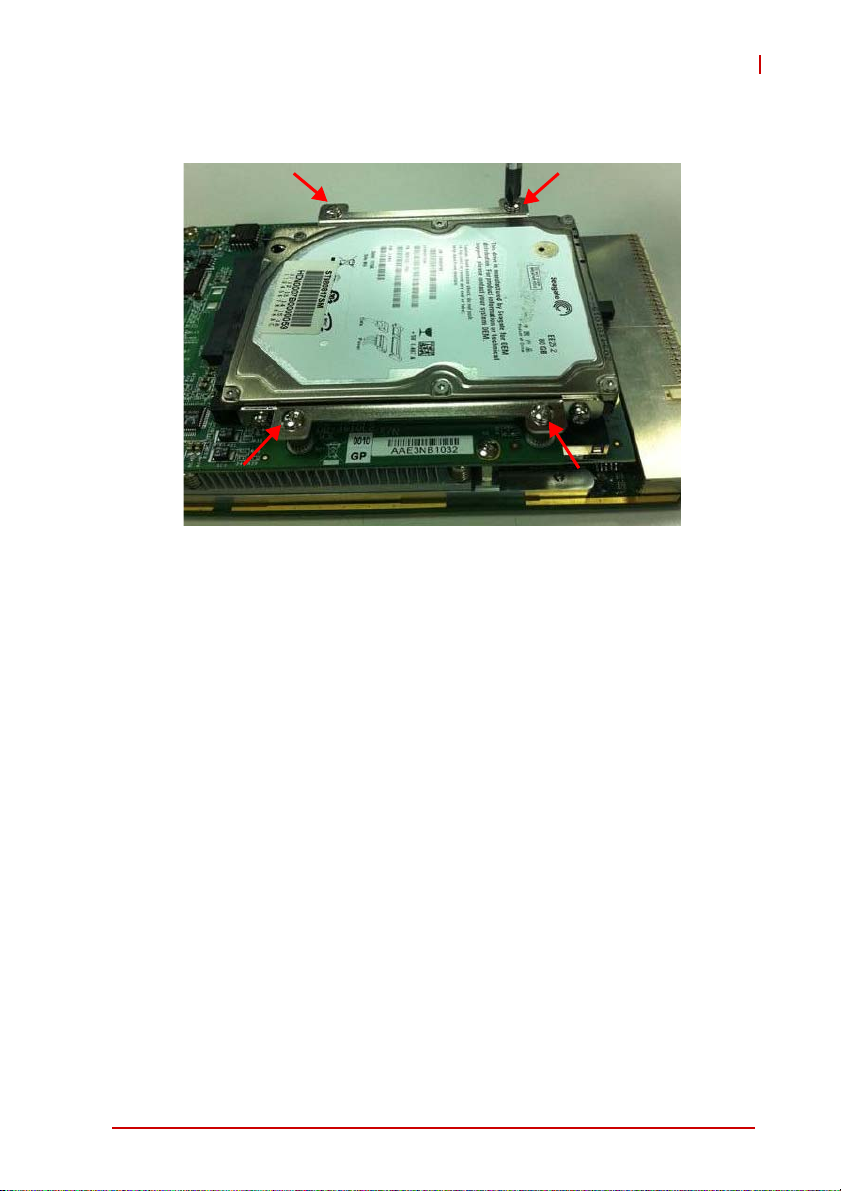
3. Secure the hard drive assemby to the cPCI-3615D using
four M2.5 screws provided.
Getting Started 49
Page 64

Installing a Hard Drive - cPCI-3615P
1. To install a hard drive on the cPCI-3615P, the front panel
and DB-3UMC daughter board must first be disassembled.
Remove the front panel by unscrewing
securing it to the PCB assembly (arrows), the four standoffs securing the VGA and COM connectors (circles),
and one screw under the ejector handle.
the four screws
50 Getting Started
Page 65

cPCI-3615
2. Detach the faceplate from the PCB assembly.
3. Loosen the five screws securing DB-3UMC riser card to
the PCB assembly.
Getting Started 51
Page 66

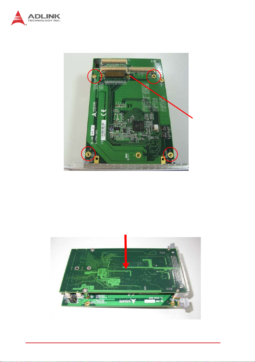
4. Remove the DB-3UMC riser card, taking care to lift it
from the board-to-board connector indicated below.
5. Attach the mounting brackets to the hard drive with four
M3 screws provided.
52 Getting Started
Page 67

cPCI-3615
6. Align the hard drive assemby with the mounting points
on the cPCI-3615P and insert it into the onboard Serial
ATA connector until it is properly seated.
7. Secure the hard drive assemby to the cPCI-3615P using
four M2.5 screws provided.
Getting Started 53
Page 68

8. Re-attach the DB-3 UMC riser card to the PCB assembly,
taking care to press down firmly on the board-to-board
connector.
9. Re-attach the faceplate to the cPCI-3615P by fastening
the four screws and four standoffs removed in Step 1
above.
54 Getting Started
Page 69

cPCI-3615
5.3 PMC/XMC Card Installation
The cPCI-3615P provides one PMC/XMC slot designed to suppo rt
3.3V or 5V V(I/O) (default 3.3V) and 5V or 12V VPWR (default
5V). Before you install the PMC/XMC card on the cPCI-3615P,
please make sure that the PMC V(I/O) jumper JPX2 and XMC
VPWR jumper JPX1 have been correctly set (see page 45).
1.
To install a PMC/XMC card on the cPCI-3615P, the front
panel and DB-3UMC daughter board must first be disassembled. Remove the front panel by uns crewing
securing it to the PCB assembly (arrows), the four standoffs securing the VGA and COM connectors (circles),
one screw under the ejector handle.
the four screws
and
Getting Started 55
Page 70
2. Remove the DB-3UMC daughter board by unscrewing
the four screws as shown below.
3.3V Key
3. There is a 3.3V key on board by de fault, if the PMC/XMC
This page intentionally left blank.
card you wish to install is 5V signaling, please remove
the key and set the PMC V(I/O) jumper JPX2 to the 5V
setting.
4. Align the male connectors of the PMC/XMC card (component-side down) to the female connectors of the
DB-3UMC and press down.
56 Getting Started
Page 71

cPCI-3615
5. Secure the PMC/XMC card to the DB-3UMC by attach-
ing four screws (provided with the card) from the underside of the daughter board.
6. Align the male board-to-board connector (CN1) of the
PMC/XMC assembly to the female board to board connector (CN7) of the DB-3610L2 riser card and press
down.
Getting Started 57
Page 72

7. Secure the PMC/XMC assembly to the DB-3610L2 riser
card using the four screws removed in Step 2 above.
8. Remove the PMC filler faceplate from the front panel.
9. Assemble the front panel to the cPCI-3615P by reversing Step 1.
58 Getting Started
Page 73

cPCI-3615
5.4 Removing the DB-3610CF Daughter Board
To access SW1 (VGA/GPIO Mode Switch) which is under the
DB-3610CF Daughter Board, follow the steps below (see
“cPCI-3615 Blade Assembly Layout” on page 20 for DB-3610CF
location).
1.
Remove the front panel from the blade assembly by
unscrewing
version shown).
2.
Remove the Layer 2 daughter board by unscrewing the five
screws as shown below (not required fo r single-slot version).
the screws and standoffs as shown (dual-slot
Getting Started 59
Page 74

3. Remove the screw securing the DB-3610CF from the
component side of the blade as shown.
4. Remove the screw securing the DB-3610CF from the
solder side of the blade as shown.
5. Remove the DB-3610CF from the blade assembly.
60 Getting Started
Page 75
cPCI-3615
6. Remove the six screws securing the heatsink to the
blade assembly
7. Remove the heatsink to access SW1.
To reassemble the cPCI-3615 blade, reverse Steps 1~7 above.
Getting Started 61
Page 76

5.5 Installing the cPCI-3615 to the Chassis
The cPCI-3615 may only be installed in a system slot of a 3U
CompactPCI chassis. These instructions are for reference only.
Refer to the user guide that comes with the chassis for more information.
1. Be sure to select the correct slot depending on the operational purpose of the module. The system power may
now be powered on or off.
2. Remove the blank face cover from the selected slot, if
necessary.
3. Press down on the release catches of the cPCI-3615
ejector handles.
4. Remove the black plastic caps securing the mounting
screws to the front panel.
5. Align the blade’s top and bottom edges to the chassis
card guides, and then carefully slide the blade into the
chassis. A slight resistance may be felt when inserting
the blade. If the resistance it too strong, check if there
are bent pins on the backplane or if the board’s connector pins are not properly aligned with connectors on the
backplane. Then push the board until it is completely
flush with the chassis.
6. Push the ejector handle outwards to secure the blade in
place, and then fasten the screws on the front panel.
7. Connect the cables and peripherals to the board, and
then turn the chassis on if necessary.
62 Getting Started
Page 77

cPCI-3615
5.6 RTM Installation - cPCI-R3610(T)
The installation and removal procedures for a RTM are the same
as those for CompactPCI boards. Because they are shorter than
front boards, pay careful attention when inserting or removing
RTMs.
Refer to previous sections for peripheral connectivity of all
I/O ports on the RTM. When installing the cPCI-3615 Series and
related RTMs, make sure the RTM is the correct matching model.
You must install the correct RTM to enable functions (I/O interfaces) on the rear panel. Installation of non-compatible RTMs
NOTE:
NOTE:
may damage the system board and/or other RTMs.
Getting Started 63
Page 78

This page intentionally left blank.
64 Getting Started
Page 79

6 Driver Installation
The cPCI-3615 drivers are available from the ADLINK All-In-One
CD at X:\cPCI\cPCI-3615\, or from the ADLINK website
(http://www.adlinktech.com). This section describes the driver
installation procedures for Windows® 7.
1. Install the Windows operating system before installing
any driver. Most standard I/O device drivers are installed
during Windows installation.
2. Install the chipset driver by running the program
...\Chipset\Intel_INF_Update_Utility_All_WinOS
v9.1.1.1023.zip.
3. Install the VGA driver and utilities by running the program
...\Graphics\
Intel_Graphics_Adapter_Win7_64_v8.14.10.2230.zip.
4. Install the LAN driver by running the program
…\LAN\Intel_Network_Adapter_Win7_64_v11.4.7.0.zip.
5. Install the Audio driver by running the program
…\Audio\Win2KXP2003_32_64_ bits.exe
We recommend using the drivers provided on the ADLINK
All-in-One CD or downloaded from the ADLINK website to ensure
compatibility. Please download the VxWorks BSP from the
ADLINK website.
cPCI-3615
Driver Installation 65
Page 80

This page intentionally left blank.
66 Driver Installation
Page 81

7 Utilities
7.1 Watchdog Timer
This section describes the operation of the cPCI-3615’s watchdog
timer (WDT). The primary function of the WDT is to monitor the
cPCI-3615's operation and to reset the system if a software application fails to function as prog rammed. The following WDT functions may be controlled using a software application:
X enabling and disabling
X reloading timeout value
The cPCI-3615 custom WDT circuit is implemented using the
internal I/O of the ITE SuperIO IT8783 which is at 2Eh of LPC. The
basic functions of the WDT include:
X Starting the timer countdown
X Enabling or disabling WDT
X Enabling or disabling WDT countdown LED ON
X Reloading the timeout value to keep the watchdog from tim-
ing out
X Setting the range of the timeout period from 1 second or minute
to maximum 65635 seconds or minutes
X Sending a RESET signal to the system when the watchdog
times out
cPCI-3615
Using the Watchdog in an Application
The following section describes using the WDT functions in an
application. The WDT reset function is explained in the previous
section. This can be controlled through the registers in the
cPCI-3615's SuperIO.
An application using the reset fe ature enab les the watch dog func tion, sets the count-down period, and reloads the timeout value
periodically to keep it from resetting the system. If the timer countdown value is not reloaded, the watchdog resets the system hardware after its counter reaches zero.
For a detailed programming sample, refer to the sample code provided in the ADLINK All-In-One CD. You can find it in the following
directory: X:\cPCI\cPCI-3615\WDT.
Utilities 67
Page 82

Sample Code
The sample program written in C shown below offers an interactive way to test the Watchdog Timer under DOS.
#include<stdio.h>
#include<dos.h>
#define IT8783_ID1 0x87
#define IT8783_ID2 0x83
static unsigned int IT8783_ioPort = 0x2e;
//Check index port
void Enter_IT8783_Config(unsigned int flag)
{
if(flag) IT8783_ioPort = 0x4e;
switch(IT8783_ioPort)
{
case 0x2E: //Address port = 0x2E, enter keys =
0x87, 0x01, 0x55, 0x55
outportb(0x2E, 0x87);
outportb(0x2E, 0x01);
outportb(0x2E, 0x55);
outportb(0x2E, 0x55);
break;
case 0x4E: //Address port = 0x4E, enter keys =
0x87, 0x01, 0x55, 0xAA
outportb(0x4E, 0x87);
outportb(0x4E, 0x01);
outportb(0x4E, 0x55);
outportb(0x4E, 0xAA);
break;
default:
break;
}
}
//Exit index port
void Exit_IT8783_Config(unsigned int flag)
{
if(flag) IT8783_ioPort = 0x4e;
68 Utilities
Page 83

cPCI-3615
outportb(IT8783_ioPort, 0x02);
outportb(IT8783_ioPort+1, 0x02);
}
//Check chip
void Get_IT8783_ID(unsigned int &ID1, unsigned int &ID2)
{
outportb(IT8783_ioPort, 0x20);
ID1 = inportb(IT8783_ioPort+1);
outportb(IT8783_ioPort, 0x21);
ID2 = inportb(IT8783_ioPort+1);
}
//WDT and LED program
void IT8783_3_WDTRun(unsigned int count_value, unsigned
int PLEDflag) //for cPCI-3615
{
unsigned long tempCount;
unsigned int registerValue;
outportb(IT8783_ioPort, 0x07);
outportb(IT8783_ioPort+1, 0x07);// Device 7
outportb(IT8783_ioPort, 0xf8);
outportb(IT8783_ioPort+1, 0x00);// PLED mapping to
nothing, disable PLED function
if(PLEDflag == 1)
{
outportb(IT8783_ioPort, 0x2D);
registerValue = inportb(IT8783_ioPort + 1);
registerValue |= 0x01; // set Pin109 is GPIO
function GP60
outportb(IT8783_ioPort+1, registerValue);
outportb(IT8783_ioPort, 0xC5);
registerValue = inportb(IT8783_ioPort + 1);
registerValue &= 0xfe; // set GP60 is alternate
function
Utilities 69
Page 84

outportb(IT8783_ioPort+1, registerValue);
outportb(IT8783_ioPort, 0xCD);
registerValue = inportb(IT8783_ioPort + 1);
registerValue |= 0x01; // set GP60 is output
outportb(IT8783_ioPort+1, registerValue);
outportb(IT8783_ioPort, 0xf8);
outportb(IT8783_ioPort+1, 0x30);// PLED mapping to
GP60
outportb(IT8783_ioPort, 0xf9);
registerValue = inportb(IT8783_ioPort + 1);
registerValue |= 0x02;
registerValue &= 0xfb;
outportb(IT8783_ioPort+1, registerValue);
}
outportb(IT8783_ioPort, 0x71);
registerValue = inportb(IT8783_ioPort + 1);
registerValue |= 0xD0; // set Mouse & Keyboard
interrupt Enable
outportb(IT8783_ioPort+1, registerValue);
outportb(IT8783_ioPort, 0x73);
outportb(IT8783_ioPort+1, count_value); // set WDT
count LSB
tempCount = tempCount >> 8;
outportb(IT8783_ioPort, 0x74);
outportb(IT8783_ioPort+1, count_value); // set WDT
count MSB
if(count_value >= 60)
{
outportb(IT8783_ioPort, 0x72);
registerValue = inportb(IT8783_ioPort+1);
registerValue &= 0x8f;
registerValue |= 0x10; //enable WDT output through
PowerOK!
outportb(IT8783_ioPort+1, registerValue); // set
WDT count is minute
tempCount = count_value / 60;
if((count_value%60) > 30)
70 Utilities
Page 85

tempCount++;
if(tempCount > 65535)
tempCount = 65535;
printf("WDT timeout in %d minutes.\n", tempCount);
}
else
{
outportb(IT8783_ioPort, 0x72);
registerValue = inportb(IT8783_ioPort+1);
registerValue |= 0x80;
tempCount = count_value;
if(tempCount != 0)
{
printf("WDT timeout in %d seconds.\n",
tempCount);
registerValue |= 0x40; //Enable WDT output
through KBRST
}
else
{
printf("WDT is Disabled.\n");
registerValue &= 0xbf; //Disable WDT output
through KBRST
}
cPCI-3615
outportb(IT8783_ioPort+1, registerValue); // set
WDT count is second
}
}
Utilities 71
Page 86

7.2 Preboot Execution Environment (PXE)
The cPCI-3615 Series supports the Intel® Preboot Execution
Environment (PXE) that is capable of booting up or executing an
OS installation through an Ethernet ports. To use PXE, there must
be a DHCP server on the network with one or more servers running PXE and MTFTP services. It could be a Windows® 2003
server running DHCP, PXE, and MTFTP services or a dedicated
DHCP server with one or more additional servers running PXE
and MTFTP services.
To build a network environment with PXE support:
1. Setup a DHCP server with PXE tag configuration
2. Install the PXE and MTFTP services
3. Make a boot image file on the PXE server (i.e. the boot server)
4. Enable the PXE boot function on the client computer
72 Utilities
Page 87

8 BIOS Setup
The following chapter describes basic navigation for the
AMIBIOS®8 BIOS setup utility.
8.1 Starting the BIOS
To enter the setup screen, follow these steps:
1. Power on the motherboard
2. Press the < Delete > key on your keyboard when you
see the following text prompt:
< Press DEL to run Setup >
3. After you press the < Delete > key, the main BIOS setup
menu displays. You can access the other setup screens
from the main BIOS setup menu , such as Chipset and
Power menus.
cPCI-3615
Note: In most cases, the < Delete > key is used to invoke the setup
screen. There are several cases that use other keys, such as
< F1 >, < F2 >, and so on.
BIOS Setup 73
Page 88

Setup Menu
The main BIOS setup menu is the first screen that you can navigate. Each main BIOS setup menu option is described in this
user’s guide.
The Main BIOS setup menu screen has two main frames. The left
frame displays all the options that can be configured. “Grayed”
options cannot be configured, “Blue” options can be.
The right frame displays the key legend. Above the key legend is
an area reserved for a text message. When an option is selected
in the left frame, it is highlighted in white. Often a text message will
accompany it.
Navigation
The BIOS setup/utility uses a key-based navigation system called
hot keys. Most of the BIOS setup utility hot keys can be used at
any time during the setup navigation process.
These keys include < F1 >, < F10 >, < Enter >, < ESC >, < Arrow >
keys, and so on. .
74 BIOS Setup
Page 89

cPCI-3615
Note: There is a hot key legend located in the r ight frame on most
setup screens.
The < F8 > key on your keyboard is the Fail-Safe key. It is not displayed on the key legend by default. To set the Fail-Safe settings
of the BIOS, press the < F8 > key on your keyboard. It is located
on the upper row of a standard 101 keyboard. The Fail-Safe settings allow the motherboard to boot up with the least amount of
options set. This can lessen the probability of conflicting settings.
Hotkey Descriptions
F1 The < F1 > key allows you to display the General Help
screen.
Press the < F1 > key to open the General Help screen.
BIOS Setup 75
Page 90

F10 T h e < F1 0 > key allows yo u to save any changes you have
made and exit Setup. Press the < F10 > key to save your
changes. The following screen will appear:
Press the < Enter > key to save the configuration and exit.
You can also use the < Arrow > key to select Cancel and
then press the < Enter > key to abort this functio n and return
to the previous screen.
ESC The < Esc > key allows you to discard any changes you have
made and exit the Setup. Press the < Esc > key to exit the
setup without saving your changes. The following screen will
appear:
Press the < Enter > key to discard changes and exit. You can
also use the < Arrow > key to select Cancel and then press
the < Enter > key to abort this function and return to the previous screen.
Enter The < Enter > key allows you to display or change the setup
option listed for a particular setup item. The < Enter > key
can also allow you to display the setup sub-screens.
76 BIOS Setup
Page 91

cPCI-3615
8.2 Main Setup
When you first enter the Setup Utility , you will enter the Main setup
screen. You can always return to the Main setup screen by selecting the Main tab. There are two Main Setup options. They are
described in this section. The Main BIOS Setup screen is shown
below.
System Time/System Date
Use this option to change the system time and date. Highlight System Time or System Date using the < Arrow > keys. Enter new values using the keyboard. Press the < Tab > key or the < Arrow >
keys to move between fields. The date must be entered in MM/
DD/YY format. The time is entered in HH:MM:SS format.
Note: The time is in 24-hour format. For example, 5:30 A.M. ap-
pears as 05:30:00, and 5:30 P.M. as 17:30:00.
8.3 Advanced BIOS Setup
Select the Advanced tab from the setup screen to enter the
Advanced BIOS Setup screen. You can select any of the items in
BIOS Setup 77
Page 92

the left frame of the screen to go to the sub menu for that item.
You can display an Advanced BIOS Setup option by highlighting it
using the < Arrow > keys. The Advanced BIOS Setup screen is
shown below.
The sub menus are described on the following pages.
78 BIOS Setup
Page 93

cPCI-3615
8.3.1 CPU Configuration
You can use this screen to select options for the CPU Configuration Settings. Use the up and down < Arrow > keys to select an
item. Use the < + > and < - > keys to change the value of the
selected option. A description of the selected item appears on the
right side of the screen. The settings are described on the following pages. An example of the CPU Configuration screen is shown
below.
Max CPUID Value Limit
When the computer is booted up, the operating system executes the CPUID instruction to identify the processor and its
capabilities. Before it can do so, it must first query the processor to find out the highest input value CPUID recognized. This
determines the kind of basic information CPUID can provide
the operating system. This option allows you to circumvent
problems with older operating systems.
When Enabled, the processor will limit the maximum CPUID
input value to 03h when queried, even if the processor supports a higher CPUID input value. When Disabled, the processor will return the actual maximum CPUID input value of the
processor when queried.
BIOS Setup 79
Page 94

Execute-Disable Bit Capability
Intel’s Execute Disable Bit functionality can help prevent certain classes of malicious buffer overflow attacks when combined with a supporting operating system. Exec ute Disable Bit
allows the processor to classify areas in memory where application code can execute and where it cannot. When a malicious worm attempts to insert code in the buffer, the processor
disables code execution, preventing damage and worm propagation.
Hyper-Threading Technology
This item allow you to enable or disable Hyper-Thread ing Technology.
Intel® Speedstep™ Tech
Intel® SpeedStep Technology allows the system to dynamically
adjust processor voltage and core frequency, which can result
in decreased average power consumption and decreased
average heat production.
Intel® C-State Tech
This option allows you to enable or disable Intel® C-State function.
Enhanced C-State Tech
This option allows you to enable or disable the Enhanced CState function.
80 BIOS Setup
Page 95

cPCI-3615
8.3.2 IDE Configuration
You can use this screen to select options for the IDE Configuration
Settings. Use the up and down < Arrow > keys to select an item.
Use the < + > and < - > keys to change the value of the selected
option.
ATA/IDE Configuration
This item specifies which mode the ATA/IDE channels should
be initialized in. The settings are Disabled, Compatible and
Enhanced.
Configure SAT A as
When running in Compatible mode, SATA channels can be
configured as a legacy IDE channel.
SATA1 does not support Compatible mode due to chipset
limitation.
NOTE:
NOTE:
IDE Master/Slave
Select one of the hard disk drives to configure it. Press
< Enter > to access its sub menu.
BIOS Setup 81
Page 96

8.3.3 Super IO Configuration
You can use this screen to select options for the Super IO settings.
Use the up and down < Arrow > keys to select an item. Use the <
+ > and < - > keys to change the value of the selected option. The
settings are described on the following pages. The screen is
shown below.
Serial Port1/2 Address
Select an address for Serial Port1/2.
Port1 Options: 3F8, 3E8, 2E8, Disabled.
Port2 Options: 2F8, 3E8, 2E8, Disabled.
Serial Port1/2 IRQ
Select an IRQ for Serial Port1/2.
Options: 3, 4, 10, 11.
Serial Port3
Enable or disable Serial Port3 (address/IRQ: 3E8/10).
82 BIOS Setup
Page 97

cPCI-3615
8.3.4 Hardware Health Configuration
This option displays the current status of all of the monitored hardware devices/components such as voltages and temperatures.
The options are Enabled and Disabled.
BIOS Setup 83
Page 98

8.3.5 USB Configuration
You can use this screen to select options for the USB Configuration. Use the up and down < Arrow > keys to select an item. Use
the < + > and < - > keys to change the value of the selected
option. The settings are described on the following pages. The
screen is shown below.
Legacy USB Support
Legacy USB Support refers to USB mouse and keyboard support. Normally if this option is not enabled, any attached USB
mouse or USB keyboard will not become available until a USB
compatible operating system is fully booted with all USB drivers loaded. When this option is enabled, any attached USB
mouse or USB keyboard can control the system even when
there are no USB drivers loaded on the system. Set this value
to enable or disable the Legacy USB Support.
X Disabled: Set this value to prevent the use of any USB
device in DOS or during system boot.
X Enabled: Set this value to allow the use of USB devices
during boot and while using DOS.
84 BIOS Setup
Page 99

cPCI-3615
X Auto: This option auto detects USB Keyboards or M ice and
if found, allows them to be utilized during boot and while
using DOS.
USB 2.0 Controller Mode
The USB 2.0 Controller Mode c onfigures the data rate of the
USB port. The options are FullSpeed (12 Mbps) and HiSpeed
(480 Mbps).
USB Functions
Set the value to allow the system to disable, enabled and
select a set number of onboard USB ports.
USB 2.0 Controller
Enable or disable USB 2.0 functionality to all USB ports.
USB Mass Storage Device Configuration
This is a submenu for configuring the USB Mass Stor age Class
Devices when BIOS finds they are in use on USB ports. Emulation Type can be set according to the type of attached USB
mass storage device(s). If set to Auto, USB devices less than
530MB will be emulated as Floppy and those greater than
530MB will remain as hard drive. The Forced FDD option can
be used to force a hard disk type drive (such as a Zip drive) to
boot as FDD.
BIOS Setup 85
Page 100

8.3.6 AHCI Configuration
You can use this screen to select options for the AHCI Settings.
Use the up and down < Arrow > keys to select an item. Use the <
+ > and < - > keys to change the value of the selected option.
SATA Port0/1/2
Select the type of device connected to the system.
S.M.A.R.T
S.M.A.R.T. (Self-Monitoring Analysis and Reporting Technology) is a utility that monitors your disk status to predict hard
disk failure.
86 BIOS Setup
 Loading...