

Page 1
cPCI-3510 Series
Performance 3U CompactPCI® PlusIO
Intel® Core™ i7/i5 Processor Blade
User’s Manual
Manual Rev.: 2.01
Revision Date: November 17, 2014
Part No: 50-15095-1010
Advance Technologies; Automate the World.
Page 2

Revision History
Revision Release Date Description of Change(s)
2.00 26/03/2014 Initial release
2.01 17/11/2014 Correct Block Diagram SATA device support
ii Revision History
Page 3

cPCI-3510
Preface
Copyright 2014 ADLINK Technology Inc.
This document contains proprietary infor mation protected by copyright. All rights are reserved. No part of this manual may be reproduced by any mechanical, electronic, or other means in any form
without prior written permission of the manufacturer.
Disclaimer
The information in this document is subject to change without prior
notice in order to improve reliability, design, and function and does
not represent a commitment on the part of the manufa cturer.
In no event will the manufacturer be liable for direct, indirect, special, incidental, or consequential damages arising out of the use or
inability to use the product or documentation, even if advised of
the possibility of such damages.
Environmental Responsibility
ADLINK is committed to fulfill its social responsibility to global
environmental preservation through compliance with the European Union's Restriction of Hazardous Substances (RoHS) directive and Waste Electrical and Electronic Equipment (WEEE)
directive. Environmental protection is a top priority for ADLINK.
We have enforced measures to ensure that our products, manufacturing processes, components, and raw materials have as little
impact on the environment as possible. When products are at their
end of life, our customers are encouraged to dispose of them in
accordance with the product disposal and/or recovery programs
prescribed by their nation or company.
Trademarks
Product names mentioned herein are used for identification purposes only and may be trademarks and/or registered trademarks
of their respective companies.
Preface iii
Page 4

Using this Manual
Audience and Scope
The cPCI-3510 User’s Manual is intended for hardware
technicians and systems operators with knowledge of installing,
configuring and operating industrial grade single boar d computers.
Manual Organization
This manual is organized as follows:
Chapter 1, Introduction: Introduces the cPCI-3510, its features,
block diagrams, and package contents.
Chapter 2, Specifications: Presents detailed specification infor-
mation, power consumption, and technical drawings.
Chapter 3, Functional Description: Describes the cPCI-3510
main functions.
Chapter 4, Board Interfaces: Describes the cPCI-3510 board
interfaces.
Chapter 5, Getting Started: Describes the installation of compo-
nents to the cPCI-3510 and rear transition modules.
Chapter 6, Driver Installation: Provides information on how to
install the cPCI-3510 device drivers under Windows 7.
Chapter 7, Watchdog Timer: Describes the watchdog timer of
the cPCI-3510.
Chapter 8, BIOS Setup Utility: Describes basic navigation for the
AMI EFI BIOS setup utility.
Chapter 9, IPMI User Guide: Provides information on the base-
board management controller (BMC) of the Intelligent Platform
Management Interface (IPMI).
Important Safety Instructions: Presents safety instructions all
users must follow for the proper setup, installation and usage of
equipment and/or software.
Getting Service: Contact information for ADLINK’s worldwide
offices.
iv Preface
Page 5
cPCI-3510
Conventions
Take note of the following conventions used throughout this
manual to make sure that users perform certain tasks and
instructions properly.
Additional information, aids, and tips that help users perform
tasks.
NOTE:
NOTE:
Information to prevent minor physical injury, component damage, data loss, and/or program corruption when trying to com-
CAUTION:
WARNING:
plete a task.
Information to prevent serious physical injury, component
damage, data loss, and/or program corruption when trying to
complete a specific task.
Preface v
Page 6

This page intentionally left blank.
vi Preface
Page 7

cPCI-3510
Table of Contents
Revision History...................................................................... ii
Preface.................................................................................... iii
List of Figures........................................................................ xi
List of Tables........................................................................ xiii
1 Introduction ........................................................................ 1
1.1 Overview.............................................................................. 1
1.2 Features............................................................................... 2
1.3 Model Number Decoder....................................................... 3
1.4 Package Contents ............................................................... 5
2 Specifications..................................................................... 7
2.1 cPCI-3510 Processor Blade Specifications.................. .... ... 7
2.2 cPCI-R3P00(T) RTM Specifications.................................. 11
2.3 Block Diagrams.................................................................. 12
2.4 I/O Connectivity Table ....................................................... 19
2.5 Power Requirements.................... ... .... ... ... ... ... .... ... ... ... .... . 21
3 Functional Description .................................................... 23
3.1 Processors......................................................................... 23
3.2 Platform Controller Hub ..................................................... 25
3.3 PMC/XMC.......................................................................... 25
3.4 Intel® Turbo Boost Technology......................................... 26
3.5 Intel® Hyper-Threading Technology.................................. 26
3.6 Trusted Platform Module ................................................... 26
3.7 Battery ............................................................................... 27
4 Board Interfaces............................................................... 29
vii
Page 8

4.1 cPCI-3510 Series Board Layout ..................................... ... 29
4.2 cPCI-3510 Blade Assembly Layout ................................... 31
4.3 cPCI-3510D Blade Assembly Layout................................. 32
4.4 cPCI-3510G Blade Assembly Layout................................. 33
4.5 cPCI-3510L Blade Assembly Layout ................................. 34
4.6 cPCI-3510M Blade Assembly Layout ................................ 35
4.7 cPCI-3510, cPCI-3510D, cPCI-3510G Faceplate.............. 36
4.8 cPCI-3510L, cPCI-3510M Front Panel .............................. 37
4.9 cPCI-R3P00(T) RTM Board Layout................................... 39
4.10 cPCI-R3P00(T) RTM Faceplate......................................... 40
4.11 Connector Pin Assignments............................................... 41
4.12 Jumper Settings................................................................. 66
5 Getting Started.................................................................. 67
5.1 CPU and Heatsink ............................................................. 67
5.2 SATA Drive Installation...................................................... 68
5.3 Installing a CFast Card ......................................... .... ... ... ... 71
5.4 Installing the cPCI-3510 to the Chassis............................. 72
5.5 RTM Installation - cPCI-R3P00(T)..................................... 73
6 Driver Installation.............................................................. 75
6.1 cPCI-3510 Drivers.............................................................. 75
6.2 Ethernet Controller Driver.................................................. 76
6.3 USB-to-Serial Converter Driver (RTM) .............................. 78
7 Watchdog Timer................................................................ 81
7.1 Setting the Watchdog by IPMI Commands........................ 81
8 BIOS Setup Utility............................................................. 87
8.1 Starting the BIOS............................................................... 87
8.2 Main Setup......................................................................... 92
8.3 Advanced BIOS Setup....................................................... 93
8.3.1 ACPI Settings ................................................................94
8.3.2 Trusted Computing ........................................................95
viii
Page 9

cPCI-3510
8.3.3 CPU Configuration...... ... .... ... ... ... .... ... ... ... ... .... ... ... ... .... .. 96
8.3.4 SATA Configuration....................................................... 97
8.3.5 PCH-FW Configuration..................................................98
8.3.6 Intel ® Anti-Theft Technology Configuration............ ...... 99
8.3.7 AMT Configuration...... ... .... ... ... ... .... ... ... ... ... .... ... ... ... .... 100
8.3.8 USB Configuration....................................................... 101
8.3.9 Hardware Monitor........................................................102
8.3.10Super IO Configuration................................................ 103
8.3.11Console Redirection .................................................... 105
8.4 Chipset Setup.................................................................. 108
8.4.1 PCH-IO Configuration..................................................109
8.4.2 System Agent (SA) Configuration................................112
8.5 Boot Settings ................................................................... 116
8.5.1 CSM Parameter...........................................................117
8.6 Security Setup ................................................................. 119
8.7 Save & Exit Menu............................ .... ... ... ... ... ................ 120
9 IPMI User Guide.............................................................. 123
9.1 Introduction...................................................................... 123
9.2 Summary of Commands Supported by BMR-AVR-cPCI. 123
9.3 OEM Commands Summary Table................................... 125
9.4 CompactPCI Address Map .............................................. 128
9.5 Communications with IPMC............................................. 129
9.6 IPMI Sensors List............................................................. 129
9.7 Relevant Documents ....................................................... 130
Important Safety Instructions............................................ 131
Getting Service.................................................................... 133
ix
Page 10

This page intentionally left blank.
x
Page 11

cPCI-3510
List of Figures
Figure 2-1: cPCI-3510 Blade Functional Block Diagram..................12
Figure 2-2: DB-3610L2 Daughter Board Functional Block Diag......13
Figure 2-3: DB-3970L2 Daughter Board Functional Block Diag......14
Figure 2-4: DB-LANL2-S Daughter Board Functional Block Diag....15
Figure 2-5: DB-Max Daughter Board Functional Block Diagram..... 16
Figure 2-6: cPCI-R3P00 RTM Functional Block Diagram................17
Figure 2-7: cPCI-R3P00T RTM Functional Block Diagram.............. 18
Figure 4-1: cPCI-3510 Series Board Layout (component side) .......29
Figure 4-2: cPCI-3510 Series Board Layout (solder side) ............... 30
Figure 4-3: cPCI-3510 Blade Assembly Layout ...............................31
Figure 4-4: cPCI-3510D Blade Assembly Layout.............................32
Figure 4-5: cPCI-3510G Blade Assembly Layout ............................33
Figure 4-6: cPCI-3510L Blade Assembly Layout .............................34
Figure 4-7: cPCI-3510M Blade Assembly Layout ............................35
Figure 4-8: cPCI-3510, cPCI-3510D/G Front Panel Layout.............36
Figure 4-9: cPCI-3510L, cPCI-3510M Front Panel Layout .............. 37
Figure 4-10: cPCI-R3P00(T) RTM Board Layout............................... 39
Figure 4-11: cPCI-R3P00(T) RTM Front Panel..................................40
Figure 7-1: Example procedure for WDT over serial console.......... 85
List of Figures xi
Page 12

This page intentionally left blank.
xii List of Figures
Page 13

cPCI-3510
List of Tables
Table 2-1: cPCI-3510 Processor Blade Specifications.....................7
Table 2-2: cPCI-R3P00(T) RTM Specifications..............................11
Table 2-3: cPCI-3510 I/O Connectivity ...........................................19
Table 4-1: cPCI-3510 Front Panel System LED Descriptions ........ 38
Table 4-2: USB 2.0 Pin Definition................................................... 41
Table 4-3: VGA Pin Definition ... ... ... .... ... ... ... .... ... ... ... ... .... ... ... .........42
Table 4-4: DisplayPort Pin Definition..............................................42
Table 4-5: DVI-I Connector Pin Definition....................................... 43
Table 4-6: RJ-45 GbE Pin Definitions.............................................44
Table 4-7: LAN LED Status Definitions........................................... 44
Table 4-8: PS/2 Keyboard/Mouse Pin Definition.............................45
Table 4-9: cPCI-3510D/P COM1 (DB-9) Pin Definition...................45
Table 4-10: cPCI-3510D/P COM1 Mode Selection Switch Settings.46
Table 4-11: cPCI-3510G/T COM1 (RJ-45) Pin Definition................. 47
Table 4-12: cPCI-3510G/T COM1 (DB-9 adapter) Pin Definition.....47
Table 4-13: RS-422/485 Adapter Dongle Pin Definition ...................48
Table 4-14: cPCI-3510G/T COM1 with Dongle Pin Def’n........... .... .. 48
Table 4-15: cPCI-3510G/T COM2 Pin Header Definition ........ ... .... .. 49
Table 4-16: cPCI-R3P00 RTM COM4 Pin Definition ........................49
Table 4-17: cPCI-R3P00(T) RTM COM5 Pin Definition....................50
Table 4-18: cPCI-R3P00(T) RTM COM5 with Dongle Pin Def’n....... 50
Table 4-19: cPCI-3510M 100-pin I/O Connector Pin Definition........51
Table 4-20: SATA Connector on RTM.............................................. 53
Table 4-21: SATA Connector on DB-3610L2/3970L2 Pin Def’n....... 53
Table 4-22: CFast Socket Pin Definition........................................... 54
Table 4-23: DB-3610L2 Connector Pin Definition............................. 55
Table 4-24: DB-3CFAST Connector Pin Definition...........................56
Table 4-25: DB-3970L2 Connector Pin Definition............................. 57
Table 4-26: DB-3UMC Connector Pin Definition...............................58
Table 4-27: PMC Connector Pin Definitions..................................... 59
Table 4-28: XMC Connector Pin Definition.................... .... ... ... ... .... .. 61
Table 4-29: CompactPCI J1 Connector Pin Definition...................... 62
Table 4-30: CompactPCI J2 Connector Pin Definition...................... 63
Table 4-31: cPCI-R3P00 rJ2 Connector Pin Definition.....................64
Table 4-32: cPCI-R3P00T rJ2 Connector Pin Definition...................65
Table 4-33: Load BIOS Default Jumper Settings.............................. 66
Table 4-34: XMC VPWR Select Jumper Settings.............................66
Table 4-35: PMC V(I/O) Select Jumper Settings............................ .. 66
List of Tables xiii
Page 14

This page intentionally left blank.
xiv List of Tables
Page 15

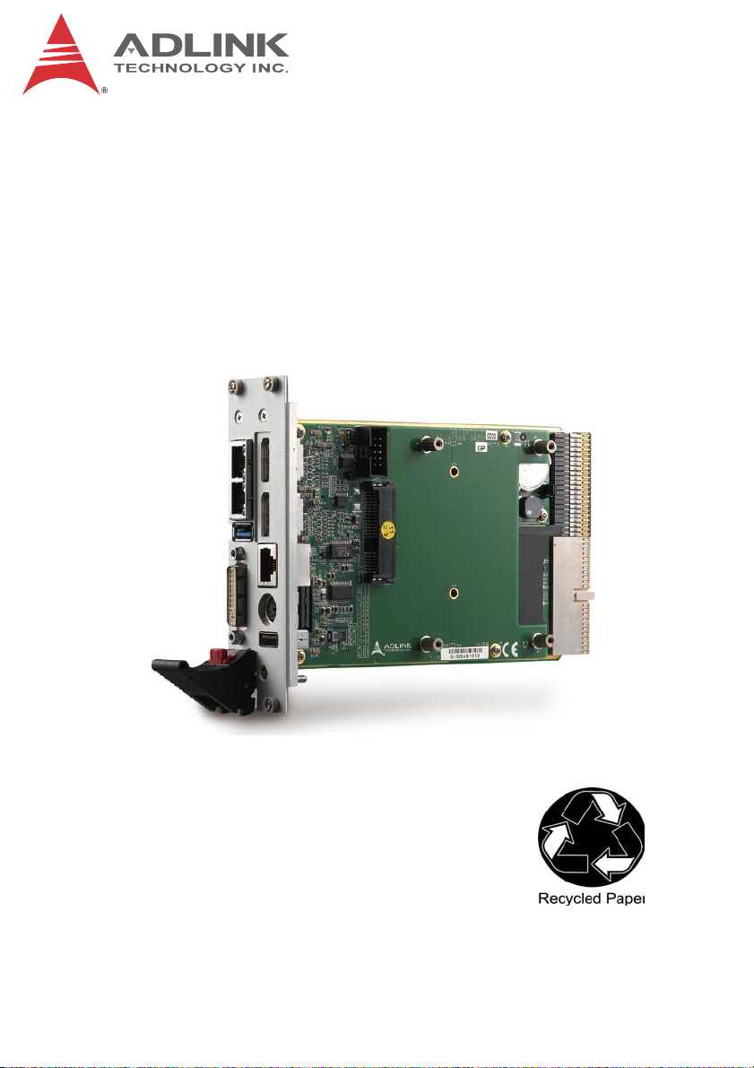
1 Introduction
1.1 Overview
The ADLINK cPCI-3510 Series is a 3U CompactPCI® PlusIO
compatible processor blade with soldered DDR3L-1600 ECC
memory up to 8GB. The ADLINK cPCI-3510 features an Intel®
Core™ i7 processor with Mobile Intel® QM87 Express Chipset.
The cPCI-3510 Series is a 3U CompactPCI blade available in single-slot (4HP), dual-slot (8HP) or triple-slot (12HP) width form factors with various daughter boards to provide a broad range of I/O
requirements. Front panel I/O in the single-slot (4HP) version
includes 1x DVI-I, 2x GbE and 1x USB 3.0 port (these I/O are
common to all versions). Front panel I/O in the dual-slot ( 8HP) version includes additional 2x USB 2.0, 1x COM, 1x KB/MS and
Line-in/Line-out on the cPCI-3510D or additional 2x DisplayPorts,
1x COM in RJ-45 connector, 1x KB/MS and 1x additional USB2.0
port on the cPCI-3510G. Two more dual-slot options are the
cPCI-3510L with additional 2x GbE, 1x COM and 2x USB and the
cPCI-3510M with one 100-pin high density connector supporting
additional 2x DVI-I/DP, 2x USB 2.0, 2x COM, 2x KB/MS and
Line-in/Line-out ports.
Graphics support is integrated on the CPU and allows 3 independent displays on the front panel by selecting the cPCI-3510G with
additional 2x DisplayPorts. Storage includes a CFast slot or a
32GB SSD (optional) and 2.5" SATA HDD on the layer 2 riser card
(cPCI-3510D/P/L/M). One optional PCI 32-bit/66 MHz PMC site or
PCIe x1 XMC site is available on the 8HP or 12HP versions
(cPCI-3510S or cPCI-3510P/T).
cPCI-3510
Rear I/O signals to J2 include 4x PCIe x1, 3x SA TA 3 Gb/s, and 3x
USB 2.0. GPIO and SMBus signals are also routed to the J2 connector. The optional Rear Transition Module (RTM) provides 3x
SATA, 2x GbE, 2x USB, 1x COM (Tx/Rx) and 1x VGA por t.
The cPCI-3510 is a high performance solution for factory automation and other industrial applications that require superior data
transfer capability and advanced computing power. The ADLINK
cPCI-3510 provides high manageability, supports Satellite mode
operation as a standalone blade in peripheral slots, and IPMI for
Introduction 1
Page 16

system health monitoring. A GbE port on the faceplate supports
Intel® AMT 9.0 for remote monitoring.
1.2 Features
X 3U CompactPCI blade in 4HP, 8HP or 12HP width form factor
X Intel® Core™ i7-4700EQ Processor (4 cores, 8 threads, 6M
cache, 2.4 GHz)
X Graphics and memory controllers integrated in processor
X Compatible with PICMG 2.30 PlusIO (3x SATA, 4x PCIe x1, 3x
USB, 2x GbE to J2)
X Dual channel DDR3L-1600 soldered SDRAM with ECC, up to
8GB
X 32bit/ 33, 66MHz CompactPCI Interface based on PCI specifi-
cations, universal V(I/O)
X Supports Satellite mode operation as a standalone blade in
peripheral slots
X Optional 32-bit/66MHz PMC or PCIe x1 XMC site
X Supports IPMI for system health monitoring
X DVI-I port on front with VGA switchable to r ear I/O by BIOS set-
ting
X Additional two DisplayPorts on 8HP daughter boar d
(cPCI-3510G)
X
Supports 3 independent displays with DirectX 11.1, OpenGL 3.2
X Two PCIe Gigabit Ethernet egress ports, one supporting Intel
iAMT 9.0
X Two additional PCIe Gigabit Ethernet Controllers routed to
RTM (cPCI-R3P00)
X Additional two Gigabit Ethernet ports on 80mm RTM
(cPCI-R3P00T)
X Line-in and Line-out ports on front panel (cPCI-3510D)
X CFast socket for SATA interface storage
X Optional onboard SSD for SATA interface storage (shares
space with CFast socket)
X 2.5" SATA drive onboard on 8HP/12HP versions at 6 Gb/s
(cPCI-3510/D/G/M/L)
2Introduction
Page 17

1.3 Model Number Decoder
Blades
cPCI-EX 3510 D / 4700 / M4G
(A) (B) (C) (D) (E)
(A) Operating Temperature Code
Z
Blank
= -20°C to +70°C
Z
ET
= -40°C to +85°C
(B) J2 Connector Type Code
Z 0 = HM connector
Z 1 = UHM connector (PICMG 2.30 PlusIO compliant)
(C) Configuration Code
Z Blank = Single slot width with CFast socket, 1x DVI-I, 1x
USB 3.0, 2x GbE
Z D = Dual slot width with CFast socket, 1x DVI-I, 1x USB 3.0,
2x GbE on layer 1; 2x USB, COM (RS-232/422/485), PS/2
KB/MS, Line-in, Line-out ports and 2.5" SATA drive space
on layer 2 DB-3610L2
Z G = Dual slot width with CFast socket, 1x DVI-I, 1x USB 3.0,
2x GbE on layer 1; 2x DisplayPort, RJ-45 COM
(RS-232/422/485), PS/2 KB/MS, USB ports, onboard SATA
connector and 2.5" SAT A dr ive sp ace on laye r 2 DB-3970L2
Z L = Dual slot width with CFast socket, 1x DVI-I, 1x USB 3.0,
2x GbE on layer 1; 2x GbE, 1x DB-9 COM
(RS-232/422/485), 1x USB2.0 at front panel, 1x onboard
USB port and 2.5" SATA drive space on layer 2 DB-LAN2-S
Z M = Dual slot width with CFast socket, 1x DVI-I, 1x USB 3.0,
2x GbE on layer 1; 1x 100-pin high density connector supports 2xDVI/DP, 2x USB2.0, 2x COM (RS-232/422/485), 1x
KB/MS, audio and 2.5" SATA drive space on layer 2
DB-Max
Z S = Dual slot width with CFast socket, 1x DVI-I, 1x USB 3.0,
2x GbE on layer 1; PMC/XMC site on layer2 DB-3UMC
(for CPUs with TDP below 37W only)
cPCI-3510
Introduction 3
Page 18

Z P =Triple slot width with CFast socket, 1x DVI-I, 1x USB 3.0,
2x GbE on layer 1; 2x USB, COM (RS-232/422/485), PS/2
KB/MS, Line-in, Line-out ports and 2.5" SATA drive space
on layer 2 DB-3610L2; PMC/XMC site in layer 3 DB-3UMC
Z T = Triple slot width with CFast socket, 1x DVI-I, 1x USB
3.0, 2x GbE on layer 1; 2x DisplayPort, RJ-45 COM, PS/2
KB/MS, USB ports, onboard SA TA connector and 2.5" SATA
drive space on layer 2 DB-3970L2; PMC/XMC site on layer
3 DB-3UMC
Z Other = ODM/OEM project code
(D) CPU Code
Z 4700EQ = Quad Core Intel® i7-4700EQ processor
(E) Memory Size Code
Z M4G = 2x 2GB DDR3L-1600 soldered SDRAM
Z M8G = 2x 4GB DDR3L-1600 soldered SDRAM
RTMs
cPCI - R3P00 T
(A)
(A) Model Code
Z Blank = dual slot width, 50mm depth 3U RTM wi th 2x COM,
2x USB, 3x SATA, VGA, 2x GbE (switched from front CPU
blade)
Z T = dual slot width, 80mm depth 3U RTM with 2x COM, 2x
USB, 3x SA TA, VGA, 2x GbE (independent from front CPU
blade)
4Introduction
Page 19

cPCI-3510
1.4 Package Contents
The cPCI-3510 is packaged with the following components. If any
of the following items are missing or damaged, retain the shipping
carton and packing material and contact the dealer for inspection.
Please obtain authorization before returning any product to
ADLINK. The packing contents of cPCI-3510 Series non-standard
configurations will vary depending on customer requests.
CPU module
X The cPCI-3510 Series Processor Blade
Z CPU and memory specifications will differ depending on
options selected
Z Thermal module is assembled on the board
X Y-cable for PS/2 combo port (8HP/12HP version only)
X 2.5" HDD accessory pack (8HP/12HP version only)
X RJ-45 to DB-9 COM adapter cable (cPCI-3510G version only)
X RS-422/485 DB-9-to-DB-9 dongle (cPCI-3510G version only)
X DisplayPort to DVI adapter cable (cPCI-3510G version only)
X ADLINK All-in-One DVD
X User’s manual
No I/O cables are included with the cPCI-3510M version.
NOTE:
NOTE:
Rear Transition Module
X cPCI-R3P00 or cPCI-R3P00T RTM
X RS-422/485 DB-9-to-DB-9 dongle
Introduction 5
Page 20
Optional Accessories
X DB-3SSD adapter for onboard SSD 32GB
Z DB-3SSD/B/NTPM (P/N 30-37581-300E)
Z DB-3SSD/B (P/N 30-37581-200E)
Z DB-3SSD/NTPM (P/N 30-37581-100E)
(B: "coin cell battery", NTPM: "no TPM")
X DisplayPort to DVI adapter cable (P/N 30-01120-0000)
X DisplayPort to VGA adapter cable (P/N 30-01119-0000)
X DisplayPort to HDMI adapter cable (P/N 30-01121-0000)
The contents of non-standard cPCI-3510 configurations may
vary depending on the customer’s requirements.
NOTE:
NOTE:
This product must be protected from static discharge and phys-
ical shock. Never remove any of the components except at a
CAUTION:
static-free workstation. Use the anti-static bag shipped with the
product when putting the board on a surface. Wear an
anti-static wrist strap properly grounded on one of the system's
ESD ground jacks when installing or servicing system compo-
nents.
6Introduction
Page 21

2 Specifications
2.1 cPCI-3510 Processor Blade Specifications
cPCI-3510
CompactPCI®
Standards
Mechanical • Standard 3U CompactPCI®
Processor • Intel® Core™ i7-4700EQ Processor, 2.4 GHz, 6MB LLC
Chipset • Mobile Intel® QM87 Express Chipset
Memory • Dual channel DDR3L-1600 ECC soldered memory
CompactPCI
Bus
Gigabit
Ethernet
Graphics • Integrated on Intel® Core™ processor
USB • Up to three USB front panel ports
• P ICMG® 2.0 CompactPCI® Rev. 3.0
• PICMG® 2.1 Hot Swap Specification Rev. 2.0
• P ICMG® 2.9 System Manag ement Rev. 1.0
• P ICMG® 2.30 CompactPCI® PlusIO
• B oard size: 100mm x 160mm
• Single slot (4HP, 20.32mm); Dual slot (8HP, 40.64mm);
Triple-slot (12HP, 60.96 mm)
• CompactPCI® with HM type J1 connector, UHM type J2
connector
cache, TDP 45W
• Passive heatsink
• Up to 8GB
• PCI 32bit/ 33MHz; 3.3V, 5V universal V I/O
• Supports operation in system slot as master or in peripheral
slot as standalone blade without connectivity to CompactPCI
bus (Satellite mode)
• One PCIe x1 Intel® I217 GbE PHY and three PCIe x1 Intel®
I210 Gigabit Ethernet controllers
• Two egress 10/100/1000BASE-T ports on front panel, one
supporting Intel® AMT 9.0 by I217 controller
• Two egress 10/100/1000BASE-T ports routed to rear
transition module
• DVI-I port on fron t panel, VGA switchable to J2 (RTM) by
BIOS setting
• A nalog monitor support up to QXGA 2048x1536 @75Hz,
32-bit
• Two DisplayPorts on front panel with resolution up to
2560x1600 @60Hz (cPCI-3510G only)
• Up to three independent display
Table 2-1: cPCI-3510 Processor Blade Specifications
Specifications 7
Page 22
Serial Ports • Up to four serial ports
• One RS-232/422/485 serial port on 8HP front panel
(cPCI-3510D/G/L)
• Additional RS-232 10-pin header on layer-2 board
(cPCI-3510G only)
• Up to two RS-232/422/485 COM port (cPCI-3510M only)
PMC/XMC • One 32-bit/66MHz PMC site or PCIe x1 XMC site if
DB-3UMC daughter board is installed
Audio • Line-in/Line-out on front panel by Realtek ALC262 High
Definition Audio codec (cPCI-3510D only)
• Line-in/Line-out on front panel by 100-pin connector
(cPCI-3510M only)
TPM Atmel AT97SC3204 TPM (upon request) supporting:
• Over/Under voltage detection
• Low/High frequency sensor/filter
• Reset filter
• Me mo r y encryption/decryption
Storage
Interfaces
• CFast socket on daughter board
1
• Optional onboard SSD on daughter board
• One SA T A 6Gb/s direct connector for 2.5" onboard HDD/SDD
(8HP/12HP version only)
BIOS • AMI® EFI BIOS, 64Mbit SPI flash memory
OS
Compatibility
• Mi crosoft Windows 7 32/64-bit
• Mi cro soft Windows 8 32/64-bit
• Red Hat Enterprise Linux 6.4, 64-bit
• Fedora 14, 32-bit
• VxWorks 6.9
• Real Time RTX (MSI)
• Other OS support upon request
Environmental • Operating Temperature (with forced air flow)2:
Standard: -20°C to 70°C
Extreme temperature: -40°C to +85°C (for Intel® Core™
i5 and Intel® Core™ i7-4700EQ processor with cTDP
down and forced air flow)
• Storage Temperature: -50°C to 100°C
• Humidity: 95% @60°C non-condensing
• Shock: 20G peak-to-peak, 11ms duration, non-operating
•Vibration
3
: 2Grms, 5-500Hz, each axis, operating (w/o hard
drive)
EMI • CE EN55022
• FCC Cla ss A
T able 2-1: cPCI-3510 Processor Blade Specifications
8 Specifications
Page 23

Faceplate I/O 4HP (cPCI-3510)
• 1x USB 3.0 ports
• 2x 10/100/1000BASE-T Ethernet ports
•1x DVI-I port
8HP (cPCI-3510D)
• 1x USB 3.0 ports
• 2x 10/100/1000BASE-T Ethernet ports
•1x DVI-I port
• 2x USB 2.0 ports
• DB-9 RS-232/422/485/485+ port
• PS/2 Keyboard/Mouse combo port
• Line-in and Line-out port
8HP (cPCI-3510G)
• 1x USB 3.0 ports
• 2x 10/100/1000BASE-T Ethernet ports
•1x DVI-I port
• 2x Displa y Port
• 1x USB 2.0 ports
• RJ-45 RS-232/422/485 port
• PS/2 Keyboard/ Mouse combo port
8HP (cPCI-3510L)
• 1x USB 3.0 ports
•1x DVI-I port
• 4x 10/100/1000BASE-T Ethernet ports
• 1x USB 2.0 ports
• DB-9 RS-232/422/485 port
8HP (cPCI-3510M)
• 1x USB 3.0 ports
•1x DVI-I port
• 2x 10/100/1000BASE-T Ethernet ports
• 1x 100-pin connector supports 2x DVI/DP, Line-in/Line-out,
2x USB 2.0, 2x RS-232/422/485 COM, 1x KB/MS
8HP (cPCI-3510S)
• 1x USB 3.0 ports
• 2x 10/100/1000BASE-T Ethernet ports
•1x DVI-I port
• PMC/XMC site
Table 2-1: cPCI-3510 Processor Blade Specifications
cPCI-3510
3
Specifications 9
Page 24

Faceplate I/O 12HP (cPCI-3510P)
• 1x USB 3.0 ports
• 2x 10/100/10 00BASE-T Ethernet ports
• 1x DVI-I port
• 2x USB 2.0 ports
• DB-9 RS-232/422/485/485+ port
• PS/2 Keyboard/Mo use combo port
• Line-in and Line-out port
• PMC/XMC site
12HP (cPCI-3510T)
• 1x USB 3.0 ports
• 2x 10/100/10 00BASE-T Ethernet ports
• 1x DVI-I port
• 2x DisplayPort
• 1x USB 2.0 ports
• RJ-45 RS-232/422/485 port1
• PS/2 Keyboard/ Mouse combo port
• PMC/XMC site
T able 2-1: cPCI-3510 Processor Blade Specifications
1. The storage device limits the operational vibration t olerance. When
the application requires higher specification for anti-vibration, it is
recommended to use a flash storage device.
2. ADLINK-certified thermal design. The thermal performance is dependent on the chassis cooling design. Sufficient forced air-flow is required.
Temperature limits of optional mass storage devices may also affect the
thermal specification.
3. A DB-9-to-DB-9 dongle to convert the cPCI-3510G RS-422/485 pin definitions to common pin definitions is included in the package
(“cPCI-3510G/T Serial Ports” on page 47).
10 Specifications
Page 25

2.2 cPCI-R3P00(T) RTM Specifications
Mechanical Board Size
• cPCI-R3P00: 100mm x 50mm
• cPCI-R3P00T: 100mm x 80mm
Dual-slot (8HP, 40.64mm)
(optional single slot upon request )
Gigabit
Ethernet
Serial Ports • Two serial ports on I/O panel from pin header
Storage
Interfaces
Faceplate I/O • 2x USB 2.0 ports
1. A DB-9-to-DB-9 dongle to convert the cPCI-R3P00 RS-422/485
pin definitions to common pin definitions is in cluded i n the p ackage
(“COM5 Connector (DB-9)” on page 50).
• cPCI-R3P00: Two GbE ports switched from cPCI-3510 2x
independent controller i210
• c PCI-R3P00T: Two GbE ports from independent Intel
82580DB GbE controller
1
• On e port converte d from USB supporting RS-232/422/485
• One port provides Tx, Rx signals only
• Th re e 7-pin Serial ATA ports
• 2x 10/100/1000BASE-T Ethernet ports
• A nalog DB-15 VGA port
• 2x COM ports
T able 2-2: cPCI-R3P00(T) RTM Specifications
cPCI-3510
1
Specifications are subject to change without prior notice.
NOTE:
NOTE:
Specifications 11
Page 26

2.3 Block Diagrams
g
cPCI-3510 Blade
Front Panel
w/ ECC, max. 4GB
w/ ECC, max. 4GB
DDR3L-1600
Haswell +ECC
PCIe x4
PCIe to PCI
Brid
PCI-32b/66M
Intel®
DP1/DVI
e
DP2/DVI
B2B
Conn. 2
J1
DVI-I
DVI
2x PCIe x1
DMI
FDI
SPI
COM2
IPMB 0/1
VGA
⊕
LPC
SIO
COM3
ATMELGA
128
GbE1
Intel
I127
PCIe x1
SATA,HDA,
2xUSB 3.0
COM1,
KB/MS
VGA
GbE2
Intel
USB 3.0
i210
PCIe x1
Lynx Point PCH
2x PCIe x1
2x
PCIex1
B2B
Conn. 1
COM4
Tx, RX
Intel
Intel
I210
I210
2x GbE
USB1
SSD
CFast
SATA
3x USB
J2
Battery
RTC
4x PCIe x 1
3x SATA
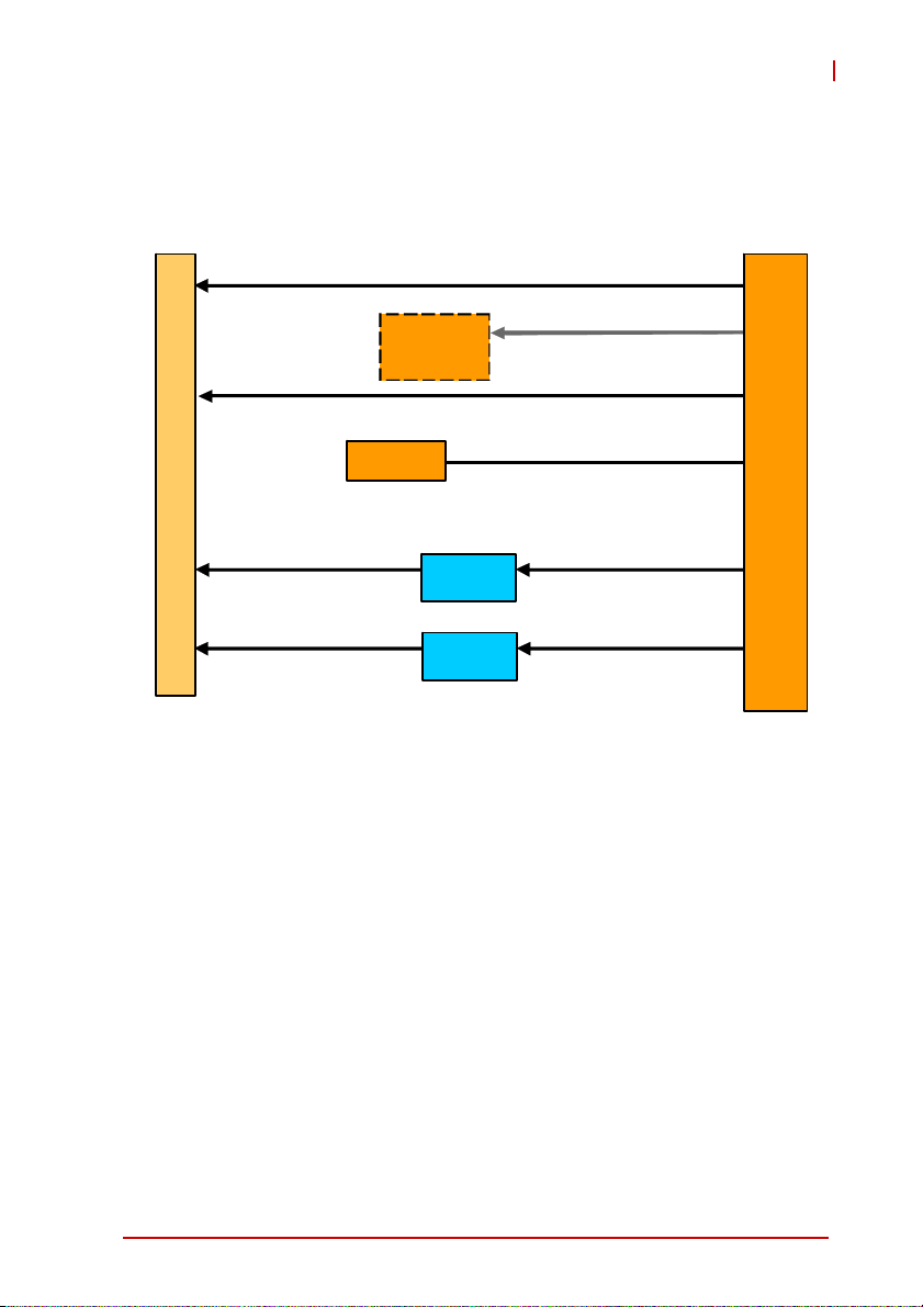
Figure 2-1: cPCI-3510 Blade Functional Block Diagram
12 Specifications
Page 27
DB-3610L2 Daughter Board
L2
F
r
o
n
t
P
a
n
e
l
PS/2, KB/MS
USB x2
Line-in, Line-out
2.5” HDD/SDD
COM
Codec
SATA0
Figure 2-2: DB-3610L2 Daughter Board Functional Block Diagram
B2B
Conn.
1
cPCI-3510
Specifications 13
Page 28
DB-3970L2 Daughter Board
L2
USB
F
r
o
DVI/DP
n
t
P
DVI/DP
a
n
e
l
2.5” HDD/SSD
B2B
Conn.
1/2
SATA0
COM1
10-pin
COM2
KB/MS
Figure 2-3: DB-3970L2 Daughter Board Functional Block Diagram
14 Specifications
Page 29
DB-LANL2-S Daughter Board
(cPCI-3510L versions)
USB x1
L2
F
R
RS232/422/485
O
N
T
P
A
N
E
GbE 3
L
Horizontal
Type A
2.5” HDD
82574L
cPCI-3510
B2B
Conn.
USB x1
SATA0
GbE 4
82574L
Figure 2-4: DB-LANL2-S Daughter Board Functional Bl ock Diagram
Specifications 15
Page 30
DB-Max Daughter Board
(cPCI-3510M versions)
100-pin
high
density
connector
F
R
O
N
T
P
A
N
E
L
Line-in, Line-out
2x DVI/DP
2.5” HDD/Slim
SSD
2x USB 2.0
2x COM (RS232/422/485)
KB/MS
SATA0
Figure 2-5: DB-Max Daught er Bo ard Functional Block Diagram
B2B
Conn.
16 Specifications
Page 31

cPCI-R3P00 RTM
cPCI-3510
J2
USB3
SATA3/4/5
FT232R
7 pin
COM (Tx, Rx)
2x USB
GbE 1/2
VGA
7 pin
7 pin
RS232/422/485
R
e
a
r
P
a
n
e
l
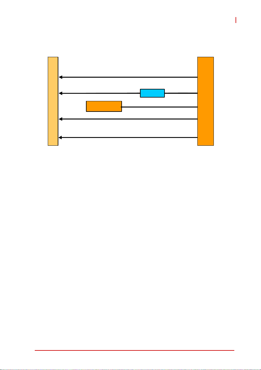
Figure 2-6: cPCI-R3P00 RTM Functional Block Diagram
Specifications 17
Page 32

cPCI-R3P00T RTM
J2
PCIe x4
SATA3/4/5
USB3 RS232/422/485
82580DB
7 pin
FT232R
7 pin
7 pin
COM (Tx, Rx)
2x USB
GbE 3/4
VGA
R
e
a
r
P
a
n
e
l
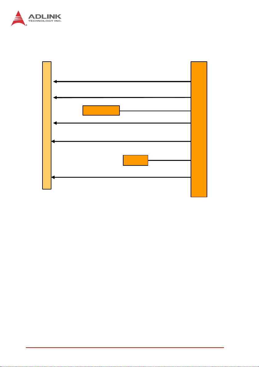
Figure 2-7: cPCI-R3P00T RTM Functional Block Diagram
18 Specifications
Page 33

2.4 I/O Connectivity Table
cPCI-3510
Function
cPCI-3510 (4HP) cPCI-3510D (8HP) cPCI-3510G (8HP)
Faceplate Onboard Faceplate Onboard Faceplate Onboard
Gigabit Ethernet Y x2 Y x2 Y x2
COM Y (DB-9) Y (RJ-45) Y (10-pin)
USB 3.0 Yx1 Yx1 Yx1
USB 2.0 Y x2 Y x1
DVI-I YYY
VGA
DisplayPort Y x2
Serial ATA Y ( for
2.5” drive)
CFast YYY
PS/2 KB/MS YY
Line-in/out Y
System LEDs Y x5 Y x5 Y x5
Reset Button YYY
Y ( for
2.5” drive)
Table 2-3: cPCI-3510 I/O Connectivity
Specifications 19
Page 34

Function
Gigabit Ethernet
COM Y (DB-9) Yx2 Y x2
USB 3.0 Yx1 Yx1
USB 2.0 Yx1 Y2x Y x2
DVI-I YY
VGA
DisplayPort
Serial ATA Y ( for
CFast YY
PS/2 KB/MS Y
Line-in/out Y
System LEDs Y x5 Y x5
Reset Button YY
cPCI-3510L (8HP) cPCI-3510M (8HP) R3P00(T) (RTM)
Faceplate Onboard Faceplate Onboard Faceplate Onboard
Yx4 Yx2
2.5” drive)
Y ( for
2.5” drive)
Y x2
Y
(1)
(2)
(7-pin)
Table 2-3: cPCI-3510 I/O Connectivity (cont’d)
1. Routed from CPU blade front ports for cPCI-R3P00, port s independent from front panel for cPCI-R3P00T.
2. VGA switched from front panel.
Y x3
20 Specifications
Page 35

cPCI-3510
2.5 Power Requirements
In order to guarantee a stable functionality of the system, it is recommended to provide more power than the system requires. An
industrial power supply unit should be able to provide at least
twice as much power as the entire system requires of each
voltage. An ATX power supply unit should be able to provide at
least three times as much power as the entire system requires of
each voltage.
The tolerance of the voltage lines described in the CompactPCI
specification (PICMG 2.0 R3.0) is +5%/-3% for 5, 3. 3 V and ±5%
for ±12V. This specification is for power delivered to each slot and
it includes both the power supply and the backplane tolerance.
Voltage
5V +5.0 VDC +5% / -3% 50 mV
3.3V +3.3 VDC +5% / -3% 50 mV
+12V +12 VDC +5% / -5% 240 mV
-12V -12 VDC +5% / -5% 240 mV
V I/O (PCI I/O
Buffer Voltage)
GND
Nominal
Value
+3.3 VDC or
+5 VDC
Tolerance
+5% / -3% 50 mV
Max. Ripple
(P - P)
Specifications 21
Page 36
Power Consumption
This section provides information on the power consumption of
cPCI-3510 Series when using the Intel® Core™ i7 processors with
4GB DDR3L-1600 ECC soldered memory and onboard 64GB SATA
flash disk. The cPCI-3510 is powered by 5V and 3.3V. Power consumption at 100% CPU usage was measured using the Intel Thermal Analysis Tool (TA T).
Intel® Core™i7-4700EQ
OS/Mode Current 5V Current 3.3V Total Power
DOS/Idle mode 3.79 A 0.73 A 21.4 W
Windows XP/Idle mode 3.56 A 0.71 A 20.1 W
Windows® XP, CPU 100% Usage 6.97 A 0.71 A 37.2 W
22 Specifications
Page 37

3 Functional Description
The following sections describe the cPCI-3510 Series features
and functions.
3.1 Processors
The Mobile 4th Generation Intel® Core™ Processor Family are state
of the art, 64-bit, multi-core mobile processor built on 22 nanometer
process technology. Based on a new micro-architecture, the processor is designed for a two-chip platform. The two-chip platform consists of a processor and Platform Controller Hub (PCH). The platform
enables higher performance, lower cost, easier validation, and
improved x-y footprint. The processor includes an Integrated Display
Engine, Processor Graphics and Integrated Memory Controller.
The cPCI-3510 Series supports Intel® Core™ i7/i5 processors. The
table below lists the general specifications and power ratings of
the CPUs supported by the
cPCI-3510 Series
.
cPCI-3510
Features
Clock 2.4GHz 2.7GHz 1.6 GHz
Max. Single Core
Turbo Freq.
Last Level Cache 6MB 3MB 3MB
No. of Core(s) 4/8 2/4 2/4
Max. Power (TDP1)
DMI
T
junction, MAX
1. The high est expected sustainable power while running known
2. The maximum supported operating temperature.
Functional Description 23
2
power intensive applications. TDP is not the maximum power
that the processor can dissipate.
Core™ i7-
4700EQ
3.4GHz - -
47W 37W 25W
5 GT/s 5 GT/s 5 GT/s
100°C 100°C 100°C
Core™ i5-
I5-4400E
Core™ i5-
4402E
Page 38
Supported Technologies
Features
Intel® Virtualization Technology
for Directed I/O (Intel® VT-d)
Intel® Virtualization Technology
(Intel® VT-x)
Intel® VT-x with Extended Page
Tables (EPT)
Intel® Hyper-Threading
Technology
Intel® 64 Architecture Yes Yes Yes
Execute Disable Bit Yes Yes Yes
Intel® Turbo Boost Technology 2.0 Yes Yes
Intel® vPro Technology Yes Yes Yes
Enhanced Intel SpeedStep®
Technology
Thermal Monitoring
Technologies
Intel® Identity Protection
Technology
Core™ i7-
4700EQ
Yes Yes Yes
Yes Yes Yes
Yes — —
Yes Yes Yes
Yes Yes Yes
Yes Yes Yes
Yes — —
Core™ i5-
I5-4400E
Core™ i5-
4402E
Interfaces
X Two channels of DDR3L-1333/1600 memory
X DDR3 memory data transfer rates of 1333 MT/s and 1600
MT/s
X 64-bit wide channels
X DDR3L I/O voltage of 1.35V
X 2Gb and 4Gb DDR3 DRAM technologies are supported for
x8 and x16 devices (using 4Gb device technologies, the
largest memory capacity possible is 8 GB, assuming
dual-channel mode with x8, dual-ranked ECC SDRAM)
X PCI Express ports are fully-compliant with the PCI Express
Base Specification, Revision 2.0.
X 5 GT/s point-to-point DMI interface to PCH is supported
24 Functional Description
Page 39

cPCI-3510
3.2 Platform Controller Hub
The Mobile Intel® QM87 Express Chipset provides extensive I/O
support. Functions and capabilities include:
X The QM87 PCH provides extensive I/O support, functions
and capabilities including:
X PCI Express Base Specification, Revision 2.0 support for up
to eight ports with transfers up to 5 GT/s
X ACPI Power Management Logic Support, Revision 4.0a
X Enhanced DMA controller, interrupt controller, and timer
functions
X Integrated Serial ATA host controllers with independent
DMA operation on up to six ports
X USB host interface with two EHCI high-speed USB 2.0 Host
controllers and two rate matching hubs provide support for
up to fourteen USB 2.0 ports
X Integrated 10/100/1000 Gigabit Ethernet MAC with System
Defense
X System Management Bus (SMBus) Specification, Version
2.0 with additional support for I2C devices
X Supports Intel® High Definition Audio
X Supports Intel® Rapid Storage Technology
X Supports Intel® Virtualization Technology for Directed I/O
X Integrated Clock Controller
X Analog and Digital Display ports
X Low Pin Count (LPC) interface
X Firmware Hub (FWH) interface support
X Serial Peripheral Interface (SPI) support
3.3 PMC/XMC
The cPCI-3510P/S/T models support one PMC or XMC site for
front panel I/O expansion. The PMC site provides a maximum
32-bit/66MHz PCI bus link using a Pericom PI7C9X130
PCI-Express-to-PCI bridge and PCI-Express x1 link. The PMC site
supports +3.3V signaling only. The XMC site provides a PCI
Express x1 lane.
Functional Description 25
Page 40

3.4 Intel® Turbo Boost Technology
Intel® Turbo Boost Technology is a feature that allows the pr ocessor to opportunistically and automatically run faster than its rated
operating core and/or render clock frequency when there is sufficient power headroom, and the product is within specified temperature and current limits. The Intel Turbo Boost Technology feature
is designed to increase performance of both multi-threaded and
single-threaded workloads. The processor supports a Turbo mode
where the processor can use the thermal capacity associated with
package and run at power levels higher than TDP power for
short durations. This improves the system responsiveness for
short, bursty usage conditions.
Turbo Mode availability is independent of the number of active
cores; however, the Turbo Mode frequency is dynamic and dependent on the instantaneous application power load, the number of
active cores, user configurable settings, operating environment,
and system design. If the power, current, or thermal limit is
reached, the processor will automatically reduce the frequency to
stay with its TDP limit.
3.5 Intel® Hyper-Threading Technology
Intel® Hyper-Threading Technology allows an execution core to
function as two logical processors. While some execution
resources (such as caches, execution units, and buses) are
shared, each logical processor has its own architectura l state with
its own set of general-purpose registers and control registers. This
feature must be enabled using the BIOS and requires operating
system support. Intel recommends enabling Hyper-Threading
Technology with Microsoft Windows 7, Vista, and XP, and disabling Hyper-Threading Technology using the BIOS for all prev ious versions of Windows operating systems.
3.6 Trusted Plat form Module
The cPCI-6530 is optionally equipped with an Atmel AT97SC3204
Trusted Platform Module (TPM). The TPM is a secure controller
with added cryptographic functionality to provide users a secure
environment in e-commerce transactions and Internet communications.
26 Functional Description
Page 41

The key features Trusted Platform Module (TPM) offers are:
X Fully compliant to the Trusted Computin g Group (TCG)
Trusted Platform Module (TPM) version 1.2 specification
X Hardware hash accelerator for SHA-1 algorithm
X Advanced Crypto Engine (ACE) for asymmetric key opera-
tions(up to 2048-bit key length) to make hardware protection.
X Tick counter to extend the time required to decipher the key
X In addition to encryption key created by user . it also provide
some security features to protect the integrated circuit itself:
X Over/Under-voltage detection to monitor the system stabil-
ity. If the voltage fluctuates dramatically, this function can
block the data transfer and lock the chip.
X Low/High frequency sensor to detect the IC clock fre-
quency. If the frequency fluctuates dramatically, this function can block the data transfer and lock the chip.
X Reset filter to filter reset signal in order to break the time se t
by tick counter is received
X Memory encryption to protect memory
X Physical shield in the IC to protect the die from intruding or
hacking by matching the data transferred on the 2 layer
metal shield on the IC. If the data is not matched, the IC
may be blocked.
cPCI-3510
3.7 Battery
The cPCI-3510 is equipped with a 3.0V "coin cell" lithium battery
for the Real Time Clock (RTC). The battery socket is equipped on
the DB-3CFAST daughter board. The lithium battery must be
replaced with an identical battery or a battery type recommended
by the manufacturer. A Rayovac BR2032 is equipped on board by
default, and can be optionally equipped with a Gold Capacitor
(Panasonic EECS5R5H105).
Functional Description 27
Page 42

This page intentionally left blank.
28 Functional Description
Page 43

4 Board Interfaces
This chapter illustrates the board layout, connector pin
assignments, and jumper settings to familiarize users with the
cPCI-3510 Series.
4.1 cPCI-3510 Series Board Layout
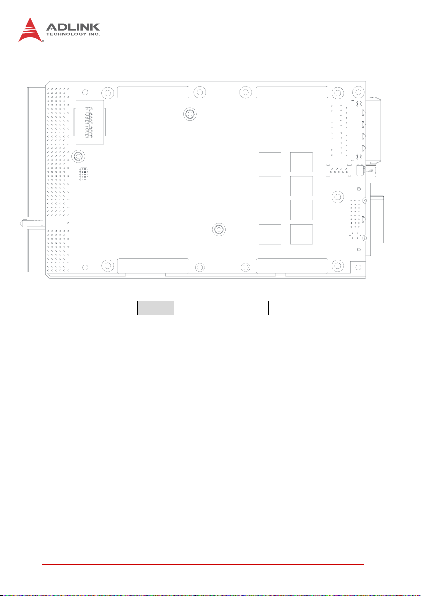
cPCI-3510
LAN1
DVI1
USB1
CN1
CN3
CPU1
CN2
PCH
U2201
CPU Intel® Core™ Processor J1 CompactPCI Connector J1
PCH Intel® QM87 PCH J2 cPCI J2 (UHM/HM)
CN4/5 Stacked SO-CDIMM socket LAN1 Dual Ethernet connectors
CN1 DB-3610L2/DB-3970L2
DVI1 DVI connector
connector
CN2 DB-3CFAST connector USB1 USB port
CN3 DB-3970L2 connector U2201 Pericom PI7C9X130
Figure 4-1: cPCI-3510 Series Board Layout (component side)
J2
J1
Board Interfaces 29
Page 44
SW1 Reset Button
Figure 4-2: cPCI-3510 Series Board Layout (solder side)
SW1
30 Board Interfaces
Page 45

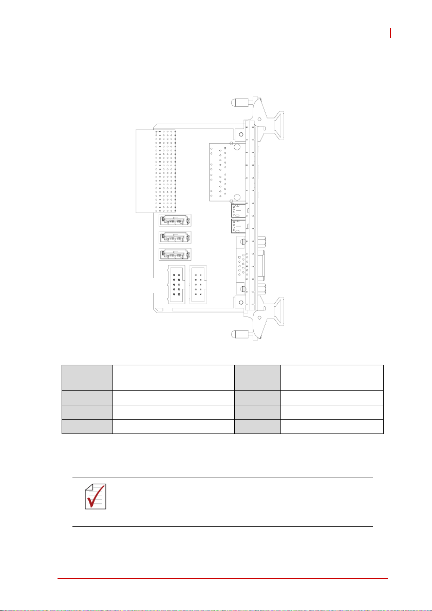
cPCI-3510
4.2 cPCI-3510 Blade Assembly Layout
This section describes the final assembly layout of the single slot
cPCI-3510 Blade.
BT1
J2
JP1
Heatsink
CFast
DB-3CFAST
Figure 4-3: cPCI-3510 Blade Assembly Layout
BT1 Battery CFast CFast socket
JP1 Clear CMOS Jumper J2 cPCI J2 (UHM/HM)
Board Interfaces 31
Page 46

4.3 cPCI-3510D Blade Assembly Layout
S
The dual-slot width cPCI-3510D Blade is comprised of the
cPCI-3510 single-slot main board and the DB-3610L2 riser card to
expand I/O connectivity with PS/2, COM, 2x USB ports, Line-in,
and Line-out ports .
COM1
USB2
USB3
PS/2
CN6
CN8
ATA0
2.5” SATA HDD
CN7
COM1 DB-9 COM port CN7 DB-3UMC connector
USB2/3 USB connectors CN6 Line-in port
PS2 PS/2 KB/Ms Combo port CN8 Line-out port
SATA0 22-pin SATA connector
Figure 4-4: cPCI-3510D Blade Assembly Layout
DB-3610L2
32 Board Interfaces
Page 47

cPCI-3510
4.4 cPCI-3510G Blade Assembly Layout
The dual-slot width cPCI-3510G Blade is comprised of the
cPCI-3510 single-slot main board and the DB-3970L 2 ri ser card to
expand I/O connectivity with PS/2, COM, USB ports, and 2x DisplayPorts.
CN2
COM2
SATA0
2.5” SATA HDD
DP1
DP2
COM1
PS2
USB9
COM1 RJ-45 COM port CN2 DB-3UMC connector
COM2 10-pin COM port DP1/2 DisplayPort connectors
USB9 USB connector PS2 PS/2 KB/MS Combo port
SATA0 22-pin SATA connector
Figure 4-5: cPCI-3510G Blade Assembly Layout
DB-3970L2
Board Interfaces 33
Page 48

4.5 cPCI-3510L Blade Assembly Layout
The dual-slot width cPCI-3510L Blade is comprised of the
cPCI-3510 single-slot main board and the DB-LAN2-S daughter
board, expanding I/O connectivity with 2x LAN, COM, USB.
LAN1
2.5” SATA HDD SATA1
COM1
USB1
DB-LAN2-S
LAN1 GbE RJ-45 ports USB1 USB connector
COM1 DB-9 COM port SATA1 22-pin SATA connector
Figure 4-6: cPCI-3510L Blade Assembly Layout
34 Board Interfaces
Page 49

cPCI-3510
4.6 cPCI-3510M Blade Assembly Layout
The dual-slot width cPCI-3510M Blade is comprised of the
cPCI-3510 single-slot main board and the DB-Max daughter
board, expanding I/O connectivity with a 100-pin high density connector.
CN4
CN4 100-pin high density
connector
Figure 4-7: cPCI-3510M Blade Assembly Layout
SATA0
DB-Max
SATA0 22 -pin SATA connector
Board Interfaces 35
Page 50
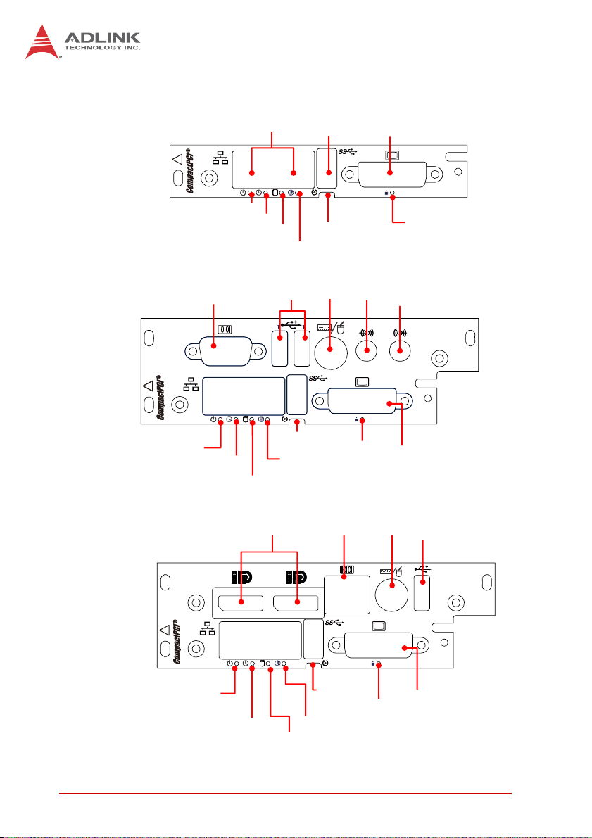
4.7 cPCI-3510, cPCI-3510D, cPCI-3510G Faceplate
cPCI-3510
cPCI-3510D
cPCI-3510G
Power LED
AB
Power LED
WDT LED
HDD LED
Thermal LED
COM1
AB
WDT LED
HDD LED
DisplayPorts
GbE A/B
USB 2.0
USB .0
Reset Button
PS/2
KB/MS
Reset Button
Thermal LED
COM1
Line-in
GP LED
DVI
Line-out
DVI-I
PS/2
KB/MS
GP LED
USB 2.0
AB
Power LED
WDT LED
HDD LED
Reset Button
Thermal LED
GP LED
DVI-I
Figure 4-8: cPCI-3510, cPCI-3510D, cPCI-3510G Front Panel Layout
36 Board Interfaces
Page 51

4.8 cPCI-3510L, cPCI-3510M Front Panel
cPCI-3510L
cPCI-3510
cPCI-3510M
LAN Connector
CD
AB
Power LED
WDT LED
AB
Thermal LED
HDD LED
COM
GP LED
100-pin connector
DVI-I
Power LED
WDT LED
HDD LED
Reset Button
Thermal LED
GP LED
DVI-I
Figure 4-9: cPCI-3510L, cPCI-3510M Front Panel Layout
Board Interfaces 37
Page 52

System LEDs
LED Color Condition Indication
Power1
1
WDT
Green/
Red
Orange
OFF System is of f
Red System Power ready (PWGD)
Green Post OK
OFF No Watchdog event
Blinking Watchdog event alert
HDD
Overheat
Blue
1
Red
OFF N o CFast/ SATA HDD activity
Blinking
OFF
ON
Data read/write in process for CF/CFast/
SATA HDD
CPU T
CPU T
temperature is under 100ºC
junction
temperature exceeds 100ºC
junction
GP
(General
Purpose)
1
Yellow
OFF N o activity
ON/Blinking Defined by user
Table 4-1: cPCI-3510 Front Panel System LED Descriptions
1. Power, WDT, Overheat, GP LEDs are connected to GPIO pins
of IPMC. The Power, WDT, Thermal LEDs can be programmed
by the user as general purpose LEDs.
38 Board Interfaces
Page 53
4.9 cPCI-R3P00(T) RTM Board Layout
cPCI-3510
rJ2
SATA2
SATA4
SATA3
COM4
COM5* RS-232/422/485 port
COM5
LAN1/2
USB1
USB10
VGA1
LAN1/2 Dual Ethernet ports
(converted from USB)
COM4 RS-232 port (Tx, Rx only) VGA1 VGA port
SATA2/3/4 SATA ports USB1/10 USB ports
rJ2 CompactPCI connector
(cPCI-R3P00 is 50mm deep and cPCI-R3P00T is 80mm deep)
Figure 4-10: cPCI-R3P00(T) RTM Board Layout
*COM5 is incorrectly labeled COM3 on the A1 vers. PCB
silkscreen.
NOTE:
NOTE:
Board Interfaces 39
Page 54
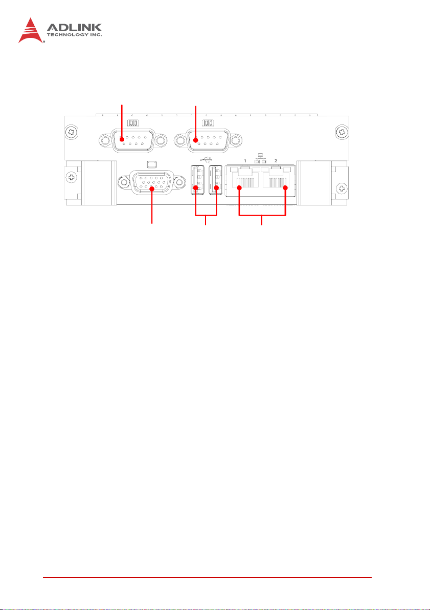
4.10 cPCI-R3P00(T) RTM Faceplate
COM4 COM5
VGA
USBx2 GbE x2
Figure 4-11: cPCI-R3P00(T) RTM Front Panel
40 Board Interfaces
Page 55
4.11 Connector Pin Assignments
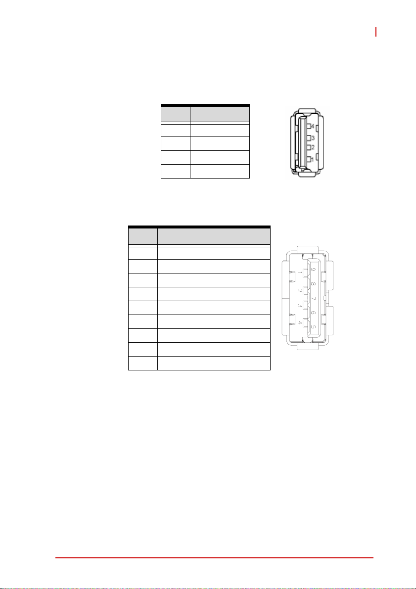
USB 2.0 Connectors
cPCI-3510
Pin # Signal Name
Table 4-2: USB 2.0 Pin Definition
USB 3.0 Connectors
Pin # Signal Name
1 USB3.0_P5VA
2 USB2_CMAN
3 USB2_CMAP
4GND
5 USB3A_CMRXN
6 USB3A_CMRXP
7GND
8 USB3A_CMTXN
9USB3A_CMTXP
1Vcc
2UV03UV0+
4GND
Board Interfaces 41
Page 56
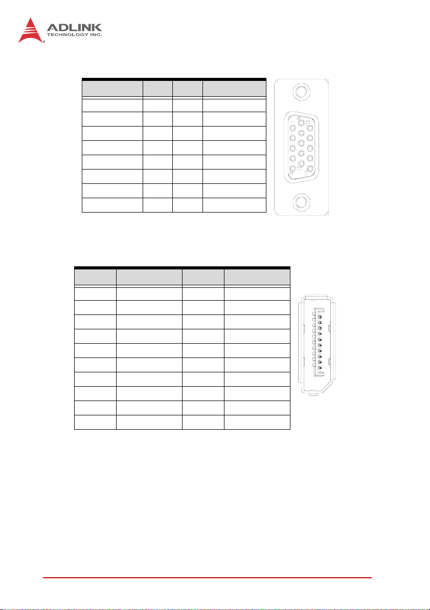
DB-15 VGA Connector
Signal Name Pin # Pin # Signal Name
Red 1 2 Green
Blue 3 4 N.C.
GND 5 6 GND
GND 7 8 GND
+5V. 9 10 GND
N.C. 11 12 CRTDATA
HSYNC 13 14 VSYNC
CRTCLK 15
Table 4-3: VGA Pin Definition
DisplayPort Connectors
Pin # Signal Pin # Signal
1 CN_DP0_P 2 Ground
3 CN_DP0_N 4 CN_DP1_P
5 Ground 6 CN_DP1_N
7 CN_DP2_P 8 Ground
9 CN_DP2_N 10 CN_DP3_P
11 Ground 12 CN_DP3_N
13 CN_CAD-L 14 CN_CEC
15 CN_AUX_P 16 Ground
17 CN_AUX_N 18 DDP_HPD
19 Ground 20 P3V3
1
2
19
20
Table 4-4: DisplayPort Pin Definition
42 Board Interfaces
Page 57

DVI-I Connector
Pin # Signal Pin # Signal
1 TMDS Data2- 16 Hot Plug Detect
2 TMDS Data2+ 17 TMDS Data03 GND 18 TMDSData0+
4NC19GND
5NC20NC
6 DDC Clock [SCL] 21 NC
7 DDC Data [SDA] 22 GND
8 Analog vertical sync 23 TMDS Clock +
9 TMDS Data1- 24 TMDS Clock 10 TMDS Data1+ C1 Analog Red
11 GND C2 Analog Green
12 NC C3 Analog Blue
13 NC C4 Analog Horizontal Sync
14 +5 V Power C5 Analog GND Return
15 GND
cPCI-3510
T able 4-5: DVI-I Connector Pin Definition
Board Interfaces 43
Page 58

RJ-45 Gigabit Ethernet Connectors
Pin #
10BASE-T/
100BASE-TX
1 TX+ LAN_TX0+
2 TX- LAN_TX03 RX+ LAN_TX1+
4 — LAN_TX2+
5 — LAN_TX26 RX- LAN_TX17 — LAN_TX3+
8 — LAN_TX3-
Table 4-6: RJ-45 GbE Pin Definitions
Speed
Status
Network link is not established
or system powered off
10 Mbps
100 Mbps
1000 Mbps
Link OFF ON
Active OFF Blinking
Link Green ON
Active Green Blinking
Link Orange ON
Active Orange Blinking
1000BASE-T
Activity
18
Speed LED
(Green/Orange)
OFF OFF
Activity LED
(Yellow)
Table 4-7: LAN LED Status Definitions
The cPCI-R3P00 RTM LAN LED signals are not passed
through from the main board and are not displayed on the front
NOTE:
NOTE:
panel LAN LEDs.
44 Board Interfaces
Page 59

PS/2 Keyboard/Mouse Connector
Pin # Signal Function
1 KBDATA Keyboard Data
2MSDATA Mouse Data
3 GND Ground
4+5V Power
5 KBCLK Keyboard Clock
6 MSCLK Mouse Clock
Table 4-8: PS/2 Keyboard/Mouse Pin Definition
cPCI-3510D/P Serial Ports
COM1 Connector (DB-9)
Pin # RS-232 RS-422 RS-485(+)
1 DCD-L TXD- TXD2RXDTXD+TXD+
3TXDRXD+ —
4 DTR-L RXD- —
5 GND GND GND
6DSR-L — —
7RTS-L — —
8CTS-L — —
9RI-L — —
cPCI-3510
Table 4-9: cPCI-3510D/P COM1 (DB-9) Pin Definition
The COM mode setting for cPCI-3510D/P models is set using
SW1~SW4. See “COM1 Mode Selection Switches
NOTE:
NOTE:
(SW1~SW4)” on page 46.
Board Interfaces 45
Page 60
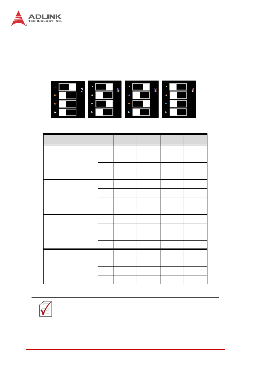
COM1 Mode Selection Switches (SW1~SW4)
These switches set the cPCI-3510D/P COM1 to RS-232 full
modem, RS-422, RS-485, or RS-485+ half-duplex mode.
Switches SW1~SW4 are located on the top edge of the
DB-3610L2 board. RS-232 full modem is set by default.
SW1 S W2 SW3 SW4
Mode Pin SW1 SW2 SW3 SW4
1ONONONOFF
RS-232
RS-422
RS-485
RS-485+
2 OFF OFF OFF OFF
3 OFF ON ON OFF
4 OFF OFF OFF OFF
1 OFF OFF OFF ON
2ONONONOFF
3 OFF OFF OFF ON
4 OFF ON ON OFF
1 OFF OFF OFF ON
2 OFF ON ON OFF
3ONOFFOFFON
4 OFF ON ON OFF
1 OFF OFF OFF OFF
2 OFF ON ON ON
3ONOFFOFFOFF
4 OFF ON ON ON
T able 4-10: cPCI-3510D/P COM1 Mode Selection Switch Settings
The COM mode setting for cPCI-3510D/P models must be set
using the SW1~SW4 DIP switches above. The cPCI-3510G/T
NOTE:
NOTE:
COM1/2 Output BIOS setting is only used for cPCI-3510G/T
models.
46 Board Interfaces
Page 61

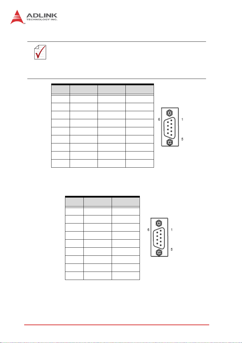
cPCI-3510G/T Serial Ports
COM1 Connector (RJ-45)
Pin # RS-232 RS-422 RS-485
1DCD-L — —
2 RTS-L TXD+ TXD+
3DSR-L — —
4 TXD TXD- TXD5 RXD RXD- —
6 Ground — —
7CTS-LRXD+ —
8DTR-L — —
9RI-L — —
Table 4-11: cPCI-3510G/T COM1 (RJ-45) Pin Definition
The COM mode settings for cPCI-3510G/T models are set in
the BIOS: see “Output (cPCI-3510G/T COM1/2)” on page 104.
NOTE:
NOTE:
cPCI-3510
COM1 Connector with DB-9 Adapter
An RJ-45 to DB-9 adapter cable is provided to breakout the
COM1 signals.
Pin # RS-232 RS-422 RS-485
1DCD-L — —
2 RXD RXD- —
3 TXD TXD- TXD4DSR-L — —
5 Ground — —
6DSR-L — —
7 RTS-L TXD+ TXD+
8CTS-LRXD+ —
9— — —
Table 4-12: cPCI-3510G/T COM1 (DB-9 adapter) Pin Definition
Board Interfaces 47
Page 62

The cPCI-3510G/T COM1 RS-422/485 pin definitions are different from the common DB-9 pin definitions. An RS-422/485 DB-9
NOTE:
NOTE:
male-female adapter dongle is provided to allow compatibility
with common RS-422/485 pin definitions.
RS-422/485 Adapter Dongle for cPCI-3510G/T
A DB-9 male-female adapter dongle is provided to allow compatibility with common RS-422/485 pin definitions
DB-9 (Female)
Signal Name
Pin #
DB-9 (Male)
Signal Name
NC 1 TXD-
RXD- 2 TXD+
TXD- 3 RXD+
NC 4 RXDNC 5 NC
NC 6 NC
TXD+ 7 NC
RXD+ 8 NC
NC 9 NC
Table 4-13: RS-422/485 Adapter Dongle Pin Definition
COM1 with RS-422/485 Dongle (DB-9)
Pin # RS-422 RS-485
1TXD-TXD2 TXD+ TXD+
3RXD+ —
4RXD- —
5— —
6— —
7— —
8— —
9— —
Table 4-14: cPCI-3510G/T COM1 with RS-422/485 Dongle Pin Definition
48 Board Interfaces
Page 63

COM2 Pin Header
Pin # RS-232 RS-422 RS-485
1DCD-L — —
2DSR-L — —
3 RXD RXD- —
4 RTS-L TXD+ TXD+
5 TXD TXD- TXD6CTS-LRXD+ —
7DTR-L — —
8RI-L — —
9 Ground — —
10 NC — —
Table 4-15: cPCI-3510G/T COM2 Pin Header Definition
The COM mode settings for cPCI-3510G/T models are set in
the BIOS: see “Output (cPCI-3510G/T COM1/2)” on page 104.
NOTE:
NOTE:
cPCI-3510
12
910
cPCI-R3P00(T) RTM Serial Ports
COM4 Connector (DB-9))
Pin # RS-232
1—
2RXD
3TXD
4—
5GND
6—
7—
8—
9—
Ta ble 4-16: cPCI-R3P00 RTM COM4 Pin Definition
Board Interfaces 49
Page 64
COM5 Connector (DB-9)
The cPCI-R3P00(T) RTM COM5 RS-422/485 pin definitions are
different from the common DB-9 pin definitions. An RS-422/485
NOTE:
NOTE:
DB-9 male-female adapter dongle is provided to allow compatibility with common RS-422/485 pin definitions. See “RS-422/485
Adapter Dongle for cPCI-3510G/T” on page 48
Pin # RS-232 RS-422 RS-485
1 DCD-L — —
2 RXD RXD- —
3 TXD TXD- TXD4DTR-L — —
5GND — —
6DSR-L — —
7 RTS-L TXD+ TXD+
8 CTS-L RXD+ —
9RI-L — —
Table 4-17: cPCI-R3P00(T) RTM COM5 Pin Definition
COM5 with RS-422/485 Dongle (DB-9)
Pin # RS-422 RS-485
1TXD-TXD2 TXD+ TXD+
3RXD+ —
4RXD- —
5— —
6— —
7— —
8— —
9— —
Table 4-18: cPCI-R3P00(T) RTM COM5 with RS-422/485 Dongle Pin Def’n
50 Board Interfaces
Page 65

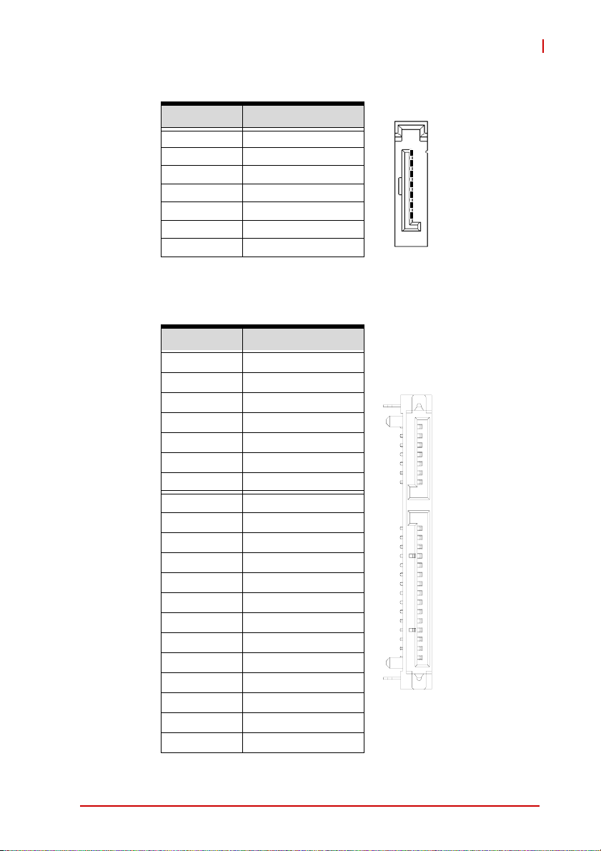
cPCI-3510M 100-pin I/O Connector (CN4)
Pin # Signal Pin # Signal
1 GND 2 USB9_CN-N
3 USB9_CN-P 4 GND
5 USB1_CN-N 6 USB1_CN-P
7 GND 8 GND
9 TMDS_I2C_DATA 10 TMDS_I2C_CLK
11 GND 12 TMDSB_DATA2B
13 TMDSB_DAT A2 14 GND
15 TMDSB_DATA1B 16 TMDSB_DATA1
17 GND 18 TMDSB_DATA0B
19 TMDSB_DAT A0 20 GND
21 TMDSB_CLKB 22 TMDSB_CLK
23 GND 24 P5V_DVI1
25 TMDSB_HPD 26 GND
27
NC
29 GND 30 TMDS_I2C_DATA
31 TMDS_I2C_CLK 32 GND
33 TMDSB_DATA2B 34 TMDSB_DATA2
35 GND 36 TMDSB_DATA1B
37 TMDSB_DAT A1 38 GND
39 TMDSB_DATA0B 40 TMDSB_DATA0
41 GND 42 TMDSB_CLKB
43 TMDSB_CLK 44 GND
45 P5V_DVI2 46 TMDSB_HPD
47 GND 48 NC
49 NC 50 GND
51 P5V_USB_1_9 52 P5V_USB_1_9
53 P5V_USB_1_9 54 P5V_USB_1_9
55 GND 56 GND
57 GND 58 P5V_KBMS
59 MSCLK_CN 60 MSDATA_CN
Table 4-19: cPCI-3510M 100-pin I/O Connector Pin Definition
28 NC
cPCI-3510
1
99
2
100
Board Interfaces 51
Page 66

Pin # Signal Pin # Signal
61 KBCLK_CN 62 KBDATA_CN
63 GND 64 GND
65 COM1_RXD_CN 66 COM1_CTS-L_CN
67 GND 68 COM1_TXD_CN
69 COM1_RTS-L_CN 70 GND
71 COM1_DTR-L_CN 72 COM1_DSR-L_CN
73 COM1_DCD-L_CN 74 GND
75 COM2_RXD_CN 76 COM2_CTS-L_CN
77 GND 78 COM2_TXD_CN
79 COM2_RTS-L_CN 80 GND
81 COM2_DTR-L_CN 82 COM2_DSR-L_CN
83 COM2_DCD-L_CN 84 AGND_AU
85 NC 86 NC
87 NC 88 NC
89 NC 90 NC
91 NC 92 AGND_AU
93 L_IN_R 94 L_IN_L
95 L_IN_JD 96 AGND_AU
97 HP_R 98 HP_L
99 HP_JD 100 AGND_AU
Table 4-19: cPCI-3510M 100-pin I/O Connector Pin Definition
52 Board Interfaces
Page 67
Serial ATA Connectors on RTM (CN4-R, CN5-R)
Pin # Signal
1GND
2TX+
1
3TX4GND
5RX-
7
6RX+
7GND
Table 4-20: Serial ATA Connector on RTM
Serial ATA Connector on DB-3610L2/3970L2
Pin # Signal
S1 GND
S2 TX+
S3 TXS4 GND
S5 RXS6 RX+
S7 GND
P1 NC
P2 NC
P3 NC
P4 GND
P5 GND
P6 GND
P7 5V
P8 5V
P9 5V
P10 GND
P11 NC
P12 GND
P13~P15 NC
cPCI-3510
S1
Signal
S7
P1
Power
P15
Table 4-21: Serial ATA Connector on DB-3610L2/3970L2 Pin Definition
Board Interfaces 53
Page 68
CFast Socket (on DB-3CFAST)
Pin # Signal Name
Ground S1
SATA_TX-P S2
SATA_TX-N S3
Ground S4
SATA_RX-N S5
SATA_RX-P S6
Ground S7
CFast_CDI P1
Ground P2
NC P3
NC P4
NC P5
NC P6
Ground P7
CFast_LED1 P8
CFast_LED2 P9
NC P10
NC P11
NC P12
P3V3 P13
P3V3 P14
Ground P15
Ground P16
CFast_CDO P17
24
1
S1P1
Table 4-22: CFast Socket Pin Definition
54 Board Interfaces
Page 69

DB-3610L2 Connector (CN1)
Signal Name Pin # Pin # Signal Name
USB2-N 1 2 -12V
USB2-P 3 4 +12
GND 5 6 GND
USB3-N 7 8 HDA_SDIN0
USB3-P 9 10 HDA_R_SDOUT
GND 11 12 GND
SATA_ICH_RX-N0 13 14 HDA_R_SYNC
SATA_ICH_RX-P0 15 16 HDA_R_BIT_CLK
GND 17 18 GND
SATA_TX-P0 19 20 CK_L2_PCIE1-P
SATA_TX-N0 21 22 CK_L2_PCIE1-N
GND 23 24 GND
PCIE_TXN5 25 26 CK_L2_PCIE2-P
PCIE_TXP5 27 28 CK_L2_PCIE2-N
GND 29 30 GND
PCIE_RXN5 31 32 HDA_R_RST-L
PCIE_RXP5 33 34 SPKR
GND 35 36 L2_PCIE_RST-L
PCIE_RXN4 37 38 NC
PCIE_RXP4 39 40 USB_2_3_OC-L
GND 41 42 COM1_DCD-L
PCIE_TXN4 43 44 COM1_RI-L
PCIE_TXP4 45 46 COM1_CTS-L
GND 47 48 COM1_DTR-L
MSCLK 49 50 COM1_RTS-L
MSDATA 51 52 COM1_DSR-L
KBCLK 53 54 COM1_SOUT
KBCDATA 55 56 COM1_SIN
P5V 57 58 +3.3V
P5V 59 60 +3.3V
Table 4-23: DB-3610L2 Connector Pin Definition
cPCI-3510
60
12
59
Board Interfaces 55
Page 70
DB-3CFAST Connector (CN2)
Signal Name Pin # Pin # Signal Name
PCH_SPKR 1 2 CLK33_TPM
SIO_SPKR 3 4 LPC_FRAME-L
GND 5 6 TPM_RST-L
CN_VCC_RTC 7 8 LPC_AD3
GND 9 10 LPC_AD2
NC 11 12 LPC_AD1
NC 13 14 LPC_AD0
NC 15 16 TPM_LPCPD
NC 17 18 PCH_SERIRQ
NC 19 20 TPM_CLKRUN
NC 21 22 TPM_GPIO
NC 23 24 NC
NC 25 26 NC
NC 27 28 NC
NC 29 30 NC
NC 31 32 NC
NC 33 34 NC
NC 35 36 NC
GND 37 38 NC
SATA_PCH_RX-N0 39 40 NC
SATA_PCH_RX-P0 41 42 NC
GND 43 44 NC
SATA_PCH_TX-N0 45 46 NC
SATA_PCH_TX-P0 47 48 NC
GND 49 50 NC
CFast_CDI 51 52 NC
CFast_CDO 53 54 NC
GND 55 56 NC
P5V 57 58 P3V3
P5V 59 60 P3V3
Table 4-24: DB-3CFAST Connector Pin Definition
60
12
59
56 Board Interfaces
Page 71

DB-3970L2 Connector (CN3)
Signal Name Pin # Pin # Signal Name
NC 1 2 RS232_COM2_SEL-L
NC 3 4 COM2_DCD-L
NC 5 6 COM2_RI-L
NC 7 8 COM2_CTS-L
NC 9 10 COM2_DTR-L
NC 11 12 COM2_RTS-L
NC 13 14 COM2_DSR-L
NC 15 16 COM2_SOUT
NC 17 18 COM2_SIN
NC 19 20 NC
NC 21 22 NC
GND 23 24 GND
PCH_DDPD_AUXN 25 26 PCH_DDPC_AUXN
PCH_DDPD_AUXP 27 28 PCH_DDPC_AUXP
GND 29 30 GND
PCH_DDPD_0N 31 32 PCH_DDPC_0N
PCH_DDPD_0P 33 34 PCH_DDPC_0P
GND 35 36 GND
PCH_DDPD_1N 37 38 PCH_DDPC_1N
PCH_DDPD_1P 39 40 PCH_DDPC_1P
GND 41 42 GND
PCH_DDPD_2N 43 44 PCH_DDPC_2N
PCH_DDPD_2P 45 46 PCH_DDPC_2P
GND 47 48 GND
PCH_DDPD_3N 49 50 PCH_DDPC_3N
PCH_DDPD_3P 51 52 PCH_DDPC_3P
GND 53 54 GND
DDPD_CTRLCLK 55 56 DDPC_CTRLCLK
DDPD_CTRLDATA 57 58 DDPC_CTRLDATA
DDPD_HPD 59 60 DDPC_HPD
Table 4-25: DB-3970L2 Connector Pin Definition
cPCI-3510
60
12
59
Board Interfaces 57
Page 72
DB-3UMC Connector on DB-3610L2/3970L2
Signal Name Pin # Pin # Signal Name
NC 1 2 -12V
NC 3 4 +12V
GND 5 6 GND
NC 7 8 NC
NC 9 10 NC
GND 11 12 GND
NC 13 14 NC
NC 15 16 NC
GND 17 18 GND
NC 19 20 CK_PCIE1_P
NC 21 22 CK_PCIE1_N
GND 23 24 GND
PCIE_TXN2 25 26 CK_PCIE2_P
PCIE_TXP2 27 28 CK_PCIE2_N
GND 29 30 GND
PCIE_R_RXN2 31 32 NC
PCIE_R_RXP2 33 34 NC
GND 35 36 PCIE_RST#
PCIE_R_RXN1 37 38 NC
PCIE_R_RXP1 39 40 NC
GND 41 42 NC
PCIE_TXN4 43 44 NC
PCIE_TXP4 45 46 NC
GND 47 48 NC
NC 49 50 NC
NC 51 52 NC
NC 53 54 NC
NC 55 56 NC
+5V 57 58 +3.3V
+5V 59 60 +3.3V
Table 4-26: DB-3UMC Connector Pin Definition
60
12
59
58 Board Interfaces
Page 73
PMC Connector on DB-3UMC (JN1/2)
cPCI-3510
Pin# JN1 Signal JN2 Signal
1 PMC_TCK P12V
2 N12V PMC_TRST-L
3 GND PMC_TMS
4 PCIX_INTA-L NC (PMC_TDO)
5 PCIX_INTB-L PMC_TDI
6PCIX_INTC-L GND
7PMC_MOD-L1 GND
8P5V NC
9 PCIX_INTD-L NC
10 NC NC
11 GND PMC_MOD-L2
12 P3V3_PMCAUX P3V3
13 CLK66_PCIX_PMC PMC_RST-L
14 GND PMC_MOD-L3
15 GND P3V3
16 PCIX_GNT-L0 PMC_MOD-L4
17 PCIX_REQ-L0 PMC_PME-L
18 P5V GND
19 PMC_VIO PCIX_AD30
20 PCIX_AD31 PCIX_AD29
21 PCIX_AD28 GND
22 PCIX_AD27 PCIX_AD26
23 PCIX_AD25 PCIX_AD24
24 GND PCIX_AD23
25 GND PMC_IDSEL
26 PCIX_CBE-L3 PCIX_AD23
27 PCIX_AD22 P3V3
28 PCIX_AD21 PCIX_AD20
29 PCIX_AD19 PCIX_AD18
30 P5V GND
31 PCIX_FRAME-L PCIX_AD1 6
32 PCIX_AD17 PCIX_CBE-L2
Table 4-27: PMC Connector Pin Definitions
6364
12
Board Interfaces 59
Page 74
Pin# JN1 Signal JN2 Signal
33 PCIX_FRAME-L GND
34 GND NC
35 GND PCIX_TRDY-L
36 PCIX_IRDY-L P3V3
37 PCIX_DEVSEL-L GND
38 P5V PCIX_STOP-L
39 PCIX_PCIXCAP PCIX_PERR-L
40 PCIX_LOCK-L GND
41 NC P3V3
42 NC PCIX_SERR-L
43 PCIX_PAR PCIX_CBE-L1
44 GND GND
45 PMC_VIO PCIX_AD14
46 PCIX_AD15 PCIX_AD13
47 PCIX_AD12 PCIX_M66EN
48 PCIX_AD11 PCIX_AD10
49 PCIX_AD9 PCIX_AD8
50 P5V P3V3
51 GND PCIX_AD7
52 PCIX_CBE-L0 NC
53 PCIX_AD6 P3V3
54 PCIX_AD5 NC
55 PCIX_AD4 NC
56 GND GND
57 PMC_VIO NC
58 PCIX_AD3 NC
59 PCIX_AD2 GND
60 PCIX_AD1 NC
61 PCIX_AD0 PCIX_ACK64-L
62 P5V P3V3
63 GND GND
64 PCIX_REQ64-L NC
Table 4-27: PMC Connector Pin Definition s (cont’d)
60 Board Interfaces
Page 75

cPCI-3510
XMC Connector on DB-3UMC (JN3)
Pin# A B C D E F
1RXP RXN 3.3V NC NC VPWR
2 GND GND Not used GND GND PCIE_RST-L
3NC NC 3.3V NC NC VPWR
4 GND GND Not used GND GND Not used
5NC NC 3.3V NC NC VPWR
6 GND GND Not used GND GND +12V
7NC NC 3.3V NC NC VPWR
8 GND GND Not used GND GND -12V
9 NC NC Not used NC NC VPWR
10 GND GND Not used GND GND GA0
11 TXP TXN Not used NC NC VPWR
12 GND GND GA1 GND GND Not used
13 NC NC 3.3V NC NC VPWR
14 GND GND GA2 GND GND Not used
15 NC NC Not used NC NC VPWR
16 GND GND Not used GND GND Not used
17 NC NC Not used NC NC NC
18 GND GND Not used GND GND Not used
19 CK-P CK-N Not used Not used Not used Not used
Table 4-28: XMC Connector Pin Definition
Board Interfaces 61
Page 76

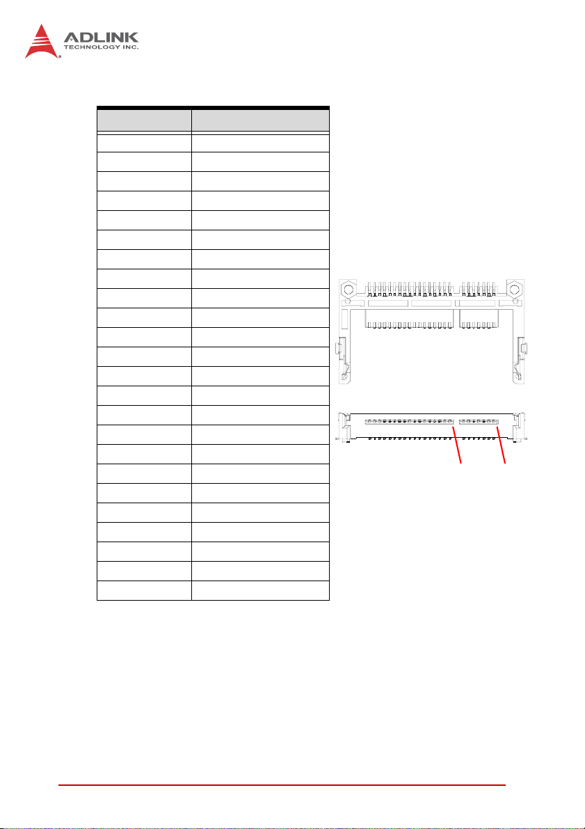
CompactPCI J1 Connector
Pin Z A B C D E F
25 GND +5V REQ64# ENUM# +3.3V +5V GND
24 GND CPCI_AD1 +5V CPCI_VIO CPCI_AD0 ACK64# GND
23 GND P3V3 CPCI_AD4 CPCI_AD3 P5V CPCI_AD2 GND
22 GND CPCI_AD7 GND P3V3 CPCI_AD6 CPCI_AD5 GND
21 GND P3V3 CPCI_AD9 CPCI_AD8 CPCI_M66EN CPCI_CBE-L0 GND
20 GND CPCI_AD12 GND VIO CPCI_AD11 CPCI_AD10 GND
19 GND P3V3 CPCI_AD15 CPCI_AD14 GND CPCI_AD13 GND
18 GND CPCI_SERR-L GND P3V3 CPCI_PAR CPCI_CBE-L1 GND
17 GND P3V3 NC NC GND CPCI_PERR-L GND
16 GND CPCI_DEVSEL-L CPCI_PCIXCAP VIO CPCI_STOP-L CPCI_LOCK-L GND
15 GND P3V3 CPCI_FRAME-L CPCI_IRDY-L NC CPCI_TRDY-L GND
12-14 Key
11 GND CPCI_AD18 CPCI_AD17 CPCI_AD16 GND CPCI_CBE-L2 GND
10 GND CPCI_AD21 GND P3V3 CPCI_AD20 CPCI_AD19 GND
9 GND CPCI_CBE-L3 NC CPCI_AD23 GND CPCI_AD22 GND
8 GND CPCI_AD26 GND VIO CPCI_AD25 CPCI_AD24 GND
7 GND CPCI_AD30 CPCI_AD29 CPCI_AD28 GND CPCI_AD27 GND
6 GND CPCI_REQ-L0 GND P3V3 CPCI_CLK0 CPCI_AD31 GND
5 GND NC NC CPCI_RESET-L GND CPCI_GNT-L0 GND
4 GND NC CPCI_HEALTHY -L VIO NC NC GND
3 GND CPCI_IRQA-L CPCI_IRQB-L CPCI_IRQC-L P5V CPCI_IRQD-L GND
2 GND cPCI_TCK-L P5V cPCI_TMS-L NC cPCI_TDI-L GND
1 GND P5V NC cPCI_TRST-L P12V P5V GND
Table 4-29: CompactPCI J1 Connector Pin Definition
62 Board Interfaces
Page 77

cPCI-3510
CompactPCI J2 Connector
Pin Z A B C D E F
22 GND GA4 GA3 GA2 GA1 GA0 GND
21 GND
20 GND
19 GND
18 GND
17 GND
16 GND
15 GND
14 GND
13 GND
12 GND
11 GND
10 GND
9GND
8GND
7GND
6GND
5GND
4GND
3GND
2GND
1 GND CLK1 GND REQ1# GNT1# REQ2# GND
PCI_CLK6 GND LAN2_TXDP1 LAN1_TXDP3 LAN1_TXDP1
PCI_CLK5 GND LAN2_TXDN1 LAN1_TXDN3 LAN1_TXDN1
GND GND LAN2_TXDP0 LAN1_TXDP2 LAN1_TXDP0
LAN2_TXDP3 LAN2_TXDP2 LAN2_TXDN0 LAN1_TXDN2 LAN1_TXDN0
LAN2_TXDN3 LAN2_TXDN2 J2_RSTJ CPCI_REQ_L6 CPCI_GNT_L6
CLK_PCIE8_N CLK_PCIE6_P DEGJ GND +5V
CLK_PCIE8_P CLK_PCIE6_N FALJ CPCI_REQ_L5 CPCI_GNT_L5
CLK_PCIE7_N CLK_PCIE5_P PCIE_RST-L
CLK_PCIE7_P CLK_PCIE5_N PCIE_RST-L VGA_HSY
PCIE8_RX_P PCIE_RST-L PCIE_RST-L VGA_VSY SATA_RX-P2
PCIE8_RX_N PCIE_TXP8 COM4_TX SATA_TX-P2 SATA_RX-N2
PCIE7_RX_P PCIE_TXN8 COM4_RX SATA_TX-N2 SATA_RX-P3
PCIE7_RX_N PCIE_TXP7 USB_0P SATA_TX-P3 SATA_RX-N3
PCIE6_RX_P PCIE_TXN7 USB_0N SATA_TX-N3 SATA_RX-P4
PCIE6_RX_N PCIE_TXP6 USB_3P SATA_TX-P4 SATA_RX-N4
PCIE5_RX_P PCIE5_RX_P USB_3N SATA_TX-N4 RGB_RED
PCIE5_RX_N PCIE_TXP5 USB_10P RS232_COM5_SEL-L RGB_GREEN
VIO PCIE_TXN5 USB_10N USB_OC0 RGB_BLUE
CLK4 GND GNT3# REQ4# GNT4#
CLK2 CLK3 SYSEN# GNT2# REQ3#
DDC_DAT
+5V
DDC_CLK
Ta ble 4-30: CompactPCI J2 Connecto r Pin De fini tion
Ethernet port
VGA
Serial A TA
PCI-Express
Serial port
USB port
GND
GND
GND
GND
GND
GND
GND
GND
GND
GND
GND
GND
GND
GND
GND
GND
GND
GND
GND
GND
Board Interfaces 63
Page 78

cPCI-R3P00 rJ2 Connector
Pin Z A B C D E F
22 GND NC NC NC NC NC GND
21 GND NC GND 2_ETH_B+ 1_ETH_D+ 1_ETH_B+ GND
20 GND NC GND 2_ETH_B- 1_ETH_D- 1_ETH_B- GND
19 GND GND GND 2_ETH_A+ 1_ETH_C+ 1_ETH_A+ GND
18 GND 2_ETH_D+ 2_ETH_C+ 2_ETH_A- 1_ETH_C- 1_ETH_A- GND
17 GND 2_ETH_D- 2_ETH_C- NC NC NC GND
16 GND NC NC NC GND +5V GND
15 GND NC NC NC NC NC GND
14 GND NC NC NC DDC_DAT +5V GND
13 GND NC NC NC VGA_HSY DDC_CLK GND
12 GND NC NC NC VGA_VSY 2_SATA_RX+ GND
11 GND NC NC COM4_TX 2_SATA_TX+ 2_SATA_RX- GND
10 GND NC NC COM4_RX 2_SATA_TX- 3_SATA_RX+ GND
9 GND NC NC 0_USB+ 3_SATA_TX+ 3_SATA_RX- GND
8 GND NC NC 0_USB- 3_SATA_TX- 4_SATA_RX+ GND
7 GND NC NC 1_USB+ 4_SATA_TX+ 4_SATA_RX- GND
6 GND NC NC 1_USB- 4_SATA_TX- RGB_RED GND
5 GND NC NC 10_USB+
4 GND NC NC 10_USB- USB1_10_OC RGB_BLUE GND
3 GND NC GND NC NC NC GND
2 GND NC NC NC NC NC GND
1 GND NC GND NC NC NC GND
Table 4-31: cPCI-R3P00 rJ2 Connector Pin Definition
RS232_COM5_SEL-L
Ethernet port
VGA
Serial A TA
PCI-Express
Serial port
USB port
RGB_GREEN GND
64 Board Interfaces
Page 79
cPCI-3510
cPCI-R3P00T rJ2 Connector
Pin Z A B C D E F
22 GND NC NC NC NC NC GND
21 GND NC GND NC NC NC GND
20 GND NC GND NC NC NC GND
19 GND GND GND NC NC NC GND
18 GND NC NC NC NC NC GND
17 GND NC NC NC NC NC GND
16 GND 4PE_CLK- 2_PE_CLK+ NC GND +5V GND
15 GND 4PE_CLK+ 2_PE_CLK- NC NC NC GND
14 GND 3PE_CLK+ 1_PE_CLK+ 4_PE_CLKE# DDC_DAT +5V GND
13 GND 3PE_CLK- 1_PE_CLK- 3_PE_CLKE# VGA_HSY DDC_CLK GND
12 GND 4PE_RX00+ 1_PE_CLKE# 2_PE_CLKE# VGA_VSY 2_SATA_RX+ GND
11 GND 4PE_RX00- 4PE_TX00+ COM4_TX 2_SATA_TX+ 2_SATA_RX- GND
10 GND 3PE_RX00+ 4PE_TX00- COM4_RX 2_SATA_TX- 3_SATA_RX+ GND
9GND 3PE_RX00- 3PE_TX00+ 0_USB+ 3_SATA_TX+ 3_SATA_RX- GND
8GND 2PE_RX00+ 3PE_TX00- 0_USB- 3_SATA_TX- 4_SAT A_RX+ GND
7GND 2PE_RX00- 2PE_TX00+ 1_USB+ 4_SATA_TX+ 4_SATA_RX- GND
6GND 1PE_RX00+ 2PE_TX00- 1_USB- 4_SATA_TX- RGB_RED GND
5GND 1PE_RX00- 1PE_TX00+ 10_USB+
4 GND NC 1PE_TX00- 10_USB- USB1_10_OC RGB_BLUE GND
3 GND NC GND NC NC NC GND
2 GND NC NC NC NC NC GND
1 GND NC GND NC NC NC GND
Table 4-32: cPCI-R3P00T rJ2 Connector Pin Definition
RS232_COM5_SEL-L
RGB_GREEN GND
VGA
Serial ATA
PCI-Express
Serial port
USB port
Board Interfaces 65
Page 80
4.12 Jumper Settings
Load BIOS Default Jumper (JP1)
The cPCI-3510 Load BIOS Default Jumper is located on the
DB-3CF/CFast daughter board. To load the default BIOS settings,
short pins 2-3 on JP1, then reinstall the jumper cap to pins 1-2.
BIOS Setting Connection JP1
Normal 1 – 2
Load default BIOS 2 – 3
Table 4-33: Load BIOS Default Jumper Settings
XMC VPWR Select Jumper on DB-3UMC (JPX1)
This jumper is located on the DB-3UMC board near JN1/2 and
selects the XMC VPWR setting. 5V is set by default.
Mode Connection JPX1
+5V (Default) 1 – 2
+12V 2 – 3
Table 4-34: XMC VPWR Select Jumper Settings
PMC V(I/O) Select Jumper on DB-3UMC (JPX2)
This jumper is located on the DB-3UMC board near JN1/2 and
selects the PMC V(I/O) setting. 3.3V is set by default.
Mode Connection JPX2
+5V 1 – 2
+3.3V (Default) 2 – 3
Table 4-35: PMC V(I/O) Select Jumper Settings
66 Board Interfaces
Page 81

5 Getting Started
This chapter describes the following installation procedur es fo r the
cPCI-3510 and rear transition module:
X CPU and Heatsink
X 2.5" SATA storage drive
X CFast card
X PCI Mezzanine Card
X Processor blade installation to chassis
X RTM installation to chassis
5.1 CPU and Heatsink
The cPCI-3510 Series come with CPU and heatsink pre-installed.
Removal of heatsink/CPU by users is not recommended. Please
contact your ADLINK service representative for assistance.
cPCI-3510
Getting Started 67
Page 82
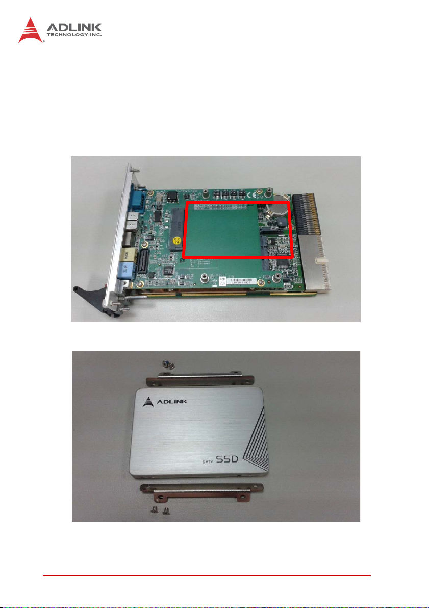
5.2 SATA Drive Installation
The cPCI-3510D/P/L/M 2/3-slot versions provide space to install a
slim type 2.5" Serial-ATA storage drive.
Installing a SATA Drive - cPCI-3510D/G/P/L/M
1. A 2.5" SATA drive can be assembled in the location
marked as below.
2. 2.Prepare a 2.5" SATA drive and locate the brackets and
screws in the accessory kit.
68 Getting Started
Page 83
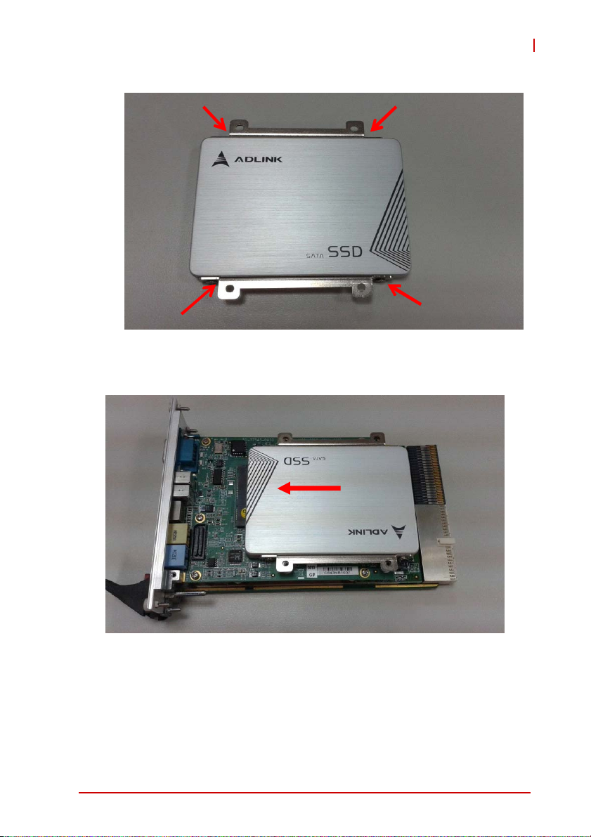
cPCI-3510
3. Screw the brackets to the 2.5" SATA drive.
4. Align the drive assembly with the cPCI-3510 and insert it
into the onboard SATA connector until it is properly
seated.
Getting Started 69
Page 84
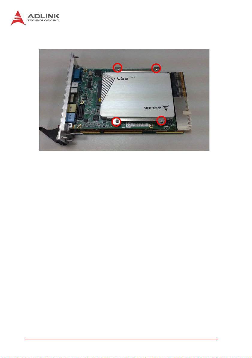
5. Secure the hard drive assembly to the cPCI-3510 with
four M2.5 screws provided.
70 Getting Started
Page 85
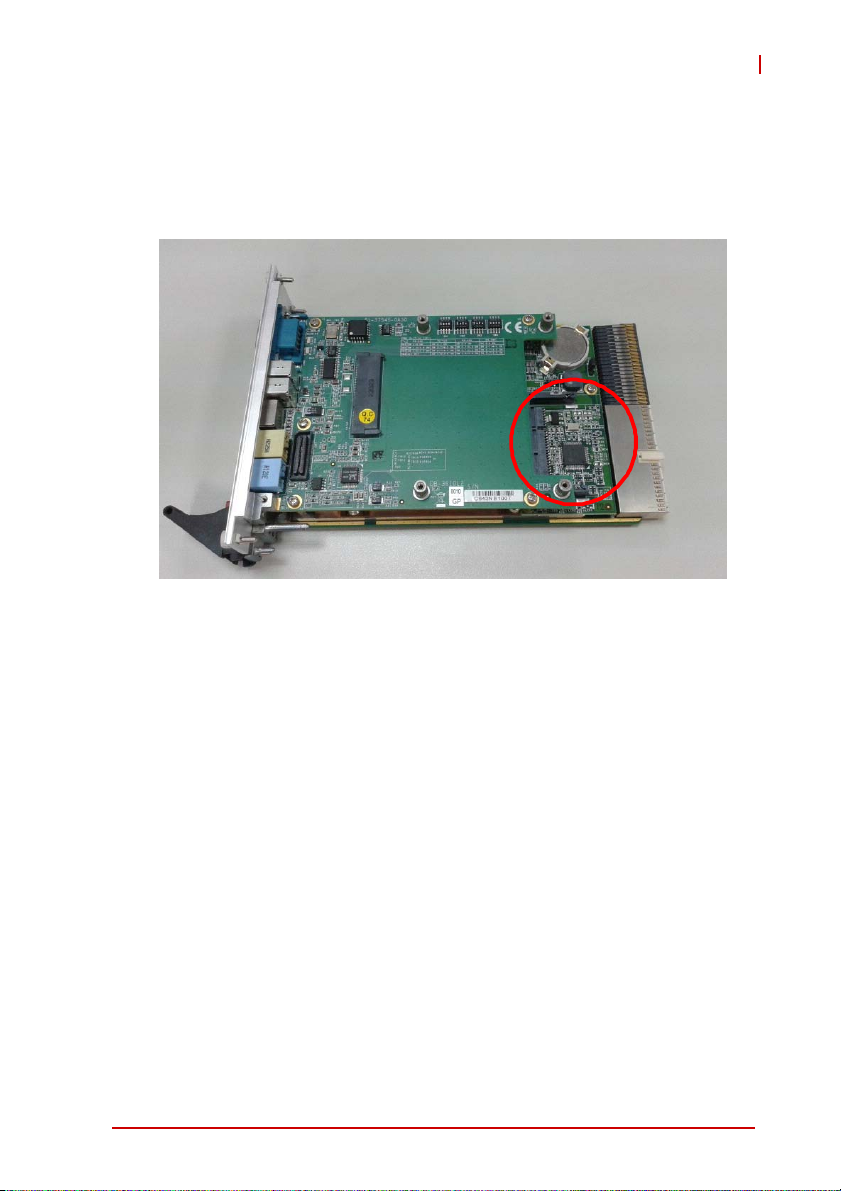
cPCI-3510
5.3 Installing a CFast Card
To install a CFast card, locate the CFast connector on the
DB-3CFAST daughter board and insert the card until it is properlly
seated.
Getting Started 71
Page 86

5.4 Installing the cPCI-3510 to the Chassis
The cPCI-3510 may be installed in a system or peripheral slot of a
3U CompactPCI chassis. These instructions are for reference
only. Refer to the user guide that comes with the chassis for more
information.
1. Be sure to select the correct slot depending on the operational purpose of the module. The system power may
now be powered on or off.
2. Remove the blank face cover from the selected slot, if
necessary.
3. Press down on the release catches of the cPCI-3510
ejector handles.
4. Remove the black plastic caps securing the mounting
screws to the front panel.
5. Align the module’s top and bottom edges to the chassis
card guides, and then carefully slide the module into the
chassis. A slight resistance may be felt when inserting
the module. If the resistance it too strong, check if there
are bent pins on the backplane or if the board’s connector pins are not properly aligned with connectors on the
backplane. Then push the board until it is completely
flush with the chassis.
6. Push the ejector handles outwards to secure the module
in place, and then fasten the screws on the module front
panel.
7. Connect the cables and peripherals to the board, and
then turn the chassis on if necessary.
72 Getting Started
Page 87

cPCI-3510
5.5 RTM Installation - cPCI-R3P00(T)
The installation and removal procedures for a RTM are the same
as those for CompactPCI boards. Because they are shorter than
front boards, pay careful attention when inserting or removing
RTMs.
Refer to previous sections for peripheral connectivity of all
I/O ports on the RTM. When installing the cPCI-3510 Series and
related RTMs, make sure the RTM is the correct matching model.
You must install the correct RTM to enable functions (I/O interfaces) on the rear panel. Installation of non-compatible RTMs
NOTE:
NOTE:
may damage the system board and/or other RTMs.
Getting Started 73
Page 88

This page intentionally left blank.
74 Getting Started
Page 89

6 Driver Installation
The cPCI-3510 drivers are available from the ADLINK All-In-One
DVD at X:\cPCI\cPCI-3510\, or from the ADLINK website
(http://www.adlinktech.com/PD/web/PD_detail.php?cKind=&
pid=1291). ADLINK provides validated drivers for Windows 7
64-bit. We recommend using these drivers to ensure compatibility.
The VxWorks BSP can be downloaded from the cPCI-3510 product page on the ADLINK website
6.1 cPCI-3510 Drivers
The following describes the cPCI-3510 driver installation procedures for Windows 7 64-bit. Install the Windows operating system
before installing any driver. Most standard I/O device drivers are
installed during Windows installation.
1. Before beginning Windows inst allation, save the AHCI driver to
a USB flash drive. During Windows installation, install the
AHCI driver from the USB flash drive when prompted.
2. Install the chipset driver by extracting and running the pro-
gram in ...\Chipset\Intel Chipset Device Software_
All OS_9.4.0.1017.zip.
cPCI-3510
3. Install the graphics driver and utilities by extracting and run-
ning the program in ...\Graphics\Intel® HD Graphics 4600_
Win7_64bit_9.18.10.3220.zip.
4. Install the Ethernet Controller driver by following the steps
described in "6.2 Ethernet Controller Driver” on page 76.
5. Install the
extracting and running the program in
Management Engine Interface 9.0.0.1209.zip
6. Install the TPM driver by extracting and running the program in
…\TPM\Infineon_Trusted_Platform_Module_2.1.1.0.zip.
7. Install the audio driver and utilities by extracting and running
the program in …\Audio\Realtek_High Definition Audio_
Win7_8_64_6.0.1.6873.zip.
Driver Installation 75
Management Engine (ME) driver
...\Chipset\Intel
and utilities by
.
Page 90
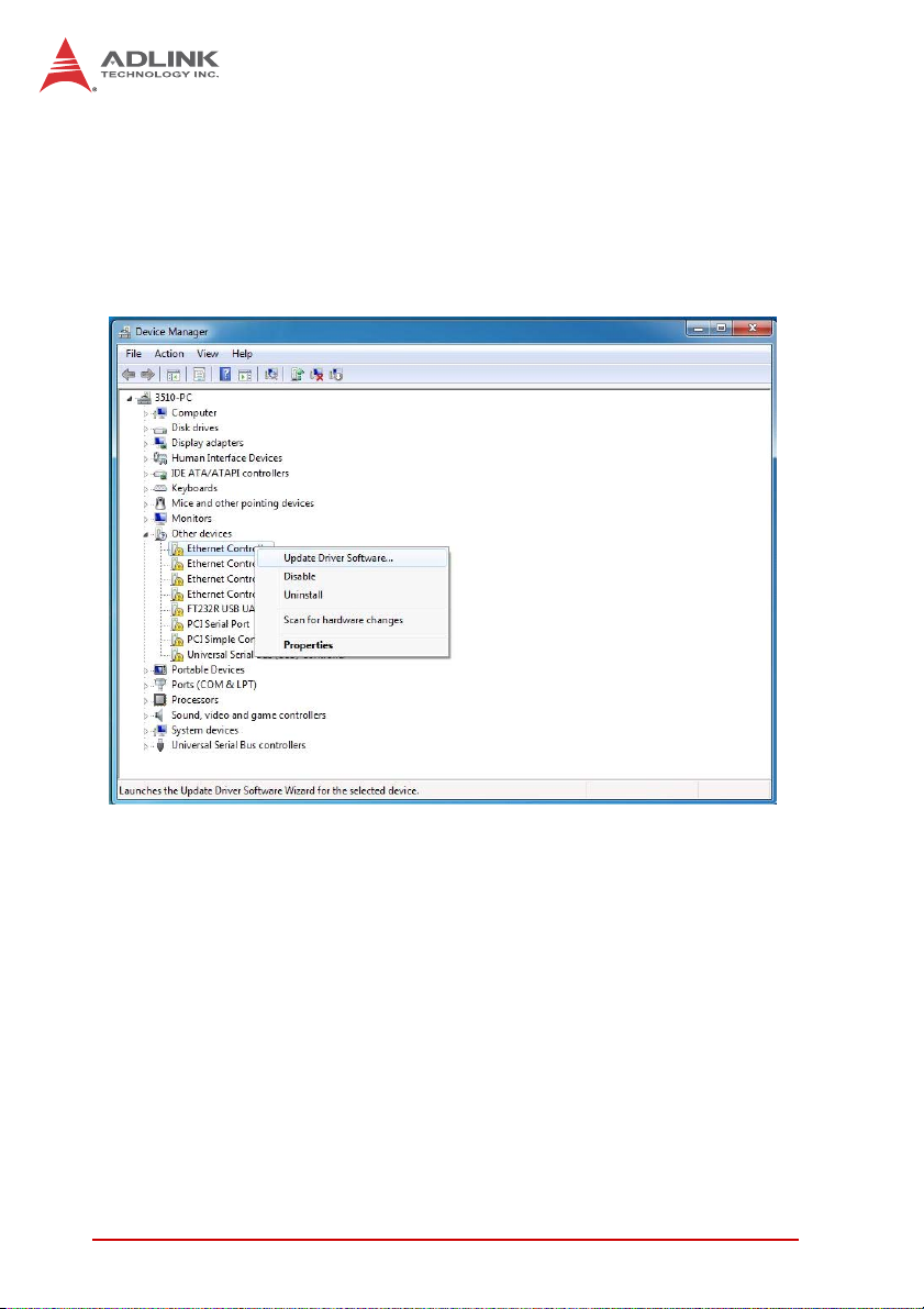
6.2 Ethernet Controller Driver
1. Extract the contents of …\LAN\Intel® I210 Gigabit Network connection_Win7 64bit_12.7.28.0.zip.
2. Open the Device Manager and go to Other Devices. You will
see a "question mark" next to Ethernet Controller R-click on
Ethernet Controller and choose "Update Driver Software…".
76 Driver Installation
Page 91

cPCI-3510
3. Click “Browse my computer for driver software”.
4. Navigate to the folder where you extracted the contents of the
zip file and click “OK”. Click “Next” to install the driver.
Driver Installation 77
Page 92
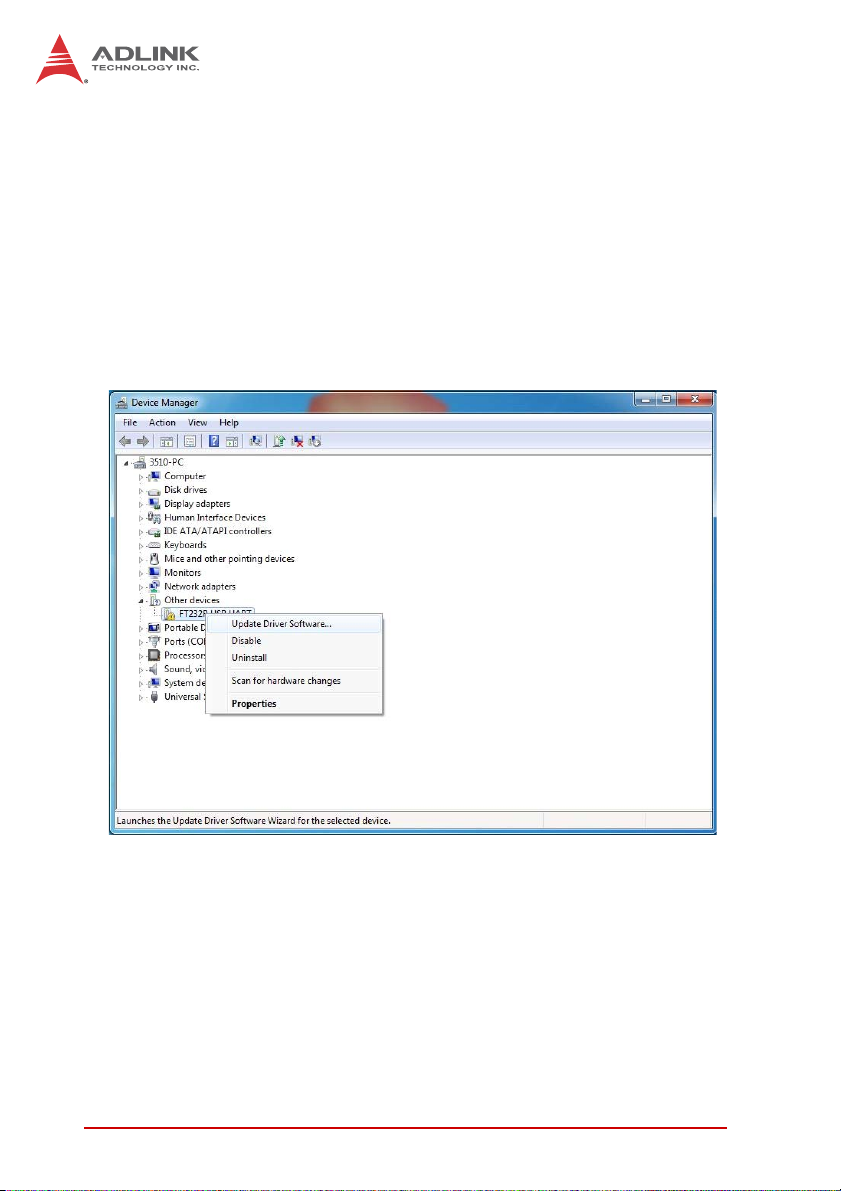
6.3 USB-to-Serial Converter Driver (RTM)
The COM5 serial port on the cPCI-R3P00(T) is converted from the
USB3 port by a USB-to-serial converter (see " cPCI-R3P00 RTM”
on page 17). To install the driver for the converter, follow the procedure below.
1. Extract the contents of …\cPCI-3510\COM\CDM 2.08.28
WHQL Certified-x64.zip.
2. Open the Device Manager and go to Other Devices. You will
see a "question mark" next to FT2332R USB UART. R-click on
FT2332R USB UART and choose "Update Driver Software…".
78 Driver Installation
Page 93
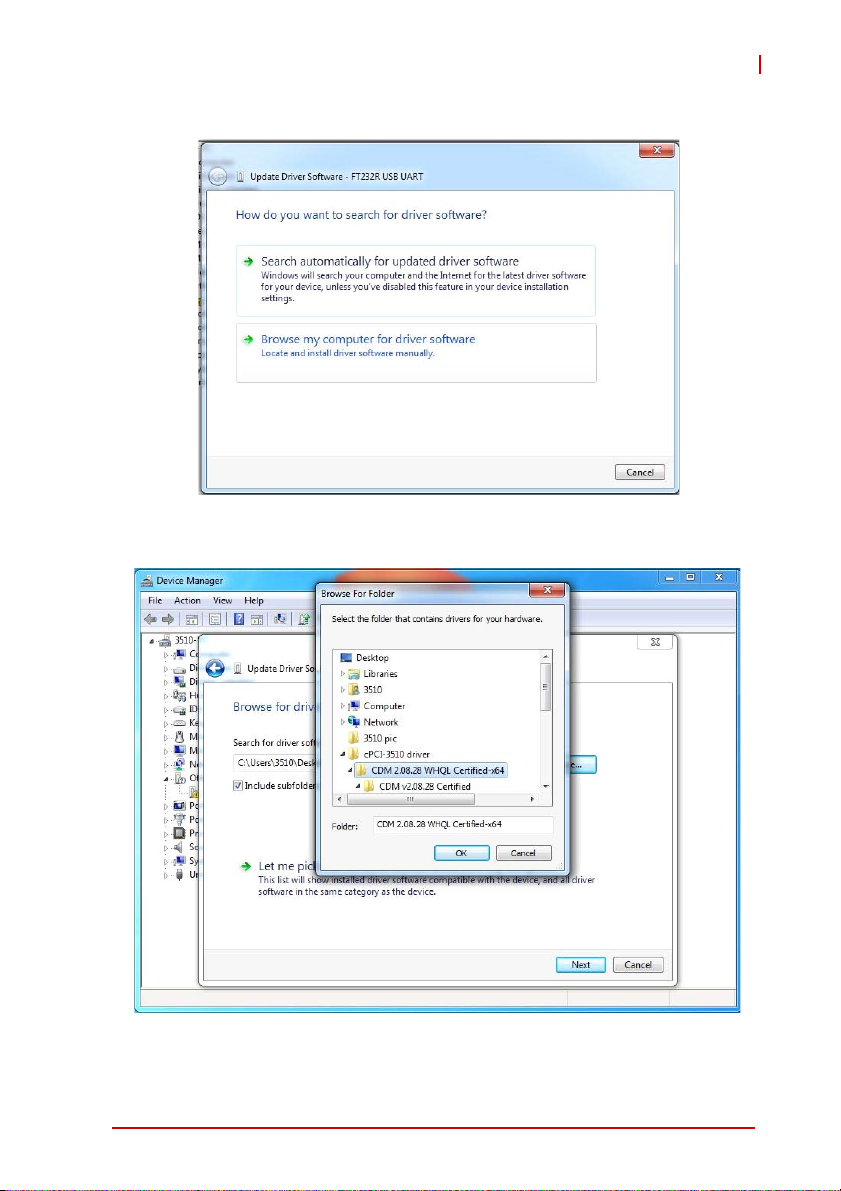
cPCI-3510
3. Click “Browse my computer for driver software”.
4. Navigate to the folder where you extracted the contents of the
zip file and click “OK”. Click “Next” to install the driver
Driver Installation 79
Page 94

This page intentionally left blank.
80 Driver Installation
Page 95

7 Watchdog Timer
This section describes the operation of the cPCI-3510’s watchdog
timer (WDT). The primary function of the WDT is to monitor the
cPCI-3510's operation and to reset the system if a software application fails to function as prog rammed. The following WDT functions may be controlled using a software application:
X enabling and disabling
X set and get current configuration
X reloading timeout value
The cPCI-3510 custom WDT functionality is implemented using an
Intelligent Platform Management Controller (IPMC) and controlled
using Intelligent Platform Management Interface (IPMI) commands.
7.1 Setting the Watchdog by IPMI Commands
The following section describes how to set the WDT functions
using IPMI commands. For more detailed information about IPMI
commands, please refer to IPMI specification: Intelligent Platform
Management Interface Specification Second Generation v2.0.
cPCI-3510
WDT Commands
These commands enable the watchdog function, set the countdown period, and reload the timeout value periodically to keep it
from resetting the system. If the timer countdown value is not
reloaded, the watchdog resets the system hardware after the
counter reaches zero.
Command NetFn Code Cmd Code
Reset Watchdog Timer App (18h) 22h
Set Watchdog Timer App (18h) 24h
Get Watchdog Timer App (18h) 25h
Watchdog Timer 81
Page 96
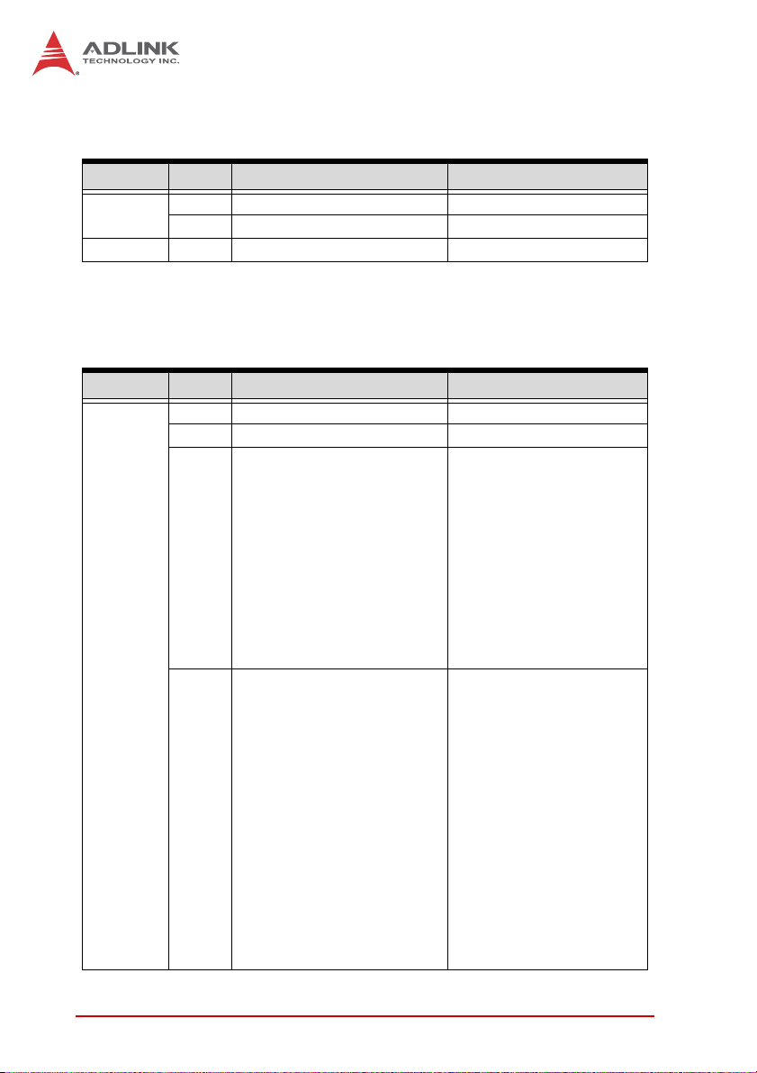
Reset Watchdog Timer
This command is used to reload the WDT.
Action Byte Value Description
Request
Response 0 Complete Code 00h means OK
0 18h NetFn/LUN
1 22h Defined command
Set Watchdog Timer
This command is used to start and restart the Watchdog Timer
using the specified countdown value.
Action Byte Value Description
0 18h NetFn/LUN
1 24h Defined command
[7] - 1b = don’t log
[6] - 1b = don’t stop timer*
[5:3] - reserved
[2:0] - timer use
000b = reserved
2
Request
001b = BIOS FRB2
010b = BIOS/POST
011b = OS Load
100b = SMS/OS
101b = OEM
110b -111b = reserved
[7] - reserved
[6:4] - pre-timeout interrupt
000b = none
001b = SMI (optional)
010b = NMI / Diagnostic
Interrupt (optional)
011b = Messaging Interrupt
3
100b,111b = reserved
[3] - reserved
[2:0] - timeout action
000b = no action
001b = Hard Reset
010b = Power Down
01 1b = Power Cycle
100b,111b = reserved
Timer Use
Timer Actions
82 Watchdog Timer
Page 97
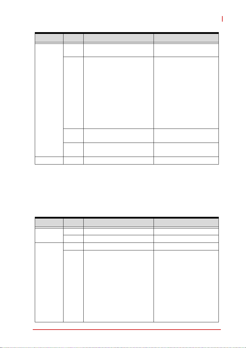
cPCI-3510
Action Byte Value Description
Request
Response 0 Complete Code 00h means OK
*Note: don’t stop timer: If the WDT is already running, the countdown
value will get set to the specified value and countdown will continue from
that point. If timer is already stopped, it will remain stopped. If the pretimeout interrupt bit is set, it will get cleared.
4 1h~ffh ( ‘1h’ based.)
[7] - reserved
[6] - reserved
[5] - OEM
[4] - SMS/OS
[3] - OS Load
5
[2] - BIOS/POST
[1] - BIOS FRB2
[0] - reserved
0b = leave alone
1b = clear timer use
expiration bit
00h~ffh ,LS byte (100 ms/
6
count)
00h~ffh ,MS byte (100 ms/
7
count)
Pre-timeout interval in
seconds.
Timer Use Expiration flags
clear
Initial countdown value
Initial countdown value
Get Watchdog Timer
This command is used to get the current WDT configuration.
Action Byte Value Description
Request
Response
Watchdog Timer 83
0 18h NetFn/LUN
1 25h Defined command
0 Complete Code 00h means OK
[7] - 1b = don’t log
[6] - 1b = don’t stop timer
[5:3] - reserved
[2:0] - timer use
000b = reserved
1
001b = BIOS FRB2
010b = BIOS/POST
011b = OS Load
100b = SMS/OS
101b = OEM
110b -111b = reserved
Timer Use
Page 98
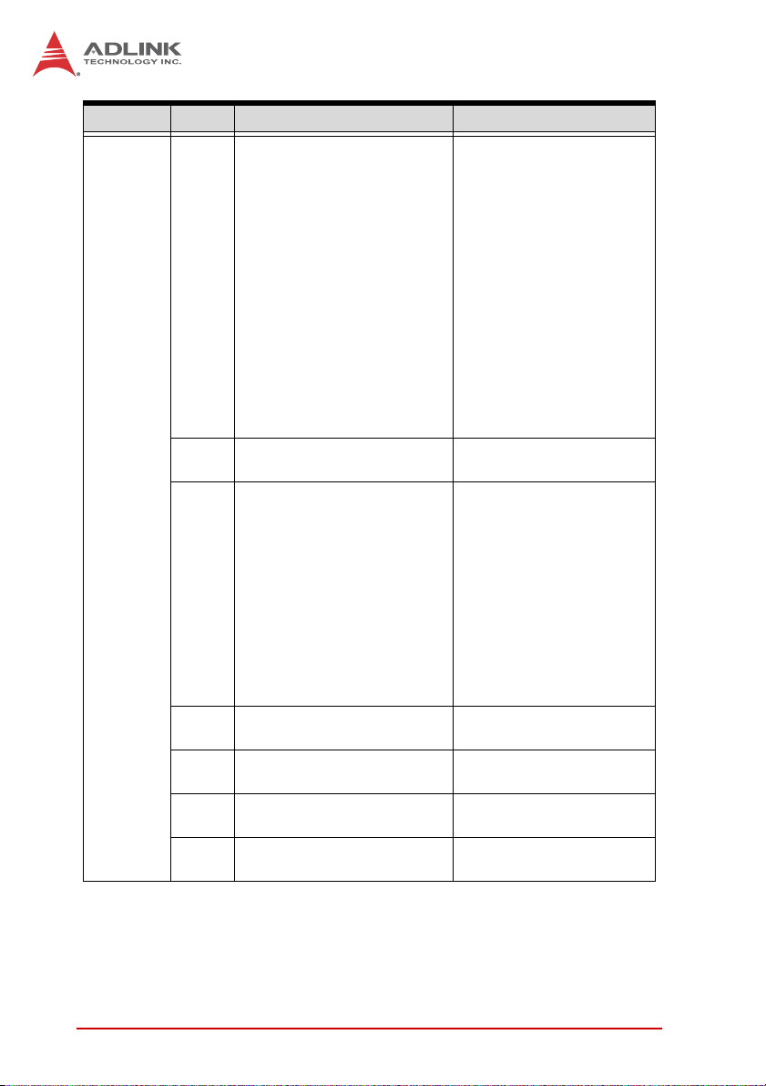
Action Byte Value Description
[7] - reserved
[6:4] - pre-timeout interrupt
000b = none
001b = SMI (optional)
010b = NMI / Diagnostic
Interrupt (optional)
011b = Messaging Interrupt
2
Response
100b,111b = reserved
[3] - reserved
[2:0] - timeout action
000b = no action
001b = Hard Reset
010b = Power Down
01 1b = Power Cycle
100b,111b = reserved
1h~ffh ( ‘1h’ based.) Pre-timeout interval in
3
[7] - reserved
[6] - reserved
[5] - OEM
[4] - SMS/OS
[3] - OS Load
4
[2] - BIOS/POST
[1] - BIOS FRB2
[0] - reserved
0b = leave alone
1b = clear timer use
expiration bit
00h~ffh ,LS byte (100 ms/
5
count)
00h~ffh ,MS byte (100 ms/
6
count)
00h~ffh ,LS byte (100 ms/
7
count)
00h~ffh ,MS byte (100 ms/
8
count)
Timer Actions
seconds.
Timer Use Expiration flags
clear
Initial countdown value
Initial countdown value
Present countdown value
Present countdown value
84 Watchdog Timer
Page 99

cPCI-3510
Example WDT Programming Procedure
Configuration of the watchdog timer is via serial interface. A
detailed description of the WDT IPMI commands can be found
above. The following example shows the procedure for configuring
the WDT works over a serial console. See “Communications with
IPMC” on page 129. for more information.
[18 00 24 43 01 01 08 50 00] => Step 1: Set parameters to WDT
[1C 00 24 00] => Step 1: Response of setting OK.
[18 00 22] => Step 2: Tri gger WDT
[1C 00 22 00] => Step 2: Response of trigger OK.
[18 00 25] => Get curre nt configuration
[1C 00 25 00 43 01 01 00 50 00 28 00] => Res ponse during WDT countdow n
<A>: BMC Watchdog expired
<A>: Re s e t al e r t
[18 00 25] => Get curre nt configuration
[1C 00 25 00 03 01 01 08 50 00 00 00
] => Response after Reset
Figure 7-1: Example procedure for configuring the WDT over serial console
1. Configure the WDT by using the raw IPMI command
"Set Watchdog Timer" described above.
"Set Watchdog Timer" Command:
[18 00 24 43 01 01 08 50 00]
Description:
0x18: Net function. Defined in IPMI specification
0x00: Bus ID. Usually "0x00".
0x24: Command. Defined in IPMI specification.
0x43: Set "Don’t stop timer" and "OS Load".
0x01: Hard Reset.
0x01: Pre-timeout interval in seconds.
0x08: Timer Use Expiration flags cleared by OS Load.
0x50: Initial countdown value. Sets the interval
before watchdog timer expires.
80 count: 100ms * 80 = 8000 ms = 8 seconds
Successful response to command:
[1C 00 24 00]
Watchdog Timer 85
Page 100

2. Reload the WDT counter by using the raw IPMI command
"Reset Watchdog Timer".
"Reset Watchdog Timer" Command:
[18 00 22]
Successful response to Command:
[1C 00 22 00]
3. Get the WDT configuration by using the "Get Watchdog
Timer" command.
"Get Watchdog Timer" Command:
[18 00 25]
Successful response to Command:
[1C 00 25 00 43 01 01 00 50 00 28 00]
0x18: Net function. Defined in IPMI specification
0x00: Bus ID. Usually "0x00".
0x25: Command. Defined in IPMI specification.
0x43: Get timer operation status and "OS Load".
The first nibble is "4". This means the timer is
running. If the first nibble is "0", then the
watchdog timer has timed out and stopped. The
second nibble is "Timer Use". A value of "3"
means the option is set to "OS Load".
0x01: Hard Reset.
0x01: Pre-timeout interval in seconds.
0x00: Timer Use Expiration flags clear.
0x50: Initial countdown value. The current interval
before the watchdog timer expires.
80 count. 100ms * 80 = 8000ms = 8 seconds.
0x10: Present countdown value. How much time is left
before timer expires.
16 count: 100ms * 16 = 1600ms = 1.6 seconds
86 Watchdog Timer
 Loading...