

Page 1

CoreModule® 720
Single Board Computer
Reference Manual
P/N 50-1Z105-1020
Page 2

Notice Page
DISCLAIMER
ADLINK Technology, Incorporated makes no representations or warranties with respect to the contents of
this manual or of the associated ADLINK products, and specifically disclaims any implied warranties of
merchantability or fitness for any particular purpose. ADLINK shall under no circumstances be liable for
incidental or consequential damages or related expenses resulting from the use of this product, even if it has
been notified of the possibility of such damages. ADLINK reserves the right to revise this publication from
time to time without obligation to notify any person of such revisions. If errors are found, please contact
ADLINK at the address shown at the bottom of this page.
TRADEMARKS
CoreModule and the Ampro logo are registered trademarks, and ADLINK, Little Board, LittleBoard,
MightyBoard, MightySystem, MilSystem, MiniModule, ReadyBoard, ReadyBox, ReadyPanel,
ReadySystem, and RuffSystem are trademarks of ADLINK Technology, Inc. All other marks are the
property of their respective companies.
REVISION HISTORY
Revision Reason for Change Date
1000 Initial Release Jan/12
1010 Added Appendix B to describe video adapter board; added
temperature monitor description to Chapter 3; updated
manufacturers and models of components in Table 2-1.; added
manufacturers and models of headers in Table 2-2.
1020 Revised COM interrupt channel assignments in Ta bl e 3 -1; removed
COM addresses from Tab le 3- 3; updated contact addresses in
Appendix A
Feb/13
Sept/13
ADLINK Technology, Incorporated
5215 Hellyer Avenue, #110
San Jose, CA 95138-1007
Tel. 408 360-0200
Fax 408 360-0222
www.adlinktech.com
© Copyright 2012, 2013 ADLINK Technology, Incorporated
Audience
This manual provides reference only for computer design engineers, including but not limited to hardware
and software designers and applications engineers. ADLINK Technology, Inc. assumes you are qualified to
design and implement prototype computer equipment.
ii Reference Manual CoreModule 720
Page 3

Contents
Chapter 1 About This Manual ....................................................................................................1
Purpose of this Manual ....................................................................................................................1
References ......................................................................................................................................1
Chapter 2 Product Overview......................................................................................................3
PC/104 Architecture ........................................................................................................................3
Product Description..........................................................................................................................4
Module Features ........................................................................................................................5
Block Diagram ...........................................................................................................................7
Major Component (ICs) Definitions .................................................................................................8
Header, Connector, and Socket Definitions...................................................................................11
Jumper Header Definitions ...........................................................................................................13
Specifications.................................................................................................................................14
Physical Specifications .............................................................................................................14
Mechanical Specifications ........................................................................................................15
Power Specifications ................................................................................................................16
Environmental Specifications .................................................................................................17
Thermal/Cooling Requirements ................................................................................................18
Chapter 3 Hardware .................................................................................................................19
Overview ........................................................................................................................................19
CPU ...............................................................................................................................................20
Graphics.........................................................................................................................................20
Memory ........................................................................................................................................20
Interrupt Channel Assignments .....................................................................................................21
Memory Map .................................................................................................................................21
I/O Address Map ...........................................................................................................................22
Serial Interfaces ............................................................................................................................23
USB Interfaces ..............................................................................................................................24
Ethernet Interface .........................................................................................................................26
Video (SDVO/LVDS) Interfaces ....................................................................................................27
Power Interface .............................................................................................................................29
User GPIO Interface .....................................................................................................................29
Utility Interface ..............................................................................................................................30
Power Button ...........................................................................................................................30
Reset Switch ............................................................................................................................30
Speaker ....................................................................................................................................30
System Management Bus (SMBus) ..............................................................................................31
CAN Bus Interface ........................................................................................................................31
I2C Interface .................................................................................................................................32
System Fan....................................................................................................................................32
Battery............................................................................................................................................33
Ethernet External LED ..................................................................................................................33
Miscellaneous ...............................................................................................................................33
SSD (Solid State Drive) ............................................................................................................33
Real Time Clock (RTC) ..........................................................................................................33
Oops! Jumper (BIOS Recovery) ...............................................................................................34
CoreModule 720 Reference Manual iii
Page 4

Contents
Serial Console ........................................................................................................................ 34
Serial Console Setup ......................................................................................................... 34
Hot (Serial) Cable .............................................................................................................. 34
Temperature Monitoring .......................................................................................................... 34
Watchdog Timer ...................................................................................................................... 35
Chapter 4 BIOS Setup .............................................................................................................. 37
Introduction.................................................................................................................................... 37
Entering BIOS Setup (Local Video Display) ............................................................................. 37
Entering BIOS Setup (Serial Port Console) ............................................................................ 37
OEM Logo Utility ...................................................................................................................... 38
Logo Image Requirements....................................................................................................... 38
BIOS Setup Menus ....................................................................................................................... 39
Main BIOS Setup Screen ...................................................................................................... 39
Advanced BIOS Setup Screen .............................................................................................. 40
Chipset BIOS Setup Screen .................................................................................................. 43
Boot BIOS Setup Screen ...................................................................................................... 45
Security BIOS Setup Screen ............................................................................................... 46
Save & Exit BIOS Setup Screen ........................................................................................... 47
Appendix A Technical Support ................................................................................................. 49
Appendix B Video Adapter Board ............................................................................................. 53
Overview ....................................................................................................................................... 53
Product Description ....................................................................................................................... 53
Video Adapter Board Header Signals .......................................................................................... 54
Index .................................................................................................................................................. 55
List of Figures
Figure 2-1. Stacking PC/104-Plus Modules with the CoreModule 720 ...................................... 4
Figure 2-2. Functional Block Diagram ....................................................................................... 7
Figure 2-3. Component Locations (Top Side).......................................................................... 10
Figure 2-4. Component Locations (Bottom Side) .................................................................... 10
Figure 2-5. Connector Pin Sequences .................................................................................... 12
Figure 2-6. Header, Connector, and Socket Locations (Top Side) .......................................... 13
Figure 2-7. Jumper Header Locations (Top Side) ................................................................... 14
Figure 2-8. Mechanical Overview (Top Side) .......................................................................... 15
Figure 2-9. E6XXT Peak In-Rush Current and Duration.......................................................... 16
Figure 2-10. Stack Heights of Cooling Assemblies .................................................................. 18
Figure 3-1. Oops! Jumper Serial Port (DB9)............................................................................ 34
Figure 3-2. Serial Console Jumper .......................................................................................... 34
Figure 4-1. Main BIOS Setup Screen ...................................................................................... 39
Figure 4-2. Advanced BIOS Setup Screen .............................................................................. 40
Figure 4-3. Chipset BIOS Setup Screen.................................................................................. 43
Figure 4-4. Boot BIOS Setup Screen....................................................................................... 45
Figure 4-5. Security BIOS Setup Screen ................................................................................. 46
Figure 4-6. Save & Exit BIOS Setup Screen ........................................................................... 47
iv Reference Manual CoreModule 720
Page 5

List of Tables
Table 2-1. Major Component Descriptions and Functions ........................................................8
Table 2-2. Module Header and Connector Descriptions .........................................................11
Table 2-3. Jumper Settings .....................................................................................................13
Table 2-4. Weight and Footprint Dimensions..........................................................................14
Table 2-5. Power Supply Requirements .................................................................................16
Table 2-6. Environmental Requirements.................................................................................17
Table 2-7. ADLINK Optional Cooling Solutions.......................................................................18
Table 3-1. Interrupt Channel Assignments..............................................................................21
Table 3-2. Memory Map ..........................................................................................................21
Table 3-3. I/O Address Map ....................................................................................................22
Table 3-4. Serial 1 (COM0) Interface Pin Signal Descriptions (J10) .......................................23
Table 3-5. Serial 2 (COM1, 2, and 3) Interface Pin Signal Descriptions (J11) ........................24
Table 3-6. USB0 and USB1 Interface Pin Signals (J12) .........................................................24
Table 3-7. USB2 and USB3 Interface Pin Signals (J14) .........................................................25
Table 3-8. USB4 and USB5 Interface Pin Signals (J13) .........................................................25
Table 3-9. Ethernet Interface Pin Signal Descriptions (J8) .....................................................26
Table 3-10. SDVO Interface Pin Signals (J15)..........................................................................27
Table 3-11. LVDS Video Interface Pin Signals (J23) ................................................................28
Table 3-12. Power Interface Pin Signals (J19)..........................................................................29
Table 3-13. User GPIO Interface Pin Signals (J3) ....................................................................29
Table 3-14. Utility Interface Pin Signals (J22) ...........................................................................30
Table 3-15. SMBus Reserved Addresses .................................................................................31
Table 3-16. SMBus Pin Signals (J24) .......................................................................................31
Table 3-17. CAN Interface Pin Signals (J4) .............................................................................31
Table 3-18. I2C Interface Pin Signals (J6) ...............................................................................32
Table 3-19. System Fan Pin Signals (J21) ...............................................................................32
Table 3-20. External Battery Input Header (J20) .....................................................................33
Table 3-21. Ethernet External LED Pin Signals (J9) .................................................................33
Table 4-1. BIOS Setup Menus ................................................................................................39
Table A-1. Technical Support Contact Information..................................................................49
Table B-1. VGA Interface Pin Signals (J2) ..............................................................................54
Contents
CoreModule 720 Reference Manual v
Page 6

Contents
vi Reference Manual CoreModule 720
Page 7

Chapter 1 About This Manual
Purpose of this Manual
This manual is for designers of systems based on the CoreModule® 720 Single Board Computer (SBC). This
manual contains information that permits designers to create an embedded system based on specific design
requirements.
Information provided in this reference manual includes:
• Product Overview
• Hardware Specifications
• BIOS Setup information
• Technical Support Contact Information
Information not provided in this reference manual includes:
• Detailed chip specifications (refer to the References section of this chapter)
• Internal component operation
• Internal registers or signal operations
• Bus or signal timing for industry-standard busses and signals
• Pin-signal definitions for industry-standard interfaces
References
The following list of references may help you successfully complete your custom design.
Expansion Bus Specifications
• PC/104 Specification, Revision 2.5, November, 2003
• PC/104-Plus Specification, Revision 2.0, November, 2003
Web site: http://www.pc104.org
• PCI Specification, Revision 3.0, August 12, 2002
Web site: http://www.pcisig.com
• LPC Bus Specification, Revision 1.1, August, 2002
Specification: http://www.intel.com/design/chipsets/industry/25128901.pdf
• PCIe Specification, Revision 1.0a, April 15, 2003
Specification (for members): http://www.pcisig.com/specifications/
2
• I
C Bus Specification Version 2.1
Specification: http://www.nxp.com/documents/other/39340011.pdf
• AMI BIOS Aptio TSE User’s Guide
Data sheet: http://www.ami.com/support/doc/AMI_TSE_User_Manual_PUB.pdf
• Bosch CAN specification version 2.0B
Specification: http://www.can-cia.org/fileadmin/cia/specifications/CAN20B.pdf
CoreModule 720 Reference Manual 1
Page 8

Chapter 1 About This Manual
Chip Specifications
The following integrated circuits (ICs) are used in the CoreModule 720 single board computer:
• Intel Corporation and the Atom™ E6XXT processors
Data sheet: http://download.intel.com/embedded/processor/datasheet/324208.pdf
• Micron Technology, Inc. and the MT47H256M8EB-25E DDR2 on-board System Memory
Web sit e : http://www.micron.com/parts/dram/ddr2-sdram/mt47h256m8eb-25e
• Intel Corporation and the PCH EG20T chip, used for the I/O Hub (Southbridge)
Data sheet: http://download.intel.com/embedded/chipsets/datasheet/324211.pdf
• Texas Instruments and the SN65HVD1040D CAN Transceiver
Web site: http://focus.ti.com/lit/ds/symlink/sn65hvd1040.pdf
• Intel Corporation and the 82574IT chip used for the Gigabit Ethernet controller
Data sheet: http://
download.intel.com/design/network/datashts/82574.pdf
• Atmel Corporation and the AT25128B-SSHL-B Ethernet EEPROM
Data sheet: http://www.atmel.com/dyn/resources/prod_documents/doc8535.pdf
• Fintek and the F85226FG, LPC-to-ISA Bridge
Data sheet:
http://pdf1.alldatasheet.com/datasheet-pdf/view/257962/FINTEK/F85226FG.html
• PLX Technology and the PEX8112 PCIe-to-PCI Bridge
Data sheet:
http://www.plxtech.com/products/expresslane/pex8112#technicaldocumentation
• Atmel Corporation and the AT25640B-SSHL SPI EEPROM
Data sheet: http://www.atmel.com/dyn/resources/prod_documents/doc8535.pdf
• Maxim Integrated Products and the MAX3245EEUI+ RS-232 Serial Port Transceiver
Web site: http://www.maxim-ic.com/datasheet/index.mvp/id/1847
• ON Semiconductor and the ADM1032ARMZ Temperature Monitor
Data sheet: http://www.onsemi.com/pub_link/Collateral/ADM1032-D.PDF
• Greenliant and the GLS85LS1008P Solid State NANdrive
Data sheet: http://www.greenliant.com/dotAsset/46411.pdf
NOTE If you are unable to locate the datasheets using the links provided, search the internet
using the name of the manufacturer or component model and locate the documents
you need.
2 Reference Manual CoreModule 720
Page 9

Chapter 2 Product Overview
This overview presents information about the PC/104 architecture and the CoreModule 720 Single Board
Computer (SBC). After reading this chapter you should understand:
• PC/104 architecture
• Product description
• Major components (ICs)
• Headers, Connectors, and Sockets
• Specifications
PC/104 Architecture
The PC/104 architecture affords a great deal of flexibility in system design. You can build a simple system
using only a CoreModule 720 SBC, input/output devices connected to the serial, USB, or SATA ports, and
the on-board Solid State Disk storage device. To expand a simple CoreModule system, simply add selfstacking PC/104 and PC/104-Plus expansion boards to provide additional capabilities, such as:
• Additional serial and parallel ports
• Analog or high-speed digital I/O
Data Acquisition (Analog In/Out)
USB 2.0 expansion modules
IEEE 1394 (FireWire) expansion modules
Standard VGA video output
PC/104 or PC/104-Plus expansion modules can be stacked with the CoreModule 720 avoiding the need for
large, expensive card cages and backplanes. The PC/104-Plus expansion modules can be mounted directly to
the PC/104 and PC/104-Plus connectors of the CoreModule 720. PC/104-compliant modules can be stacked
with an inter-board spacing of ~0.6 inches, so that a 3-module system fits in a 4.6" x 3.8" x 2.0" space. See
Figure 2-1.
One or more MiniModule products or other PC/104 modules can be installed on the CoreModule expansion
connectors, so that the expansion modules fit within the CoreModule outline dimensions. Most MiniModule
products have stackthrough connectors compatible with the PC/104-Plus Version 2.0 specification. Several
modules can be stacked on the CoreModule headers. Each additional module increases the thickness of the
package by ~17mm (0.6"). See Figure 2-1.
CoreModule 720 Reference Manual 3
Page 10
Chapter 2 Product Overview
CM720stackthru_a
Nuts (4)
or Chassis Standoffs
ISA Bus
Stackthrough
Connectors
Expansion
0.6 inch Spacers (4)
PCI Stack
Connectors
through
Screws (4)
0.6 inch Spacers (4)
PC/104 Module
0.6 inch Spacers (4)
PCI Stack
Connectors
through
PC/104-Plus Module
CoreModule 720
Figure 2-1. Stacking PC/104-Plus Modules with the CoreModule 720
Product Description
The CoreModule 720 SBC is a highly integrated, high performance, Intel Atom™ E6XXT processor
based system, compatible with the PC/104 standard. This rugged and high quality single-board system
contains all the component subsystems of an ATX motherboard, plus the equivalent of several PCI
expansion boards.
The Intel Atom E6XXT series CPUs integrate processor cores with Graphics and Memory Controller Hubs
(GMCHs), providing low-power, high-performance processors, memory controllers for up to 2GB of DDR2
on-board memory, and graphics controllers which provide LVDS and SDVO signals for most LCD video
panels and CRT monitors.
The EG20T PCH (Platform Controller Hub) provides the I/O hub for a range of common interfaces
including six USB ports, four serial ports, and two SATA ports, as well as embedded interfaces for CAN,
GPIO, I2C, and SDIO. The CoreModule 720 provides a Solid State Drive through the SATA1 port and an
SD memory card socket through the SDIO port. The PCH connects to the CPU through the PCIe Port0, and
a Gigabit Ethernet controller connects to the CPU through PCIe Port2.
The CoreModule 720 can be expanded through the LPC and PCIe expansion buses using the PC/104 and
PC/104-Plus connectors for additional system functions. These buses offer compact, self-stacking, modular
expandability. The PC/104 bus is an embedded system version of the signal set provided on a desktop PC’s
ISA bus. The PC/104-Plus bus includes this signal set plus additional signals implementing a PCI bus,
available on a 120-pin (4 rows of 30 pins) PCI expansion bus connector. This PCI bus operates at a clock
speed of up to 66MHz, and the ISA bus operates at 8MHz.
The CoreModule 720 is particularly well suited to either embedded or portable applications and meets the
size, power consumption, temperature range, quality, and reliability demands of embedded system
applications. It can be stacked with ADLINK MiniModules™ or other PC/104-compliant expansion
modules, or it can be used as a powerful computing engine. The CoreModule 720 requires a single +5V AT
power source.
4 Reference Manual CoreModule 720
Page 11

Chapter 2 Product Overview
Module Features
• CPU
Provides a 600MHz, 1.3GHz, or 1.6GHz Intel Atom E620T, E660T, or E680T Processor Core and
Graphics Memory Controller Hub
Provides Enhanced SpeedStep® technology
Supports Hyper-Threading Technology
Provides on-die 512-kB, 8-way L2 cache
Provides L2 Dynamic Cache Sizing
Supports 32-bit physical addresses and 48-bit linear addresses
Provides 3D graphics engine
Provides single-channel DDR2 memory controller
• Memory
Provides up to 2 GB of +1.8V DDR2 soldered, on-board memory
Provides double data rate interface
Supports 32-bit data bus
Supports DDR2 800MHz memory
Provides non-ECC, unbuffered memory
• Expansion Buses
PC/104 (16-bit ISA Bus)
PC/104-Plus bus speed at up to 66MHz (32-bit PCI Bus)
PCI 3.0 bus
I2C 2.1 bus
Bosch CAN protocol version 2.0B Active
• SATA Interface
Supports two SATA ports from the EG20T PCH (one used for SSD)
Provides one standard SATA connector
Supports on-board Solid State Drive (SSD) with default 8GB capacity
• Serial Interface
Provides four buffered serial ports (COM0-3), with full handshaking on the COM0 port
Provides 16550-equivalent controllers with 256-byte FIFO mode on the COM0 port
and 64-byte FIFO mode on the COM1-3 ports
Supports full-duplex buffering and full status reporting
Supports full modem capability on COM0 port
Supports programmable baud-rate generator
• COM0: 300bps to 4Mbps
• COM1, 2, and 3: 300bps to 1Mbps
• CAN Interface
Supports bit rate up to 1 Mbps
Supports 32 message objects
CoreModule 720 Reference Manual 5
Page 12

Chapter 2 Product Overview
• USB Interface
Provides three root USB hubs
Provides up to six USB ports
Supports USB boot devices
Supports USB Keyboard and Mouse
Supports USB v2.0 EHCI and v1.1 UHCI
Supports over-current detection status
• Ethernet Interface
Provides one fully independent Ethernet port
Provides integrated LEDs on each port (Link/Activity and Speed)
Provides one Intel 82574IT controller chip
Provides header for LAN LED signals (Gigabit only)
Supports IEEE 802.3 10/100BaseT and 10/100/1000BaseT compatible physical layers
Supports Auto-negotiation for speed, duplex mode, and flow control
Supports full duplex or half-duplex mode
• Full-duplex mode supports transmit and receive frames simultaneously
• Supports IEEE 802.3x Flow control in full duplex mode
• Half-duplex mode supports enhanced proprietary collision reduction mode
• Video Interfaces (SDVO and LVDS)
Provide SDVO outputs
• Resolutions up to 1280x1024 @ 85Hz
• A variety of external display technologies such as DVI, TV-Out, and CRT
• Maximum pixel clock rate up to 160MHz
• VGA compatibility using the video adapter board described in Appendix B
Provide LVDS flat panel outputs
• Resolutions up to 1280x768 @ 60Hz
• Minimum pixel clock rate of 19.75MHz
• Maximum pixel clock rate of 80MHz
• Pixel color depths of 18 and 24 bits
• Utility Interface
Power Button
Reset Switch
Speaker
• Miscellaneous
Real Time Clock (RTC) with external replaceable battery
Battery-free boot
Oops! Jumper support
Serial Console support
Watchdog Timer
6 Reference Manual CoreModule 720
Page 13
Chapter 2 Product Overview
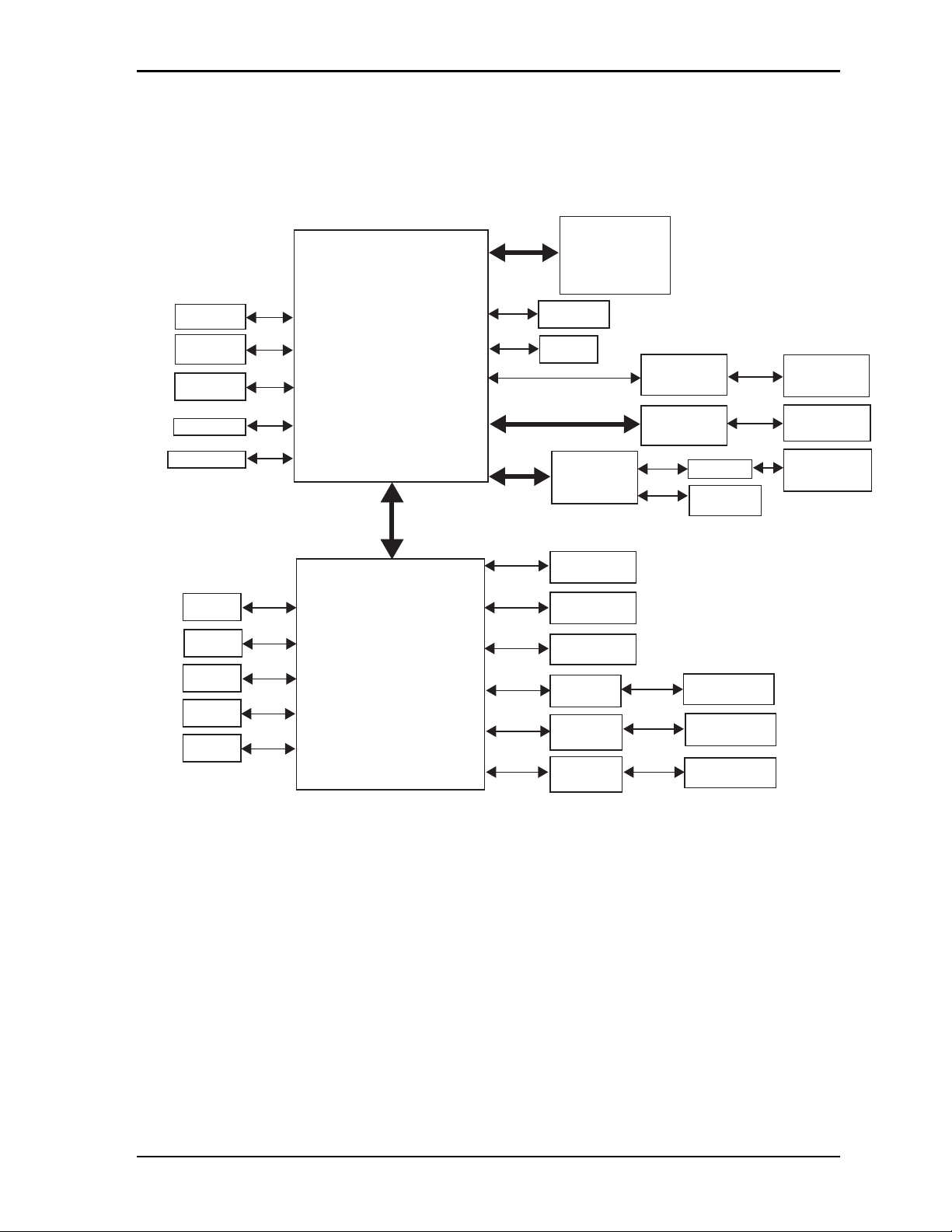
CM720BlkDiag_b
PC/104
LPC to ISA
Connector
Bridge
F85226FG
PCIe to PCI
Bridge
PLX PEX8112
CPU
Intel Atom E620T, E660T, or E680T
(600MHz, 1.3GHz, or 1.6GHz)
with integrated
Processor Core and
Graphics Memory Controller Hub
PC/104-Plus
Connector
PCH EG20T
(Platform Controller Hub)
Intel CS82TPCF
LVDS Header
SDVO
Connector
Memory Bus
ISA Bus
PCI Bus
CAN
Header
COM0
Header
RS-232
Transceiver
LPC Bus
PCIe Bus (Port 1)
PCIe Bus (Port 0)
USB
Header
USB
Header
USB (2)
USB
Header
USB (2)
USB (2)
Serial 1
Serial 2
SPI Flash
GPIO
Header
SATA 0
SATA 1
SPI
SMBus
Temperature
Monitor
GPIO
I2C
Header
I2C
SMBus
Header
Utility Header
Battery Header
Solid State
Drive
SDIO
SD Socket
SATA 0
Connector
RS-232
Transceiver
CAN
Transceiver
CAN
COM1, 2, 3
Header
Magnetics
Ethernet LED
Header
Gigabit Ethernet
Controller
82574IT
Gigabit Ethernet
Header
MDI
PCIe Bus
(Port 2)
4x DDR2
System Memory 1
4x DDR2
System Memory 2
Logo Screen (Splash)
Block Diagram
Figure 2-2 shows the functional components of the CoreModule 720.
CoreModule 720 Reference Manual 7
Figure 2-2. Functional Block Diagram
Page 14

Chapter 2 Product Overview
Major Component (ICs) Definitions
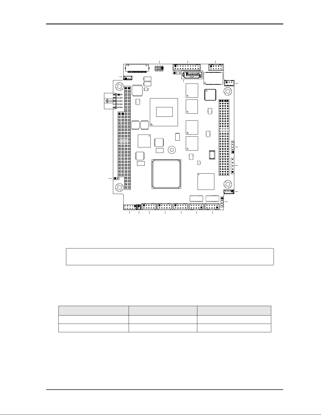
Table 2 -1 lists the major ICs, including a brief description of each, on the CoreModule 720. Figures 2-3 and
2-4 show the locations of the major ICs.
Table 2-1. Major Component Descriptions and Functions
Chip Type Mfg. Model Description Function
CPU (U1) Intel Atom E620T, E660T,
or E680T
DDR2 Memory - 1
(U2, U3, U4, U5)
DDR2 Memory - 2
(U6, U7, U8, U9 - on
bottom side [see
Figure 2-4])
PCH [Platform
Controller Hub
(U10)]
CAN Transceiver
(U12 - on bottom
side [see Figure 2-4])
Gigabit Ethernet
Controller (U15)
Ethernet EEPROM
(U16)
LPC-to-ISA Bridge
(U17 - on bottom
side [see Figure 2-4])
PCIe-to-PCI Bridge
(U18)
Micron MT47H256M8EB-25E On-board DDR2
Micron MT47H256M8EB-25E On-board DDR2
Intel CS82TPCF
(PCH EG20T)
Texas
Instruments
Intel 82574IT Gigabit Ethernet
Atmel AT25128B-SSHL-B Three-Wire Serial
Fintek F85226FG LPC-to-ISA
PLX
Technology
SN65HVD1040D Transceiver for
PEX8112 PCIe-to-PCI
600MHz, 1.3GHz,
or 1.6GHz processor
with 8-way L2 cache
System Memory - 1
System Memory - 2
I/O Hub for
common user
interfaces
Controller Area
Network (CAN)
controller
EEPROM for
Gigabit Ethernet
Controller
interface
interface
Integrates
Processor Core
and Graphics
Memory
Controller Hub
Provides highspeed data
transfer
Provides highspeed data
transfer
Provides
Southbridge
interfaces and
off loads some
Northbridge
functions from
the CPU
Provides up to
1 Mbps of
differential
transmit and
receive
capabilities for
the CAN
controller in the
PCH
Generates PCIe
10T/100TX/
1000T Ethernet
signals
Provides storage
for MAC
addresses, serial
numbers, and
pre-boot
configuration
data
Migrates legacy
ISA interfaces
Migrates legacy
PCI interfaces
8 Reference Manual CoreModule 720
Page 15

Chapter 2 Product Overview
Table 2-1. Major Component Descriptions and Functions (Continued)
SPI EEPROM (U20 on bottom side [see
Figure 2-4])
RS-232 Transceiver
(U21)
Atmel AT25640B-SSHL Electronically-
erasable
programmable readonly memory
Maxim MAX3245EEUI+ Transceiver for
Serial 1 RS-232
signals
Stores PCIe-toPCI bridge
configuration
data
Transmits and
receives RS-232
signals for
COM0
RS-232 Transceiver
(U22)
Maxim MAX3245EEUI+ Transceiver for
Serial 2 RS-232
signals
Transmits and
receives RS-232
signals for
COM1, 2, & 3
SPI Flash (U31) PCT PCT25VF016B-75-4I-
S2AF
Serial Peripheral
Interface Flash
Stores BIOS in
Flash Memory
Memory chip (for
firmware)
Thermal Regulator PCIe-to-PCI Bridge
(U32 - on bottom
side [see Figure 2-4])
AME AME8850AEEVADJZ Linear Regulator Provides power-
saving mode,
over-current
protection, and
thermal
shutdown for the
PCIe-to-PCI
Bridge
Temperature Monitor
(U33)
ON
Semicondu
ctor
ADM1032ARMZ Digital thermometer
for CPU temperature
Measures the
temperature
output of the
CPU and
provides over-
temperature
alarm
Thermal Regulator SSD (U35)
AME AME8850AEEVADJZ Linear Regulator Provides power-
saving mode,
over-current
protection, and
thermal
shutdown for the
Solid State
Drive
Solid State Drive
[SSD] - SATA (U37 on bottom side [see
Figure 2-4])
Transformer Gigabit Ethernet
(T1)
Greenliant GLS85LS1008P Industrial-grade,
soldered solid state
storage module
Wurth
Elektronik
7490200110 Gigabit Ethernet
Magnetics
Provides solid
state storage
through the
SATA1 port
Provides
electrical
isolation for
Gigabit Ethernet
controller
CoreModule 720 Reference Manual 9
Page 16
Chapter 2 Product Overview
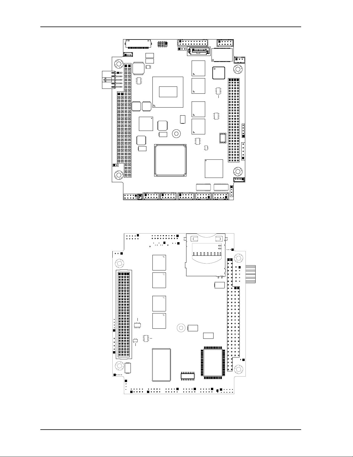
CM720_Top_Comp_a
Key:
U1 - CPU
U2 - DDR2 SDRAM - 1
U3 - DDR2 SDRAM - 1
U4 - DDR2 SDRAM - 1
U5 - DDR2 SDRAM - 1
U10 - PCH
U15 - Gigabit Ethernet Controller
U16 - Ethernet EEPROM
U18 - PCIe to PCI Bridge
U21 - RS-232 Transceiver - COM0
U22 - RS-232 Transceiver - COM1-3
U31 - SPI Flash - BIOS
U33 - Temperature Monitor
U35 - Thermal Regulator - SSD
T1 - Gigabit Ethernet Transformer
U16
U31
U15
U3
U2
U4
U18
U22
U21
U35
U10
U5
T1
U1
U33
CM720_Bottom_Comp_a
Key:
U6 - DDR2 SDRAM - 2
U7 - DDR2 SDRAM - 2
U8 - DDR2 SDRAM - 2
U9 - DDR2 SDRAM - 2
U12 - CAN Transceiver
U17 - LPC-to-ISA Bridge
U20 - SPI EEPROM - PCIe to PCI
U32 - Thermal Regulator - PCIe to PCI
U37 - Solid State Drive (SSD) - SATA
J5 - SD (Security Digital) Memory Card
Socket (See Header, Connector, and Socket table)
U9
U8
U7
U6
U12
U32
U17
U37
J5
U20
10 Reference Manual CoreModule 720
Figure 2-3. Component Locations (Top Side)
Figure 2-4. Component Locations (Bottom Side)
Page 17

Chapter 2 Product Overview
Header, Connector, and Socket Definitions
Table 2 -2 describes the headers, connectors, and socket of the CoreModule 720 shown in Figure 2-6.
Table 2-2. Module Header and Connector Descriptions
Header # Board
Access
J1 – LPC Debug Top 10-pin, 0.050" (1.27mm) female debug port header for issues such
J3 – GPIO Top 10-pin, 0.079" (2mm) header for General Purpose IO signals
J4 – CAN Top 4-pin, 0.079" (2mm) header for transmitting and receiving
J5 – SD Memory Socket Bottom
(See
Figure 2-4)
2
C
J6 – I
J7 – SATA0 Top 7-pin, 0.050" (1.27mm) standard connector for SATA devices
J8 – Ethernet - Gigabit Top 10-pin, 0.079" (2mm) shrouded header for Gigabit Ethernet port
J9 – LED Ethernet Gigabit
J10 – Serial 1 Top 10-pin, 0.079" (2mm) shrouded header for the COM0 signals
J11 – Serial 2 Top 10-pin, 0.079" (2mm) shrouded header for the COM1, 2, and 3
J12 – USB 0-1 Top 10-pin, 0.079" (2mm) shrouded header for USB0 and USB1
J13 – USB 4-5 Top 10-pin, 0.079" (2mm) shrouded header for USB4 and USB5
J14 – USB 2-3 Top 10-pin, 0.079" (2mm) shrouded header for USB2 and USB3
J15 – SDVO Top 30-pin, 0.020" (0.5mm) flip-lock, bottom-contact FPC connector
J17 – PC/104-Plus Top/Bottom 120-pin, 0.079" (2mm) standard connector for PC/104-Plus
J18 – PC/104 Top/Bottom 104-pin, 0.100" (2.54mm) standard connector for PC/104 signals
J19 – Power Top 10-pin, 0.100" (2.54mm) right-angle, shrouded header for external
J20 – Battery Top 2-pin, 0.049" (1.25mm) shrouded header for power from external
J21 – Fan Top 3-pin, 0.079" (2mm) shrouded header for System Fan signals
Top
Top 4-pin, 0.049" (1.25mm) shrouded header for Ethernet LED signals
Description
as Port 80 POST errors (NELTRON, 2200SB-10G-SM-23-CR)
(TEKA, HM205CB1N-191-00)
Controller Area Network signals
(JIH VEI, 21N12050-04S10B-01G-4/2.8-G)
9-pin standard socket for Security Digital Memory cards
(TYCO, 1939115-1)
5-pin, 0.079" (2mm) header for I2C bus (SAMTEC, TMM-10503-LM-S)
(WIN WIN, WATM-07DBN4B3B8UW)
(HIROSE, DF11-10DP-2DSA)
(SMP, W125-0410-310-Z)
(HIROSE, DF11-10DP-2DSA)
signals (HIROSE, DF11-10DP-2DSA)
signals (HIROSE, DF11-10DP-2DSA)
signals (HIROSE, DF11-10DP-2DSA)
signals (HIROSE, DF11-10DP-2DSA)
for single-channel SDVO interface (HIROSE, FH12-30S-0.5SH)
signals (EPT, 264-60303-12)
(COMM CON, 51923G)
power connection (FCI, 78207-210HLF)
battery (SMP, W125-0210-310-Z)
(NELTRON, 2417SJ-03)
CoreModule 720 Reference Manual 11
Page 18
Chapter 2 Product Overview
1
234
5
678910
10-pin, two rows,
Odd/Even, (1, 2)
CM720_ConNum_a
Table 2-2. Module Header and Connector Descriptions (Continued)
J22 – Utility Top 5-pin, 0.100" (2.54mm) single-row header for Power Button,
Reset Switch, and Speaker signals
(SAMTEC, HMTSW-105-08-LM-S-300)
J23 – LVDS Top 20-pin, 0.079" (2mm) shrouded header for LVDS video signals
(HIROSE, DF11-20DP-2DSA)
J24 – SMBus Top 5-pin, 0.079" (2mm) single-row header for SMBus signals
(SMP, W125-0510-310-Z)
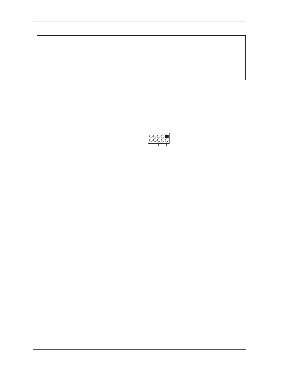
NOTE The pinout tables in Chapter 3 of this manual identify pin sequence using the
following method: A 10-pin header with two rows of pins, using odd/even
numbering, where pin 2 is directly across from pin 1, is noted as 10-pin, 2 rows, odd/
even (1, 2). See Figure 2-5.
Figure 2-5. Connector Pin Sequences
12 Reference Manual CoreModule 720
Page 19
Chapter 2 Product Overview
CM720_Top_Conn_a
Key:
J1 - LPC
J3 - GPIO
J4 - CAN
J5 - SD Memory Socket - Bottom
J6 - I2C
J7 - SATA0
J8 - Ethernet - Gigabit
J9 - Ethernet LED - Gigabit
J10 - Serial 1 - COM 0
J11 - Serial 2 - COM 1, 2, 3
J12 - USB 0, 1
J13 - USB 4, 5
J14 - USB 2, 3
J15 - SDVO
J17 - PC/104-Plus
J18 - PC/104
J19 - Power
J20 - Battery
J21 - Fan
J22 - Utility
J23 - LVDS
J24 - SMBus
JP1 - RTC Reset
(See jumper table)
JP3 - LVDS Voltage Select
(See jumper table)
J21
J13J20 J12 J10J14 J11
J7
DC
AB
ABCD
JP3
JP1
J23
J6
J22
J24
J3
J19
J9
J1
J8
J15
J4
J17
J18
Jumper Header Definitions
Table 2 -3 describes the jumper headers shown in Figure 2-7. Both jumper headers provide 0.079" (2mm)
pitch.
Table 2-3. Jumper Settings
Figure 2-6. Header, Connector, and Socket Locations (Top Side)
NOTE Black square pins on headers and connectors represent pin 1. Black square pins on
right-angle headers represent pin 2 in top-side views and pin 1 in bottom-side views.
Jumper Header Installed Removed
JP1 – Clear CMOS Enable Disable (Default)
JP3 – LVDS Voltage Selection Enable +3.3V (1-2) (Default) Enable +5V (2-3)
CoreModule 720 Reference Manual 13
Page 20

Chapter 2 Product Overview
CM720_Top_Jmpr_a
Key:
JP1 - Clear CMOS
JP3 - LVDS Voltage Select
JP3
JP1
Figure 2-7. Jumper Header Locations (Top Side)
Specifications
Physical Specifications
Table 2 -4 provides the physical dimensions of the CoreModule 720.
Table 2-4. Weight and Footprint Dimensions
Item Dimension
Weight 0.12 kg (0.25 lbs)
Height (overall) 11.05 mm (0.435 inches)
Board thickness 2.362 mm (0.093 inches)
Width 96.01 mm (3.78 inches)
Length 115.57 mm (4.55 inches)
NOTE Height is measured from the upper
board surface to the highest permanent
component (PC/104 connector) on the
upper board surface. This does not
include the cooling solution, which is
required on all versions of the board and
may increase the height of the board.
On-board component height should not
exceed 0.345" (8.763mm) from the
upper surface of the board and 0.190"
(4.826mm) from the lower surface of the
board. See Figure 2-10 on page 18 for
the stack heights of the cooling solutions
on the board.
14 Reference Manual CoreModule 720
Page 21

Chapter 2 Product Overview
CM720_Top_Dmn_a
0.00
0.00
0.20 (5.08mm)
0.50 (12.70mm)
1.38 (35.05mm)
3.35 (85.09mm)
3.55 (90.17mm)
4.05 (102.87mm)
3.55 (90.17mm)
3.20 (81.28mm)
0.30 (7.62mm)
0.50 (12.70mm)
0.20 (5.08mm)
0.33 (8.38mm)
1.95 (49.53mm)
3.45 (87.63mm)
3.58 (90.93mm)
3.78 (96.01mm)
0.00
Mechanical Specifications
Figure 2-8. Mechanical Overview (Top Side)
NOTE All dimensions are given in inches. Black square pins on headers and connectors
represent pin 1. Black square pins on right-angle headers represent pin 2 in top-side
views and pin 1 in bottom-side views.
CoreModule 720 Reference Manual 15
Page 22

Chapter 2 Product Overview
Power Specifications
Table 2 -5 provides the current measurements for the CoreModule 720.
Table 2-5. Power Supply Requirements
Parameter 600MHz E620T
Characteristics
Input Type Regulated DC voltages Regulated DC voltages Regulated DC voltages
In-rush Peak Current and
Duration
Typical Idle Current 1.67A (8.34W) 1.69A (8.43W) 1.67A (8.33W)
BIT Current 2.72A (13.61W) 2.85A (14.25W) 2.97A (14.85W)
Operating configurations:
See Figure 2-9 See Figure 2-9 See Figure 2-9
1.3GHz E660T
Characteristics
1.6GHz E680T
Characteristics
• In-rush operating configuration includes CRT monitor, 2GB memory, 8GB SSD, and power.
• Idle operating configuration includes In-rush configuration as well as one SATA hard drive, USB mouse
and keyboard.
• BIT (Burn-In-Test) operating configuration includes Idle configuration as well as four USB loop backs,
four serial ports with loop backs, and one Ethernet connection.
Figure 2-9. E6XXT Peak In-Rush Current and Duration
16 Reference Manual CoreModule 720
Page 23

Chapter 2 Product Overview
Environmental Specifications
Table 2 -6 provides the most efficient operating and storage condition ranges required for this module.
Table 2-6. Environmental Requirements
Parameter Conditions
Temperature
Standard –20° to +70° C (–4° to +158° F)
Extended (Optional) –40° to +85° C (–40° to +185° F)
Storage –55° to +85° C (–67° to +185° F)
Humidity
Operating 5% to 90% relative humidity, non-condensing
Non-operating 5% to 95% relative humidity, non-condensing
CoreModule 720 Reference Manual 17
Page 24

Chapter 2 Product Overview
0.39
0.44
0.20
0.09
CM720_Cooling_Assy_hts_b
0.09
1.18
2.66
0.98
0.32
2.46
Active Heatsink
CoreModule 720
Fan
1.48
0.39
0.44
Passive Heatsink
CoreModule 720
Thermal/Cooling Requirements
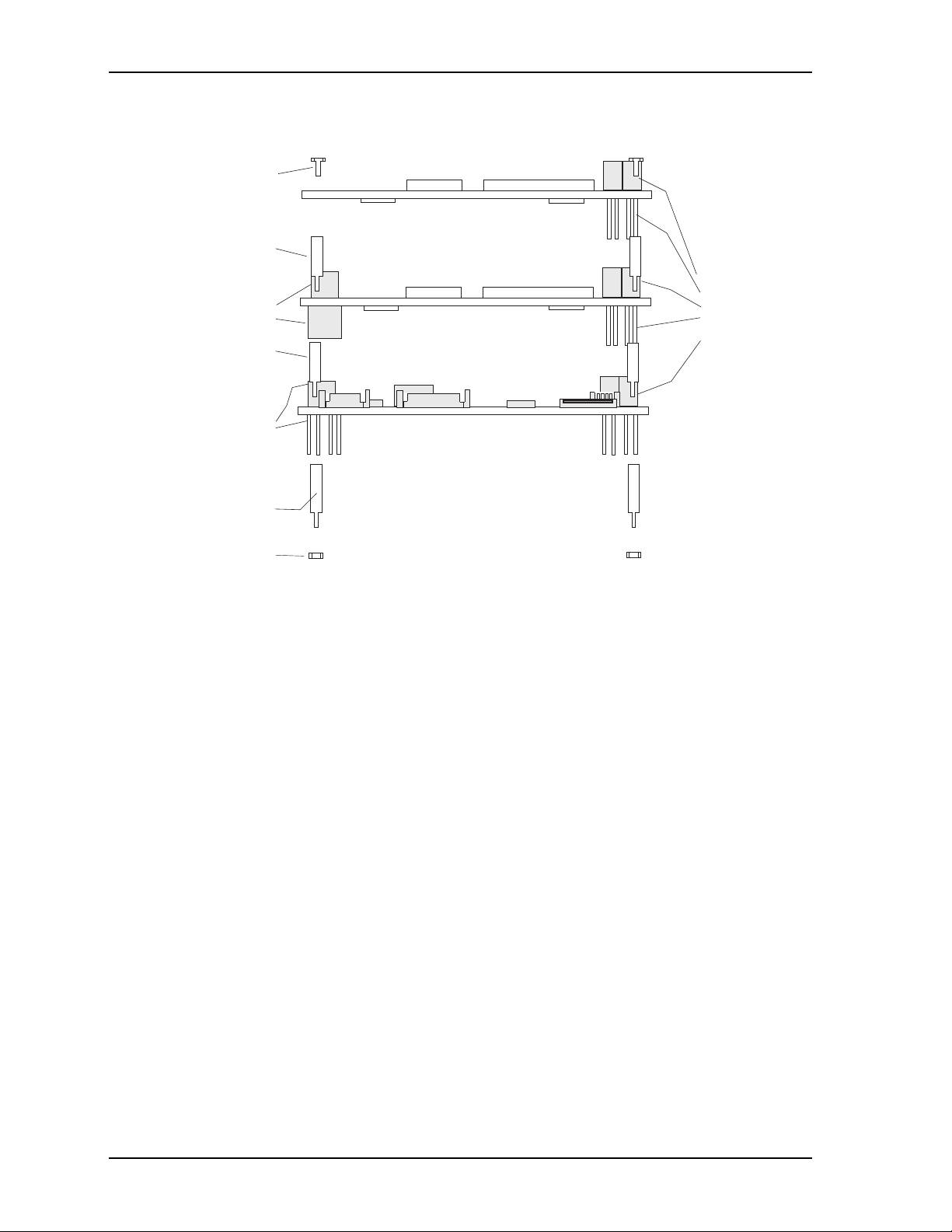
The CPU is the primary source of heat on the board. The CoreModule 720 is designed to operate at the
maximum speed of the CPU and requires a cooling solution (available option). See Tab le 2-7 for optional
cooling solution temperature qualifications. Figure 2-10 depicts height measurements of the optional
cooling assemblies.
Table 2-7. ADLINK Optional Cooling Solutions
Cooling Solution Description
Passive Heatsink - Copper
(without fan)
Passive Heatsink - Aluminum
(without fan)
Active Heatsink
(with fan)
Qualified to maintain optimal performance between -40°C and +85°C.
(Note: The E680T CPU is qualified only for -20°C to +70°C with a
copper heatsink.)
Qualified to maintain optimal performance between -20°C and +70°C.
(Note: The E680T CPU is not qualified to use an aluminum heatsink.)
Qualified to maintain optimal performance between -40°C and +85°C.
(Note: The E680T CPU requires an active heatsink for temperatures
between +70°C and +85°C.)
Figure 2-10. Stack Heights of Cooling Assemblies
NOTE All heights are given in inches. Copper and aluminum passive cooling
assemblies share the same height measurements.
18 Reference Manual CoreModule 720
Page 25

Chapter 3 Hardware
Overview
This chapter discusses the chips and connectors of the module features in the following order:
• CPU
• Graphics
• Memory
• Interrupt Channel Assignments
• Memory Map
• I/O Address Map
• Serial Port Interfaces
• USB Interfaces
• Ethernet Interface
• Video Interfaces
LV DS
SDVO (Supports VGA as described in Appendix B, “Video Adapter Board ” )
• Power Interface
• GPIO Interface
• Utility Interface
Power Button
Reset Switch
Speaker
• SMBus Interface
• CAN (Controller Area Network) Interface
2
• I
C Interface
• System Fan Interface
• Battery Interface
• Ethernet LED Interface
• Miscellaneous
SSD (SATA Solid State Drive)
Time of Day/RTC
Oops! Jumper (BIOS Recovery)
Serial Console
Hot Cable
Watchdog Timer
CoreModule 720 Reference Manual 19
Page 26

Chapter 3 Hardware
NOTE ADLINK Technology, Inc. only supports the features and options listed in this
manual. The main components used on the CoreModule 720 may provide more
features or options than are listed in this manual. Some of these features and
options are not supported on the module and will not function as specified in the
chip documentation.
The pin-out tables only of non-standard headers and connectors are included in
this chapter. This chapter does not include pin-out tables for standard headers,
connectors, and sockets such as SATA, SD memory, PC/104, and PC/104-Plus.
Refer to references in Chapter 1 for PC/104 and PC/104 Plus pin outs.
CPU
The CoreModule 720 offers three versions of the Intel Atom E6XXT CPU—the E620T, E660T, and
E680T—operating at 600MHz, 1.3GHz, and 1.6GHz, respectively. The E6XXT integrates a highperformance x86 Processor Core with Memory Controller and 3D Graphics Engine. This single chip is
based on 45-nm process technology and provides an open-standard PCI Express v1.0 interface, supporting
user-defined PCH, ASIC, FPGA, and off-the-shelf discrete components, ideal for deeply embedded
applications.
Graphics
The E6XXT CPU provides a 2D/3D graphics engine that performs pixel shading and vertex shading within
a single hardware accelerator, which minimizes access to memory and improves render performance.
Memory
The CoreModule 720 employs two ranks of four system DRAM memory chips, which provide up to 2GB of
extended memory, supporting aggressive power management to reduce power consumption, shallow selfrefresh and a new deep self-refresh, proactive page closing policies to close unused pages, and partial writes
through data mask pins.
20 Reference Manual CoreModule 720
Page 27

Chapter 3 Hardware
Interrupt Channel Assignments
The interrupt channel assignments are shown in Table 3-1.
Table 3-1. Interrupt Channel Assignments
Device vs IRQ No. 0 1 2 3 4 5 6 7 8 9 10 11 12 13 14 15
Timer X
Secondary Cascade X
COM0 Automatically Assigned
COM1 Automatically Assigned
COM2 Automatically Assigned
COM3 Automatically Assigned
RTC X
Math Coprocessor X
PCI INTA Automatically Assigned
PCI INTB Automatically Assigned
PCI INTC Automatically Assigned
PCI INTD Automatically Assigned
USB Automatically Assigned
Video Automatically Assigned
Legend: D = Default, O = Optional, X = Fixed
NOTE The IRQs for USB and Video are automatically assigned by the BIOS Plug and
Play logic. Local IRQs assigned during initialization can not be used by external
devices.
Memory Map
The following table provides the common PC/AT memory allocations. These are DOS-level addresses. The
OS typically hides these physical addresses by way of memory management.
Table 3-2. Memory Map
Base Address Function
00000000h - 0009FFFFh Conventional Memory
000A0000h - 000AFFFFh Graphics Memory
000B0000h - 000B7FFFh Mono Text Memory
000B8000h - 000BFFFFh Color Text Memory
000C0000h - 000CFFFFh Standard Video BIOS
000D0000h - 000DFFFFh DVMT Memory
000E0000h - 000EFFFFh PCI Express Base Memory
000F0000h - 000FFFFFh System Flash and PCI Resources
CoreModule 720 Reference Manual 21
Page 28

Chapter 3 Hardware
I/O Address Map
Table 3 -3 shows the I/O address map. These are DOS-level addresses. The OS typically hides these physical
addresses by way of memory management.
Table 3-3. I/O Address Map
Address (hex) Subsystem
0000-00F Primary DMA Controller
0020-0021 Master Interrupt Controller
0040-0043 Programmable Interrupt Timer (Clock/Timer)
0060-006F Keyboard Controller
0070-007F CMOS RAM, NMI Mask Reg, RT Clock
0080-009F DMA Page Registers
00A0-00BF Slave Interrupt Controller
00C0-00DF Slave DMA Controller #2
00F0-00FF Math Coprocessor
03B0-03BB Video (monochrome)
03C0-03DF VGA
0400-041F SMBus Configuration Ports
0500-053F PCH GPIO Configuration Ports
0800-087F PCH Power Management Ports
0A79h ISA PnP Ports
0CF8-0CFF PCI bus Configuration Address and Data
NOTE 0A79h is the ISA PnP port used by the BIOS and an OS that supports this feature to
recognize ISA PnP (Plug and Play) cards.
The Intel I/O hub PCH EG20T does not support ISA DMA.
22 Reference Manual CoreModule 720
Page 29

Chapter 3 Hardware
Serial Interfaces
The CoreModule 720 provides four RS-232 serial ports. The PCH EG20T contains the circuitry for all four
serial ports and delivers the signals through two RS-232 transceivers: one transceiver for port COM0 and the
second transceiver for ports COM1, COM2, and COM3. The serial ports support the following features:
• One individual high-speed NS16C550A-compatible UART (COM0)
• Programmable word length, stop bits, and parity
• 16-bit programmable baud rate generator and Interrupt generator
• Loop-back mode
• Four individual 16-bit FIFOs
• Serial Port Headers
J10 - Serial 1 (COM0) supports RS-232 and full modem
J11 - Serial 2 (COM1, COM2, and COM3) supports RS-232
Table 3 -4 defines the pins and corresponding signals for serial 1 header (J10), which each consist of 10 pins,
2 rows, odd/even sequence (1, 2), and 0.079" (2mm) pitch.
Table 3-4. Serial 1 (COM0) Interface Pin Signal Descriptions (J10)
Pin # Signal DB9
Pin #
1 S0_DCD* 1 COM0 Data Carrier Detect – Indicates external serial device is detecting
2 S0_DSR* 6 COM0 Data Set Ready – Indicates external serial device is powered,
3 S0_RXD 2 COM0 Receive Data – Serial port receive data input is typically held at a
4 S0_RTS* 7 COM0 Request To Send – Indicates serial port is ready to transmit data.
5 S0_TXD 3 COM0 Transmit Data – Serial port transmit data output is typically held
6 S0_CTS* 8 COM0 Clear To Send – Indicates external serial device is ready to
7 S0_DTR* 4 COM0 Data Terminal Ready – Indicates serial port is powered,
8 S0_RI* 9 COM0 Ring Indicator – Indicates external serial device is detecting a
9
10 Key/NC NC Key Pin/Not connected
GND 5 Ground
Description
a carrier signal (i.e., a communication channel is currently open). In
direct connect environments, this input is driven by DTR as part of the
DTR/DSR handshake.
initialized, and ready. Used as hardware handshake with DTR for overall
readiness.
logic 1 (mark) when no data is being transmitted, and is held “Off” for a
brief interval after an “On” to “Off” transition on the RTS line to allow
the transmission to complete.
Used as hardware handshake with CTS for low level flow control.
to a logic 1 when no data is being sent. Typically, a logic 0 (On) must be
present on RTS, CTS, DSR, and DTR before data can be transmitted on
this line.
receive data. Used as hardware handshake with RTS for low level flow
control.
initialized, and ready. Used as hardware handshake with DSR for overall
readiness.
ring condition. Used by software to initiate operations to answer and
open the communications channel.
Note: The shaded table cell denotes ground.
CoreModule 720 Reference Manual 23
Page 30

Chapter 3 Hardware
Table 3 -5 describes the pin signals of the serial 2 header (J11), which consists of 10 pins, two rows, odd/even
(1, 2) pin sequence, and 0.079" (2mm) pitch
Table 3-5. Serial 2 (COM1, 2, and 3) Interface Pin Signal Descriptions (J11)
Pin # Signal DB9
Pin #
1 S1_TXD 3 COM1 Transmit Data – Serial port transmit data output is typically held
2 S1_RXD 2 COM1 Receive Data – Serial port receive data input is typically held at a
3
4 S2_TXD 3 COM2 Transmit Data – Serial port transmit data output is typically held
5 S2_RXD 2 COM2 Receive Data – Serial port receive data input is typically held at a
6
7 S3_TXD 3 COM3 Transmit Data – Serial port transmit data output is typically held
8 S3_RXD 2 COM3 Receive Data – Serial port receive data input is typically held at a
9
10
Note: The shaded table cells denote ground.
GND 5 Ground
GND 5 Ground
GND 5 Ground
GND N/A Ground
Description
to a logic 1 when no data is being sent.
logic 1 (mark) when no data is being transmitted.
to a logic 1 when no data is being sent.
logic 1 (mark) when no data is being transmitted.
to a logic 1 when no data is being sent.
logic 1 (mark) when no data is being transmitted.
USB Interfaces
The CoreModule 720 contains three root USB hubs and six functional USB ports. The PCH provides the
USB function including the following features:
• Supports USB v.2.0 EHCI and USB v.1.1 UHCI
• Provides over-current detection status
• Provides a fuse on board for over-current protection
Table 3 -6 describes the pin signals of the USB0 and USB1 header which consists of 10 pins, in two rows,
with odd/even (1, 2) pin sequence, and 0.079" (2mm) pitch.
Table 3-6. USB0 and USB1 Interface Pin Signals (J12)
Pin # Signal Description
1
2
3 CONN_USB0_N USB0 Port Data Negative
4 CONN_USB1_N USB1 Port Data Negative
5 CONN_USB0_P USB0 Port Data Positive
6 CONN_USB1_P USB1 Port Data Positive
7
8
USB-PWR_0 USB0 Power – VCC (+5V +/-5%) power goes to the port through an on
board fuse. Port is disabled if this input is low.
USB-PWR_1 USB1 Power – VCC (+5V +/-5%) power goes to the port through an on
board fuse. Port is disabled if this input is low.
USB_GND0 USB0 Ground
USB_GND1 USB1 Ground
24 Reference Manual CoreModule 720
Page 31

Chapter 3 Hardware
Table 3-6. USB0 and USB1 Interface Pin Signals (J12) (Continued)
9
10
USB_GND0 USB0 Ground
USB_GND1 USB1 Ground
Note: The shaded table cells denote power or ground.
Table 3 -7 describes the pin signals of the USB2 and USB3 header, which consists of 10 pins in two rows,
with odd/even (1, 2) pin sequence, and 0.079" (2mm) pitch.
Table 3-7. USB2 and USB3 Interface Pin Signals (J14)
Pin # Signal Description
1
USB-PWR_2 USB2 Power – VCC (+5V +/-5%) power goes to the port through an on
board fuse. Port is disabled if this input is low.
2
USB-PWR_3 USB3 Power – VCC (+5V +/-5%) power goes to the port through an on
board fuse. Port is disabled if this input is low.
3 CONN_USB2_N USB2 Port Data Negative
4 CONN_USB3_N USB3 Port Data Negative
5 CONN_USB2_P USB2 Port Data Positive
6 CONN_USB3_P USB3 Port Data Positive
7
8
9
10
USB_GND2 USB2 Ground
USB_GND3 USB3 Ground
USB_GND2 USB2 Ground
USB_GND3 USB3 Ground
Note: The shaded table cells denote power or ground.
Table 3 -8 describes the pin signals of the USB4 and USB5 header, which consists of 10 pins in two rows,
with odd/even (1, 2) pin sequence, and 0.079" (2mm) pitch.
Table 3-8. USB4 and USB5 Interface Pin Signals (J13)
Pin # Signal Description
1
USB-PWR_4 USB4 Power – VCC (+5V +/-5%) power goes to the port through an on
board fuse. Port is disabled if this input is low.
2
USB-PWR_5 USB5 Power – VCC (+5V +/-5%) power goes to the port through an on
board fuse. Port is disabled if this input is low.
3 CONN_USB4_N USB4 Port Data Negative
4 CONN_USB5_N USB5 Port Data Negative
5 CONN_USB4_P USB4 Port Data Positive
6 CONN_USB5_P USB5 Port Data Positive
7
8
9
10
USB_GND4 USB4 Ground
USB_GND5 USB5 Ground
USB_GND4 USB4 Ground
USB_GND5 USB5 Ground
Note: The shaded table cells denote power or ground.
CoreModule 720 Reference Manual 25
Page 32

Chapter 3 Hardware
Ethernet Interface
The CoreModule 720 supports one Gigabit Ethernet interface. The Ethernet interface is implemented from
the 82574IT Ethernet controller and provides one GLAN interface, which occupies PCI Express port 2. The
Ethernet function supports multi-speed operation at 10/100/1000 Mbps and operates in full-duplex at all
supported speeds or half duplex at 10/100 Mbps while adhering to the IEEE 802.3x flow control
specification. The Ethernet interface offers the following features:
• Full duplex or half duplex support at 10 Mbps, 100 Mbps, or 1000 Mbps
• In full duplex mode, the Ethernet controller adheres to the IEEE 802.3x Flow Control specification
• In half duplex mode, performance is enhanced by a proprietary collision reduction mechanism
• IEEE 802.3 compatible physical layer to wire transformer
• IEEE 802.3u Auto-Negotiation support
• Fast back-to-back transmission support with minimum interframe spacing (IFS)
• IEEE 802.3x auto-negotiation support for speed and duplex operation
• On-board magnetics (Ethernet isolation transformer)
Table 3 -9 describes the pin signals of the Ethernet interface, which consists of a two-row, 10-pin shrouded
header in two rows of odd/even (1,2) pin sequence, and 0.079" (2mm) pitch.
Table 3-9. Ethernet Interface Pin Signal Descriptions (J8)
Pin # Signal Description
1
2
3 MDI0+ Media Dependent Interface 0 +/-
4MDI0-
5 MDI1+ Media Dependent Interface 1 +/-
6MDI1-
7 MDI2+ Media Dependent Interface 2 +/-
8MDI2-
9 MDI3+ Media Dependent Interface 3 +/-
10 MDI3-
Note: The shaded table cells denote ground.
GND Ground
GND
NOTE The magnetics (isolation transformer, T1) for the Ethernet connector is included
on the CoreModule 720.
26 Reference Manual CoreModule 720
Page 33

Chapter 3 Hardware
Video (SDVO/LVDS) Interfaces
The Atom™ E6XXT CPU provides an integrated 2D/3D graphics engine, which supports video decode such
as MPEG2, MPEG4, VC1, WMV9, H.264 (main, baseline at L3 and High-profile level 4.0/4.1), and DivX*
as well as video encode such as MPEG4, H.264 (baseline at L3), and VGA. The CPU supports LVDS and
SDVO display ports, permitting simultaneous, independent operation of two displays. The video interface
features are listed in the following bullets. Refer to Table 3-10 for definitions of the SDVO pin signals and
Table 3-11 for the LVDS pin signal definitions.
SDVO:
• Supports a maximum resolution of 1280 x 1024 at 85Hz (pixel clock rate up to 160MHz)
• Supports a single channel interface through a 30-pin FPC connector
• Supports 100MHz to 160MHz derivative clock frequency
• Supports third-party output formats such as DVI, LVDS, HDMI, TV-Out, and VGA
• Provides a control bus able to operate at up to 1 MHz
LVDS:
• Supports a maximum resolution of 1280 x 768 at 60Hz (pixel clock rate up to 80MHz)
• Supports minimum pixel clock rate of 19.75MHz
• Supports a single channel interface through a 20-pin header
• Supports pixel color depths of 18 and 24 bits
• Supports 20MHz to 80MHz derivative clock frequency
Table 3-10 lists the pin signals of the SDVO FPC connector, which provides 30 pins in a single row with
0.020" (0.5mm) pitch.
Table 3-10. SDVO Interface Pin Signals (J15)
Pin # Signal Description
1
2 SDVOB_CLK- SDVO B Clock Negative
3 SDVOB_CLK+ SDVO B Clock Positive
4
5 SDVOB_GREEN- SDVO B GREEN Negative
6 SDVOB_GREEN+ SDVO B GREEN Positive
7
8 SDVOB_INT- SDVO B Input Interrupt Negative
9 SDVOB_INT+ SDVO B Input Interrupt Positive
10
11 SDVOB_BLU- SDVO B BLUE Negative
12 SDVOB_BLU+ SDVO B BLUE Positive
13
14 SDVOB_RED- SDVO B RED Negative
15 SDVOB_RED+ SDVO B RED Positive
16
17 SDVO_FLDSTALL- SDVO Input Field Stall Negative
18 SDVO_FLDSTALL+ SDVO Input Field Stall Positive
19
GND1 Ground 1
GND2 Ground 2
GND3 Ground 3
GND4 Ground 4
GND5 Ground 5
GND6 Ground 6
GND7 Ground 7
CoreModule 720 Reference Manual 27
Page 34

Chapter 3 Hardware
Table 3-10. SDVO Interface Pin Signals (J15) (Continued)
Pin # Signal Description
20 SDVO_I2C_CLK I2C control signal (Clock) for SDVO device
21 SDVO_I2C_DAT I2C control signal (Data) for SDVO device
22 RESET Reset signal
23
24
25
26
+3.3V_1 +3.3 Volt Power 1
+2.5V +2.5 Volt Power
+5V_1 +5 Volt Power 1
GND8 Ground 8
27 SDVO_TVCLKIN- SDVO TV-Out Synchronization Clock Input - Negative
28 SDVO_TVCLKIN+ SDVO TV-Out Synchronization Clock Input - Positive
29
30
+3.3V_2 +3.3 Volt Power 2
+5V_2 +5 Volt Power 2
Note: The shaded table cells denote power or ground.
Table 3-11 lists the pin signals of the LVDS video header, which provides 20 pins, 2 rows, odd/even pin
sequence (1, 2) with 0.079" (2mm) pitch.
Table 3-11. LVDS Video Interface Pin Signals (J23)
Pin # Signal Description
1
2
3
4
+12V +12 volts for flat panel and backlight
VCC_LVDS_CONN JP3 determines LVDS voltage (+3.3V or +5V)
GND Ground
GND Ground
5 LVDSA_CLK_P LVDS A Clock Positive
6 LVDSA_CLK_N LVDS A Clock Negative
7 LVDSA_DAT3_P LVDS A DATA Positive Line 3
8 LVDSA_DAT3_N LVDS A DATA Negative Line 3
9 LVDSA_DAT2_P LVDS A DATA Positive Line 2
10 LVDSA_DAT2_N LVDS A DATA Negative Line 2
11 LVDSA_DAT1_P LVDS A DATA Positive Line 1
12 LVDSA_DAT1_N LVDS A DATA Negative Line 1
13 LVDSA_DAT0_P LVDS A DATA Positive Line 0
14 LVDSA_DAT0_N LVDS A DATA Negative Line 0
15 LBKLT_CTL Panel Backlight Control
16 LVDD_EN Enable Panel Power
17 LDDC_CLK Display Data Channel Clock
18 LDDC_DATA Display Data Channel Data
19 LBKLT_EN Enable Backlight Inverter
20 NC Not Connected
Note: The shaded table cells denote power or ground.
28 Reference Manual CoreModule 720
Page 35

Chapter 3 Hardware
Power Interface
The CoreModule 720 requires one +5 volt DC power source and provides a shrouded 10-pin, right-angle
header with 2 rows, odd/even pin sequence (1, 2), and 0.100" (2.54mm) pitch. If the +5VDC power drops
below ~4.65V, a low voltage reset is triggered, resetting the system.
The power input header (J19) supplies the following voltage and ground directly to the module:
• 5.0VDC +/- 5%
Table 3-12. Power Interface Pin Signals (J19)
Pin Signal Descriptions
1
2
3
4
5
6
7
8
9
10
GND Ground
+5V +5 Volts
GND Ground
+12V +12 Volts routed to PC/104, PC/104-Plus, and LVDS interfaces
GND Ground
+3.3V_PCI +3.3 Volts routed to PCI
GND Ground
+5V +5 Volts
GND Ground
+5V +5 Volts
Note: The shaded table cells denote power or ground.
User GPIO Interface
The CoreModule 720 provides GPIO pins for customer use, routing the signals from the PCH EG20T
chipset to the J3 header. An example test application and source code reside in each BSP directory of the
CoreModule 720 Support Software QuickDrive.
For instructions on using the example applications, refer to the GPIO Readme in each BSP directory of the
QuickDrive. For more information about the GPIO pin operation, refer to the PCH EG20T datasheet at:
http://download.intel.com/embedded/chipsets/datasheet/324211.pdf
Table 3-13 describes the pin signals of the GPIO interface, which consists of a 10-pin header with 2 rows,
odd/even pin sequence (1, 2), and 0.079" (2mm) pitch.
Table 3-13. User GPIO Interface Pin Signals (J3)
Pin # Signal from PCH Description
1 GPIO0 User defined
2 GPIO4 User defined
3 GPIO1 User defined
4 GPIO5 User defined
5 GPIO2 User defined
6 GPIO6 User defined
7 GPIO3 User defined
8 GPIO7 User defined
9
10
GND Ground
GND Ground
Note: The shaded table cells denote ground.
CoreModule 720 Reference Manual 29
Page 36

Chapter 3 Hardware
Utility Interface
The Utility interface provides three I/O signals on the module and consists of a 5-pin, 0.100" (2.54mm),
single-row header (J22). The E6XXT CPU drives the Power Button and Speaker signals on the Utility
interface. A separate Power Management microprocessor drives the Reset Switch signal. Table 3-14
provides the signal definitions.
• Power Button
• Reset Switch
• Speaker
Power Button
The Utility header provides a signal for an external Power Button through pins 1 and 2. The Power Button
allows the user to shut down and power on the system. To shut down the system, press and hold the Power
Button for four seconds. Press the Power Button for one second to power on the system.
Reset Switch
Pins 2 and 3 on the Utility header provide the signal for an external reset button, which allows the user to reboot the system.
Speaker
The speaker signal provides sufficient signal strength to drive an external 1W 8 “Beep” speaker at an
audible level through pins 4 and 5 on the Utility header. The speaker signal is driven from an on-board
amplifier and the CPU.
Table 3-14 describes the pin signals of the Utility interface, which provides a 5-pin, single-row header with
0.100" (2.54mm) pitch.
Table 3-14. Utility Interface Pin Signals (J22)
Pin # Signal Description
1 PWR_BTN* External Power Button (Pins 1-2)
2
3 RESET SW* External Reset Switch signal (Pins 2-3)
4
5 SPKR_CONN Speaker Output (Pins 4-5)
Note: The shaded table cells denote power or ground. The * symbol indicates the signal is Active Low.
GND Ground
5V +5 Volts Power
30 Reference Manual CoreModule 720
Page 37

Chapter 3 Hardware
System Management Bus (SMBus)
The E6XXT chip contains a host SMBus port. The host port allows the CPU access to the SMBus slave
through header, J24. The SMBus slave includes the CPU Temperature Monitor. Table 3 -15 lists the device
name and corresponding reserved binary address on the SMBus. Table 3-16 lists the SMBus pin signals on 5
pins, 1 row, 0.079" (2mm) pitch.
Table 3-15. SMBus Reserved Addresses
Component Address (Hex)
CPU Temperature Monitor 4C
Table 3-16. SMBus Pin Signals (J24)
Pin # Signal Description
1 SMB_CLK SMBus Clock
2
3 SMB_DATA SMBus Data
4
5 SMB_ALERT* SMBus Alert
GND Ground
VSM +3.3V standby voltage
Note: The shaded table cells denote power or ground. The * symbol indicates the signal is Active Low.
CAN Bus Interface
The CAN controller resides in the PCH and performs communication in accordance with the Bosch CAN
Protocol version 2.0B Active (standard and extended formats.) The CAN transceiver connects the CAN
controller to the CAN bus, and transmits and receives CAN signals to and from the CAN header (J4). The
CAN interface delivers CAN signals used for automotive, industrial automation, and medical scanning and
imaging applications. The following list describes some of the features of the CAN Bus Interface.
+/- 12 kV ESD protection
Low-current Standby mode with bus wake up: 5 A typical
Bus-fault protection of -27V to 40V
Over-temperature shutdown
Table 3-17 defines the pin signals of the CAN bus interface, which provides a 4-pin, single-row header with
0.079" (2mm) pitch.
Table 3-17. CAN Interface Pin Signals (J4)
Pin # Signal Description
1 CAN_L Dominant Low
2 CAN_H Dominant High
3
4
+5V +5 volts power
GND Ground
Note: The shaded table cells denote power or ground.
CoreModule 720 Reference Manual 31
Page 38

Chapter 3 Hardware
I2C Interface
The CoreModule 720 provides a single-channel I2C interface, which conforms to version 2.1 of the I2C bus
specification. The I2C controller resides on the EG20T PCH and operates as a master or slave device,
supporting a multi-master bus. The following list highlights the features of the I2C bus interface.
Supports delay processing of data read/write operation
Supports master and slave devices
Supports SCL generation when acting as a clock master
Supports multiple masters
Supports Low-Speed BusClock as its clock source and generates an SCL clock based on the set
value of the I2CBC register
Supports 32-byte buffering
Provides a function that generates time out in buffer mode
Table 3-18 defines the pin signals of the I
0.079" (2mm) pitch.
Table 3-18. I2C Interface Pin Signals (J6)
Pin # Signal Description
1 I2C_CLK I2C Clock
2
GND Ground
3 I2C_DATA I2C Data
4
+3.3V +3.3 volts power
5 NC Not Connected
2
C bus interface, which provides a 5-pin, single-row header with
Note: The shaded table cells denote power or ground.
System Fan
Table 3-19 lists the pin signals of the System Fan header, which provides a single row of 3 pins with 0.079"
(2mm) pitch.
Table 3-19. System Fan Pin Signals (J21)
Pin # Signal Description
1
2 NC Not Connected
3
Note: The shaded table cells denote power or ground.
+V_FAN +5.0 volts DC +/- 5%
GND Ground
32 Reference Manual CoreModule 720
Page 39

Chapter 3 Hardware
Battery
Table 3-20 lists the pin signals of the External Battery Input header for backup RTC (Real Time Clock),
which uses 2 pins with 0.049" (1.25mm) pitch.
Table 3-20. External Battery Input Header (J20)
Pin # Signal Description
1
2
Note: The shaded table cells denote power or ground. The RTC pin has an expected current draw of
~36A at room temperature. The battery is used only when power is not applied to the board.
VBAT_EXT +3.0 volts DC
GND Ground
Ethernet External LED
This header provides signals for an external LED that indicates Ethernet links and activity using a single row
of 4 pins with 0.049" (1.25mm) pitch.
Table 3-21. Ethernet External LED Pin Signals (J9)
Pin # Signal Description
1
2 ETH_ACT_LED Ethernet Activity
3 ETH_LINK100_LED Fast Ethernet Link with +3 volts power (Pins 3-4 for Bi-Color
4 ETH_LINK1000_LED Gigabit Ethernet Link
V3.3_CONN +3 volts – Provides +3 volts to external LED (Pins 1-2 for Green
LED)
LED)
Note: The shaded table cell denotes power.
Miscellaneous
SSD (Solid State Drive)
The CoreModule 720 provides an 8GB SATA SSD, which is soldered directly onto the board. For more
information refer to the SSD data sheet: http://www.greenliant.com/dotAsset/45628.pdf
Real Time Clock (RTC)
The CoreModule 720 contains a Real Time Clock (RTC). The RTC can be backed up with a battery. If the
battery is not present, a battery-free boot function in the BIOS completes the boot process and resets the
clock to the default date and time.
NOTE Some operating systems require a valid default date and time to function.
.
CoreModule 720 Reference Manual 33
Page 40

Chapter 3 Hardware
CM720_Oopsjump
Standard DB9 Serial
Port Connector (Male)
Front View
5
4
32
1
9
87
6
CM720_HotCable
Standard DB9 Serial
Port Connector (Female)
Rear View
5
4
32
1
9
8
7
6
Oops! Jumper (BIOS Recovery)
The Oops! jumper function is provided in the event the BIOS settings you have selected prevent you from
booting the system. By using the Oops! jumper you can prevent the current BIOS settings in flash from
being loaded, allowing you to boot using default settings.
Use a jumper to connect the DTR pin (4) to the RI pin (9) on Serial Port 1 (COM0) prior to boot up to
prevent the present BIOS settings from loading. After booting with the Oops! jumper in place, remove the
Oops! jumper and return to BIOS Setup. You must now load factory defaults by selecting Restore Defaults
from the Save & Exit menu. Then select Save Changes and Exit to reboot the system. Now you can modify
the default settings to your desired values. Ensure you save the changes before rebooting the system.
To convert a standard DB9 connector to an Oops! jumper, short together the DTR (4) and RI (9) pins on the
front of the connector as shown in Figure 3-1 on the Serial Port 1 DB9 connector.
Figure 3-1. Oops! Jumper Serial Port (DB9)
Serial Console
The CoreModule 720 BIOS supports the serial console (or console redirection) feature. This I/O function is
ANSI-compatible with a serial terminal or with equivalent terminal emulation software running on another
system. This can be very useful when setting up the BIOS on a production line for systems that are not
connected to a keyboard and display.
Serial Console Setup
The serial console feature is implemented by entering the serial console settings in the BIOS Setup Utility
and connecting the appropriate serial cable (a standard null modem serial cable or “Hot Cable”) between one
of the serial ports (COM0) and the serial terminal or a PC with communications software.
Hot (Serial) Cable
To convert a standard serial cable to a “Hot Cable”, short together the RTS (7) and RI (9) pins on the serial
port DB9 connector as shown in Figure 3-2.
Figure 3-2. Serial Console Jumper
Temperature Monitoring
The temperature monitoring function is performed by the ON Semiconductor, ADM1032 temperature
monitor, which takes inputs from the thermal diodes in the CPU. The ADM1032 chip uses the two-wire
SMBus interface to communicate with the other devices, taking temperature readings and issuing alerts to
the PCH when a reading surpasses over or under temperature limits. Refer to the ADM1032 data sheet for
more information at:
htt
p://www.onsemi.com/pub_link/Collateral/ADM1032-D.PDF
34 Reference Manual CoreModule 720
Page 41

Chapter 3 Hardware
Watchdog Timer
The Watchdog Timer (WDT) restarts the system if a mishap occurs, ensuring proper start up after the
interruption. Possible problems include failure to boot properly, the application software’s loss of control,
failure of an interface device, unexpected conditions on the bus, or other hardware or software malfunctions.
The WDT (Watchdog Timer) can be used both during the boot process and during normal system operation.
• During the Boot process – If the operating system fails to boot in the time interval set in the BIOS, the
system will reset.
Enable the WDT using Watchdog Timer of the Boot menu in BIOS Setup. Set the WDT for a time-out
interval in seconds, between 0 and 600, in one-second increments in the Boot Configuration screen.
Ensure you allow enough time for the boot process to complete and for the OS to boot. The OS or
application must tickle the WDT as soon as it comes up. This can be done by accessing the hardware
directly or through a BIOS call.
• During System Operation – An application can set up the WDT hardware through a BIOS call, or by
accessing the hardware directly. Some ADLINK Board Support Packages provide an API interface to
the WDT. The application must tickle the WDT in the time set when the WDT is initialized or the
system will be reset. You can use a BIOS call to tickle the WDT or access the hardware directly.
• Watchdog Code examples – ADLINK has provided source code examples on the CoreModule 720
Support Software QuickDrive illustrating how to control the WDT. The code examples can be easily
copied to your development environment to compile and test the examples, or make any desired
changes before compiling. Refer to the WDT Readme file on the CoreModule 720 Support Software
QuickDrive.
CoreModule 720 Reference Manual 35
Page 42

Chapter 3 Hardware
36 Reference Manual CoreModule 720
Page 43

Chapter 4 BIOS Setup
Introduction
This section assumes the user is familiar with general BIOS Setup and does not attempt to describe the BIOS
functions. Refer to “BIOS Setup Menus ” on page 39 in this chapter for a map of the BIOS Setup settings. If
ADLINK has added to or modified any of the standard BIOS functions, these functions will be described.
Entering BIOS Setup (Local Video Display)
To enter BIOS Setup using a local video display for the CoreModule 720:
1. Turn on the display and the power supply to the CoreModule 720.
2. Start Setup by pressing the [Del] or [F2] keys (F2 allows you to load previous settings) when the
following message appears on the boot screen.
Please wait. This will take a few seconds.
NOTE If the setting for Fast Boot is [Enabled], the system may not enter the BIOS set
up if you do not press the <Del> or <F2> keys early in the boot sequence.
3. Follow the instructions on the right side of the screen to navigate through the selections and modify any
settings.
Entering BIOS Setup (Serial Port Console)
This section describes how to enter the BIOS setup through a remote serial terminal or PC.
1. Turn on the power supply to the CoreModule 720 and enter the BIOS Setup Utility using a local video
display.
2. Ensure the BIOS feature Serial Port Console Redirection is set to [Enabled] under the Advanced menu.
3. Accept the default options or make your own selections for the balance of the Console Redirection
fields and record your settings.
4. Ensure you select the type of remote serial terminal you will be using and record your selection.
5. Select Save Changes and Exit and then shut down the CoreModule 720.
6. Connect the remote serial terminal (or the PC with communications software) to the COM0 serial port
on the CoreModule 720.
7. Turn on the remote serial terminal or PC and set it to the settings you selected in the earlier in the
procedure.
The default settings for the CoreModule 720 are:
ANSI
115200
8 bits
no parity
1 stop bit
no flow control (None)
Disabled Recorder Mode
Disabled Resolution 100x31
[80x24] for Legacy OS Redirection
CoreModule 720 Reference Manual 37
Page 44

Chapter 4 BIOS Setup
8. Restore power to the CoreModule 720.
9. Press the F2 key to enter Setup (early in the boot sequence if Fast Boot is set to [Enabled].)
If Fast Boot is set to [Enabled], you may never see the screen prompt.
10. Use the <Enter> key to select the screen menus listed in the Opening BIOS screen.
NOTE The serial console port is not hardware protected. Diagnostic software that
probes hardware addresses may cause a loss or failure of the serial console
functions.
OEM Logo Utility
The CoreModule 720 BIOS supports a graphical logo utility, which allows the user to customize the boot
screen image. The graphical image can be a company logo or any custom image the user wants to display
during the boot process. The custom image can be displayed as the first image on screen during the boot
process and remain there while the OS boots, depending on the options selected in BIOS Setup.
NOTE The Quiet Boot feature must be set to Enabled in the Boot screen of BIOS Setup
for the system to recognize the OEM Logo feature.
Logo Image Requirements
Please contact your ADLINK Sales Representative for more information on OEM Logo Utility
requirements.
38 Reference Manual CoreModule 720
Page 45

Chapter 4 BIOS Setup
Aptio Setup Utility - Copyright (C) 20XX Amreican Megatrends, Inc.
BIOS Information
BIOS Vendor American Megatrends
Core Version X.X.X.X
Project Version CM720 X.XX
Build Date XX/XX/XXXX XX:XX:XX
Access Level Administrator
Memory Information
MRC Version XX.XX
Total Memory XXXX MB (DDR2)
Version X.XX.XXXX. Copyright (C) 20XX American Megatrends, Inc.
CM720_BIOS_Main_a
Main Advanced Chipset Boot Security Save & Exit
[Setting Description]
: Select Screen
: Select Item
+/- : Change Opt.
F1 : General Help
Enter : Select
F2 : Previous Values
F3 : Optimized Defaults
F4 : Save & Exit
ESC: Exit
System Date [Xxx XX/XX/20XX]
System Time [XX:XX:XX]
System Language [English]
Platform Information
BIOS Setup Menus
This section provides illustrations of the six main setup screens in the CoreModule 720 BIOS Setup Utility.
Below each illustration is a bullet list of the screen’s submenus and setting selections. The setting selections
are presented in brackets after each submenu or menu item, and the optimal default settings are presented in
bold. For more detailed definitions of the BIOS settings, refer to the AMI Aptio TSE User Manual:
http://www.ami.com/support/doc/AMI_TSE_User_Manual_PUB.pdf
Table 4-1. BIOS Setup Menus
BIOS Setup Utility Menu Item/Topic
Main Language, Date, and Time
Advanced Launch PXE OpROM, Launch Storage OpROM, PCI Subsystem, CPU,
Thermal, SDIO, USB, Hardware Monitor, Serial Port Console
Chipset North Bridge, South Bridge, and IOH configurations
Boot Boot up Settings, Boot Options, Boot Order
Security Setting or changing Passwords
Save & Exit Exiting with or without changing settings, loading and restoring
Optimal or User Defaults
Main BIOS Setup Screen
.
• Platform Information
Tunnel Creek Version XX (XX Stepping)
PUNIT Build Date Xxx XX 20XX
PUNIT Build Time X:XX:XX
Figure 4-1. Main BIOS Setup Screen
CoreModule 720 Reference Manual 39
Page 46

Chapter 4 BIOS Setup
Aptio Setup Utility - Copyright (C) 20XX American Megatrends, Inc.
Legacy OpROM Support
Version X.XX.XXXX. Copyright (C) 20XX American Megatrends, Inc.
CM720_BIOS_Advanced_b
Main Advanced Chipset Boot Security Save & Exit
Launch PXE OpROM [Disabled]
Launch Storage OpROM [Enabled]
CPU Configuration
PCI Subsystem Settings
SDIO Configuration
Thermal Configuration
USB Configuration
ADM1032 H/W Monitor
Serial Port Console Redirection
[Setting Description]
: Select Screen
: Select Item
+/- : Change Opt.
F1 : General Help
Enter : Select
F2 : Previous Values
F3 : Optimized Defaults
F4 : Save & Exit
ESC: Exit
• System Language [English]
• System Date
System Date (day of week, mm:dd:yyyy) – This field requires the alpha-numeric entry of the day of
week, day of the month, calendar month, and all 4 digits of the year, indicating the century plus year
(Fri XX/XX/20XX).
• System Time
System Time (hh:mm:ss) – This is a 24-hour clock setting in hours, minutes, and seconds.
Advanced BIOS Setup Screen
Figure 4-2. Advanced BIOS Setup Screen
• Legacy OpROM Support
• PCI Subsystem Settings
40 Reference Manual CoreModule 720
Launch PXE OpROM [Disabled; Enabled]
Launch Storage OpROM [Disabled; Enabled]
PCI Bus Driver Version V X.XX.XX
• PCI ROM Priority [64 PCI Bus Clock; EFI Compatible ROM]
PCI Common Settings
• PCI Latency Timer [32 PCI Bus Clocks; 64 PCI Bus Clocks; 96 PCI Bus Clocks; 128 PCI Bus
Clocks; 160 PCI Bus Clocks; 192 PCI Bus Clocks; 224 PCI Bus Clocks; 248 PCI Bus Clocks]
Page 47

Chapter 4 BIOS Setup
• VGA Palette Snoop [Disabled; Enabled]
• PERR# Generation [Disabled; Enabled]
• SERR# Generation [Disabled; Enabled]
PCI Express Device Settings
• Relaxed Ordering [Disabled; Enabled]
• Extended Tag [Disabled; Enabled]
• No Snoop [Disabled; Enabled]
• Maximum Payload [Auto; 128 Bytes; 256 Bytes; 512 Bytes; 1024 Bytes; 2048 Bytes;
4096 Bytes]
• Maximum Read Request [Auto; 128 Bytes; 256 Bytes; 512 Bytes; 1024 Bytes; 2048 Bytes;
4096 Bytes]
PCI Express Link Settings
• Automatic ASPM [Disabled; Auto; Force L0]
WARNING: Enabling ASPM may cause some PCI-E devices to fail
• Extended Synch [Disabled; Enabled]
• CPU Configuration
Processor Type Genuine Intel(R) CPU
EMT64 Supported
Processor Speed XXXX MHz
Ratio Status XX
Actual Ratio XX
System Bus Speed XXX MHz
Processor Stepping XXXXX
Microcode Revision XXX
L1 Cache RAM XX k
L2 Cache RAM XXX k
Processor Core Single
Hyper-Threading Supported
Intel SpeedStep [Disabled; Enabled]
Hyper-Threading [Disabled; Enabled]
Execute Disable Bit [Disabled; Enabled]
Limit CPUID Maximum [Disabled; Enabled]
Intel Virtualization [Disabled; Enabled]
C-States [Disabled; Enabled]
Enhanced C1 [Disabled; Enabled]
Enhanced C2 [Disabled; Enabled]
Enhanced C3 [Disabled; Enabled]
Enhanced C4 [Disabled; Enabled]
CoreModule 720 Reference Manual 41
Page 48

Chapter 4 BIOS Setup
• SDIO Configuration
SDIO Access Mode [Auto; DMA; PIO]
• Thermal Configuration
Critical Trip Point [POR; 30 C; 40 C; 50 C; 60 C; 70 C; 80 C; 90 C; 95 C]
Active Trip Point [Disabled; 30 C; 40 C; 50 C; 60 C; 70 C; 80 C; 90 C; 95 C; 100 C]
Passive Trip Point [Disabled; 30 C; 40 C; 50 C; 60 C; 70 C; 80 C; 90 C; 95 C; 100 C]
• Passive TC1 Value [1]
• Passive TC2 Value [5]
• Passive TSP Value [10]
Thermal Offset [Disabled; Enabled]
DTS Calibration [Disabled; Enabled]
• USB Configuration
USB Devices:
1 Keyboard
• Legacy USB Support [Disabled; Enabled]
• EHCI Hand-off [Disabled; Enabled]
USB hardware delays and time-outs:
• USB transfer time-out [1 sec; 5 sec; 10 sec; 20 sec]
• Device reset time-out [10 sec; 20 sec; 30 sec; 40 sec]
• Device power-up delay [Auto; Manual]
• ADM1032 H/W Monitor
CPU Health Status
• CPU Temp : +XX
• Serial Port Console Redirection
COM0 (Pci Bus2, Dev10, Func1)
• Console Redirection [Disabled; Enabled]
42 Reference Manual CoreModule 720
Page 49

Chapter 4 BIOS Setup
Aptio Setup Utility - Copyright (C) 20XX American Megatrends, Inc.
Version X.XX.XXXX. Copyright (C) 20XX American Megatrends, Inc.
CM720_BIOS_Chipset_b
Main Advanced Chipset Boot Security Save & Exit
North Bridge Chipset Configuration
South Bridge Chipset Configuration
IOH Configuration
[Setting Description]
: Select Screen
: Select Item
+/- : Change Opt.
F1 : General Help
Enter : Select
F2 : Previous Values
F3 : Optimized Defaults
F4 : Save & Exit
ESC: Exit
• Console Redirection Settings
- Terminal Type [VT100; VT100+; VT-UTF8; ANSI]
- Bits per second [9600; 19200; 38400; 57600; 115200]
- Data Bits [7; 8]
- Parity [None; Even; Odd; Mark; Space]
- Stop Bits [1; 2]
- Flow Control [None; Hardware RTS/CTS]
- Recorder Mode [Disabled; Enabled]
- Resolution 100x31 [Disabled; Enabled]
- Legacy OS Redirection [80x24; 80x25]
- PuTTY Keypad [VT100; LINUX; XTERMR6; SCO; ESCN; VT400]
- Redirection After BIO [Always Enable; BootLoader]
NOTE The serial port console is not hardware protected. Diagnostic software that
probes hardware addresses may cause a loss or failure of the serial console
functions.
Chipset BIOS Setup Screen
Figure 4-3. Chipset BIOS Setup Screen
CoreModule 720 Reference Manual 43
Page 50

Chapter 4 BIOS Setup
• North Bridge Chipset Configuration
Memory Information
• MRC Version XX.XX
• Total Memory XXXX MB (DDR2)
• vBIOS Version XXXX
• IEGD Driver Version N/A
IGD Mode Select [Disabled;
Enabled, 1MB;
Enabled, 4MB;
Enabled, 8MB;
Enabled, 16MB;
Enabled, 32MB;
Enabled, 48MB;
Enabled, 64MB]
MSAC Mode Select [Enabled, 512MB;
Enabled, 256MB;
Enabled, 128MB]
Boot Display Configuration
• Boot Display Device [Integrated LVDS; External DVI/HDMI]
• Flat Panel Type [640x480 18bit;
800x600 18bit;
1024x600 18bit;
1024x768 18bit;
1280x768 18bit;
640x480 24bit;
800x600 24bit;
1024x600 24bit;
1024x768 24bit;
1280x768 24bit]
• South Bridge Chipset Configuration
SMBUS Controller [Enabled; Disabled]
Serial IRQ Mode [Continuous; Quiet]
High Precision Event Timer Configuration
• High Precision Timer [Disabled; Enabled]
PPM Config
• C-state POPUP [Disabled; Enabled]
44 Reference Manual CoreModule 720
Page 51

Chapter 4 BIOS Setup
Aptio Setup Utility - Copyright (C) 20XX Amreican Megatrends, Inc.
Boot Configuration
Boot Option Priorities
CSM16 Module Version XX.XX
Version X.XX.XXXX. Copyright (C) 20XX American Megatrends, Inc.
CM720_BIOS_Boot_b
Main Advanced Chipset Boot Security Save & Exit
Quiet Boot [Enabled]
Fast Boot [Disabled]
Setup Prompt Timeout 1
Bootup NumLock State [On]
Option ROM Messages [Force BIOS]
GateA20 Active [Upon Request]
Interrupt 19 Capture [Disabled]
WatchDog Timer 0
Boot Option #1 [P1-GLS85LS1032A CS. . .]
Boot Option #2 [Built-in EFI Shell]
Hard Drive BBS Priorities
[Setting Description]
: Select Screen
: Select Item
+/- : Change Opt.
F1 : General Help
Enter : Select
F2 : Previous Values
F3 : Optimized Defaults
F4 : Save & Exit
ESC: Exit
• IOH Configuration
• GPIO Configuration
GPIO 0 [Disabled; Enabled]
GPIO 1 [Disabled; Enabled]
GPIO 2 [Disabled; Enabled]
GPIO 3 [Disabled; Enabled]
GPIO 4 [Disabled; Enabled]
GPIO 5 [Disabled; Enabled]
GPIO 6 [Disabled; Enabled]
GPIO 7 [Disabled; Enabled]
Boot BIOS Setup Screen
Figure 4-4. Boot BIOS Setup Screen
• Boot Configuration
CoreModule 720 Reference Manual 45
Quiet Boot [Disabled; Enabled]
Fast Boot [Disabled; Enabled]
Setup Prompt Timeout [1]
Bootup NumLock State [On; Off]
Page 52

Chapter 4 BIOS Setup
Aptio Setup Utility - Copyright (C) 20XX American Megatrends, Inc.
Password Description
If ONLY the Administrator’s password is set,
then this only limits access to Setup and is
only asked for when entering Setup.
If ONLY the User’s password is set, then this
is a power on password and must be entered to
boot or enter Setup. In Setup the User will
have Administrator rights.
Version X.XX.XXXX. Copyright (C) 20XX American Megatrends, Inc.
CM720_BIOS_Security_a
Main Advanced Chipset Boot Security Save & Exit
Administrator Password
User Password
[Setting Description]
: Select Screen
: Select Item
+/- : Change Opt.
F1 : General Help
Enter : Select
F2 : Previous Values
F3 : Optimized Defaults
F4 : Save & Exit
ESC: Exit
• CSM16 Module Version XX.XX
Gate A20 Active [Upon Request; Always]
Option ROM Messages [Force BIOS; Keep Current]
WatchDog Timer [0]
Interrupt 19 Capture [Disabled; Enabled]
• Boot Option Priorities
Boot Option #1 [P1-GLS85LS1032A CS 32GBN A101C0; Built -in EFI Shell; Disabled]
Boot Option #2 [P1-GLS85LS1032A CS 32GBN A101C0; Built-in EFI Shell; Disabled]
Hard Drive BBS Priorities
• Boot Option #1 [P1-GLS85LS1032A CS 32GBN A101C0; Disabled]
Security BIOS Setup Screen
Figure 4-5. Security BIOS Setup Screen
• Password Description
Administrator Password [Create New Password]
46 Reference Manual CoreModule 720
User Password [Create New Password]
Page 53

Chapter 4 BIOS Setup
Aptio Setup Utility - Copyright (C) 20XX American Megatrends, Inc.
Version X.XX.XXXX. Copyright (C) 20XX American Megatrends, Inc.
CM720_BIOS_Save&Exit_a
Main Advanced Chipset Boot Security Save & Exit
Save Changes and Exit
Save Changes and Reset
Discard Changes and Exit
Discard Changes and Reset
Save Options
Boot Override
Save Changes
Discard Changes
Save as User Defaults
Restore Defaults
Restore User Defaults
Built-in EFI Shell
P1-GLS85LS1032A CS 32GBN A101C0
[Setting Description]
: Select Screen
: Select Item
+/- : Change Opt.
F1 : General Help
Enter : Select
F2 : Previous Values
F3 : Optimized Defaults
F4 : Save & Exit
ESC: Exit
Save & Exit BIOS Setup Screen
Figure 4-6. Save & Exit BIOS Setup Screen
• Exit and Reset Options
Save Changes and Exit
• Save configuration and exit? [Ye s ; No]
• Save Options
Discard Changes and Exit
• Quit without saving? [Ye s ; No] (ESC key can be used for this operation.)
Save Changes and Reset
• Save configuration and reset? [Ye s ; No]
Discard Changes and Reset
• Reset without saving? [Ye s ; No]
Save Changes
• Save configuration? [Ye s ; No]
Discard Changes
• Load Previous Values? [Ye s ; No]
Restore Defaults
• Load Optimized Defaults? [Ye s ; No]
CoreModule 720 Reference Manual 47
Page 54

Chapter 4 BIOS Setup
Save as User Defaults
• Save configuration? [Ye s ; No]
Restore User Defaults
• Restore User Defaults? [Ye s ; No]
• Boot Override
P1-GLS85LS1032A CS 32GBN A101C0
• Save configuration and reset? [Ye s ; No]
Built-in EFI Shell
NOTE Selecting this setting enters the system into the EFI Shell mode screen.
48 Reference Manual CoreModule 720
Page 55

Appendix A Technical Support
Contact us should you require any service or assistance.
ADLINK Technology, Inc.
Address: 9F, No.166 Jian Yi Road, Zhonghe District
New Taipei City 235, Taiwan
ᄅקؑխࡉ৬ԫሁ 166 ᇆ 9 ᑔ
Tel: +886-2-8226-5877
Fax: +886-2-8226-5717
Email: service@adlinktech.com
Ampro ADLINK Technology, Inc.
Address: 5215 Hellyer Avenue, #110, San Jose, CA 95138, USA
Tel: +1-408-360-0200
Toll Free: +1-800-966-5200 (USA only)
Fax: +1-408-360-0222
Email: info@adlinktech.com
ADLINK Technology (China) Co., Ltd.
Address: Ϟ⍋Ꮦ⌺ϰᮄᓴ∳催⾥ᡔು㢇䏃 300 ো(201203)
300 Fang Chun Rd., Zhangjiang Hi-Tech Park,
Pudong New Area, Shanghai, 201203 China
Tel: +86-21-5132-8988
Fax: +86-21-5132-3588
Email: market@adlinktech.com
ADLINK Technology, Inc. provides a number of methods for contacting Technical Support listed below in
Table A -1. Requests for support through the Ask an Expert are given the highest priority, and usually will be
addressed within one working day.
• ADLINK’s Ask an Expert – This is a comprehensive support center designed to meet all your technical
needs. This service is free and available 24 hours a day through the Ampro By ADLINK web page at
ttp://www.adlinktech.com/AAE/. This includes a searchable database of Frequently Asked Questions,
h
which will help you with the common information requested by most customers. This is a good source
of information to look at first for your technical solutions. However, you must register online if you
wish to use the Ask a Question feature.
ADLINK strongly suggests that you register with the web site. By creating a profile on the ADLINK
web site, you will have a portal page called “My ADLINK” unique to you with access to exclusive
services and account information.
• Personal Assistance – You may also request personal assistance by creating an Ask an Expert account
and then going to the Ask a Question feature. Requests can be submitted 24 hours a day, 7 days a week.
You will receive immediate confirmation that your request has been entered. Once you have submitted
your request, you must log in to go to My Stuff area where you can check status, update your request,
and access other features.
• Download Service – This service is also free and available 24 hours a day at
http://www.adlinktech.com
register online before you can log in to this service.
. For certain downloads such as technical documents and software, you must
Table A-1. Technical Support Contact Information
Method Contact Information
Ask an Expert http://www.adlinktech.com/AAE/
Web Site http://www.adlinktech.com
Standard Mail
CoreModule 720 Reference Manual 49
Page 56

Appendix A Technical Support
ADLINK Technology Beijing
Address: ࣫ҀᏖ⍋⎔Ϟഄϰ䏃 1 োⲜ߯ࡼ E ᑻ 801 ᅸ(100085)
Rm. 801, Power Creative E, No. 1,
Shang Di East Rd., Beijing, 100085 China
Tel: +86-10-5885-8666
Fax: +86-10-5885-8626
Email: market@adlinktech.com
ADLINK Technology Shenzhen
Address: ⏅ഇᏖቅ⾥ᡔು催ᮄϗ䘧᭄ᄫᡔᴃು
A1 2 ὐ C (518057)
2F, C Block, Bldg. A1, Cyber-Tech Zone, Gao Xin Ave. Sec. 7,
High-Tech Industrial Park S., Shenzhen, 518054 China
Tel: +86-755-2643-4858
Fax: +86-755-2664-6353
Email: market@adlinktech.com
LiPPERT ADLINK Technology GmbH
Address: Hans-Thoma-Strasse 11, D-68163, Mannheim, Germany
Tel: +49-621-43214-0
Fax: +49-621 43214-30
Email: emea@adlinktech.com
ADLINK Technology, Inc. (French Liaison Office)
Address: 15 rue Emile Baudot, 91300 Massy CEDEX, France
Tel: +33 (0) 1 60 12 35 66
Fax: +33 (0) 1 60 12 35 66
Email: france@adlinktech.com
ADLINK Technology Japan Corporation
Address: ͱ101-0045 ᵅҀ䛑ҷ⬄⼲⬄䤯ފ⬎ 3-7-4
⼲⬄ 374 ɛɳ 4F
KANDA374 Bldg. 4F, 3-7-4 Kanda Kajicho,
Chiyoda-ku, Tokyo 101-0045, Japan
Tel: +81-3-4455-3722
Fax: +81-3-5209-6013
Email: japan@adlinktech.com
ADLINK Technology, Inc. (Korean Liaison Office)
Address: 昢殾柢 昢爎割 昢爎壟 1675-12 微汾瘶捒娯 8猻
8F Mointer B/D,1675-12, Seocho-Dong, Seocho-Gu,
Seoul 137-070, Korea
Tel: +82-2-2057-0565
Fax: +82-2-2057-0563
Email: korea@adlinktech.com
ADLINK Technology Singapore Pte. Ltd.
Address: 84 Genting Lane #07-02A, Cityneon Design Centre,
Singapore 349584
Tel: +65-6844-2261
Fax: +65-6844-2263
Email: singapore@adlinktech.com
ADLINK Technology Singapore Pte. Ltd. (Indian Liaison Office)
Address: 1st Floor, #50-56 (Between 16th/17th Cross) Margosa Plaza,
Margosa Main Road, Malleswaram, Bangalore-560055, India
Tel: +91-80-65605817, +91-80-42246107
Fax: +91-80-23464606
Email: india@adlinktech.com
Table A-1. Technical Support Contact Information (Continued)
Standard Mail
50 Reference Manual CoreModule 720
Page 57

Appendix A Technical Support
ADLINK Technology, Inc. (Israeli Liaison Office)
Address: 6 Hasadna St., Kfar Saba 44424, Israel
Tel: +972-9-7446541
Fax: +972-9-7446542
Email: israel@adlinktech.com
Table A-1. Technical Support Contact Information (Continued)
Standard Mail
CoreModule 720 Reference Manual 51
Page 58

Appendix A Technical Support
52 Reference Manual CoreModule 720
Page 59

Appendix B Video Adapter Board
J1
JP1
J2
Mounting Hole (4)
and VGA_GND
CM720_Vid_Aptr_a
Key:
J1 - SDVO input
J2 - VGA output
JP1 - Voltage Select
Note: All dimensions
are given in inches.
Overview
This appendix describes the functionality and features of the CoreModule 720 video adapter board and
presents an illustration of the connector locations and the board dimensions as well as the pin-out table for
the non-standard VGA interface on the adapter.
Product Description
The video adapter board enables VGA functionality on the CoreModule 720, converting digital RGB input
from the module’s SDVO port to analog RGB output through an on-board display controller. The display
controller accepts and decodes digital graphics, high-speed AC-coupled serial differential input from the
SDVO port on the module and encodes and transmits analog RGB output to a non-standard VGA interface
header on the adapter board. Simply connect an SDVO cable from the CoreModule 720 to the SDVO
connector on the adapter board and a VGA cable from the adapter board to a VGA display.
CAUTION Make sure the JP1 jumper is installed on pins 2-3. Black squares on the
headers of Figure B-1 indicate pin 1. Mounting hole sizes = 106 MILS.
Figure B-1. Adapter Board Headers and Dimensions (Top Side)
CoreModule 720 Reference Manual 53
Page 60

Appendix B Video Adapter Board
Video Adapter Board Header Signals
The following table defines the pin signals of the non-standard VGA header on the video adapter board. This
appendix does not define the industry-standard SDVO connector on the board. See Table 2-2 on page 11 for
more SDVO connector information.
Table B -1 lists the signals and their descriptions for the J2 VGA interface, which provides a shrouded,
12-pin right-angle header with odd/even (1, 2) pin sequence, and 0.079" (2mm) pitch (Adam Tech 2BRH).
Table B-1. VGA Interface Pin Signals (J2)
Pin # Signal Description
1 RED Red – This is the Red analog output signal to the CRT.
2
3 GREEN Green – This is the Green analog output signal to the CRT.
4
5 BLUE Blue – This is the Blue analog output signal to the CRT.
6
7 HSYNC Horizontal Sync – This signal is used for the digital horizontal sync output
8
9 VSYNC Vertical Sync – This signal is used for the digital vertical sync output to
10
11 SDA DDC (Display Data Channel) Data
12 SCL DDC (Display Data Channel) Clock
GND Ground (Red Return)
GND Ground (Green Return)
GND Ground (Blue Return)
to the CRT.
GND Ground
the CRT.
PWR Power – Provided through fuse (F1) to +5 volts +/- 5%. F1 is next to J3
connector on board.
Note: The shaded table cells denote power or ground.
54 Reference Manual CoreModule 720
Page 61

Index
A
Advanced BIOS setup screen ............................. 40
AMI BIOS Aptio TSE User’s Guide
ANSI-compatible serial terminal
Ask an Expert
Atom E6XXT CPU
..................................................... 49
.........................................4, 20
.................... 1
........................ 34
B
battery
free boot feature
interface signal descriptions
RTC
............................................................... 33
BIOS
Advanced setup screen
Boot setup screen
Chipset setup screen
Main setup screen
Security setup screen
setup utility access
setup utility menus
Splash Screen (OEM Logo)
Watchdog Timer (WDT)
block diagram
board dimensions
Boot BIOS setup screen
.............................................. 6
.......................... 33
.................................. 40
.......................................... 45
...................................... 43
......................................... 39
..................................... 46
........................................ 37
........................................ 39
.......................... 38
............................... 35
....................................................... 7
................................................ 14
...................................... 45
C
CAN bus
interface features
interface signal descriptions
specification reference
transceiver specification reference
chip specification references
Chipset BIOS setup screen
clear CMOS
connectors
header, connector, and socket list
pin sequence
console redirection
cooling assembly
CPU
description
specification reference
current capability
........................................................ 13
............................................. 5
.......................... 31
.................................... 1
.................. 2
................................. 2
................................. 43
................. 11
.................................................. 12
.............................................. 34
................................................ 18
.................................................5, 20
.................................... 2
................................................ 29
D
dimensions .......................................................... 14
E
environmental specifications .............................. 17
Ethernet
EEPROM specification reference
external LED interface
interface features
interface signal descriptions
specification reference
.................................. 33
............................................. 6
.................................... 2
................... 2
.......................... 26
expansion buses
features
specification references
.............................................................5
...................................1
F
fan interface signal descriptions ..........................32
features list
............................................................5
G
GPIO interface description ..................................29
H
headers, connectors, and sockets .........................11
heatsink
heatsink requirements
height
Hot cable (modified serial cable)
................................................................18
..........................................18
...................................................................14
........................34
I
I/O address map ...................................................22
I2C
interface signal descriptions
specification reference
integrated circuit descriptions
interrupt list
.........................................................21
..........................32
.....................................1
...............................8
J
jumper header definitions ....................................13
L
length ...................................................................14
Logo Screen
description
feature
low voltage limit
LPC
ISA bridge specification reference
specification reference
LVDS
interface features
interface signal descriptions
voltage
.....................................................38
..............................................................7
..................................................29
..................2
.....................................1
..............................................6
..........................28
...........................................................13
M
Main BIOS Setup Screen ....................................39
major integrated circuits
mechanical dimensions
memory
description
features
map
specification reference
MiniModules
miscellaneous features
.....................................................20
.............................................................5
................................................................21
.........................................................3
........................................8
........................................15
.....................................2
.................................... 6, 33
N
null modem serial cable .......................................34
CoreModule 720 Reference Manual 55
Page 62

Index
O
OEM Logo
description
feature
Oops! Jumper (BIOS recovery)
description
feature
..................................................... 38
.............................................................. 7
..................................................... 34
.............................................................. 6
P
PC/104 Architecture ............................................. 3
PCH specification reference
PCI specification reference
PCIe
PCI bridge specification reference
specification reference
pin sequence
power
button interface description
interface signal descriptions
requirements
product description
........................................................12
.................................................. 16
............................................... 4
.................................2
................................... 1
.................. 2
....................................1
........................... 30
.......................... 29
R
Real Time Clock
description
features
references
reset switch interface description
RS-232 transceiver specification reference
..................................................... 33
............................................................6
.............................................................. 1
........................ 30
.......... 2
S
SATA interface features .......................................5
Save & Exit BIOS setup screen
SDVO
interface features
interface signal description
Security BIOS setup screen
serial
console access to BIOS
console description
console feature
interface features
interface signal descriptions
site preparation
SMBus interface signal descriptions
speaker interface description
SPI EEPROM specification reference
Splash Screen
SSD (Solid State Drive)
description
specification reference
............................................. 6
........................................ 34
................................................ 6
............................................. 5
....................................................17
...................................................... 38
..................................................... 33
.......................... 47
........................... 27
................................46
................................. 37
.......................... 23
................... 31
...............................30
.................. 2
....................................2
supported features
Atom E6XXT CPU
battery
.......................................................6, 33
console redirection
DDR2 RAM
Ethernet
external speaker
I/O address map
IRQ assignments
jumper headers
LED, external Ethernet
memory map
Oops! jumper (BIOS recovery)
optional system fan header
PC/104-Plus bus
reset switch
SATA interface
serial console
serial ports
SMBus device
Splash Screen (OEM Logo)
USB
user GPIO signals
Utility header
video
Watchdog Timer
..................................................... 6, 26
................................................... 30
.................................................5, 23
........................................................... 6, 24
................................................................ 6
...................................5, 20
........................................ 34
.................................................... 5
............................................ 30
............................................ 22
........................................... 21
.............................................. 13
................................. 33
................................................. 21
................. 6, 34
........................... 32
.............................................. 5
............................................... 5
............................................. 6, 34
............................................... 31
.......................... 38
......................................... 29
................................................ 30
............................................. 6
T
technical support ................................................. 49
temperature monitor
description
specification reference
thermal cooling requirements
thickness
..................................................... 34
.................................... 2
............................. 18
............................................................. 14
U
USB
interface features
interface signal descriptions
Utility interface
features
signal descriptions
............................................................ 6
............................................. 6
.......................... 24
......................................... 30
V
VGA adapter signal descriptions ........................ 54
video
interface features
VGA adapter
voltage requirements
............................................. 6
................................................. 53
........................................... 29
W
Watchdog Timer (WDT)
description
feature
web sites, reference
weight
................................................................. 14
width
................................................................... 14
..................................................... 35
............................................................. 6
............................................... 1
56 Reference Manual CoreModule 720
 Loading...