

Page 1
CMx-GF
PC/104
-Plus
or PCI-104 CPU Board
Technical Manual
TME-104P-CMx-GF-1V7
Revision 1.7 / October 13
©ADLINK Technology GmbH
Hans-Thoma-Str. 11
D-68163 Mannheim
http://www.adlinktech.com/
Page 2

Technical Manual CMx-GF
Document: TME-104P-CMx-GF-1V7.docx Revision 1.7
Copyright ©2013 ADLINK Technology GmbH, All rights reserved
Trademarks
MS-DOS, Windows, Windows 95, Windows 98, Windows NT and Windows XP are trademarks of Microsoft
Corporation. PS/2 is a trademark of International Business Machines, Inc. Intel and Solid State Drive are
trademarks of Intel Corporation. Geode is a trademark of Advanced Micro Devices. PC/104 is a registered
trademark of PC/104 Consortium. All other trademarks appearing in this document are the properties of their
respective owners.
Disclaimer
Information in this document is provided in connection with ADLINK products. No license, express or implied,
by estoppel or otherwise, to any intellectual property rights is granted by this document. Except as provided in
ADLINK´s Terms and Conditions of Sale for such products, ADLINK assumes no liability whatsoever, and
ADLINK disclaims any express or implied warranty, relating to sale and/or use of ADLINK products including
liability or warranties relating to fitness for a particular purpose, merchantability, or infringement of any patent,
copyright or other intellectual property right. If you intend to use ADLINK products in or as medical, life-saving,
or life sustaining applications/devices, you are solely responsible for all required regulatory compliance,
including, without limitation, Title 21 of the CFR (US), Directive 2007/47/EC (EU), and ISO 13485 & 14971, if
any. ADLINK may make changes to specifications and product descriptions at any time, without notice.
Page 3

Table of Contents
1 Overview 1
1.1 Introduction ................................................................................................................................. 1
Features ......................................................................................................................................................................... 1
Block Diagram............................................................................................................................................................. 3
1.2 Ordering Information ................................................................................................................ 4
CMx-GF Models ......................................................................................................................................................... 4
Cable Sets and Accessories .................................................................................................................................. 5
CMx-GF Standard Variant Comparison Table .............................................................................................. 5
1.3 Specifications ............................................................................................................................... 6
Electrical Specifications ........................................................................................................................................... 6
Environmental Specifications ............................................................................................................................... 6
Mean Time Between Failures ............................................................................................................................... 6
1.4 Mechanical ................................................................................................................................... 7
Bottom ............................................................................................................................................................................ 7
Top ................................................................................................................................................................................... 8
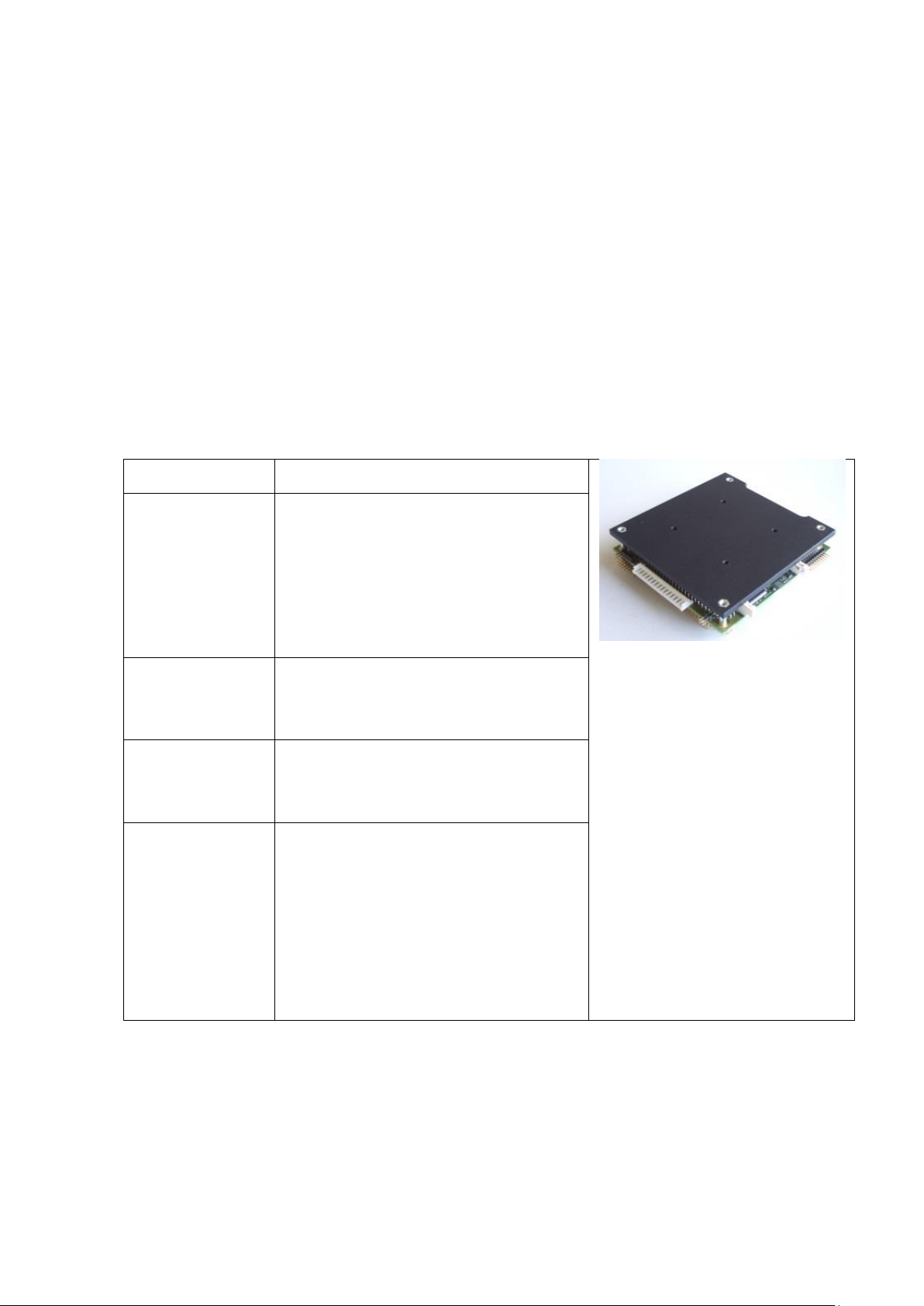
1.5 Heat sink solutions ..................................................................................................................... 9
Heat spreader: ............................................................................................................................................................ 9
Passive heat sink: ................................................................................................................................................... 10
Active heat sink: ...................................................................................................................................................... 10
2 Getting Started 12
2.1 Connector and Jumper Locations .......................................................................................... 12
Bottom ......................................................................................................................................................................... 12
Top ................................................................................................................................................................................ 13
13
2.2 LED indicators............................................................................................................................ 14
TME-104P-CMx-GF-1V7 Rev 1.7 i
Page 4

2.3 Hardware Setup ........................................................................................................................ 15
3 Module Description 16
3.1 Processor .................................................................................................................................... 16
3.2 Chipset ........................................................................................................................................ 17
3.3 Graphics-Controller .................................................................................................................. 21
VGA Connector (X15) ........................................................................................................................................... 23
LVDS Configuration ............................................................................................................................................... 24
LVDS Connector (X13) ......................................................................................................................................... 24
LVDS Color Mapping ............................................................................................................................................ 25
Backlight Connector (X5) .................................................................................................................................... 25
Display Voltage Jumpers (X22) ........................................................................................................................ 26
3.4 Ethernet Controller ................................................................................................................... 26
Ethernet Connector (X10) ................................................................................................................................... 27
3.5 On-Board Power Supply .......................................................................................................... 27
Power Connector (X21) ....................................................................................................................................... 27
Real Time Clock Backup (BAT1) ...................................................................................................................... 28
3.6 SATA ............................................................................................................................................ 28
SATA Connector (X27) ......................................................................................................................................... 29
CFast Connector (X27) ......................................................................................................................................... 29
3.7 PS/2 Interface ............................................................................................................................ 30
Keyboard and Mouse Connector (X20) ....................................................................................................... 30
External Battery ....................................................................................................................................................... 30
Power Button ........................................................................................................................................................... 30
Reset Button ............................................................................................................................................................. 31
Speaker ....................................................................................................................................................................... 31
3.8 Load BIOS defaults ................................................................................................................... 32
Jumper Load BIOS defaults (X23) ................................................................................................................... 32
TME-104P-CMx-GF-1V7 Rev 1.7 ii
Page 5

BIOS-DISABLE ........................................................................................................................................................... 32
Watchdog Timer ..................................................................................................................................................... 32
HDD LED..................................................................................................................................................................... 33
3.9 USB 2.0 Ports ............................................................................................................................. 33
USB 2.0 Connectors (X6, X7, X8) ..................................................................................................................... 33
3.10 HD Audio.................................................................................................................................... 34
Audio Connector (X1)........................................................................................................................................... 35
GPIO and FAN (X2)................................................................................................................................................ 35
3.11 BIOS Programming................................................................................................................... 36
BIOS Recovery Connector (X9) ........................................................................................................................ 36
3.12 Serial Ports ................................................................................................................................. 37
COM Connector (X24) .......................................................................................................................................... 38
RS485-Termination ................................................................................................................................................ 39
3.13 CPU Fan Supply ......................................................................................................................... 39
CPU Fan Connector (X18)................................................................................................................................... 39
3.14 SEMA functions ......................................................................................................................... 40
Board Specific SEMA functions ........................................................................................................................ 41
Voltages ...................................................................................................................................................................... 41
Main Current ............................................................................................................................................................ 41
Exception Codes ..................................................................................................................................................... 42
SMC Flags .................................................................................................................................................................. 43
SMC Status ................................................................................................................................................................ 43
3.15 PC/104-Plus Bus Interface ...................................................................................................... 44
PC/104 Bus Connector (X17) ............................................................................................................................ 44
3.16 PC/104 Bus Interface ............................................................................................................... 45
PC/104 Bus Connector (X14) ............................................................................................................................ 46
4 Using the Module 47
TME-104P-CMx-GF-1V7 Rev 1.7 iii
Page 6

4.1 BIOS ............................................................................................................................................. 47
Configuring the Phoenix BIOS ......................................................................................................................... 47
Initialize BIOS at first startup ............................................................................................................................ 47
Booting from alternative device ...................................................................................................................... 47
EFI Shell....................................................................................................................................................................... 47
Jumper BIOS Defaults .......................................................................................................................................... 47
4.2 Drivers ......................................................................................................................................... 75
4.3 Live-LED Programming ............................................................................................................ 75
4.4 Watchdog Programming ......................................................................................................... 75
4.5 GPIO programming .................................................................................................................. 76
4.6 Reading Temperatures ............................................................................................................ 76
4.7 Reading Voltages ...................................................................................................................... 76
4.8 Memory Address Map ............................................................................................................. 78
4.9 I/O Address Map ...................................................................................................................... 79
4.10 Interrupts ................................................................................................................................... 80
4.11 DMA Channels ........................................................................................................................... 81
Appendix A, Contact Information A
Appendix B, Additional Information B
Appendix C, Getting Help C
Appendix D, Revision History D
TME-104P-CMx-GF-1V7 Rev 1.7 iv
Page 7

Acronyms
ACPI Advanced Configuration and Power Management Interface
AES Advanced Encryption Standard
APM Advanced Power Management
APU Accelerated Processing Unit
ATA Advanced Technology Attachment
BIOS Basic Input Output System
BPP Bits Per Pixel
CD Compact Disc
COM Communication Equipment
CRT Cathode Ray Tube
CM CoreModule
DAC Digital-to-Analog-Converter
DDR Double Data Rate
DMA Direct Memory Access
DOT Dynamic Overclocking Technology
EIDE Enhanced Integrated Device Electronics
EMC Electromagnetic Compatibility
ETH Ethernet
FIFO First In First Out
FPU Floating Point Unit
FWH Firmware Hub
GPIO General Purpose Input Output
HDD Hard Disk Drive
I²C Inter-Integrated Circuit
IP Internet Protocol
ISA Industry Standard Architecture
LCD Liquid Crystal Display
LED Light Emitting Diode
LPC Low Pin Count
LVDS Low Voltage Differential Signaling
MAC Media Access Control
MMU Memory Management Unit
PCI Peripheral Component Interconnect
PHY Physical Interface
PLL Phase-Locked Loop
PS/2 Personal System/2
PWR Power
SEMA Smart Embedded Management Agent
SMB System Management Bus
SMC System Management Controller
SPI Serial Peripheral Interface
SSD Solid State Drive
SVGA Super Video Graphics Array
TME-104P-CMx-GF-1V7 Rev 1.7 v
Page 8

TCP Transmission Control Protocol
TLB Translation Look-aside Buffer
UART Universal Asynchronous Receiver Transmitter
USB Universal Serial Bus
UDMA Ultra-Direct Memory Access
UDP User Datagram Protocol
VGA Video Graphics Array
WDOG Watchdog
TME-104P-CMx-GF-1V7 Rev 1.7 vi
Page 9

1 Overview
APU
AMD G-Series T56N
o 1.65GHz Dual Core
o Max. TDP 18W
o AMD Radeon™ HD 6320
o 64KB L1 / 2x512KB L2 cache
o DDR3 SDRAM up to 1333 MT/s (667MHz)
AMD G-Series T40R
o 1.0GHz Single Core
o Max. TDP 5.5W
o AMD Radeon™ HD 6250
o 64KB L1 / 1x512KB L2 cache
o DDR3 SDRAM up to 1066 MT/s (533MHz)
AMD G-Series T16R
o 615 MHz Single Core
o Max. TDP 4.5W
o AMD Radeon™ HD 6250
o 64KB L1 / 1x512KB L2 cache
o DDR3 SDRAM up to 1066 MT/s (533MHz)
AMD Virtualization™ Technology
Main Memory
DDR3 SODIMM up to 4GB
1.1 Introduction
The standard-sized PC/104 Plus board is intended for applications in areas like medical, digital signage,
transport, and traffic control. It features an advanced graphics controller with Direct-X11 support. Versions with
dual core or single core processor are available. The CoreModule®x-GF runs Windows and Linux.
The accelerated processing unit (APU) supports single or dual independent high resolution displays and
exceptional multi-media capability with hardware decode support for H.264, VC-1, MPEG2, WMV, DivX and
Adobe Flash. DirectX® 11 support guarantees awesome graphics performance, stunning 3D visual effects and
dynamic interactivity. Advanced discrete-level GPU with OpenGL 4.0 and OpenCL™ 1.1 support in an integrated
device provides support to build the designs of tomorrow, today. Unprecedented graphics performance per
watt through advanced graphics and hardware acceleration delivers over 3X performance per watt of previous
generation.
Features
TME-104P-CMx-GF-1V7 Rev 1.7 1 (81)
Page 10

Fusion Controller Hub
AMD A55E
Extension slots
1 x 32-bit PC/104-Plus
1 x 16-bit PC/104 with full DMA capability
Interfaces
Ethernet 1000BaseTx
1x SATA 6Gbps
CFAST
PS/2 Keyboard/Mouse
6 x USB 2.0 ports
2 x RS232/RS485, software selectable
5.1 channel audio (analog & SPDIF)
VGA
18/24 Bit LVDS for displays
MISC signals: external power button, I²C bus,
speaker, external reset button, external
battery connector
Power supply
Other configurations are possible. Please contact your local ADLINK Technology GmbH
representative to discuss requirements.
TME-104P-CMx-GF-1V7 Rev 1.7 2 (81)
Page 11
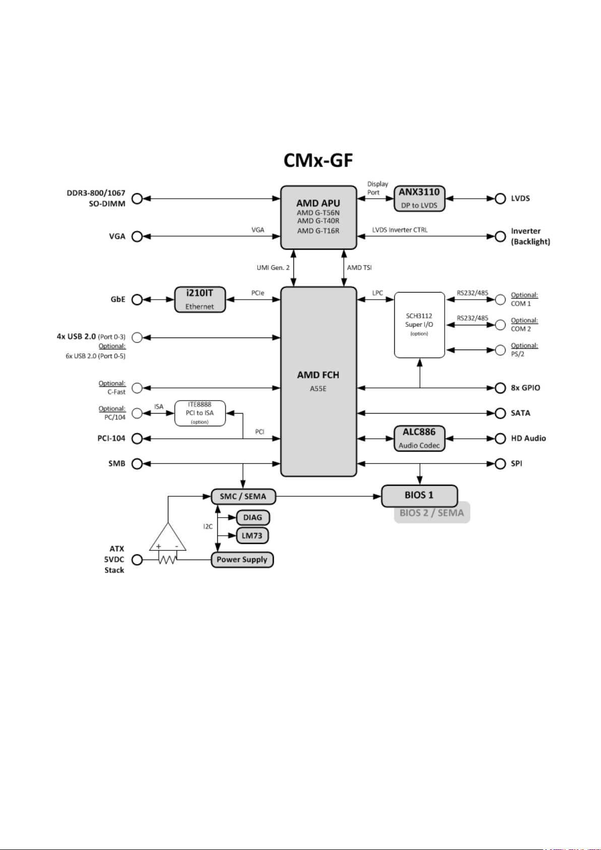
Block Diagram
TME-104P-CMx-GF-1V7 Rev 1.7 3 (81)
Page 12

1.2 Ordering Information
Order number
Description
703-0028-10
CM2-GF PC/104-Plus CPU board with AMD G-series T56N processor (Dual Core
1.65GHz/DDR3-1333) incl. heat spreader.
Operating temp. range: 0°C … +60°C
703-0029-10
CM2-GF PC/104-Plus CPU board with AMD G-series T40R processor (Single Core
1.0GHz/DDR3-1066) incl. heat spreader.
Operating temp. range: 0°C … +60°C
704-0007-10
CM3-GF PCI-104 CPU board with AMD G-series T16R processor (Single Core
615MHz/DDR3-1066) incl. heat spreader.
Operating temp. range: 0°C … +60°C
803-0028-10
CM2-GF PC/104-Plus CPU board with AMD G-series T56N processor (Dual Core
1.65GHz/DDR3-1333) incl. heat spreader.
Operating temp. range: -20°C … +70°C
803-0029-10
CM2-GF PC/104-Plus CPU board with AMD G-series T40R processor (Single Core
1.0GHz/DDR3-1066) incl. heat spreader.
Operating temp. range: -20°C … +70°C
804-0007-10
CM3-GF PCI-104 CPU board with AMD G-series T16R processor (Single Core
615MHz/DDR3-1066) incl. heat spreader.
Operating temp. range: -20°C … +70°C
903-0029-10
CM2-GF PC/104-Plus CPU board with AMD G-series T40R processor (Single Core
1.0GHz/DDR3-1066) incl. heat spreader.
Operating temp. range: -40°C … +85°C
904-0007-10
CM3-GF PCI-104 CPU board with AMD G-series T16R processor (Single Core
615MHz/DDR3-1066) incl. heat spreader.
Operating temp. range: -40°C … +85°C
CMx-GF Models
TME-104P-CMx-GF-1V7 Rev 1.7 4 (81)
Page 13
Cable Sets and Accessories
Order number
Description
763-0022-10
CM2-GF Adapter Cable Set
Power, GBit-Ethernet, VGA-CRT, 3x USB, COM1/2, 1x SATA, HD-Audio, PS/2
763-0022-11
CM3-GF Adapter Cable Set
Power, GBit-Ethernet, VGA-CRT, 3x USB, 1x SATA, HD-Audio
765-0049-11
Heat Sink passive for x03-0029-10 and x04-0007-10
765-0049-12
Heat Sink active for 703-0028-10 and 803-0028-10
760-0029-10
2GB PC3-8500 SODIMM in commercial temperature grade (0°C … +70°C)
760-0030-10
4GB PC3-8500 SODIMM in commercial temperature grade (0°C … +70°C)
960-0029-10
2GB PC3-8500 SODIMM in extended temperature grade (-40°C … +85°C)
960-0030-10
4GB PC3-8500 SODIMM in extended temperature grade (-40°C … +85°C)
Model Number
x03-0028-10
x03-0029-10
x04-0007-10
Form factor
PC/104-Plus
PC/104-Plus
PCI-104
PCI Bus (PCI-104)
1x
1x
1x
ISA Bus (PC/104)
1x
1x
-
CPU
T56N
T40R
T16R
CPU speed
1.65 GHz
1.0 GHz
615 MHz
CPU cores 2 1
1
VGA
1x
1x
1x
LVDS
1x
1x
1x
SATA 6 GB/s
1x
1x
1x
C-Fast slot
1x
1x
-
GbE
1x
1x
1x
COM
2x
2x
-
PS/2
1x
1x
-
GPIO
8x
8x
8x
HD Audio
1x
1x
1x
USB 2.0
6x
6x
4x
The following options are available for the CMx-GF.
CMx-GF Standard Variant Comparison Table
TME-104P-CMx-GF-1V7 Rev 1.7 5 (81)
Page 14

1.3
Supply voltage
+5 V DC
+5 V standby (only needed for suspend mode)
+12 V (only needed for LVDS display and expansion slots)
Rise time
< 10 ms
Supply voltage tolerance
± 5%
Inrush current
3.0A
Supply current
max. 3.7A (Windows 7, 3DMark11 Demo Mode & AMD ThermNow 100%)
typical 0.8A (Windows 7 idle mode)
typical 0.1A (suspend to RAM mode)
Temperature range
0 … 60 °C (standard version)
-20 … 60 °C (industrial version)
-40 … 85 °C (extended version)
Temperature change
max. 10K / 30 minutes
Humidity (relative)
10 … 90 % (non-condensing)
Pressure
450 … 1100 hPa
Temperature range
-40 … 85 °C
Temperature change
max. 10K / 30 minutes
Humidity (relative)
5 … 95 % (non-condensing)
Pressure
450 … 1100 hPa
MTBF at 25°C
172,356 hours
Specifications
Electrical Specifications
Environmental Specifications
Operating:
Non-Operating/Storage/Transport:
Mean Time Between Failures
TME-104P-CMx-GF-1V7 Rev 1.7 6 (81)
Page 15
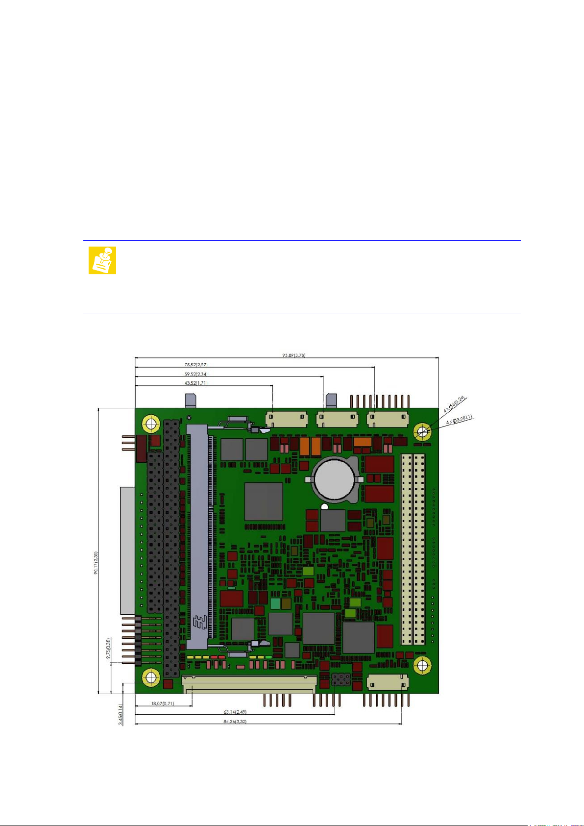
1.4 Mechanical
Dimensions (L x W)
90.2mm x 95.9mm
Height
Max. 14mm on top side above PCB (incl. heat spreader)
max. 9.3mm on bottom side above PCB (incl. memory module)
Weight
98 grams (incl. memory module)
Mounting
4 mounting holes
Note:
It is strongly recommended to use plastic spacers instead of metal spacers to
mount the board. With metal spacers, there is a possible danger to create a short
circuit with the components located around the mounting holes.
This can damage the board.
Bottom
TME-104P-CMx-GF-1V7 Rev 1.7 7 (81)
Page 16

Top
TME-104P-CMx-GF-1V7 Rev 1.7 8 (81)
Page 17
Part Number:
765-0048-10
Suitable for CPU /
Temperature Range:
CPU T16R 615MHz
CPU T40R 1GHz
CPU T56N 1.65 GHz
Standard temperature range 0°C to 60°C
Industrial temperature range -20°C to 70°C
Extended temperature range -40°C to 85°C
Suitable for CM2-GF
part numbers
703-0028-10 / 703-0029-10 / 704-0007-10
803-0028-10 / 803-0029-10 / 804-0007-10
903-0029-10 / 904-0007-10
Heat sink
Measurements
(L x W x H) / weight
measurements approx. 96 x 90 x 4 mm /
weight board and heat sink approx. 260 gr.
Remarks
On delivery the heat spreader is already
mounted on the board.
CMx-GF must be on top of the PC/104 stack.
Additional cooling by the customer is
necessary to fulfill requirements of the
commercial, industrial or extended
temperature range
1.5 Heat sink solutions
The following heat sink solutions are available for CMx-GF. The heat sink solutions have been tested under the
following conditions in climatic chamber:
Operating System: Windows 7
Application Software: AMD ThermNow! Thermal Analysis Tool / BurnIn Test Software
CPU load: full CPU load
Average airflow of the climate chamber: 0.5 m/s
Heat spreader
:
TME-104P-CMx-GF-1V7 Rev 1.7 9 (81)
Page 18
Passive heat sink
Part Number:
765-0049-11
Suitable for CPU /
Temperature Range:
CPU T16R 615MHz
CPU T40R 1GHz
Standard temperature range 0°C to 60°C
Industrial temperature range -20°C to 70°C
Extended temperature range -40°C to 85°C
Suitable for CM2-GF
part numbers
704-0007-10 / 804-0007-10 / 904-0007-10
703-0029-10 / 803-0029-10 / 903-0029-10
Heat sink
Measurements
(L x W x H) / weight
measurements approx. (with heat spreader)
96 x 90 x 34 mm / weight board, heat
spreader and heat sink approx. 460 gr.
Remarks
CMx-GF must be on top of the PC/104 stack.
The size of the heat sink
is designed to fulfill requirements of the
commercial, industrial and extended
temperature range without additional cooling.
Part Number:
765-0049-12
Suitable for CPU /
Temperature Range:
CPU T56N 1.65 GHz
Commercial temperature range 0°C to 60°C
Industrial temperature range -20°C to 70°C
Suitable for CM2-GF
part numbers
703-0028-10 / 803-0028-10
Heat sink
Measurements
(L x W x H) / weight
Measurements approx. (with heat spreader)
96 x 90 x 29 mm /
weight board, heat spreader and heat sink
approx. 465 gr.
Remarks
CMx-GF must be on top of the PC/104 stack.
The size of the heat sink
is designed to fulfill requirements of the
industrial temperature range without
additional cooling.
:
Active heat sink
:
TME-104P-CMx-GF-1V7 Rev 1.7 10 (81)
Page 19

Remarks:
Heat spreader is mounted with 10 mm spacers. Add 10 mm for the spacers to the measurements for
the total height above the PC/104 board.
All heat sinks are mounted by occupying the PC/104 mounting holes.
The CPU temperature may never exceed 100°C.
TME-104P-CMx-GF-1V7 Rev 1.7 11 (81)
Page 20
2 Getting Started
X6
USB0/1
X7
USB2/3
X8 (option)
USB4/5
X17
PCI-104
X13
LVDS
X5
Backlight
X22
Jumper
LVDS
and
Backlight
Power
Supply
X12
DDR3 SODIMM
BAT1
Battery
X2
GPIO / Fan
X14 (option)
PC/104
2.1 Connector and Jumper Locations
Bottom
The connector’s pin 1 is always marked with a golden triangle.
TME-104P-CMx-GF-1V7 Rev 1.7 12 (81)
Page 21
X24 (option)
COM
X16 (option)
CFast
X1
Audio
X10
LAN
X15
VGA
X27
SATA
X20 (option)
PS/2
RESET BUTTON
X21
Power
X18
CPU Fan
X23
Jumper
BIOS Defaults
SATA LED
X9
BIOS Service
X19
SMC Service
Top
TME-104P-CMx-GF-1V7 Rev 1.7 13 (81)
The connector’s pin 1 is always marked with a golden triangle.
Page 22
2.2 LED indicators
The onboard LED indicators provide a convenient way to check the board’s statuses. The boot success, power
status, IDE accesses, Watchdog and Ethernet accesses are all visible.
The LED indicators are located on bottom of the board, near the LVDS connector.
STATUS Yellow LED shows error codes in terms of failures.
PWR MODE Yellow LED is constantly lit if the boot process is complete and the board is running normally.
LED flashes when board goes in suspend to ram mode.
MAIN PSU Yellow LED lights up when Main Power is supplied.
WD Red LED lights up when Watchdog is triggered. Can only be reset by a power off sequence.
LIVE Red LED is on at startup while the board executes the BIOS power on self test (POST). After
that, it is freely usable by application programs. Chapter 4.3 shows a small sample program on
how to control it.
SATA Yellow LED flashes when SATA activity is recognized.
LINK Green LED shows the Ethernet Link status.
ACT Green LED flashes at Ethernet activity.
TME-104P-CMx-GF-1V7 Rev 1.7 14 (81)
Page 23
2.3 Hardware Setup
Caution Be sure to observe the EMC security measures. Make sure you are always at
the same potential as the module.
Caution Never connect or disconnect peripherals like HDDs or PCI and ISA boards
while the board's power supply is connected and switched on.
Note
The 5-amp value is the minimum you should have for the standard peripherals
mentioned. If you want to use additional peripherals, please plan your power
budget first. The system will not work without enough supply current for all your
devices.
Use the cable set provided by ADLINK Technology GmbH to connect the CMx-GF to a VGA monitor. Connect
either PS/2 or USB keyboard or mouse, respectively. Use the SATA cable to connect the hard disk. Make sure
that the pins match their counterparts correctly and are not twisted. If you plan to use additional peripherals,
now is the time to connect them, too.
Connect a 5-volt, 5-amp power supply to the power connector and switch the power on.
The display shows the BIOS messages. If you want to change the standard BIOS settings, press the <F2> key
to enter the BIOS menu. See chapter 4.1 for setup details.
If you need to load the BIOS default values, they can be automatically loaded at boot time. See chapter 3.8,
"Load Bios defaults", about loading BIOS defaults.
The CMx-GF boots from CD drives, USB floppies, USB sticks, hard disks, and CFast or Ethernet (PXE) devices.
Provided that any of these is connected and contains a valid operating system image, the display will show the
boot screen of your operating system.
The CMx-GF requires adequate cooling depending on the operating temperature range. Using the board
without cooling could damage the board permanently.
TME-104P-CMx-GF-1V7 Rev 1.7 15 (81)
Page 24

3 Module Description
3.1 Processor
The AMD Embedded G-Series processor is the world’s first integrated circuit to combine a low-power CPU and
a discrete-level GPU into a single embedded Accelerated Processing Unit (APU).This unprecedented level of
graphics integration builds a new foundation for high-performance, multi-media content delivery in a small
form factor and power efficient platform for a broad range of embedded designs. Based on a brand new,
power-optimized core, the AMD Embedded G-Series platform delivers new levels of performance in a compact
BGA package that is ideal for low power designs in embedded applications such as Digital Signage, x86 SetTop-Box (xSTB), IP-TV, Thin Client, Information Kiosk, Point-of-Sale, Casino Gaming, media servers, and
industrial control systems.
APU configurations are available with single or dual x86 cores and two levels of graphics and video
performance. Each APU supports single or dual-independent high resolution displays and exceptional multimedia capability with hardware decode support for H.264, VC-1, MPEG2, WMV, DivX and Adobe Flash.
DirectX® 11 support lets you enjoy awesome graphics performance, stunning 3D visual effects, and dynamic
interactivity. Advanced, discrete-level GPU with OpenGL 4.0 and OpenCL™ 1.1 support in an integrated device,
provides support to build the designs of tomorrow, today.
APU Features
High-speed device interconnect
High-performance integrated x86 core(s)
Integrated, cutting-edge graphics processor
High-bandwidth, low-latency integrated memory controller
Low-latency platform interface
x86 Core Architecture
Single or Dual x86 Processor
Advanced Branch Predictor
Out-of-Order Instruction Execution
Full OOO Instruction Execution
Full OOO Load/Store Engine
High-Performance Floating Point
AMD64, 64-bit ISA
SSE1,2,3, SSSE3 ISA, SSE4A
Secure Advanced Virtualization
Integrated DDR3 Memory Controller
Support for solder-down, SODIMM and DIMM memory, two slots, non-ECC type
64-bit DDR3 SDRAM controller operating at frequencies up to 1333 MT/s (667 Mhz)
TME-104P-CMx-GF-1V7 Rev 1.7 16 (81)
Page 25

Large High-Performance On-Chip Cache
32KB I-Cache, 32KB D-Cache
512KB L2 per Core
Integrated Display Interfaces
Dual, independent display support (n/a on CMx-GF)
Dual-link or dual single-link DVI (n/a on CMx-GF)
HDMI™ (n/a on CMx-GF)
Dual DisplayPort (n/a on CMx-GF)
LVDS
Analog VGA
AMD Virtualization™ Technology (AMD-V™)
SVM lock and unlock
Nested paging
Next RIP
LBR virtualization
8 address space identifiers
Performance counter guest/host bit
Nested page table fault info
3.2 Chipset
The AMD A55E (Hudson-E1) is AMD’s first generation Fusion Controller Hub (FCH) designed to deliver the
quality and performance needed for everyday computing, multitasking, and multimedia functionality.
Supporting AMD's Fusion Accelerated Processor Units (APUs), Hudson-E1 FCH replaces the traditional two-chip
approach with a new, single-chip architecture, reducing power consumption and improving system
performance while reducing the overall chipset footprint. The AMD Hudson-E1 FCH provides expanded I/O
connectivity for advanced usage models to take advantage of modern peripheral devices.
Unified Media Interface (UMI)
1-, 2-, or 4-lane Unified Media Interface connecting the FCH with the APU
Automatic detection of lane configuration on boot up
Dynamic lane width up/down configuration on detecting bandwidth requirement
Supports transfer rate of up to 5.0 GT/s per lane
Clock speed can be locked at 2.5 GHz for power saving
PCI Express® 2.0 Controller
4-lane PCI Express® (PCIe®) 2.0 interface, supporting up to four general purpose (GPP) devices (n/a
on CMx-GF).
PCI Host Bus Controller
Supports PCI bus at 33MHz
Supports PCI Rev. 2.3 specification
TME-104P-CMx-GF-1V7 Rev 1.7 17 (81)
Page 26

Supports up to four bus master devices
Supports 40-bit addressing
Interrupt steering supported for plug-n-play devices
Supports concurrent PCI operations
BIOS/hardware support to hide PCI device
Supports spread spectrum
USB Controllers
One OHCI and three EHCI host controllers to support 14 USB 2.0 ports (six on CM2-GF and four on
CM3-GF) and two dedicated USB 1.1 ports (n/a on CMx-GF)
Supports ACPI S1 ~ S5 (only supported on USB port 4 and 5)
Supports USB keyboard/mouse functionality for legacy Operating Systems
Supports individual port disable capability
DMA Controller
Two cascaded 8237 DMA controllers
Supports LPC DMA
Supports type F DMA
LPC host bus Controller
Supports LPC-based super I/O and flash devices
Supports two master/DMA devices
Supports TPM version 1.1/1.2 devices for enhanced security (n/a on CMx-GF)
Supports SPI devices
Supports a maximum SPI ROM size of 16MB
SATA Controller
Supports six Third generation SATA ports (backward compatible with Second and First generation
devices)
Complies with SATA 2.6 specification
Supports two modes of operation
o IDE emulation mode
o AHCI mode (compliant with AHCI specification revision 1.2)
RAID 0, RAID 1, RAID 5, RAID 10 support (n/a on CMx-GF)
NCQ support
Device or Host Initiated Power Management (DIPM /HIPM) support
Hot plug support
FIS-based switching support
e-SATA support (n/a on CMx-GF)
Zero Power ODD support
High Definition Audio
Four independent output streams (DMA)
Four independent input streams (DMA)
Multiple channels of audio output per stream
Supports up to four codecs (one on CMx-GF)
TME-104P-CMx-GF-1V7 Rev 1.7 18 (81)
Page 27

Up to 192kHz sample rate and 32-bit audio
64-bit addressing capability for DMA bus master and MSI
Unified Audio Architecture (UAA) compatible
HD Audio registers can be located anywhere in the 64-bit address space
Supports 3.3V/1.5V dual-voltage interface for power saving
Gigabit Ethernet Media Access Controller (GbE MAC)
(n/a on CMx-GF)
Timers
8254-compatible timer
Microsoft® High Precision Event Timer (HPET)
ACPI power management timer
Real Time Clock (RTC)
256-byte battery-backed CMOS RAM
Hardware supported century rollover
Hardware supported day-light saving feature
RTC battery monitoring feature
Power Management
ACPI specification 3.0 compliant power management schemes
Supports CPU C1e, C2, C3, C3 pop-up, C4, and C5 states
Supports system S0, S1, S3, S4, and S5 states
Wakeup events for S1, S3, S4, and S5 generated by:
o Any GEVENT pin (n/a on CMx-GF)
o Any GPM pin (n/a on CMx-GF)
o USB
o Power Button
o Internal RTC wakeup
o SMI event
o Consumer IR (n/a on CMx-GF)
CPU SMM support, generating SMI message upon power management events
CLKRUN# support for PCI power management (n/a on CMx-GF)
Provides clock generator and CPU STPCLK# control
Supports hardware monitoring and fan control (available on CMx-GF via SEMA)
ALPM (HIPM) on SATA
DIPM on SATA
Integrated Clock Function
Provides two auxiliary clocks, which can be configured to 25MHz, 14.318MHz, or 48MHz
Provides system clocks for APU
Provides clocks for UMI, PCIe graphics (integrated or external), and up to nine PCIe GPP ports
TME-104P-CMx-GF-1V7 Rev 1.7 19 (81)
Page 28
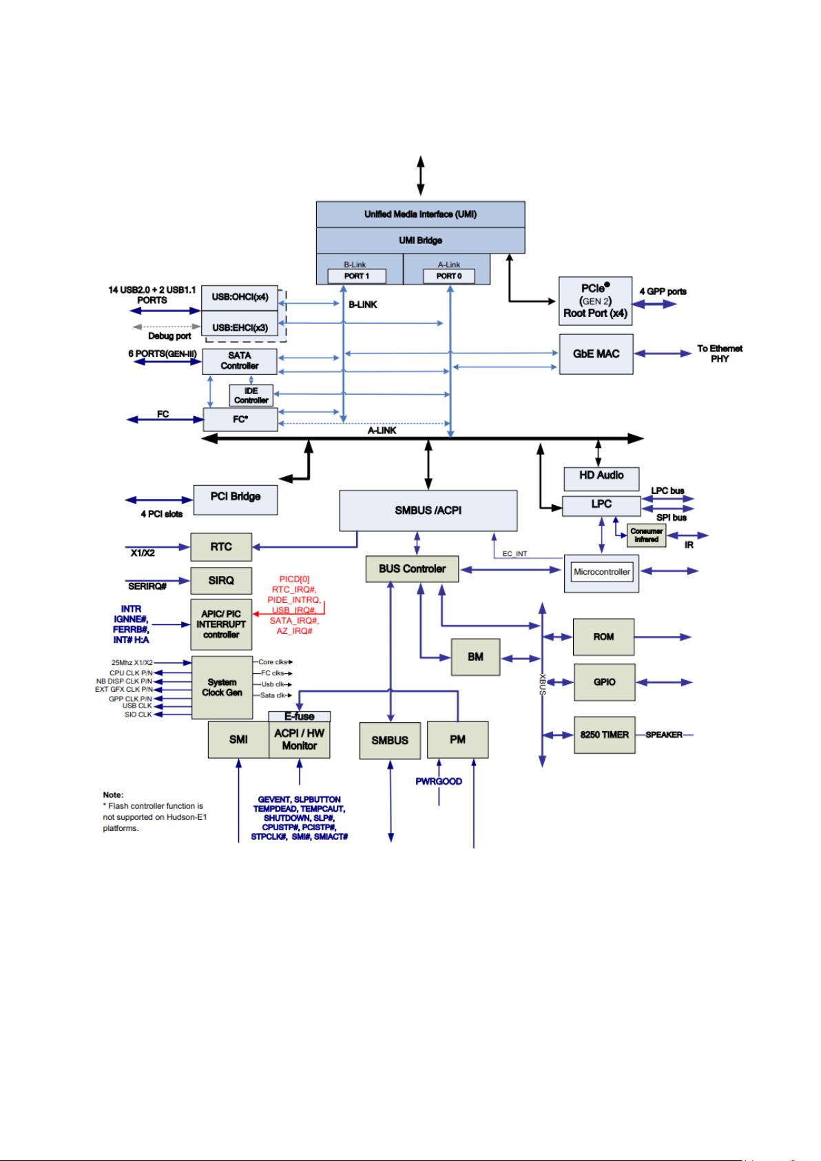
Hudson-E1 FCH Block Diagram
TME-104P-CMx-GF-1V7 Rev 1.7 20 (81)
Page 29

3.3 Graphics-Controller
This section lists the graphics features available for the AMD G-Series processor when the internal GPU is
enabled.
Power Management
Frame buffer compression
GPU power gating
UVD power gating
Graphics memory controller (GMC) power gating
AMD PowerPlay™ power management technology
Vari-Bright™ technology
Dynamic refresh rate
3D graphics engine power gating during video playback
AMD Dynamic Switchable Graphics (DSG) technology*
* AMD Dynamic Switchable Graphics technology is available with limited mobile discrete graphics processors
and on the Windows® 7 operating system.
2D Acceleration Features
Highly-optimized 128-bit engine, capable of processing multiple pixels per clock
Hardware acceleration of Bitblt, line drawing, polygon and rectangle fills, bit masking, monochrome
expansion, panning and scrolling, scissoring, and full ROP support (including ROP3)
Optimized handling of fonts and text using AMD proprietary techniques
Game acceleration including support for Microsoft® DirectDraw: Double Buffering, Virtual Sprites,
Transparent Blit, and Masked Blit
Acceleration in 1/8/15/16/32-bpp modes:
o Pseudocolor mode for 8 bpp
o ARGB1555 and RGB565 modes for 16 bpp
o ARGB8888 mode for 32 bpp
Setup of 2D polygons and lines
Support for GDI extensions:
o In Windows XP and Windows Vista®: Alpha BLT, Transparent BLT, and Gradient Fill
o In Windows 7: Alpha BLT, Transparent BLT, Color Fill BLT, Stretch BLT, and Clear Type BLT
Hardware cursor (up to 64 bpp × 64 bpp × 32 bpp), with alpha channel for direct support of Windows
XP, Windows Vista and Windows 7 alpha cursor
3D Acceleration Features
DirectX® 11 compliant, including full-speed, 32-bit floating point per component operations
o Shader Model 5 geometry and pixel support in a unified shader architecture:
Vertex, pixel, geometry, compute, domain, and hull shaders
Full-speed, 32-bit and 64-bit floating point processing per component
High dynamic range rendering with floating point blending, texture filtering and anti-
aliasing support
High-performance dynamic branching and flow control
TME-104P-CMx-GF-1V7 Rev 1.7 21 (81)
Page 30

Shader instruction store, using an advance caching system
Advanced shader design, with ultra-threading sequencer for high-efficiency
operations
Advanced, high-performance branching support, including static and dynamic
branching
16-bit and 32-bit floating point components for high dynamic range computations
Full anti-aliasing on render surfaces up to and including 128-bit floating point
formats
Support for OpenCL™ 1.1
Support for OpenGL 3.2 and 2.1
Anti-Aliasing Filtering:*
o * Support for anti-aliasing filtering is dependent on application
o 2x/4x/8x modes
o Sparse multi-sample algorithm with gamma correction, programmable sample patterns, and
centroid sampling
o Temporal anti-aliasing
o Custom filter anti-aliasing with up to 12 samples per pixel
o Adaptive anti-aliasing mode
o Lossless color compression (up to 8:1) at all resolutions, up to and including widescreen
HDTV
Anisotropic Filtering:*
o * Support for anisotropic filtering is dependent on application
o 2x/4x/8x/16x modes
o Up to 128-tap texture filtering
o Anisotropic biasing to allow trading quality for performance
o Improved quality mode due to improved sub-pixel precision, and higher precision LOD
computations
o Advanced texture compression (3Dc+)
o High quality 4:1 compression for normal maps and luminance maps
o Angle-invariant algorithm for improved quality
o Works with single-channel or two-channel data format
HW support to overcome "Small batch" issues in CPU limited applications
3D resources virtualized to a 32-bit addressing space, for support of large numbers of render targets
and textures
Support for up to 16k x 16k textures, including 128-bit/pixel textures
Software-upgradeable, programmable arbitration logic maximizing memory efficiency
Fully associative texture, color, and Z cache design
Hierarchical Z and stencil buffers with early Z Test
Lossless Z-buffer compression for both Z and stencil
Fast Z-buffer clear
Fast color-buffer clear
Z cache optimized for real-time shadow rendering
Z and color compression resources virtualized to a 32-bit addressing space, for simultaneous support
of multiple render targets and textures
TME-104P-CMx-GF-1V7 Rev 1.7 22 (81)
Page 31

Motion Video Acceleration Features
Pin
Signal
Pin
Signal
1
Red
2
GND
3
Green
4
KEY
5
Blue
6
VGA_DDC_CLK
7
HSYNC
8
VGA_DDC_DATA
9
VSYNC
10
GND
Supports Adobe® Flash Player 10
UVD acceleration for MPEG4 Part 2 playback in Windows Media Player
Supports DVD, Blu-ray*, and SDTV/HDTV content playback with low CPU usage (only available on
T56N variants)
Motion video decode acceleration technology:
o Dedicated hardware (UVD 3) for H.264, MPEG4 Part 2, VC-1, and MPEG2 decode:
H.264 implementation based on the ISO/IEC 14496-10 specification
MPEG4 Part 2 implementation based on the ISO/IEC 14496-2 specification
VC-1 implementation based on the SMPTE 421M specification
MPEG2 implementation based on the IOS 13811-2 specification
o Microsoft DirectX video acceleration (DXVA) API (application programming interface) for
Windows operating system
Motion video process acceleration:
o Video scaling and YCrCb to RGB color space conversion for video playback and fully
adjustable color controls
o Motion adaptive and vector based de-interlacing filter eliminates video artifacts caused by
displaying interlaced video on non-interlaced displays, and by analyzing image and using
optimal de-interlacing functions on a per-pixel basis
o HD HQV and SD HQV support: noise removal, detail enchantment, color enhancement,
cadence detection, sharpness, and advanced de-interlacing
o Super up-conversion for SD to HD resolutions
o AMD SteadyVideo technology
o Multi-plane compositing engine for Blu-ray player applications (only available on T56N
variants)
VGA Connector (X15)
Connector type IDC 10-pin header, 2.00 mm
Adapter cable Article number 862-0019-10
TME-104P-CMx-GF-1V7 Rev 1.7 23 (81)
Page 32

Pin
Signal
Pin
Signal
1
VCC_LCD
2
VCC_LCD
3
GND
4
GND
5
LVDS_L3n
6
LVDS_L3p
7
LVDS_LCLKn
8
LVDS_LCLKp
9
GND
10
LVDS_L2n
11
LVDS_L2p
12
LVDS_L1n
13
LVDS_L1p
14
LVDS_L0n
15
LVDS_L0p
16
GND
17
LVDS_U3n
18
LVDS_U3p
19
LVDS_UCLKn
20
LVDS_UCLKp
21
GND
22
LVDS_U2n
23
LVDS_U2p
24
LVDS_U1n
25
LVDS_U1p
26
LVDS_U0n
27
LVDS_U0p
28
GND
29
LVDS_DDC_CLK
30
LVDS_DDC_DATA
Caution
The maximum current on all supply pins is 1A.
LVDS Configuration
To ease usage of these displays it is possible to select the display and backlight supply voltages with the
onboard voltage selector jumpers (LVDS and Backlight.) See below.
LVDS Connector (X13)
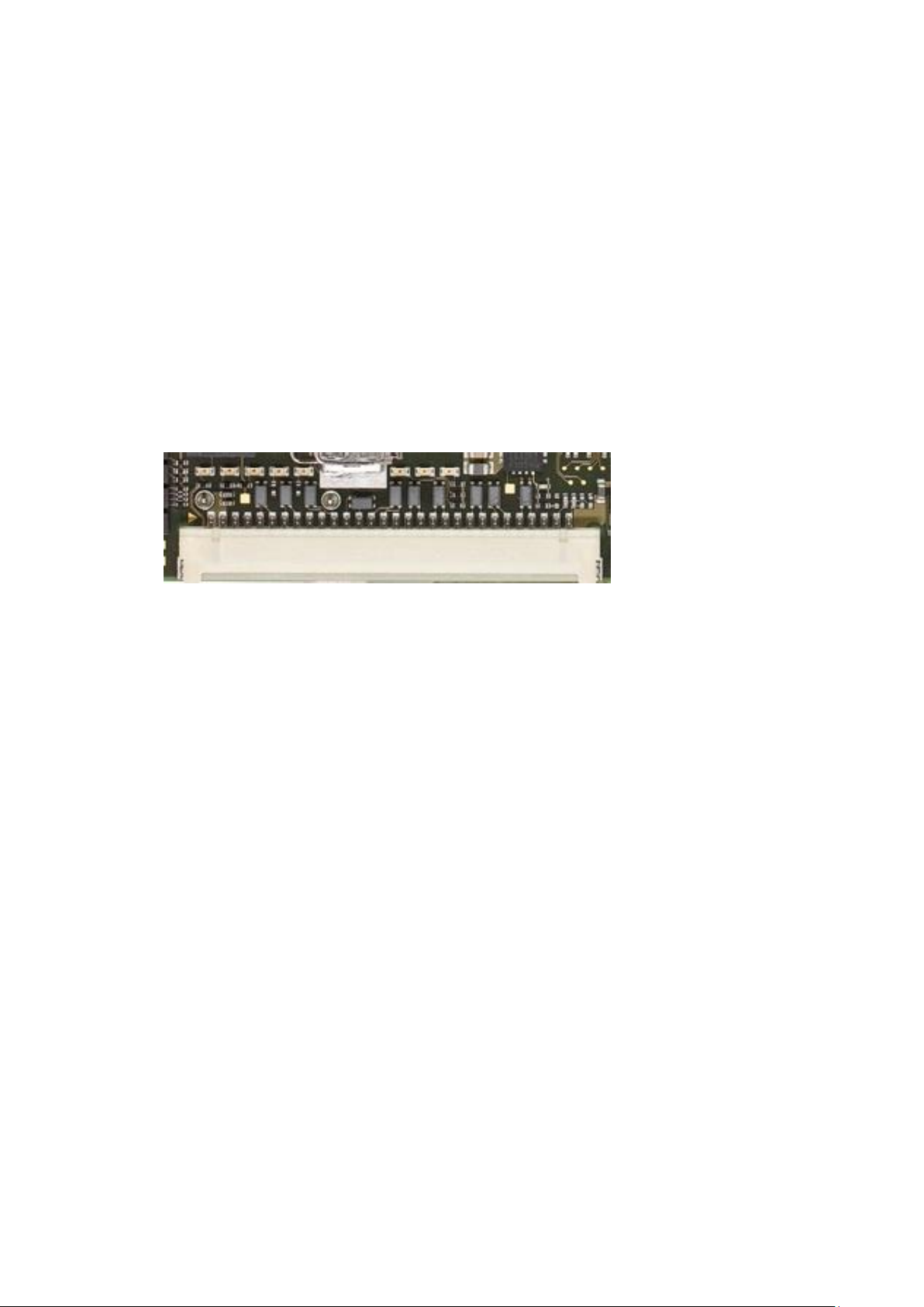
Connector type Hirose DF14 30-pin header
Adapter cable n/a
TME-104P-CMx-GF-1V7 Rev 1.7 24 (81)
Page 33

LVDS Color Mapping
Pin
Signal
1
+12V
2
+12V
3
+5V
4
+5V
5
EN
6
VCC*
7
GND
8
GND
Caution
The maximum current on all supply pins is 1A.
1 2 3 4 5 6 7 CLKL 1 1 0 0 0 1 1 L0
Green2
Red7
R6
R5
R4
R3
R2
L1
Blue3
B2
G7
G6
G5
G4
G3
L2
DE
VS
HS
B7
B6
B5
B4
L3
0/B1
B1
B0
G1
G0
R1
R0
CLKU 1 1 0 0 0 1 1 U0
G2
R7
R6
R5
R4
R3
R2
U1
B3
B2
G7
G6
G5
G4
G3
U2
DE
VS
HS
B7
B6
B5
B4
U3
0/B1
B1
B0
G1
G0
R1
R0
Backlight Connector (X5)
Connector type Hirose DF13, 8-pin
Adapter cable n/a
*That voltage can be selected using the jumper "Backlight", shown on next table.
TME-104P-CMx-GF-1V7 Rev 1.7 25 (81)
Page 34

Display Voltage Jumpers (X22)
Pin
Signal (Backlight)
Pin
Signal (LVDS)
1
+12V
2
+3.3V
3
Backlight Voltage
4
Display Voltage
5
+5V
6
+5V
default jumper setting
Jumper
Connector type: IDC 6-pin header, 2.00 mm
Use a 2 mm jumper between 1-3 or 3-5 to select the backlight voltage.
Use a 2 mm jumper between 2-4 or 4-6 to select the display voltage.
LVDS and Backlight Power Supply
3.4 Ethernet Controller
The Intel i210 Ethernet controller supports 10/100/1000-Mbit speeds.
Features
IEEE 802.3 compliant
Auto Negotiation
Audio-video bridging
• IEEE 1588/802.1AS precision time synchronization
• IEEE 802.3Qav traffic shaper (with software extensions)
Jumbo Frame Support
Interrupt moderation, VLAN support, IP checksum offload
Four transmit and four receive queues
Advanced cable diagnostics, auto MDI-X
ECC – error correcting memory in packet buffers
IEEE 802.3az Energy Efficient Ethernet (EEE)
TME-104P-CMx-GF-1V7 Rev 1.7 26 (81)
Page 35

Ethernet Connector (X10)
Pin
Signal
Pin
Signal
1
ETH_MX0n
2
ETH_MX0p
3
ETH_MX1n
4
ETH_MX1p
5
NC
6
KEY
7
ETH_MX2n
8
ETH_MX2p
9
ETH_MX3n
10
ETH_MX3p
Note
This 3.3V must not be used to supply external electronic devices with high-power
consumption like other PC/104 boards or displays.
Pin
Signal (standard)
Signal (5V only)
1
+5V
+5V
2
GND
GND
3
+5V
+5V
4
GND
GND
5
+5V
+5V
6
+5V Standby
NC 7 GND
GND
8
PSON#
GND
Connector type IDC 10-pin header, 2.00 mm
Adapter cable Article number 862-0018-10
3.5 On-Board Power Supply
The on-board power supply generates all necessary voltages from the single supply voltage of 5 volts. The
generated 3.3 volts are available on the connectors "Flat Panel" and "LVDS".
Power Connector (X21)
Connector type JST B15B-EH-A, 15-pin
Adapter cable Article number 862-0044-10
TME-104P-CMx-GF-1V7 Rev 1.7 27 (81)
Page 36

9
PWROK
NC
10
+3.3V
NC
11
GND
GND
12
+12V (only for PC104
slot
and backlight power
supply)
NC
13
+12V (only for PC104
slot
and backlight power
supply)
NC
14
GND
GND
15
-12V (only for PC104
slot)
NC
Note The default cable adapter supports the connection of 12V power supply.
If the 5V only power supply is required leave these pins open.
The board can also be supplied over PC/104- or PC/104 plus bus.
Real Time Clock Backup (BAT1)
A battery is integrated on board. This battery is necessary to power the real-time clock (RTC) if the power
supply is switched off.
Battery Type: CR1225, 3-Volt
3.6 SATA
The integrated Serial ATA controller processes host commands and transfers data between the host and Serial
ATA devices. It supports six independent Serial ATA channels. Each channel has its own Serial ATA bus and
supports one Serial ATA device. With respect to the transfer rate, the integrated SATA controller supports First
Generation (1.5 Gbit/s), Second Generation (3.0 Gbit/s), and Third Generation (6.0 Gbit/s) SATA ports. On CMxGF there is one SATA connector and one CFast connector available.
The SATA controller can operate in three modes:
SATA and CFast are configured as SATA AHCI mode.
SATA and CFast are configured as IDE mode. In this configuration, the SATA controller is configured
into two IDE controllers, with the programming interface of channels 0 to 3 (SATA) under the first IDE
controller and that of channels 4 and 5 (CFast) under the second IDE controller.
TME-104P-CMx-GF-1V7 Rev 1.7 28 (81)
Page 37

SATA is configured as SATA AHCI, and CFast is configured as IDE mode. In this configuration, the
Pin
Signal
1
GND
2
Data_TX+
3
Data_TX-
4
GND
5
Data_RX-
6
Data_RX+
7
GND
Pin
Signal
Pin
Signal
1
GND
13
NC
2
Data_TX+
14
GND
3
Data_TX-
15
SATA_ACT#
4
GND
16
NC
5
Data_RX-
17
NC
6
Data_RX+
18
NC 7 GND
19
NC 8 NC
20
+3.3V
9
GND
21
+3.3V
10
NC
22
GND
11
NC
23
GND
12
NC
24
NC
programming interfaces of channels 4 and 5 (CFast) are under the IDE controller.
SATA Connector (X27)
Connector type: SATA
Adapter cable n/a
CFast Connector (X27)
Connector type: CFast
TME-104P-CMx-GF-1V7 Rev 1.7 29 (81)
Page 38

3.7 PS/2 Interface
Pin
Signal
Pin
Signal
1
Speaker
2
Mouse Clock
3
Reset-In
4
Mouse Data
5
KB Data
6
KB Clock
7
GND
8
+5V Standby
9
Ext. Battery
10
Power Button
Pin
Signal
Pin
Signal
1
Speaker
2
Mouse Clock
3
Reset-In
4
Mouse Data
5
KB Data
6
KB Clock
7
GND
8
+5V Standby
9
Ext. Battery
10
Power Button
PS/2-connectors for mouse and keyboard are shared with several system signals.
An adapter cable for the PS/2 devices is available.
Keyboard and Mouse Connector (X20)
Connector type IDC 10-pin header, 2.00 mm
Adapter cable Article number 862-0022-10
External Battery
A connected external battery should replace or support the mounted one to keep accurate date and time. It is
recommended to use a model with 3 Volts (CR1225). The time and date will be lost if the power falls to 2.5
Volts.
For real-time calculation (worst case), 4 µA (25°C) are needed when the board is not running. That value can
rise depending on the connected cables and higher temperatures.
Power Button
To power up/down the board, the signal Power Button must be pulled to GND.
TME-104P-CMx-GF-1V7 Rev 1.7 30 (81)
Page 39

Pin
Signal
Pin
Signal
1
Speaker
2
Mouse Clock
3
Reset-In
4
Mouse Data
5
KB Data
6
KB Clock
7
GND
8
+5V Standby
9
Ext. Battery
10
Power Button
Pin
Signal
Pin
Signal
1
Speaker
2
Mouse Clock
3
Reset-In
4
Mouse Data
5
KB Data
6
KB Clock
7
GND
8
+5V Standby
9
Ext. Battery
10
Power Button
Pin
Signal
Pin
Signal
1
Speaker
2
Mouse Clock
3
Reset-In
4
Mouse Data
5
KB Data
6
KB Clock
7
GND
8
+5V Standby
9
Ext. Battery
10
Power Button
Reset Button
To reset the board, the signal Reset Button must be pulled to GND.
Speaker
The speaker signal is located on the PS/2, IDC10 Header. A standard PC Speaker can be connected between
the signals Speaker and +5V Standby.
TME-104P-CMx-GF-1V7 Rev 1.7 31 (81)
Page 40

Pin
Signal
Pin
Signal
1
SATA_ACT#
2
BIOS_DISABLE#
3
WD_ACTIVE
4
GND
5
LAN_ACTIVITY_LED#
6
BIOS_DEFAULTS#
Pin
Signal
Pin
Signal
1
SATA_ACT#
2
BIOS_DISABLE#
3
WD_ACTIVE
4
GND
5
LAN_ACTIVITY_LED#
6
BIOS_DEFAULTS#
3.8 Load BIOS defaults
In rare cases, the system may not start because of certain BIOS settings. If that is the case, it is highly
recommended to first restore the BIOS factory settings before any debugging is done. This is achieved with
Load Optimized Defaults in the main setup menu. If you cannot reach the BIOS setup because of bad system
configuration, use the jumper near the power connector:
Power off the board
Set the 2.00 mm jumper Load BIOS defaults between pins 4 and 6
Power on the board
Jumper Load BIOS defaults (X23)
BIOS-DISABLE
In rare cases, the system may not start because of certain BIOS settings or because of failed BIOS update.
Choose BIOS_DISABLE# to select the second BIOS (recovery).
Power off the board
Set the 2.00 mm jumper Load BIOS defaults between pins 2 and 4
Power on the board
The system now uses the recovery BIOS
Watchdog Timer
TME-104P-CMx-GF-1V7 Rev 1.7 32 (81)
Page 41

A Watchdog Timer is integrated on board and managed with the SMC SEMA functionality. There are multiple
Pin
Signal
Pin
Signal
1
SATA_ACT#
2
BIOS_DISABLE#
3
WD_ACTIVE
4
GND
5
LAN_ACTIVITY_LED#
6
BIOS_DEFAULTS#
Pin
Signal
Pin
Signal
1
SATA_ACT#
2
BIOS_DISABLE#
3
WD_ACTIVE
4
GND
5
LAN_ACTIVITY_LED#
6
BIOS_DEFAULTS#
Note: Not all USB keyboard models are supported.
ways of activating the Watchdog Timer. Refer to chapter 3.14 for more details on the SMC.
HDD LED
SATA_ACT# provides the LED interface for SATA devices or CFast. The signal is active low and can sync an LED
that is connected to 3.3V.
3.9 USB 2.0 Ports
The Hudson-E1 contains three Enhanced Host Controller Interface (EHCI) host controllers, which support up to
fourteen USB 2.0 high-speed root ports. USB 2.0 allows data transfers up to 480Mb/s using the same pins as
the fourteen USB full-speed/low-speed ports. The Hudson-E1 contains port-routing logic that determines
whether a USB port is controlled by one of the UHCI controllers or by one of the EHCI controllers.
The CMx-GF uses six of the fourteen ports. They are available for the application on three USB connectors,
each providing two ports using a different EHCI controller for full USB performance. A standard adapter cable
is available, too.
A USB keyboard will function under MSDOS without special driver software.
Ports 0/1 are powered in S3 to support wakeup from keyboard and mouse.
USB 2.0 Connectors (X6, X7, X8)
Connector type Hirose DF13 8-pin
Adapter cable Article number 862-0058-10
TME-104P-CMx-GF-1V7 Rev 1.7 33 (81)
Page 42

PIN
Signal
1
VCC_USB0/2/4
2
USB0/2/4-
3
USB0/2/4+
4
GND_USB0/2/4
5
GND_USB1/3/5
6
USB1/3/5-
7
USB1/3/5+
8
VCC_USB1/3/5
3.10 HD Audio
The High Definition (HD) Audio Controller communicates with the external HD Audio codec(s) over the HD
Audio Link. The Hudson-E1 HD Audio Controller consists of four independent output DMA engines and four
independent input DMA engines that are used to move data between system memory and the external
codec(s). The controller can support up to four audio or modem codecs in any combination.
The CMx-GF uses a codec from Realtek. The ALC888 is a high-performance 7.1+2 Channel High Definition
Audio Codec.
The following audio I/Os are used by the CMx-GF:
Analog Input (All ADC support 44,1k/48k/96kHz sampling rate)
o Microphone left and right
o Line In left and right
Analog output (All DAC support 44,1k/48k/96/192kHz sampling rate)
o Front left and right
o Rear left and right
o Center and Subwoofer
Digital input (16/20/24-bit S/PDIF-in support 44,1k/48k/96/192kHz sampling rate)
o S/PDIF
Digital output (16/20/24-bit S/PDIF-out support 44,1k/48k/96/192kHz sampling rate)
o S/PDIF
TME-104P-CMx-GF-1V7 Rev 1.7 34 (81)
Page 43

Audio Connector (X1)
Pin
Signal
Pin
Signal
1
LineOut_R
2
LineOut_L
3
Surround_R
4
Surround_L
5
LFE
6
Center
7
GND_Audio
8
GND_Audio
9
LineIn_R
10
LineIn_L
11
MIC_R
12
MIC_L
13
GND
14
GND
15
S/P_DIF_IN
16
S/P_DIF_OUT
Pin
Signal
Pin
Signal
1
FCH_GEVENT0
2
FCH_GPIO52
3
FCH_GPIO61
4
FCH_GPIO62
5
FCH_GPIO187
6
FCH_GPIO188
7
FCH_GPIO189
8
FCH_GPIO190
9
FCH_GPIO191
10
FCH_GPIO192
11
SIO_PWM1
12
SIO_FANTACH1
13
SIO_ADC_5V_IN
14
SIO_ADC_12V_IN
15
GND
16
+3.3V/0.5A output
Connector type IDC 16-pin header, 2.00mm
Adapter cable Article number 862-0065-10
GPIO and FAN (X2)
Connector type IDC 16-pin header, 2.00mm
Caution: older PCB revisions placed the pin-1 marker on the wrong pin. Regardless of which is marked, pin 1
is the pin closest to the power connector.
FCH : AMD A55E (Hudson-E1) is AMD’s first generation Fusion Controller Hub (FCH)
SIO : SMSC SCH3112 Super I/O
TME-104P-CMx-GF-1V7 Rev 1.7 35 (81)
Page 44

Pin
Signal
1
+3.3V
2
SPI_CS1#
3
SPI_CS2#
4
SPI_DATAIN
5
SPI_DATAOUT
6
GND
7
SPI_CLK
8
GND
Caution
The maximum current on the supply pin is 0.3A.
3.11 BIOS Programming
To recover from special BIOS errors, a Dediprog SF-100 programmer can be used. This is a special hardware
unit that can be attached to the BIOS programming connector. In most cases this is not necessary because of a
second BIOS chip (Recovery BIOS) on board. The SMC automatically switches to the second chip if the system
BIOS gets corrupted.
BIOS Recovery Connector (X9)
Connector type: Hirose DF13 8-pin
TME-104P-CMx-GF-1V7 Rev 1.7 36 (81)
Page 45

3.12 Serial Ports
Two serial ports are located on one IDC COM header. The ports work in either RS232 or RS485 mode,
selectable in BIOS. The 120 ohm termination resistor for RS485 mode is not on the module. Please use the
external termination resistor.
To enable the transmitters of COM1 and COM2 in RS485 mode, set the RTS# signal to ‘1’. Depending on your
operating system driver’s logic, this may mean setting a (non-inverted) RTS bit to ‘0’ in your application
software.
The serial ports are programmable in BIOS setup. When entering
ADVANCED SMSC SCH311X SIO
configuration of the serial ports is accessible.
The following settings are possible for COM1 and COM2 in Bios setup:
Serial Port: enabled / disabled
Base address: 3F8h, 2F8h, 3E8h, 2E8h, 3A8h, 2A8h
IRQ: 3, 4, 7, 11, 15
MODE: RS232, RS485
The default values are:
COM1 enabled, 3F8h, IRQ4, RS232
COM2 enabled, 2F8h, IRQ3, RS232
The maximum supported baud rates are:
1.5 Mbit/s in RS485 mode
430 Kbit/s in RS232 mode
TME-104P-CMx-GF-1V7 Rev 1.7 37 (81)
Page 46

Caution
The maximum current on all supply pins is 0.5A.
Pin
RS232
RS485
Pin
RS232
RS485
1
DCD1
Not used
2
DSR1
RXD1+
3
RXD1
RXD1-
4
RTS1
TXD1+
5
TXD1
TXD1-
6
CTS1
Not used
7
DTR1
Not used
8
Not used
Not used
9
GND
GND
10
+5V
+5V
11
DCD2
Not used
12
DSR2
RXD2+
13
RXD2
RXD2-
14
RTS2
TXD2+
15
TXD2
TXD2-
16
CTS2
Not used
17
DTR2
Not used
18
Not used
Not used
19
GND
GND
20
KEY
KEY
COM Connector (X24)
Connector type: IDC 10-pin header, 2.00 mm
Adapter cable: Article number 862-0046-10
TME-104P-CMx-GF-1V7 Rev 1.7 38 (81)
Page 47

RS485-Termination
Caution: Using termination resistors in RS232 Mode will deactivate the serial ports.
Pin
Signal
1
Speed Signal from fan (yellow)
2
+5V (red)
3
GND (black)
Typically the RS485 cabling is done as a bus system with two or more devices on the bus. The cabling can be
done in 4-wire mode (RX+, RX-, TX+, TX- using four independent wires) or 2-wire mode (RX+, TX+ and TX-,
RX- using two combined wires). In RS485 Mode, the differential pairs should be terminated with 120 if the
device is located at the beginning or end of the bus.
The termination should be done externally at the connector by using an external 120 between the pairs (e.g.
between RX+ and RX-)
Additionally, positive/negative receive lines are pulled up/down on the module with 10k to 5V/GND in order
to protect the transceivers of the CMx-GF from overvoltage.
It is recommended to protect the ports of the external device using the same method.
3.13 CPU Fan Supply
The CMx-GF provides a connector to power a CPU fan, if the module requires active cooling.
CPU Fan Connector (X18)
Connector type: Hirose DF13, 3-pin
TME-104P-CMx-GF-1V7 Rev 1.7 39 (81)
Page 48

3.14 SEMA functions
The on-board Microcontroller implements power sequencing and SEMA (Smart Embedded Management
Agent) functionality. The microcontroller communicates via the System Management Bus with the CPU/Chipset.
The following functions are implemented:
Total operating hours counter
Counts the time the module has been run in minutes.
On-time minutes counter
Counts the seconds since last system start.
Temperature monitoring of CPU and Board temperature
Stores in flash the minimum and maximum temperature values of the CPU and board.
Power monitor
Reads the current drawn by the board and reports the nominal operating voltage.
Power cycles counter
Counts the number of power cycles
Boot counter
Increases after a HW or SW Reset or after a successful power up.
Watchdog Timer
Set / Reset / Disable Watchdog Timer.
System Restart Cause
Power loss / Watchdog / External Reset.
Fail-Safe-BIOS Support
In case of a Boot failure the SMC switches to a Fail-Safe-BIOS.
Flash area
1kB Flash area for customer data
Protected Flash area
128 Bytes of data for Keys, IDs, etc. can be stored in a write- and clear-protectable region.
Board Identify
Vendor / Board / Serial number
The SEMA Tools are available for Windows and Linux. SEMA functionality can also be used in applications.
Please ask our support for the SEMA software manual and technical manual regarding more details on its
functionality and how to use it.
TME-104P-CMx-GF-1V7 Rev 1.7 40 (81)
Page 49

Board Specific SEMA functions
ADC
Channel
Voltage
Name
Voltage
Formula [V]
0
---
---
1
---
---
2
---
---
3
+V3.3PCI
(MSB<<8 + LSB) * 1.100 * 3.3 / 1024
4
+V3.3IN
(MSB<<8 + LSB) * 1.100 * 3.3 / 1024
5
+V5S
(MSB<<8 + LSB) * 1.833 * 3.3 / 1024
6
+V5SBY
(MSB<<8 + LSB) * 1.833 * 3.3 / 1024
7
(MAINCURRENT)
Use Main Current Function
Voltages
The SMC of the CMx-GF implements a Voltage Monitor and samples several On-board Voltages. The Voltages
can be read by calling the SEMA function “Get Voltages”. The function returns a 16-Bit value divided in Hi-Byte
(MSB) and Lo-Byte (LSB).
Main Current
The SMC of the CMx-GF implements a Current Monitor. The current can be read by calling the SEMA function
“Get Main Current”. The function returns four 16-Bit values divided in Hi-Byte (MSB) and Lo-Byte (LSB). These
four values represent the last four currents drawn by the board. The values are sampled every 250ms. The
order of the four values is NOT in relationship to the time. The access to the SMC may increase the drawn
current of the whole system. In this case, you still have three samples without the influence of the read access.
Main Current = (MSB_n<<8 + LSB_n) * 8.06mA
TME-104P-CMx-GF-1V7 Rev 1.7 41 (81)
Page 50

Exception Codes
Exception
Code
Error Message
0
NOERROR
2
NO_SUSCLK
3
NO_SLP_S5
4
NO_SLP_S3
5
NO_PWRGD_ATX
6
NO_PWRGD_1V1A
7
NO_PWRGD_VCORE
8
NO_PWRGD_DDR3
9
NO_PWRGD_1V0S
10
NO_PWRGD_1V1S
11
NO_PWRGD_1V8S
13
+V3.3PCI
14
+V3.3IN
15
+V5S
16
+V5SBY
18
BIOS_FAIL
19
STACKING_ERROR
20
LOW_VIN
In case of an error, the SMC shows a blink code on the STATUS-LED. This error code is also reported by the
SMC Flags register. The Exception Code is not stored in the Flash Storage and is cleared when the power is
removed. Therefore, the “Clear Exception Code”-Command is not supported.
TME-104P-CMx-GF-1V7 Rev 1.7 42 (81)
Page 51

SMC Flags
Status Bit
Signal
0
SMC_WDACTIVE
1
BIOS_SEL
2
SPI_WP#
3
LAN_DEV_OFF#
4
EN_PCI_3V3S
5
EN_PCI_3V3IN
6
SMC_BKLT_EN
7
SMC_VDD_EN
The SMC Flags register returns the last detected Exception Code since Power Up and shows the used BIOS at
bit 7: 0 = Standard BIOS, 1 = Fail-Safe BIOS.
SMC Status
This register shows the status of SMC controlled signals on the CMx-GF.
TME-104P-CMx-GF-1V7 Rev 1.7 43 (81)
Page 52

3.15 PC/104-Plus Bus Interface
Note:
The 3.3 V pins on the PC/104 Plus bus are supplied by either the onboard 3.3 V power supply or by the Power Supply Connector, if
provided. Maximum current for the on-board power supply is 1.0A.
If a PC/104 Plus peripheral board is used that needs 3.3V from the bus
as power, and the customer must supply this voltage by itself, on-board
power will be cut off to prevent damage.
Pin A B C D
1
GND
+5V Standby
+5V
AD00
2
VI/O
AD02
AD01
+5V
3
AD05
GND
AD04
AD03
4
C/BE0
AD07
GND
AD06
5
GND
AD09
AD08
GND
6
AD11
VI/O
AD10
+3.3V
7
AD14
AD13
GND
AD12
8
+3.3V
C/BE1#
AD15
+3.3V
9
SERR#
GND
ATX_PSON#
PAR
10
GND
PERR#
+3.3V
PME#
11
STOP#
+3.3V
LOCK#
GND
12
+3.3V
TRDY#
GND
DEVSEL#
13
FRAME#
GND
IRDY#
+3.3V
14
GND
AD16
+3.3V
C/BE2#
15
AD18
+3.3V
AD17
GND
16
AD21
AD20
GND
AD19
17
+3.3V
AD23
AD22
+3.3V
18
IDSEL0
GND
IDSEL1
IDSEL2
19
AD24
C/BE3#
VI/O
IDSEL3
The PC/104-Plus bus is a modification of the standard PCI bus. It allows all of the PC/104 features to be used
together with the high-speed PCI bus.
The main features are:
PC/104-Plus Bus slot, fully compatible with PCI version 2.2 specifications
Integrated PCI arbitration interface (32 bit wide, 3.3V)
Translation of PCI cycles to ISA bus
Translation of ISA master initiated cycle to PCI
Support for burst read/write from PCI master
33 MHz PCI clock
PC/104 Bus Connector (X17)
TME-104P-CMx-GF-1V7 Rev 1.7 44 (81)
Page 53

Note:
All VI/O pins are connected to +3.3V.
The voltages +5V, +12V and -12V are not generated by the on-board
power supply but routed from the power supply connector. The
maximum current is limited to 1.0A for each voltage
.
Note:
-5 V on the PC/104 connector are not supported on this board.
The voltages +5V, +12V and -12V are not generated by the on-board
power supply but routed from the power supply connector. The
maximum current is limited to 1.0A for each voltage.
20
GND
AD26
AD25
GND
21
AD29
+5V
AD28
AD27
22
+5V
AD30
GND
AD31
23
REQ0#
GND
REQ1#
VI/O
24
GND
REQ2#
+5V
GNT0#
25
GNT1#
VI/O
GNT2
GND
26
+5V
CLK0
GND
CKL1
27
CLK2
+5V
CLK3
GND
28
GND
INTD#
+5V
RST#
29
+12V
INTA#
INTB#
INTC#
30
-12V
REQ3#
GNT3#
GND
3.16 PC/104 Bus Interface
The PC/104 bus is a modification of the industry standard (ISA) PC bus specified in IEEE P996. The PC/104 bus
has different mechanics than P966 to allow the stacking of modules. The main features are:
Supports programmable extra wait state for ISA cycles
Supports I/O recovery time for back-to-back I/O cycles
The following table shows the pin assignments of the PC/104 connector.
TME-104P-CMx-GF-1V7 Rev 1.7 45 (81)
Page 54

Pin A B
1
IOCHCK#
GND
2
D7
RSTDRV
3
D6
+5V
4
D5
IRQ9
5
D4
-5V
6
D3
DRQ2
7
D2
-12V
Pin D C
8 D1
0WS#
0
GND
GND
9 D0
+12V
1
MEMCS16#
SBHE#
10
IOCHRDY
KEY
2
IOCS16#
LA23
11
AEN
SMEMW#
3
IRQ10
LA22
12
A19
SMEMR#
4
IRQ11
LA21
13
A18
IOW#
5
IRQ12
LA20
14
A17
IOR#
6
IRQ15
LA19
15
A16
DACK3#
7
IRQ14
LA18
16
A15
DRQ3
8
DACK0#
LA17
17
A14
DACK1#
9
DRQ0
MEMR#
18
A13
DRQ1
10
DACK5#
MEMW#
19
A12
REFRESH#
11
DRQ5
SD8
20
A11
SYSCLK
12
DACK6#
SD9
21
A10
IRQ7
13
DRQ6
SD10
22
A9
IRQ6
14
DACK7#
SD11
23
A8
IRQ5
15
DRQ7
SD12
24
A7
IRQ4
16
+5V
SD13
25
A6
IRQ3
17
MASTER#
SD14
26
A5
DACK2#
18
GND
SD15
27
A4
TC
9
GND
KEY
28
A3
BALE
29
A2
+5V
30
A1
OSC
31
A0
GND
32
GND
GND
PC/104 Bus Connector (X14)
TME-104P-CMx-GF-1V7 Rev 1.7 46 (81)
Page 55

4 Using the Module
4.1 BIOS
The CMx-GF is delivered with a Phoenix Technology BIOS. The default settings guarantee a "ready to run"
system, even without a BIOS setup backup battery.
All setup changes of the BIOS are stored in the CMOS RAM. A copy of the CMOS RAM, excluding date and
time, is stored in the flash memory. This means that even if the backup battery runs out of power, the BIOS
settings are not lost. Only date and time will be reset to their default values.
The battery will maintain its capacity for over 2 years without any power to the board. When power to the
board is on, the battery does not lose capacity.
The BIOS revision can be easily updated on board with software under OS.
Configuring the Phoenix BIOS
Pressing <F2> at power up, starts the BIOS setup utility.
Initialize BIOS at first startup
It is important to initialize the BIOS setting at first startup of the board.
Enter setup by pressing <F2> at power up and execute Load Setup Defaults. Then use Exit Saving Changes
or <F10> to save and activate the new settings.
"Setup Defaults" is the optimized BIOS setup for the CMx-GF.
Booting from alternative device
Pressing the <F5> key at power up, starts the Boot Menu. Choose one of the listed bootable devices for
booting.
EFI Shell
To start the EFI Shell, you have to press the <F11> key at power up.
Jumper BIOS Defaults
To reload the default values automatically at power up, the jumper pin “BIOS Defaults” at connector X23 must
be connected to ground before power up. On power up, the BIOS will recognize the connected jumper pin and
load the setup defaults.
TME-104P-CMx-GF-1V7 Rev 1.7 47 (81)
Page 56

TME-104P-CMx-GF-1V7 Rev 1.7 48 (81)
Page 57

TME-104P-CMx-GF-1V7 Rev 1.7 49 (81)
Page 58

TME-104P-CMx-GF-1V7 Rev 1.7 50 (81)
Page 59

TME-104P-CMx-GF-1V7 Rev 1.7 51 (81)
Page 60

TME-104P-CMx-GF-1V7 Rev 1.7 52 (81)
Page 61

TME-104P-CMx-GF-1V7 Rev 1.7 53 (81)
Page 62

TME-104P-CMx-GF-1V7 Rev 1.7 54 (81)
Page 63

TME-104P-CMx-GF-1V7 Rev 1.7 55 (81)
Page 64

TME-104P-CMx-GF-1V7 Rev 1.7 56 (81)
Page 65

TME-104P-CMx-GF-1V7 Rev 1.7 57 (81)
Page 66

TME-104P-CMx-GF-1V7 Rev 1.7 58 (81)
Page 67

TME-104P-CMx-GF-1V7 Rev 1.7 59 (81)
Page 68

TME-104P-CMx-GF-1V7 Rev 1.7 60 (81)
Page 69

TME-104P-CMx-GF-1V7 Rev 1.7 61 (81)
Page 70

TME-104P-CMx-GF-1V7 Rev 1.7 62 (81)
Page 71

TME-104P-CMx-GF-1V7 Rev 1.7 63 (81)
Page 72

TME-104P-CMx-GF-1V7 Rev 1.7 64 (81)
Page 73

TME-104P-CMx-GF-1V7 Rev 1.7 65 (81)
Page 74

TME-104P-CMx-GF-1V7 Rev 1.7 66 (81)
Page 75

TME-104P-CMx-GF-1V7 Rev 1.7 67 (81)
Page 76

TME-104P-CMx-GF-1V7 Rev 1.7 68 (81)
Page 77

TME-104P-CMx-GF-1V7 Rev 1.7 69 (81)
Page 78

TME-104P-CMx-GF-1V7 Rev 1.7 70 (81)
Page 79

TME-104P-CMx-GF-1V7 Rev 1.7 71 (81)
Page 80

TME-104P-CMx-GF-1V7 Rev 1.7 72 (81)
Page 81

TME-104P-CMx-GF-1V7 Rev 1.7 73 (81)
Page 82

TME-104P-CMx-GF-1V7 Rev 1.7 74 (81)
Page 83

4.2 Drivers
Reserved for future revisions of manual
4.3 Live-LED Programming
Reserved for future revisions of manual
4.4 Watchdog Programming
Reserved for future revisions of manual
TME-104P-CMx-GF-1V7 Rev 1.7 75 (81)
Page 84

4.5 GPIO programming
The following sample code for Linux demonstrates how to control the 9 FCH_GPIO pins available on connector
X2. The sample uses FCH_GPIO52. The other GPIOs work the same way.
// Primitive sample for programming the FCH_GPIO pins with Linux:
#include <stdio.h>
#include <unistd.h>
#include <fcntl.h>
#include <sys/types.h>
#include <sys/stat.h>
#include <sys/mman.h>
#define FCH_GPIO 52 //connector X2 pin 2
int main() {
int f = open("/dev/mem", O_RDWR); //must be root
if (f==-1) return 1;
// FCH GPIOs are at 0xFED80100..1FF, but mmap must be 4K
// aligned so we start out lower and add the 0x100 later.
volatile unsigned char *fch_gpio_base = mmap(NULL, 0x200,
PROT_READ|PROT_WRITE, MAP_SHARED, f, 0xFED80000);
close(f); //stays mmaped
if (!fch_gpio_base) return 1;
fch_gpio_base += 0x100; //now we're at 0xFED80100
// Each 8 bit register controls 1 GPIO pin:
// bit 7: read current pin state (r/o)
// bit 6: set output state (only if output)
// bit 5: direction, 0=output, 1=input
// bit 4: pull down resistor, 0=disable, 1=enable
// bit 3: pull up resistor, 0=enable(!), 1=disable
// bits 2-0: ... just set to 0
*(fch_gpio_base+FCH_GPIO) = 0x48; //output, set to 1
*(fch_gpio_base+FCH_GPIO) = 0x08; //output, set to 0
*(fch_gpio_base+FCH_GPIO) = 0x20; //input (with PU)
printf("FCH_GPIO%u = %u\n", FCH_GPIO,
*(fch_gpio_base+FCH_GPIO)>>7);
// With long pointers we could set 8 GPIOs at once.
munmap((void*)fch_gpio_base-0x100, 0x200);
return 0;
}
4.6 Reading Temperatures
Reserved for future revisions of manual
4.7 Reading Voltages
Reserved for future revisions of manual
TME-104P-CMx-GF-1V7 Rev 1.7 76 (81)
Page 85

TME-104P-CMx-GF-1V7 Rev 1.7 77 (81)
Page 86

Address range (dec)
Address range (hex)
Size
Description
1024K
- 16384K
100000
- FFFFFF
15360K
Extended memory
896K
- 1024K
E0000
- FFFFF
128K
System BIOS
832K
- 896K
D0800
- DFFFF
64K
Mapped to ISA (default)
832K
- 896K
D0000
- D07FF
64K
Ethernet Boot Extension
768K
- 832K
C0000
- CFFFF
64K
Graphics BIOS
736K
- 768K
B8000
- BFFFF
32K
Color text memory
704K
- 736K
B0000
- B7FFF
32K
Monochrome text memory
640K
- 704K
A0000
- AFFFF
64K
Graphics memory
0K
- 640K
0
- 9FBFF
639K
Conventional memory
4.8 Memory Address Map
TME-104P-CMx-GF-1V7 Rev 1.7 78 (81)
Page 87

4.9 I/O Address Map
Address range (hex)
Description
0000 - 000F
DMA controller
0020 - 0021
Programmable interrupt controller
002E - 002F
Super I/O
0040 - 0043
System timer
0048 - 004B
System timer
0060 - 0060
Keyboard
0061 - 0061
System speaker
0064 - 0064
Keyboard
0070 - 0073
System CMOS / Real-time clock
0080 – 0091
DMA controller
00A0 - 00A1
Programmable interrupt controller
00C0 - 00DF
DMA controller
00F0 - 00FF
Numeric co-processor
0170 – 0177
IDE controller
01F0 - 01F7
IDE controller
0203 – 020A
ISA-PnP data port
02F8 - 02FF
Serial port 2
0376
IDE controller
0378 - 037F
Parallel port
03B0 – 03BB
On-board VGA
03C0 – 03DF
On-board VGA
03F6
IDE controller
03F8 - 03FF
Serial port 1
04D0 - 04D1
PCI config space
0CF8 - 0CFF
PCI config space
1000 – 10FE
On-board VGA
The system chipset implements a number of registers in I/O address space. These registers occupy the
following map in the I/O space:
TME-104P-CMx-GF-1V7 Rev 1.7 79 (81)
Page 88

4.10 Interrupts
IRQ
System Resource
0
Timer
1
Keyboard
2
Secondary interrupt controller
3
Serial port 2
4
Serial port 1
5
(not used)
6
(not used)
7
(not used)
8
Real-time clock
9
(not used)
10
(not used)
11
On-board VGA
12
PS/2 mouse
13
Numeric co-processor
14
IDE controller
15
IDE controller
Note
Depending on the BIOS settings, it is possible to reserve several
IRQs for the PC/104 or PC/104-Plus buses.
TME-104P-CMx-GF-1V7 Rev 1.7 80 (81)
Page 89

DMA
Data width
System Resource
0
8 bits
Available
1
8 bits
Available
2
8 bits
Available
3
8 bits
Available 4
Reserved, Cascade Channel
5
16 bits
Available
6
16 bits
Available
7
16 bits
Available
4.11 DMA Channels
TME-104P-CMx-GF-1V7 Rev 1.7 81 (81)
Page 90

Appendix A, Contact Information
EMEA Headquarters
LiPPERT ADLINK Technology GmbH
Hans-Thoma-Strasse 11
68163 Mannheim
Germany
Phone +49 621 43214-0
Fax +49 621 43214-30
E-mail sales: LATG.order@adlinktech.com
Website http://www.adlinktech.com/rugged/index.php
Global offices: http://www.adlinktech.com/contact_us/contactus.php?file=contactus.htm
TME-104P-CMx-GF-1V7 Rev 1.7 Appendix A
Page 91

Appendix B, Additional Information
B.1 Additional Reading
Reserved for future revisions of manual
B.2 PC/104 and PC/104-Plus Specifications
Copies of the latest PC/104 and PC/104-Plus specifications can be obtained from the PC/104 Consortium's
website at www.pc104.org.
TME-104P-CMx-GF-1V7 Rev 1.7 Appendix B
Page 92

Appendix C, Getting Help
Should you have technical questions that are not covered by the respective manuals, please contact our
support department at http://askanexpert.adlinktech.com.
Please allow one working day for an answer.
Returning Products for Repair
To return a product to ADLINK Technology GmbH for repair, you need to get a Return Material Authorization
(RMA) number first.
Please print the RMA Request Form from http://www.adlinktech.com/lippert/rma.php
fill in the blanks and fax it to +49 621 4321430. We'll return it to you with the RMA number.
For further RMA requests use this RMA email: RMA.EMEA@adlinktech.com
Caution: Deliveries without a valid RMA number are returned to sender at his or her own cost.
TME-104P-CMx-GF-1V7 Rev 1.7 Appendix C
Page 93

Filename
Date
Edited
by
Change
TME-104P-CFR_AF_0V0.docx
2012-03-15
OF
Draft
TME-104P-CFR-AF-0V1
2012-03-26
MF
First release
TME-104P-CFR-AF-1V0
2012-09-06
AG
Corrections after redesign
TME-104P-CFR-AF-1V1
2012-12-01
MF
Minor changes
TME-104P-CFR-AF-1V2
2012-13-24
MF
Proven by technical writer
TME-104P-CFR-AF-1V3
2013-01-29
BR
Block diagram updated (ADMT changed into SEMA)
TME-104P-CFR-AF-1V4
2013-02-18
AG
Correct revision number, add chapter 4.1 BIOS
TME-104P-CM2-GF-1V5
2013-03-15
AG/MF
Product name change to CoreModule®2-GF, CM2-GF,
Logo front cover replaced
Name change LEMT to SEMA
Add the BIOS screens in chapter 4, correct RS485
termination
TME-104P-CMx-GF-1V6
2013-09-11
BR
Product name changed from CM2-GF into CMx-GF
because manual is valid for CM2-GF (PC/104-Plus) and
CM3-GF (PCI-104).
Connector and Jumper Locations updated
Block Diagram updated
Ordering Information updated and CMx-GF Standard
Variant Comparison Table added
AMD T16R APU added under “Features”
TME-104P-CMx-GF-1V7
2013-10-02
MF
Add chapter 4.5 GPIO programming incl. sample code
Add warning to X2 pin out that pin 1 marker may be
wrong.”
Add chapter 1.5 heat sink solutions
Appendix D, Revision History
TME-104P-CMx-GF-1V7 Rev 1.7 Appendix D
 Loading...