

Page 1
CM1-86DX2
PC/104 Single Board Computer
Technical Manual
P/N 50-1Z149-1020
Rev 3.00
Advance Technologies. Automate the World.
Page 2

Technical Manual CM1-86DX2
Document: 50-1Z149-1020
Copyright ©2014, 2015 ADLINK Technology, All rights reserved
Trademarks
MS-DOS, Windows, Windows 95, Windows 98, Windows NT and Windows XP are trademarks of Microsoft Corporation. PS/2 is a trademark of International Business Machines, Inc.
Intel and Solid State Drive are trademarks of Intel Corporation. PC/104 is a registered trademark of the PC/104 Consortium. All other trademarks appearing in this document are the
properties of their respective owners.
Disclaimer
Information in this document is provided in connection with ADLINK products. No license,
express or implied, by estoppel or otherwise, to any intellectual property rights is granted by
this document. Except as provided in ADLINK´s Terms and Conditions of Sale for such products, ADLINK assumes no liability whatsoever, and ADLINK disclaims any express or implied
warranty, relating to sale and/or use of ADLINK products including liability or warranties relating to fitness for a particular purpose, merchantability, or infringement of any patent, copyright or other intellectual property right. If you intend to use ADLINK products in or as
medical devices, you are solely responsible for all required regulatory compliance, including,
without limitation, Title 21 of the CFR (US), Directive 2007/47/EC (EU), and ISO 13485 &
14971, if any. ADLINK may make changes to specifications and product descriptions at any
time, without notice.
Audience
This manual provides reference only for computer design engineers, including but not limited
to hardware and software designers and applications engineers. ADLINK Technology, Inc.
assumes you are qualified to design and implement prototype computer equipment.
ii
Page 3

CM1-86DX2
Table of Contents
1 Introduction...................................................................................................................... 1
1.1 Overview ................................................................................................................................ 1
1.2 Features................................................................................................................................. 2
SoC ...................................................................................................................................2
Main Memory ....................................................................................................................2
Extension slots ..................................................................................................................2
Interfaces ......................................................................................................................... 2
1.3 Block Diagram........................................................................................................................ 3
1.4 Ordering Information .............................................................................................................. 3
1.5 Specifications......................................................................................................................... 5
Electrical Specifications ....................................................................................................5
Environmental Specifications ............................................................................................5
Mechanical Specifications ................................................................................................6
2 Getting Started................................................................................................................. 9
2.1 Header and Jumper Locations............................................................................................... 9
Top ..................................................................................................................................10
Bottom ............................................................................................................................11
2.2 LED Indicators ..................................................................................................................... 12
2.3 Hardware Setup ................................................................................................................... 13
3 Module Description ....................................................................................................... 15
3.1 Processor and Chipset (SoC: System on a Chip)................................................................ 15
3.2 Processor functional blocks ................................................................................................ 16
3.3 Graphics Controller .............................................................................................................. 16
VGA Features ................................................................................................................. 16
2D Features ....................................................................................................................17
DMA Features .................................................................................................................17
Video Display Features ...................................................................................................17
Power Management Features ........................................................................................ 18
Video Post-Processor Features ...................................................................................... 18
Capture Features ............................................................................................................18
Command Queue Features ............................................................................................18
VGA Header (X8) ............................................................................................................19
LVDS Configuration ........................................................................................................ 19
LVDS Color Mapping ...................................................................................................... 20
LVDS Header (X12) .......................................................... .............................................21
Backlight Header (X13) ................................................................................................... 22
Display Voltage Jumpers (X22) ......................................................................................23
3.4 Ethernet Controllers ............................................................................................................ 23
Features of the 10/100 Mbit Controller ........................................................................... 23
Features of the 10/100/1000 Mbit controller ................................................................... 24
iii
Page 4

100 Mbit Ethernet Connector (X7) ................................................................................. 24
Gbit Ethernet Connector (X6) ......................................................................................... 25
3.5 On-Board Power Supply ..................................................................................................... 25
Power Connector (X25) .................................................................................................. 26
Real Time Clock Backup (BAT1) ................................................................................... 26
3.6 IDE / SD / SATA Controller ................................................................................................. 27
IDE-Controller Features ................................................................................................. 27
SATA Connector (X11) .................................................................................................. 28
MicroSD Connector (X18) .............................................................................................. 28
Utility Header (X1) .......................................................................................................... 29
External Battery .............................................................................................................. 29
Power Button .................................................................................................................. 30
Reset Switch .................................................................................................................. 30
Speaker .......................................................................................................................... 30
3.7 USB 2.0 Ports .................................................................................................................... 31
USB 2.0 Ports 0-1 Header (X14) ................................................................................... 31
USB 2.0 Port 2 Header (X7) .......................................................................................... 32
3.8 HD-Audio............................................................................................................................. 32
Audio Header (X23) ....................................................................................................... 33
3.9 Serial Ports.......................................................................................................................... 34
Utility COM Ports ............................................................................................................ 34
COM Headers: Ports 1, 2, 3, 4 (X2, X3, X4, X5) ............................................................ 34
RS485/422 Termination ................................................................................................. 35
3.10 LPT Interface (X19)............................................................................................................. 36
LPT Header (X19) .......................................................................................................... 36
3.11 MiniPCI-Express Interface (X10)......................................................................................... 37
MiniPCIe-Card-Mode Jumper Header (X20) .................................................................. 38
3.12 PC/104 Bus Interface .......................................................................................................... 38
PC/104 Bus Connector (X14) ......................................................................................... 39
3.13 BMC Service Connector (X24) ................................................ ........................................... 40
3.14 JTAG (X16) ......................................................................................................................... 40
3.15 User GPIO (X17) and Analog-In (X21)................................................................................ 40
Features of the integrated ADC ..................................................................................... 40
3.16 I2C Bus (X21)...................................................................................................................... 42
4 Using the Module .......................................................................................................... 43
4.1 BIOS.................................................................................................................................... 43
Configuring the BIOS ..................................................................................................... 43
4.2 SEMA functions................................................................................................................... 54
Board Specific SEMA functions ..................................................................................... 55
4.3 Watchdog Timer .................................................................................................................. 56
4.4 Temperature Sensors ......................................................................................................... 56
iv
Page 5

CM1-86DX2
4.5 Programming Examples.......................................................... ............................................ 57
GPIOs on GPIO Port 1 (X17) ..........................................................................................57
RS-232 / RS-485 switching ............................................... .............................................57
Watchdog0 Example .......................................................................................................58
Watchdog1 Example .......................................................................................................59
Analog Input Example .....................................................................................................60
4.6 Memory Address Map.......................................................................................................... 64
4.7 I/O Address Map .................................................................................................................. 64
PCI Configuration Registers ...........................................................................................64
DMA Control Registers ................................................................................................... 64
Instruction Counter Registers .........................................................................................65
Timer/Counter Registers .................................................................................................65
Interrupt Control Registers ..............................................................................................65
Keyboard/Mouse Control Registers ................................................................................65
NMI Status and Control Register ....................................................................................65
Watchdog0 Control Registers ......................................................................................... 66
Watchdog1 Control Registers ......................................................................................... 66
Indirect Access Registers ............................................................................................... 66
CMOS Memory & RTC Registers ...................................................................................66
System Control Register .................................................................................................67
DOS 4Gpage Access Registers .....................................................................................67
Spare Registers .............................................................................................................. 67
4.8 Interrupts.............................................................................................................................. 68
4.9 DMA Channels..................................................................................................................... 68
4.10 Contact Information.............................................................................................................. 69
v
Page 6

vi
Page 7

1 Introduction
1.1 Overview
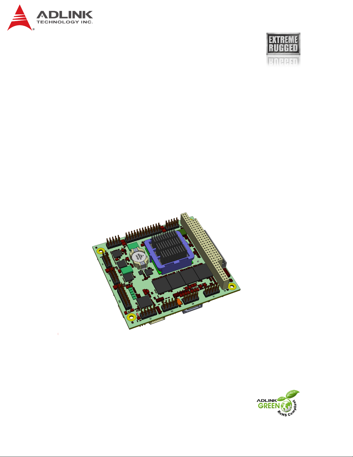
The CM1-86DX2 is a PC/104 Single Board Computer (SBC) based on DMP’s Vortex86-DX2
single chip solution, featuring exceptionally high integration and a very good performance-to-power ratio. The board supports all peripherals needed for an embedded PC on a
small 3.775" by 4.050" printed circuit board.
The Vortex86-DX2 chip integrates a powerful yet efficient CPU with graphics controller, audio
controller, and Gigabit Ethernet controller to form a complete PC, with all the standard peripheral connections onboard.
The board provides two Ethernet ports (1x Gigabit and 1x 100Megabit), four
RS232/RS422/RS485 serial ports, one USB 2.0 host controller, one USB 1.1 host controller to
handle the communication with external devices, and PS/2 connectors for keyboard and
mouse. A first generation SATA interface allows the connection of hard disk or CD drives. Applications that require non-moving storage can use the MicroSD-Card slot or the bootable flash.
System expansion is possible easily over the PC/104, Mini-PCI-Express and I²C bus connectors.
The CM1-86DX2 is powered by a 5V-only supply and runs DOS, Windows XP/7 and Linux
operating systems. The Vortex86-DX2 SoC has a simulated ACPI to support Windows 7
(though S3 or S4 modes are not supported.)
CM1-86DX2
Introduction 1
Page 8
1.2 Features
SoC
DMP Vortex86-DX2 @ max.
1 GHz
X86 Processor Core
Floating point unit support
Embedded I/D L1 Cache
(16K each)
Embedded L2 Cache (256K
4-way)
DDR2 Interface
GPU Control Unit (VGA, 2D
Graphic, UMA Architecture)
Embedded 2MB Flash (BIOS
storage)
Interfaces
1x Ethernet 1GBit
1x Ethernet 100MBit
1x SATA (First Generation)
1x MicroSD(HC)
PS/2 Keyboard/Mouse
4 x USB 2.0 ports (Nr. 4 only with
MiniPCIe extension card)
4 x RS232/RS485
1x LPT
5.1 channel audio (analog &
SPDIF)
1x VGA
Main Memory
1GB DDR2 Memory Down
Extension slots
1x MiniPCIe slot with mSATA
and USB capability (3.3 V I/O)
1x 16-bit PC/104 with full DMA
capability
1x 18/24 Bit LVDS for displays
(alternatively to VGA)
MISC signals: external power
button, I²C bus (3.3 V), speaker
(5 V), external reset button,
external battery connector
8 x Analog input with 10 bit res-
olution and 100 kS/s sampling
rate
1x 8bit GPIO-Port, usable as
TTL-UART
1x JTAG on SIL8, 2.00 mm
pitch
1x Power supply
Other configurations are possible. Please contact your local ADLINK
Technology representative to discuss requirements.
2 Introduction
Page 9
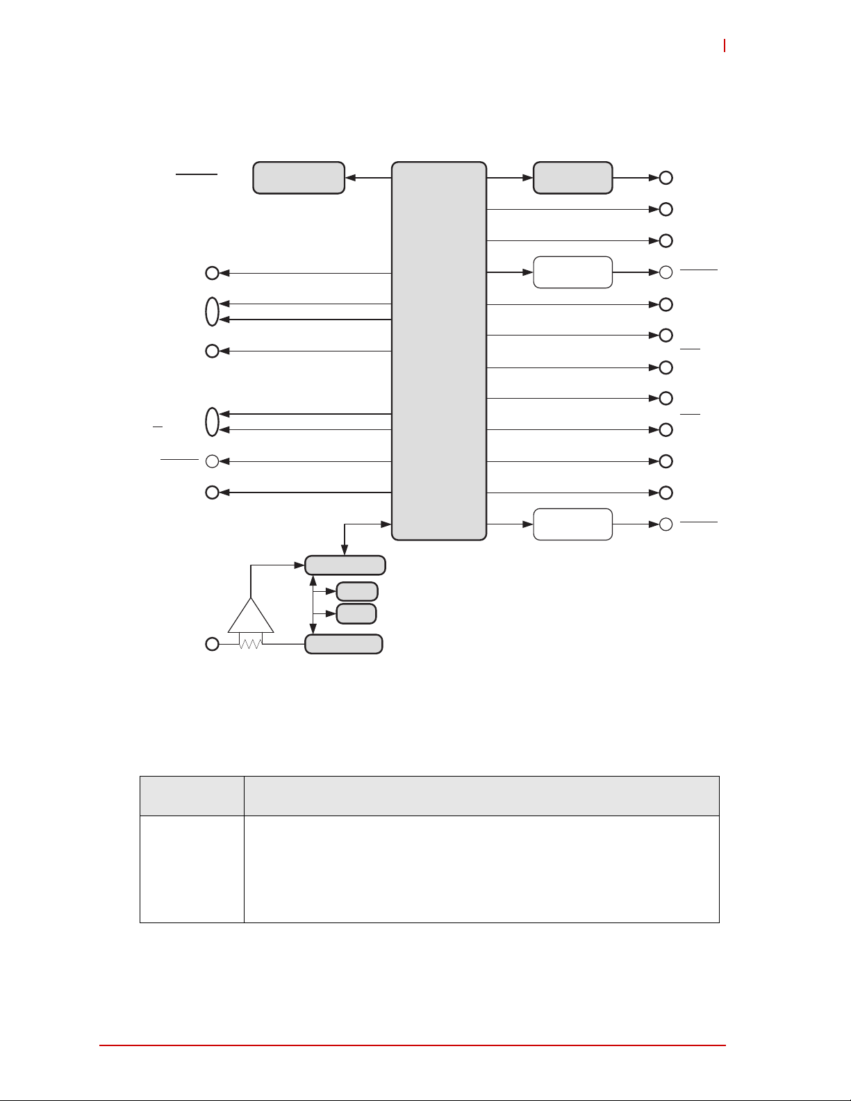
1.3 Block Diagram
Vortex86DX2
ALC886
Audio Codec
SMC / SEMA
DIA G
LM 73
Power Supply
+
-
5VDC
ATX
Stack
I2C
mPCIe or mSATA
ISA
Optional:
HD Audio
RS232/485
PS/2
SATA
Option: SATA or mSATA
LCD
LVD S
VGA
PC/104
Inverter
(Backlight)
2x COM
Option: 4 x COM
Speaker
512MB DDR2-400
Memory Down
VGA
LPT
I2C
8x A/D Input
ADC
I2C
DS90C385A
LCD to LV DS
JTAG
8x GPIO
3x USB 2.0
Optional:
MicroSD Socket
i210IT
Ethernet
PCIe
Optional:
GbE
ETH
PCIe
1x USB 2.0
Optional:
1GB DDR2-400
CM1-86DX2
CM1-86DX2
Figure 1-1: Module functional block diagram
1.4 Ordering Information
Order number Description
702-0018-10
CM1-86DX2 PC/104 CPU board with DMP Vortex86-DX2, including
heat sink, and 1GByte of memory.
Operating temp. range: -0°C … +60°C
CPU clock: 1 GHz
Memory clock: 333 MHz
Table 1-1: CM1-86DX2 Models
Introduction 3
Page 10
802-0018-10
Table 1-1: CM1-86DX2 Models (Continued)
CM1-86DX2 PC/104 CPU board with DMP Vortex86-DX2, including
heat sink, and 1GByte of memory.
Operating temp. range: -20°C … +70°C
CPU clock: 1 GHz
Memory clock: 333 MHz
CM1-86DX2 PC/104 CPU board with DMP Vortex86-DX2, including
heat sink, and 1GByte of memory.
902-0018-10
Operating temp. range: -40°C … +85°C
CPU clock: 800 MHz
Memory clock: 300 MHz
CM1-DX2 PC/104 CPU board with DMP Vortex86-DX2 incl. heat
sink, 512 MByte Memory
702-0020-10
Operating temp. range: -0 °C … +60°C
CPU clock: 1 GHz
Memory clock: 333 MHz
CM1-DX2 PC/104 CPU board with DMP Vortex86-DX2 incl. heat
sink, 512 MByte Memory
802-0020-10
Operating temp. range: -20 °C … +70°C
CPU clock: 1 GHz
Memory clock: 333 MHz
CM1-DX2 PC/104 CPU board with DMP Vortex86-DX2 incl. heat
sink, 512 MByte Memory
902-0020-10
Operating temp. range: -40 °C … +85°C
CPU clock: 800 MHz
Memory clock: 333 MHz
Table 1-2: Cable Sets and Accessories
Order number Description
Adapter Cable Set:
763-0024-10
Power, GBit-Ethernet, Ethernet + USB, VGA-CRT, 2x USB,
COM1…4, 1x SATA, HD-Audio, PS/2
4 Introduction
Page 11
1.5 Specifications
Electrical Specifications
Supply voltage:
Rise time:
CM1-86DX2
Table 1-3: Electrical Specifications
+5 V DC
+5 V standby (only needed for suspend mode)
+12 V (only needed for LVDS display and expansion
slots)
< 10 ms
Supply voltage tolerance:
Inrush current:
Supply current:
Environmental Specifications
Temperature range
Temperature change
Humidity (relative)
Pressure
Table 1-5: Non-Operating/Storage/Transport
Temperature range
Temperature change
± 5%
1.6 A
max. 1.7 A (Windows XP, PIcalc [lots of decimals of
PI]) ; typical 1.5A
Table 1-4: Operating
0°C … 60°C (standard version)
-20°C … 60°C (industrial version)
-40°C … 85°C (extended version)
max. 10 Kelvin per 30 minutes
10 % … 90 % (non-condensing)
450 hPa … 1100 hPa
-40°C … 85°C
max. 10 Kelvin per 30 minutes
Humidity (relative)
Pressure
Cold Temperature Step Stress
5 % … 95 % (non-condensing)
450 hPa … 1100 hPa
Table 1-6: HALT Parameters
The board remained operational during test down to
-100°C, starting at +20°C and decreasing in 10°C
increments with 15 minute dwells
Hot Temperature Step Stress
The board remained operational during test up to
+90°C, starting at +30°C and increasing in 10°C increments with 15 minute dwells
Rapid Thermal Transitions
The board was subject to five rapid temperature cycles
from -90°C to +85°C @ set transition rate of 60°C per
minute
Introduction 5
Page 12
Vibration Step Stress
Combined Environment
MTBF at 25°C
Table 1-6: HALT Parameters (Continued)
The board was subject to vibration step stress with set
points from 5 grams to 45 grams @ 20°C and vibration
increasing by 5 grams with 15 minute dwells at each
level of 2Hz to 5000Hz bandwidth
The board was subject to thermal cycles from -90°C to
+85°C at an average rate of 60°C per minute combined
with vibration at set points of 8, 16, 24, 32, and 40
grams from the first to the fifth thermal cycle and
10-minute dwells at each extreme temperature
Table 1-7: Mean Time Between Failures
TBD
MTBF at 40°C
Mechanical Specifications
Dimensions (L x W)
Height
Weight
Mounting
ADLINK strongly recommends plastic spacers instead of metal spacers for
mounting the board. Metal spacers create the possibilities of short circuits
with the components located around the mounting holes. This can damage
the board.
TBD
Table 1-8: Mechanical
90.6mm x 95.2mm
Max. 31mm on top side above PCB (including heatsink)
98 grams (without MiniPCIe extension card)
4 mounting holes
6 Introduction
Page 13
35.50
81.10
18.31
7.12
6.76
54.81
36.81
72.81
88.75
5
17.36
73.11
62.87
85.62
18.21
44.07
10.43
1.64
8
96
62.92
90
0
2.07
30.03
1.60
42.23
CM1-86DX2_mech_dwg_top_b
CM1-86DX2
Top
9
8.7
Figure 1-2: Mechanical dimensions (top side)
Introduction 7
Page 14
Bottom
74.07
56.68
13.90
4.05
40.10
23.35
53.95
3.50
20.20
70.45
90
17.05
18.60
50.15
96
CM1-86DX2_mech_dwg_top_b
CM1-86DX2_mech_dwg_bottom_a
Figure 1-3: Mechanical dimensions (bottom side)
8 Introduction
Page 15
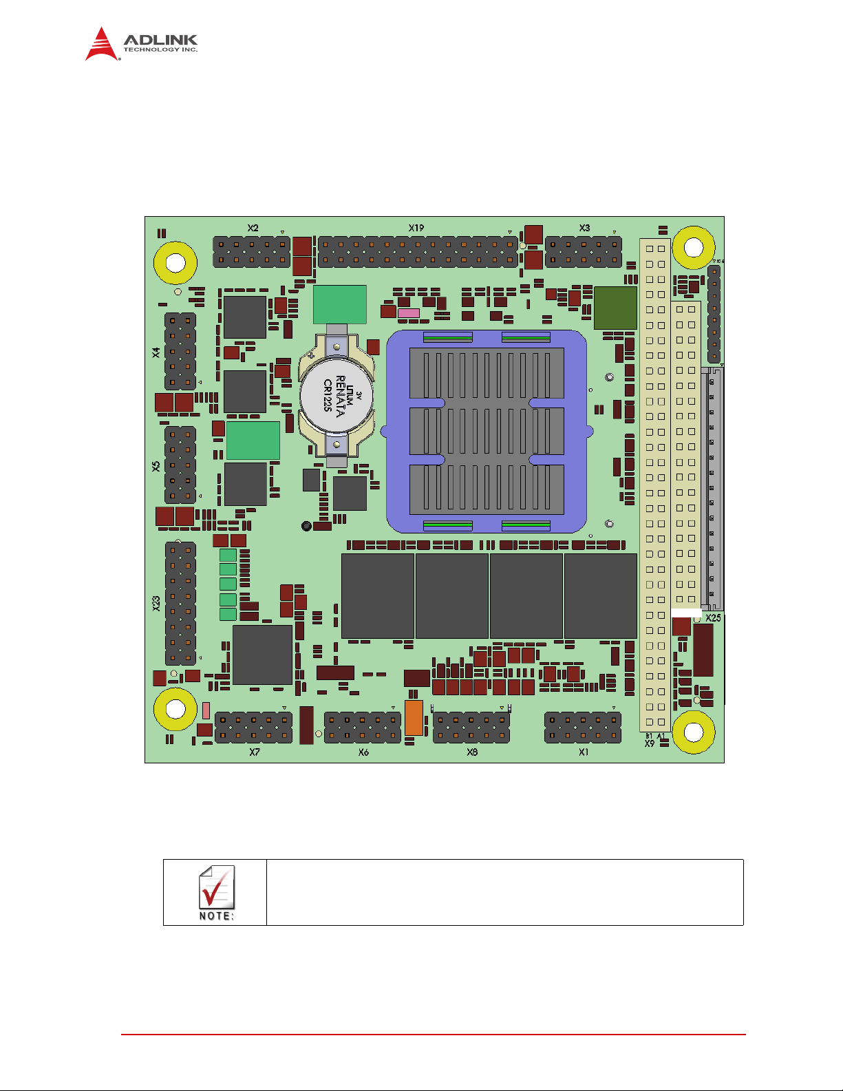
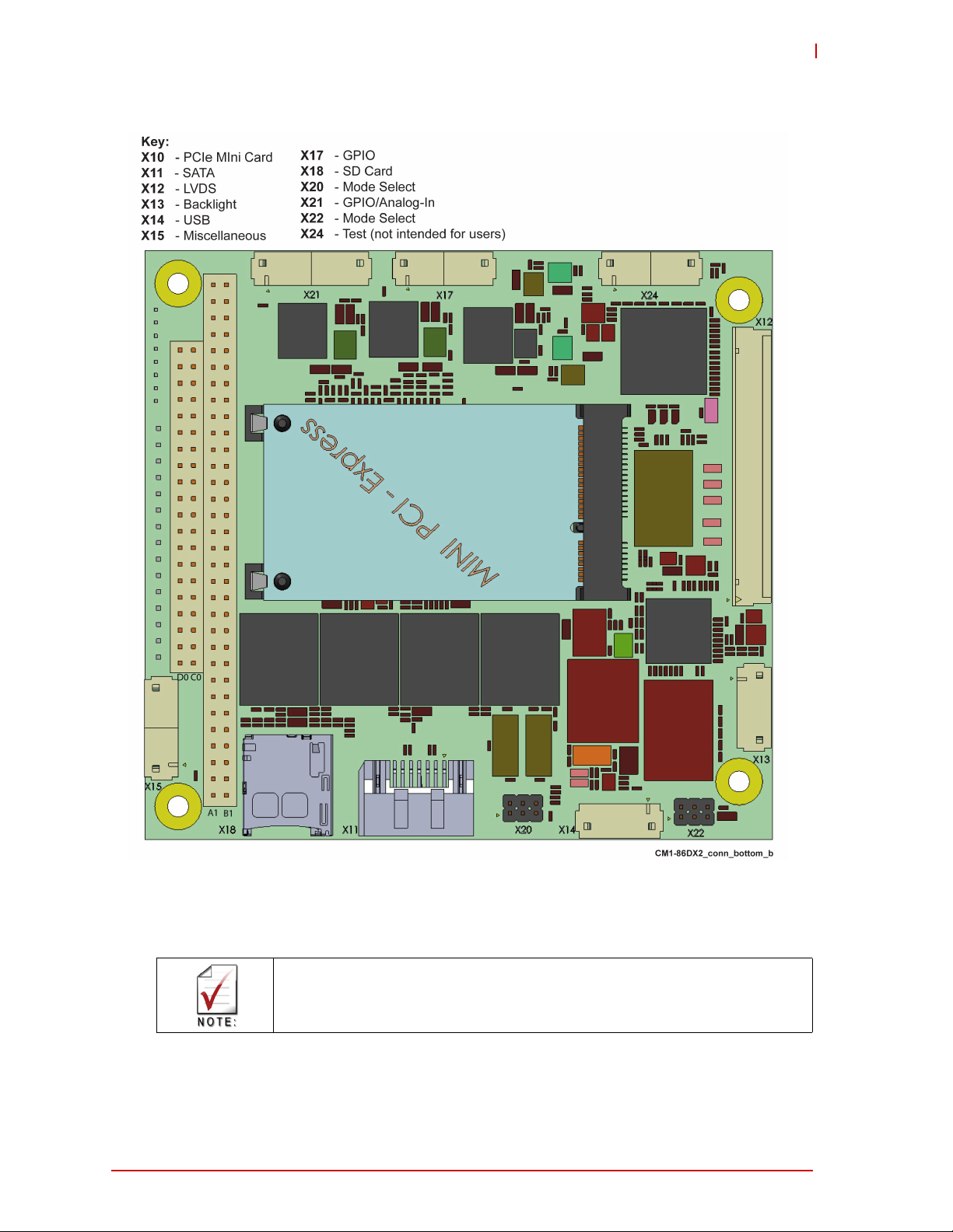
2 Getting Started
2.1 Header and Jumper Locations
Table 2-1 on page 9 provides descriptions of the headers and connectors on the module. The
header and connector locations are shown in Figure 2-1 and Figure 2-2. See Chapter 3 for the
signal definitions of the headers and connectors presented in this table.
Table 2-1: Connector Name and Description
Connector Top/Bottom Description
X1 Top 10-pin, 2.54mm utility header
(AMTEK, PH1M25-205GBCOR600-U)
X2, X3, X4, X5 Top 10-pin, 2.54mm COM headers
(AMTEK, PH1M25-205GBCOR600-U)
X6 Top 10-pin, 2.54mm Gigabit Ethernet header
(AMTEK, PH1M25-205GBCOR600-U)
X7 Top 10-pin, 2.54mm Fast Ethernet header
(AMTEK, PH1M25-205GBCOR600-U)
X8 Top 10-pin, 2.54mm VGA header
(AMTEK, PH1M25-205GBCOR600-U)
X9 Top 104-pin, standard PC/104 connector;
http://www.pc104.org for signal definitions
see
(EPT, 962-60322-12)
X10 Bottom 52-pin standard, PCIe MiniCard connector
(Attend Technology, 119A-92A00-R02)
X11 Bottom 7-pin standard, right-angle SATA connector
(MOLEX, 47080-4001)
X12 Bottom 30-pin, 1.25mm right-angle, single-row LVDS header
(HIROSE, DF14-30P-1.25H)
X13 Bottom 8-pin, 1.25mm right-angle, single-row backlight header
(HIROSE, DF13-8P-1.25H)
X14 Bottom 8-pin, 1.25mm right-angle, single-row USB header [ports 0-1]
(HIROSE, DF13-8P-1.25H)
X15 Bottom 10-pin, 1.25mm right-angle, single-row miscellaneous header
(HIROSE, DF13-10P-1.25H)
X17 Bottom 10-pin, 1.25mm right-angle, single-row GPIO header
(HIROSE, DF13-10P-1.25H)
X18 Bottom 8-pin standard, right-angle SD Card connector
X19 Top 26-pin, 2.54mm LPT parallel port header
(AMTEK, PH1M25-205GBCOR600-U)
X20 Bottom 6-pin, 2mm mode select jumper header
(W+P Products, 7351-06-20-20-60-00)
X21 Bottom 12-pin, 1.25mm right-angle, single-row GPIO and Analog-In
header
(HIROSE, DF13-12P-1.25H)
X22 Bottom 6-pin, 2mm mode select jumper header
(W+P Products, 7351-06-20-20-60-00)
X23 Top 16-pin, Audio header
(PFL-2X8-2M54-SMD)
X24 Bottom 10-pin, 1.25mm right-angle, single-row test header (not
intended for users)
X25 Top 15-pin, 2.5mm single-row, PC/104 ATX power connector
(JST, B15B-EH-A/LF)
CM1-86DX2
Getting Started 9
Page 16
Key:
X1 - Utility
X2, X3,
X4, X5 - COM
X6 - Gigabit Ethernet
X7 - Fast Ethernet
X8 - VGA
CM1-86DX2_conn_top_b
X16
C0 D0
X9 - PC/104
X16 - JTAG
X19 - Parallel
X23 - Audio
X25 - ATX Power
Top
Figure 2-1: Header locations (top side)
The yellow arrows next to the connectors in this illustration denote pin 1.
10 Getting Started
Page 17
Bottom
CM1-86DX2
Figure 2-2: Header locations (bottom side)
The yellow arrows next to the connectors in this illustration denote pin 1.
Getting Started 11
Page 18
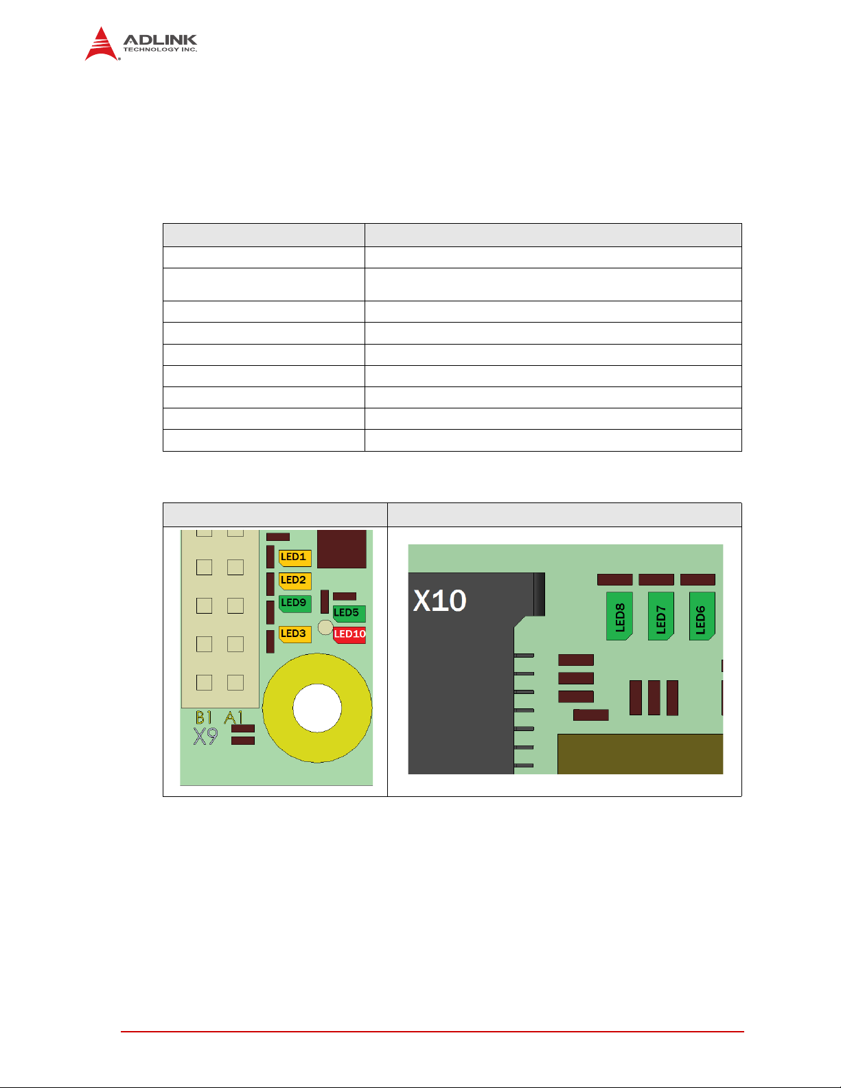
2.2 LED Indicators
The onboard LED indicators provide board status including error codes and Watchdog and
Ethernet statuses.
The MiniPCIe LEDs are located on bottom of the board, near the MiniPCIe connector. All other
LEDs are located near the PC/104 connector on the top.
Table 2-2: LED Name and Description
LED Description
STATUS (LED5, TOP) Green LED shows error codes in terms of failure.
WD (LED10, TOP) Red LED lights up when Watchdog was triggered. Can only be
reset by a power off sequence.
ETH0_LINK_ACT (LED3, TOP) Yellow LED shows link and traffic on Ethernet0 (100 MBit/s)
ETH1_LED_100 (LED9, TOP) Green LED shows 100MBit link on Ethernet1 (1 GBit/s)
ETH1_LED_1000 (LED1, TOP) Yellow LED shows 1GBit link on Ethernet1 (1 GBit/s)
ETH1_LED_ACT (LED2, TOP) Yellow LED shows traffic on Ethernet1 (1 GBit/s)
LED_WWAN (LED6, BOT) Green LED shows WAN status of MiniPCIe card
LED_WLAN (LED7, BOT) Green LED shows LAN status of MiniPCIe card
LED_WPAN (LED8, BOT) Green LED shows PAN status of MiniPCIe card
LED TOP LED BOTTOM
12 Getting Started
Page 19
CM1-86DX2
2.3 Hardware Setup
Be sure to observe the EMC security measures. Make sure you are always at the same
potential as the module.
Never connect or disconnect peripherals like HDDs, PCI, and ISA boards while the board's
power supply is connected and switched on.
Use the cable set provided by ADLINK Technology to connect the CM1-86DX2 to a VGA monitor. Connect either PS/2 or USB keyboard or mouse, respectively. Use the SATA cable to connect the hard disk. Make sure that the pins match their counterparts correctly and are not
twisted. If you plan to use additional peripherals, connect them to the appropriate headers.
Connect a 5 volt, 5 amps power supply to the power connector and switch on the power.
The 5 amps value is the minimum you should have for the standard peripherals
mentioned. For additional peripherals, make sure enough power is available. The
system will not work if there is not enough supply current for all your devices.
The display shows the BIOS messages. If you want to change the standard BIOS settings,
press the <DEL> key to enter the BIOS menu. See “Using the Module” on page 43 for setup
details.
If you need to load the BIOS default values, they can be automatically loaded at boot time.
The CM1-86DX2 boots from CD drives, USB floppy, USB stick, hard disk or µSD-Card. Provided
that any of these is connected and contains a valid operating system image, the display then
shows the boot screen of your operating system.
The CM1-86DX2 needs adequate cooling measures depending on the desired operating temperature range. Using the board without cooling could damage the board permanently.
Getting Started 13
Page 20

14 Getting Started
Page 21
3 Module Description
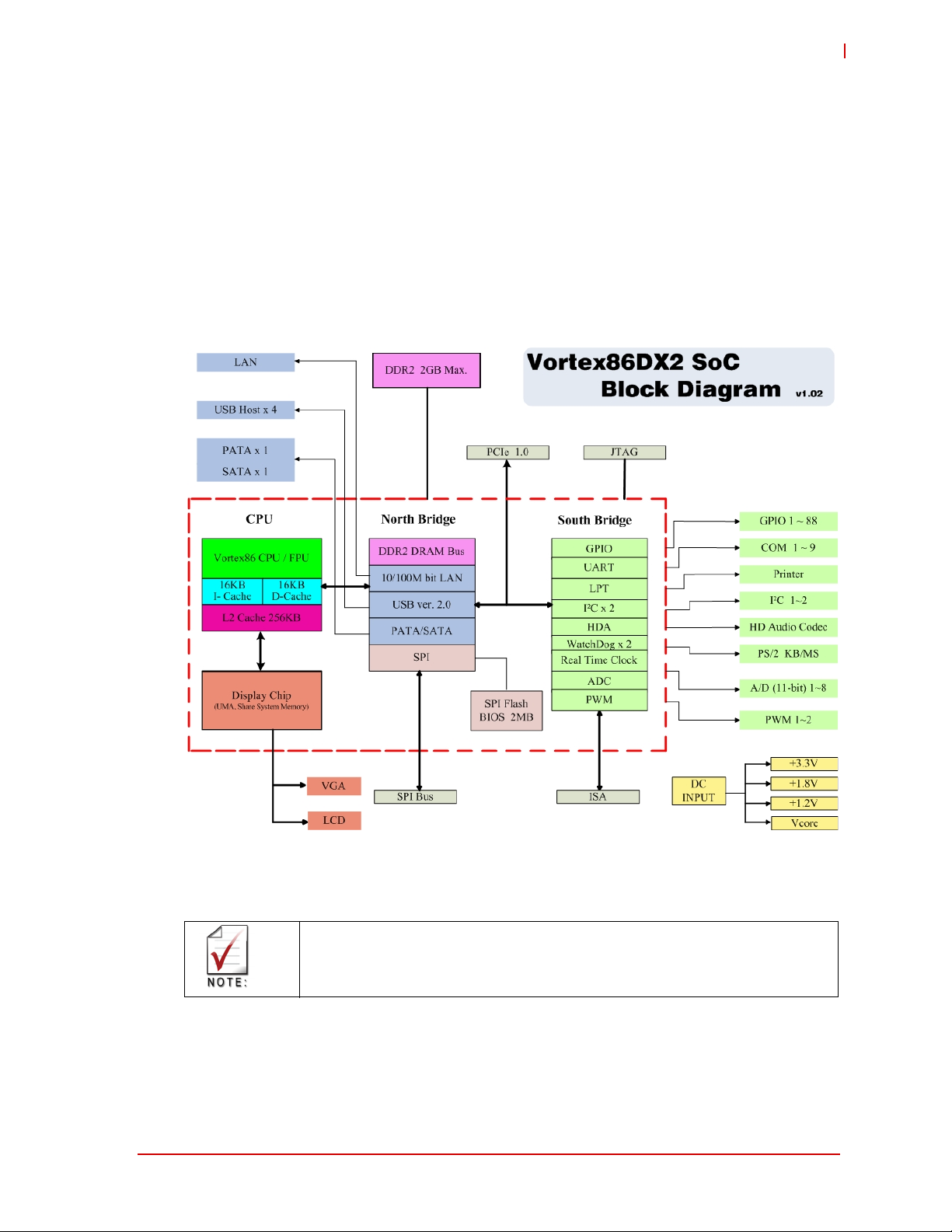
3.1 Processor and Chipset (SoC: System on a Chip)
The Vortex86DX2 is a high performance and fully static 32-bit x86 processor with the compatibility of running Windows, Linux, and most popular 32-bit Real-Time Operating Systems. It also
integrates 32KB write through 4-way L1 cache, 256KB write-through/write-back 4-way L2
cache, PCIE bus in at 2.5Gb/s, DDR2, ROM controller, ISA, I2C, SPI, IPC (Internal Peripheral
Controllers with DMA and interrupt timer/counter included), Fast Ethernet, FIFO UART, USB2.0
Host, IDE/SATA controller and two Watchdog Timers within a single 720-pin BGA package to
form a system-on-a-chip (SoC). The SoC provides an ideal solution for embedded system and
communications products such as thin clients, NAT routers, home gateways, access points, and
tablet PCs.
CM1-86DX2
Figure 3-3: CPU functional block diagram
The two-row headers on the this board all use a pin sequence in which one
row is odd numbered and the adjacent row is even numbered.
Module Description 15
Page 22

3.2 Processor functional blocks
The processor part in the Vortex86DX2 consists of the following components:
CPU Core
Northbridge
Southbridge
Graphics Controller for VGA or LVDS
Ethernet Controller
IDE / SD / SATA Controller
2x USB2.0 / USB1.1 Controller
BIOS flash
For further information, please refer to the datasheet of the DMP Vortex86DX2 SoC.
3.3 Graphics Controller
This section lists the features of the Vortex86DX2 SoC integrated graphics engine.
VGA Features
Fully IBM VGA compliant
Resolutions up to 1920x1440
One dedicated PLL for video clock generation
2D graphics support
Supports 64 x 64 hardware overlay cursor with mono and color formats
RGB analog output
Up scaling
Scaling down, display resolution 1024x768 support
Supports 8-Bit DAC
UMA architecture
32MB graphics ram (from the main memory, to configure via the BIOS)
Supports VESA DDC
Supports LVDS mode with one 18-bit TTL, one 12-bit DDR Mode or one 24-bit SDR Mode
16 Module Description
Page 23

2D Features
Directly access data through M-Bus
High performance pipe-lined, one-cycle 64-bit 2D graphics engine
2D engine commands:
BitBlt Rectangle Fill
BitBlt Pattern Fill
BitBlt Rectangle Copy from Source to Destination
Support 256 Raster Operations
Integrate 8x8 Pattern Registers
Integrate 8x8 Mask Registers
Support Rectangle Clip
Support Color Expansion
Support Enhanced Color Expansion
Support Line Drawing with Style Pattern
Support Line Setup
Transparent BitBlt
Alpha Blending
Stretch and Shrink BitBLt
Gradient fill
Anti-Aliased Test
Pattern offset
Mono Source form system memory
2D rotation, display resolution 1024x1024 support
Programmable 256K/512K/1M/2M off-screen command buffer
Integrated 32 stages of hardware command queue for 2D command pre-fetch from off-
screen memory space of frame buffer
Integrated 32x64 source buffer and destination buffer to improve 2D engine performance
Integrated 32x98 post-write buffer to improve 2D engine performance
CM1-86DX2
DMA Features
Supports system memory to video memory and vice versa
Maximum transfer byte count per one command is 4 Mbyte
One interrupt signal
One 16x64 data FIFO for system memory to frame buffer
One 16x64 data FIFO for frame buffer to system memory
Byte alignment
Chaining mode only
Video Display Features
Supports Up-Scaling
Supports Color Key and Chroma Key
Supports Hardware Icon
Module Description 17
Page 24

Power Management Features
Supports VESA Display Power Management Signaling (DPMS) compliant VGA monitor
for power management
Supports direct I/O command to force graphics accelerator into standby/suspend-off state
Video Post-Processor Features
Up/Down-Scaling
De-Interlace (Bob and Weave mode)
3:2 Sequence Pull-Down Detection
Color Space Enhance and Conversion
Image Cropping (Source Rectangle)
Sub-Picture (AI44 or AYUV) Blending with main video
Video rotation
Capture Features
Supports 8 bit BT.656 to frame base xRGB888
Supports Input YUV format : YUYV or UYVY
YUV2RGB function can be disabled
Software clear capture interrupt
BT.656 use header information to setting VBI or ANC capture range
3 active video frame buffer
2 VBI or ANC frame buffer
Programmable color space conversion coefficient
Supports coring function
Supports minify
Command Queue Features
Programmable max. 8M off-screen command queue buffer
8-bytes aligned command queue data
Supports multi-command types
Null Command
Single Command for 2D, DMA, VPOST, VDISP
Burst Command for 2D only
Source In Queue(SIQ) Command for 2D only
Command queue is ring structure
Programmable writer-pointer for updating command queue data
Readable read-pointer for 2D, DMA, VPOST, VDSIP Graphics Engine has read command
queue data
18 Module Description
Page 25

VGA Header (X8)
Connector type: DC10 pin header 2.54 mm
Adapter cable
Pin Signal Pin Signal
1Red 2GND
3Green 4GND
5 Blue 6 VGA_DDC_CLK
7 HSYNC 8 VGA_DDC_DATA
9 VSYNC 10 GND
: Article number 862-0008-11
Table 3-1: VGA Header Signals (X8)
CM1-86DX2
LVDS Configuration
The onboard voltage jumper headers allow you to select the display and backlight supply voltages. (See Table 3-4 on page 23 for Display and Backlight Voltage jumper signals.)
LVDS support can be configured within the BIOS. Using LVDS disables the VGA port on the
CM1-86DX2. You can use a CRT or an LVDS panel only exclusively from each other.
You can switch the video output at startup by pressing the “c”-Key for CRT-mode and
the “t”-Key for LVDS-mode.
Module Description 19
Page 26

LVDS Color Mapping
20 Module Description
Page 27

LVDS Header (X12)
Connector type: Hirose DF14 30-pin header
Adapter cable
Pin Signal Pin Signal
1 VCC_LCD 2 VCC_LCD
3 GND 4 GND
5 LVDS_L3n 6 LVDS_L3p
7 LVDS_LCLKn 8 LVDS_LCLKp
9 GND 10 LVDS_L2n
11 LVDS_L2p 12 LVDS_L1n
13 LVDS_L1p 14 LVDS_L0n
15 LVDS_L0p 16 GND
: n/a
Table 3-2: LVDS Header Signals (X12)
CM1-86DX2
17 n. c. 18 n. c.
19 n. c. 20 n. c.
21 GND 22 n. c.
23 n. c. 24 n. c.
25 n. c. 26 n. c.
27 n. c. 28 GND
29 reserved 30 reserved
The maximum current on all supply pins is 1A.
Module Description 21
Page 28

Backlight Header (X13)
Connector type: Hirose DF13 8-pin header
Adapter cable
Pin Signal Pin Signal
1 +12 V 2 +12 V
3+5 V 4+5 V
5 EN 6 VCC*
7GND 8GND
: n/a
Table 3-3: Backlight Header Signals (X13)
*This voltage can be selected using the jumper "Backlight", shown on next table.
The maximum current on all supply pins is 1A.
22 Module Description
Page 29

Display Voltage Jumpers (X22)
Jumper LVDS and Backlight Power Supply
Connector type
Use a 2 mm jumper between 1-3 or 3-5 to select the backlight voltage.
Use a 2 mm jumper between 2-4 or 4-6 to select the display voltage.
Pin Signal (Backlight) Pin Signal (LVDS)
1 +12V 2 +3.3V
3 Backlight Voltage 4 Display Voltage
5 +5V 6 +5V
: DC6 pin header 2.00 mm
Table 3-4: LVDS and Backlight Voltage Jumper Signals (X22)
Default jumper positions
CM1-86DX2
3.4 Ethernet Controllers
Two Ethernet controllers reside on the module. A 100 Mbit Ethernet Controller is implemented in
the Vortex86-DX2 SoC. A second Controller (Intel i210) provides GBit Ethernet functionality.
Features of the 10/100 Mbit Controller
Integrated Fast Ethernet MAC and PHY
10 Mbps and 100 Mbps operation
Supports 10 Mbps and 100 Mbps N-way Auto-negotiation
PCI local bus single-chip Fast Ethernet
Provides PCI bus master data transfers
PCI memory space or I/O space mapped data transfer of operational registers
Supports digital and analog loop back capability
Half/Full duplex capability
Supports Full Duplex Flow Control in compliance with IEEE 802.3x
Module Description 23
Page 30

Features of the 10/100/1000 Mbit controller
IEEE 802.3 compliant
Auto Negotiation
Audio-Video bridging
IEEE 1588/802.1AS precision time synchronization
IEEE 802.3Qav traffic shaper (with software extensions)
Jumbo Frame support
Interrupt moderation, VLAN support, IP checksum off load
Four transmit and four receive queues
Advanced cable diagnostics, auto MDI-X
ECC – error correcting memory in packet buffers
IEEE 802.3az Energy Efficient Ethernet (EEE)
Wake-on-LAN
100 Mbit Ethernet Connector (X7)
Connector type: IDC10 pin header 2.54 mm
Adapter cable
: Article number 862-0005-10
Table 3-5: Fast Ethernet Header Signals (X7)
Pin Signal Pin Signal
1 ETH0_TXp 2 ETH0_TXn
3 ETH0_RXp 4 ETH0_PE
(Protection Earth for
shielded Ethernet
cables)
5 NC 6 ETH0_RXn
7* USB2_p 8* USB2_n
9 +VCC_USB2 10 GND_USB2
*The CM1-86DX2-512 model does not offer the USB function on the X7 connector.
24 Module Description
Page 31

Gbit Ethernet Connector (X6)
Connector type: DC10 pin header 2.54 mm
Adapter cable
1ETH1_MX0n 2ETH1_MX0p
3ETH1_MX1n 4ETH1_MX1p
: Article number 862-0088-10
Table 3-6: Gbit Ethernet Header Signals (X6)
Pin Signal Pin Signal
CM1-86DX2
5 ETH1_PE (Protection
Earth for shielded
Ethernet cables)
7ETH1_MX2n 8ETH1_MX2p
9 ETH1_MX3n 10 ETH1_MX3p
6n. c.
3.5 On-Board Power Supply
The on-board power supply generates all necessary voltages from the single supply voltage of
5 volts. The generated 3.3 volts are available on the connectors “Flat Panel”, “LVDS” and
“AnalogIn”.
This 3.3V must not be used to supply external electronic devices with high power
consumption like other PC/104 boards or displays.
Module Description 25
Page 32

Power Connector (X25)
Connector type: JST B15B-EH-A 15 pin
Adapter cable
Pin Signal (standard) Signal (5V only)
1+5V +5V
2GND GND
3+5V +5V
4GND GND
5+5V +5V
6 +5V Standby NC
7GND GND
8 PSON# GND
9PWROK NC
10 NC NC
11 GN D GN D
12 +12V (only for PC104 slot and backlight
13 +12V (only for PC104 slot and backlight
14 GND GND
15 -12V (only for PC104 slot) NC
: Article number 862-0044-10
Table 3-7: Power Connector Signals (X25)
NC
power supply)
NC
power supply)
The default cable adapter supports the connection of 12V power supply. If the 5V only
power supply is required, leave these pins open. The board can also be supplied over the
PC/104 bus.
Real Time Clock Backup (BAT1)
A battery is integrated on board. This battery is necessary to power the real-time clock (RTC) if
the power supply is switched off.
Battery Type
26 Module Description
: CR1225, 3 Volt
Page 33

CM1-86DX2
3.6 IDE / SD / SATA Controller
The integrated Serial ATA controller processes host commands and transfers data between the
host and Serial ATA devices. With respect to the transfer rate, the integrated SATA controller
supports first generation SATA (1.5 Gbit/s). The CM1-86DX2 provides one SATA connector
(X11) for connecting a SATA disk drive or an optical SATA drive.
The MicroSD-Card is driven as an IDE drive and has no
hot-plug capability.
An mSATA device can be connected at the MiniPCIe socket (X10) but the mSATA device will
use the SATA controller exclusively, and no external SATA device will function.
The SATA controller can operate in two modes:
SATA in legacy mode
SATA in native mode (default setting)
IDE-Controller Features
Compatible with the ATA/ATAPI-6 specification and supports two IDE channels with up to
four drives
Programmable active pulses and recovery time for data port access timing
512 bytes FIFO for data transfer per IDE channel
Supports Scatter/Gather function for DMA/UDMA transfer
PCI-Interface
complies with PCI local bus specification revision 2.2
supports PCI Power Management v1.1 capability
supports one Flash/ROM interface for expansion ROM of PCI card
Module Description 27
Page 34

SATA Connector (X11)
Connector type: SATA
Adapter cable
1GND
2 Data_TX+
3 Data_TX-
4GND
5 Data_RX-
6 Data_RX+
7GND
: n/a
Pin Signal
MicroSD Connector (X18)
Connector type: MicroSD
Table 3-8: SATA Connector Signals (X11)
Table 3-9: MicroSD Connector Signals (X18)
Pin Signal
1D2
2D3
3CMD
4VDD
5CLK
6GND
7D0
8D1
28 Module Description
Page 35

CM1-86DX2
Utility Header (X1)
The Utility header is shared with PS/2 mouse and keyboard, Speaker, Reset Switch, Power Button, and Battery. An adapter cable for the PS/2 devices is available.
Connector type
Adapter cable
Pin Signal Pin Signal
1 Speaker 2 Mouse Clock
3 Reset-In 4 Mouse Data
5 KB Data 6 KB Clock
7 GND 8 +VCC_PS2
: IDC10 pin header 2.54 mm
: Article number 862-0004-10
Table 3-10: PS/2 Keyboard and Mouse Signals (X1)
9 Ext. Battery 10 Power Button
External Battery
A connected external battery should replace or support the mounted one to keep date and time.
It is recommended to use a 3-volt model (CR1225). The time and date will be lost if the power
supply falls to 2.5 volts.
For battery-life calculation (worst case), 3 µA (25°C) are required when the board is not running.
That value can rise depending on the connected cables and higher temperatures.
Table 3-11: External Battery Signals (X1)
Pin Signal Pin Signal
1 Speaker 2 Mouse Clock
3 Reset-In 4 Mouse Data
5 KB Data 6 KB Clock
7GND
9 Ext. Battery
8 +5V Standby
10 Power Button
Module Description 29
Page 36

Power Button
To power up/down the board, the signal Power Button must be pulled to GND.
Table 3-12: Power Button Signals (X1)
Pin Signal Pin Signal
1 Speaker 2 Mouse Clock
3 Reset-In 4 Mouse Data
5 KB Data 6 KB Clock
7GND 8 +5V Standby
9 Ext. Battery 10 Power Button
Reset Switch
To reset the CPU using a reset switch, the Reset Switch signal must be pulled to GND.
Table 3-13: Reset Switch Signals (X1)
Pin Signal Pin Signal
1 Speaker 2 Mouse Clock
3 Reset-In
5 KB Data 6 KB Clock
7GND 8 +5V Standby
9 Ext. Battery 10 Power Button
4 Mouse Data
Speaker
A standard PC Speaker can be connected between the signals Speaker and +5V Standby.
Table 3-14: Speaker Signals (X1)
Pin Signal Pin Signal
1 Speaker 2 Mouse Clock
3 Reset-In 4 Mouse Data
5 KB Data 6 KB Clock
7 GND 8 +5V Standby
9 Ext. Battery 10 Power Button
30 Module Description
Page 37

CM1-86DX2
3.7 USB 2.0 Ports
The Vortex-86DX2 contains one Enhanced Host Controller Interface (EHCI) host controller,
which supports up to four USB 2.0 high-speed root ports. USB 2.0 allows data transfers up to
480Mb/s using the same pins as the four USB full-speed/low-speed ports. The Vortex-86DX2
contains port-routing logic that determines whether a USB port is controlled by the UHCI controller or by the EHCI controller.
The CM1-86DX2 uses three of the four ports. They are available on two USB connectors, one
providing two ports and one providing one port. USB 2.0 supports a USB keyboard running
under MSDOS without special driver software.
The fourth USB port is routed to the MiniPCIe socket X10 and requires a USB extension card.
The maximum current on all supply pins is 0.5A.
Not all USB keyboard models are supported.
USB 2.0 Ports 0-1 Header (X14)
Connector type: Hirose DF13 8 pin
Adapter cable
1 VCC_USB01
2 USB0_n
3 USB0_p
4 GND_USB01
5 GND_USB01
6 USB1_n
7 USB1_p
8 VCC_USB01
: Article number 862-0058-10
Table 3-15: USB Ports 0-1 Signals (X14)
PIN Signal
Module Description 31
Page 38

USB 2.0 Port 2 Header (X7)*
Connector type: DC10 pin header 2.54 mm
Adapter cable
Pin Signal Pin Signal
1 ETH0_TXp 2 ETH0_TXn
3 ETH0_RXp 4 ETH0_PE
5 NC 6 ETH0_RXn
7* USB2_p 8* USB2_n
9 +VCC_USB2 10 GND_USB2
: Article number 862-0088-10
Table 3-16: USB Port 2 Signals (X7)
*The CM1-86DX2-512 model does not offer the USB function on the X7 connector.
3.8 HD-Audio
The High Definition (HD) Audio Controller communicates with the external HD Audio codec over
the HD Audio Link. The HD Audio Controller consists of four independent output DMA engines
and four independent input DMA engines that are used to move data between system memory
and the external codec.
The CM1-86DX2 uses a codec from Realtek. The ALC886 is a high-performance 7.1+2 Channel
High Definition Audio Codec.
The following I/Os are used by the CM1-86DX2:
Analog Input (All ADC support 44,1 kHz, 48 kHz, 96 kHz, and 192 kHz sampling rates)
Microphone left and right
Line In left and right
Analog output (All ADC support 44,1 kHz, 48 kHz, 96 kHz, and 192 kHz sampling rates)
Front left and front right
Rear left and rear right
Center and subwoofer
Digital input (16/20/24-bit S/PDIF-in support 44,1 kHz, 48 kHz, 96 kHz, and 192 kHz sam-
pling rates)
S/PDIF
Digital output (16/20/24-bit S/PDIF-out support 44,1 kHz, 48 kHz, 96 kHz, and 192 kHz
sampling rates)
S/PDIF
32 Module Description
Page 39

Audio Header (X23)
Connector type: DC16 pin header, 2.54mm
Adapter cable
Pin Signal Pin Signal
1 LineOut_R 2 LineOut_L
3 Surround_R 4 Surround_L
5 LFE 6 Center
7 GND_Audio 8 GND_Audio
9 LineIn_R 10 LineIn_L
11 MIC_R 12 M IC_L
13 GND 14 GND
15 S/P_DIF_IN 16 S/P_DIF_OUT
: Article number 862-0086-10
Table 3-17: Audio Header Signals (X23)
CM1-86DX2
Module Description 33
Page 40

3.9 Serial Ports
Each of the four serial ports is located on one dedicated IDC header (COM1-4.) The ports either
work in RS232 or RS485 modes
application. Termination resistors for RS485 Mode must be set by a DIPSwitch (SW1 or SW2).
To enable the transmitters of COM1 through COM4 in RS485 mode set the RTS# signal to ‘1’.
Depending on your operating system driver’s logic, this may mean setting a (non-inverted) RTS
bit to ‘0’ in your application software.
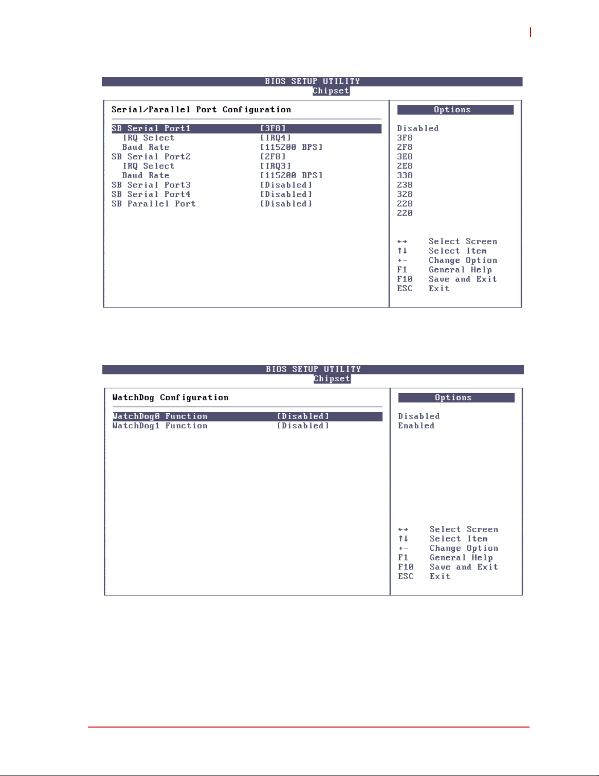
The serial ports are programmable in BIOS setup:
ADVANCED>CHIPSET>SouthBridge Configuration>Serial/Parallel Port Configuration
The following settings for COM1 through COM4 are available in BIOS setup:
Serial Port: enabled / disabled
Base address: 3F8h / 2F8h / 3E8h / 338h / 2E8h / 238h / 328h / 228h / 220
IRQ: 3 / 4 / 5 / 6 / 7 / 9 / 10 / 11 / 12 / 14 / 15
Bits per Second: 2400 / 4800 / 9600 / 19200 / 38400 / 56700 / 115200
The default values are:
COM1 enabled, 3F8h, IRQ4
COM2 enabled, 2F8h, IRQ3
COM3 disabled
COM4 disabled
The maximum supported baud rates are:
, selectable in the BIOS (modification required) or with a user
0.75 Mbit/s in RS485 high speed mode
115.2 Kbit/s in RS232 mode
The baud rates can be configured by the user application.
Utility COM Ports
The CM1-86DX2 provides some extra connectivity for an LV-TTL-UART interface (COM6.) More
information on COM6 can be found in the User GPIO (X17) section and Analog-In (X21) about
GPIOs, which are shared with COM6. COM6 does not provide a transceiver and only RX and
TX signals are present.
COM Headers: Ports 1, 2, 3, 4 (X2, X3, X4, X5)
Connector type: DC10 pin header 2.54 mm
Adapter cable
Pin RS232 RS485/422 Pin RS232 RS485/422
1 DCD Not used 2 DSR RXD+
3 RXD RXD- 4 RTS TXD+
5 TXD TXD- 6 CTS Not used
7 DTR Not used 8 RI Not used
9 GND GND 10 +5.0 V +5.0 V
: Article number 862-0046-10
Table 3-18: COM Ports 1-4 Signals (X2, X3, X4, X5)
34 Module Description
Page 41

CM1-86DX2
The maximum current on all supply pins is 0.5A.
RS485/422 Termination
Typically the RS485 cabling is done as a bus system with two or more devices on the bus. The
cabling can be done in 4-wire mode (RX+, RX-, TX+, TX- using 4 independent wires) or 2-wire
mode (RX+, TX+ and TX-, RX- are using 2 wires). In RS485 Mode the differential pairs should
be terminated with 120 Ω if the device is located at the beginning or end of the bus.
The termination is done by switching the appropriate sliders on the DIP-Switch from the off positions to on positions. So COM1 and COM3 use positions 1 & 2 each, and COM2 and COM4 use
positions 3 & 4 each of the DIP-Switch (SW2 and SW1).
When the termination is set, the differential pairs are terminated with 120 Ω between them (e.g.
RX+ and RX-, in the following illustration.)
Additionally, positive/negative receive lines are pulled up/down with 10 kΩ to 5V/GND in order to
protect the transceivers of the CM1-86DX2 from overvoltage.
It is recommended to protect the ports of the external device in the same way.
Termination resistors should not be used in RS232 Mode. Otherwise, the serial ports will
not work.
Module Description 35
Page 42

3.10 LPT Interface (X19)
The parallel port is located on an IC26 header. An adapter cable with standard DSUB-25 female
connector is available. The parallel port is programmable in BIOS. Enter ADVANCED>CHIPSET>Southbridge Configuration>Serial/Parallel Port Configuration for access to the following
settings.
Table 3-19: BMC Service Connector (X24)
LPT Parameter Possible Settings
Base Address Disabled, 0x378 and 0x278
Mode BPP, EPP 1.9 and SPP, ECP, ECP and EPP 1.9, SPP, EPP 1.7 and SPP, ECP
and EPP 1.7
IRQ Disabled, IRQ 3, IRQ 4, IRQ 5, IRQ 6, IRQ 7, IRQ 9, IRQ 10, IRQ 11, IRQ 12,
IRQ 14 and IRQ15
LPT Header (X19)
Connector type: IDC26 pin header, 2.54 mm (X19)
Matching connector
Pin Signal Pin Signal
1 Strobe 2 Auto LF
3 Data0 4 Error
5 Data1 6 Init
7 Data2 8 Select In
9 Data3 10 GND
11 Data4 12 GND
13 Data5 14 GND
15 Data6 16 GND
17 Data7 18 GND
19 ACK 20 GND
21 busy 22 GND
23 Paper End 24 GND
: IDC26 pin female connector, 2.54 mm
Table 3-20: LPT Header Signals (X19)
25 Select 26 +5.0 Volt
The maximum current on all supply pins is 0.5A.
36 Module Description
Page 43

3.11 MiniPCI-Express Interface (X10)
Connector type: MiniPCIe/MiniCard socket/mSATA socket
Table 3-21: MiniPCIe Interface (X10)
Pin Signal Pin Signal
1 n.c. 2 3.3 V
3n.c. 4GND
5 n.c. 6 1.5 V
7CLKREQ# 8n.c.
9GND 10n.c.
11 PCIE1_CLK_n 12 n.c.
13 PCIE1_CLK_p 14 n.c.
15 GND 16 n.c.
Mechanical Key
17 Reserved 18 GND
19 Reserved 20 n.c.
21 GND 22 PERST#
23 PCIE1_RX_n 24 3.3 V
25 PCIE1_RX_p 26 GND
27 GND 28 1.5 V
29 GND 30 I2C0_CLK
31 PCIE1_TX_n 32 I2C0_DATA
33 PCIE1_TX_p 34 GND
35 GND 36 USB3_n
37 GND 38 USB3_p
39 3.3 V 40 GND
41 3.3 V 42 LED_WWAN#
43 GND 44 LED_WLAN#
45 Reserved 46 LED_WPAN#
47 Reserved 48 1.5 V
49 Reserved 50 GND
51 Reserved 52 3.3 V
CM1-86DX2
The MiniPCIe-Card-Socket can also be equipped with an mSATA-Card. Therefore, the mSATACard has to pull Pin 43 up, while Pin 21 or Pin 51 has to be pulled down.
If Pin 43 is pulled low, while Pin 21 or Pin 51 is pulled low, the normal mini card functionality is
maintained.
In cases where the auto detection of the card type fails, you can force the mode of operation
with the jumper header X20.
Module Description 37
Page 44

MiniPCIe-Card-Mode Jumper Header (X20)
The default setting is the automatic detection mode (shown below), where pins 3-4 are connected. To force mini card operation, pins 5-6 must be connected. The mSATA mode is forced
by connecting pins 1-2 on the jumper block X20.
Table 3-22: PCIe Mini Card Jumper Signals (X20)
Pin Signal Pin Signal
1 +3.3V S 2 SSD-SEL
3 Detection from socket 4 SSD-SEL
5 GND 6 SSD-SEL
Depending on the board used in the Mini PCI Express socket, the automatic switching
between Mini PCI Express and mSATA mode may malfunction. If malfunction occurs,
use Force Mode to switch between mSATA and Mini PCI Express.
3.12 PC/104 Bus Interface
The PC/104 bus is a modification of the industry standard (ISA) PC bus specified in IEEE P996.
The PC/104 bus has different mechanics than P996 to allow for stackable modules. The main
PC/104 features are:
Support for programmable extra wait state for ISA cycles
Support for I/O recovery time for back-to-back I/O cycles
The following table shows the pin assignment of the PC/104 connector.
-5 V on the PC/104 connector are not supported on this board.
The voltages +5V, +12V, and -12V are not generated by the onboard power-supply but
routed from the Power Supply Connector. The maximum current is limited to 1.0A for
each voltage.
38 Module Description
Page 45

PC/104 Bus Connector (X14)
Table 3-23: PC/104 Signals
Pin A B
1 IOCHCK# GND
2D7 RSTDRV
3D6 +5V
4D5 IRQ9
5D4 -5V
6 D3 DRQ2
7 D2 -12V
Pin D C
0 GND GND 9 D0 +12V
1 MEMCS16# SBHE# 10 IOCHRDY KEY
2 IOCS16# LA23 11 AEN SMEMW#
3 IRQ10 LA22 12 A19 SMEMR#
4 IRQ11 LA21 13 A18 IOW#
5 IRQ12 LA20 14 A17 IOR#
6 IRQ15 LA19 15 A16 DACK3#
7 IRQ14 LA18 16 A15 DRQ3
8 DACK0# LA17 17 A14 DACK1#
9 DRQ0 MEMR# 18 A13 DRQ1
10 DACK5# MEMW# 19 A12 REFRESH#
11 DRQ5 SD8 20 A11 SYSCLK
12 DACK6# SD9 21 A10 IRQ7
13 DRQ6 SD10 22 A9 IRQ6
14 DACK7# SD11 23 A8 IRQ5
15 DRQ7 SD12 24 A7 IRQ4
16 +5V SD13 25 A6 IRQ3
17 MASTER# SD14 26 A5 DACK2#
18 GND SD15 27 A4 TC
19 GND KEY 28 A3 BALE
8D1 0WS#
29 A2 +5V
CM1-86DX2
30 A1 OSC
31 A0 GND
32 GND GND
Module Description 39
Page 46

3.13 BMC Service Connector (X24)
This connector is only needed in case of updates of the BMC. For further information, please
contact our support team. In most cases this connector is not needed by the user and is
intended for production testing.
X24 offers the opportunity to connect I2C devices to the CM1-86DX2.
Table 3-24: BMC Service Connector (X24)
Pin I2C0, X24 (3.3 V)
6SCL
7SDA
10 GND
If you are using I2C in your own application and want to use SEMA at the same time,
make sure not to override current data transfers from either SEMA or the user application
on the bus. This can lead to application failures.
3.14 JTAG (X16)
The CM1-86DX2 makes the JTAG port of the SoC accessible to the user. This JTAG is only supported through DMP’s own JTAG tools.
Currently, only BIOS recovery is possible through DMP’s JTAG tools.
The JTAG port of the Vortex86DX2 is an SIL8, 2.0 mm header located next to the power connector.
3.15 User GPIO (X17) and Analog-In (X21)
The CM1-86DX2 offers one configurable I/O-port with 8 5V tolerant IOs on connector X17 and
8 single-ended analog inputs with 10-bit effective resolution and a sample rate of
100 kSamples/s on connector X21. These analog inputs tolerate a maximum input voltage of
3.6V, while the reference voltage is 3.3V.
This reference voltage is accessible through the X21 connector.
Features of the integrated ADC
Resolution: 11 bit (10 bit effective)
Integral Nonlinearity (INL): ±2 LSB
Differential Nonlinearity (DNL): ±1 LSB
Input Capacitance (typ.): 102.4 pF
Input Clock Frequency (max.): 1.6 MHz
Sample Frequency (max.): 100 kHz
Signal to Noise Ratio plus Distortion Ratio (max.) (@f
ADC channel 7 is shared with the integrated temperature sensor of the SoC
=50 kHz): 61.96 dB
IN
40 Module Description
Page 47

The reference voltage is not intended to supply equipment other than low power
equipment (Imax < 150 mA).
The 8 analog channels are multiplexed through one conversion engine. So the sample
rate is shared. This means the more channels that are active, the less the individual
sample rate per channel will be.
The GPIOs on X17 are 5V tolerant. So you can connect up to 5V to these GPIOs.
X17 Connector type
X21 Connector type
Pin GPIO/COM6, X17 Pin Analog-In, X21
1 GP1_VCC (5.0 V) 1 ADC_VCC (3.3 V)
2 GND 2 GND
3 GP10_DCD6# 3 ADC0
4 GP11_SOUT6 4 ADC1
5 GP12_RTS6# 5 ADC2
6 GP13_RI6# 6 ADC3
7 GP14_SIN6 7 ADC4
8 GP15_DTR6# 8 ADC5
9 GP16_DSR6# 9 ADC6
10 GP17_CTS6# 10 ADC7
: Hirose, DF13_10P-1.25H
: Hirose, DF13_12P-1.25H
Table 3-25: GPIO Signals (X17 and X21)
11 I2 C0_CLK
12 I2C0_DATA
CM1-86DX2
Module Description 41
Page 48

3.16 I2C Bus (X21)
The CM1-86DX2 offers an I2C Bus for user applications. This Bus can be used to connect other
devices which communicate over the I2C-Bus. The High-Level of this bus is 3.3V.
Table 3-26: I2C Signals (X21)
Pin I2C0, X21
1 ADC_VCC (3.3 V)
2GND
3 ADC0
4 ADC1
5 ADC2
6 ADC3
7 ADC4
8 ADC5
9 ADC6
10 ADC7
11 I2C0_CLK
12 I2C0_DATA
42 Module Description
Page 49

4 Using the Module
4.1 BIOS
The CM1-86DX2 features an AMI BIOS. The default settings provide a “ready to run” system,
even without a BIOS setup backup battery.
The BIOS is located in flash memory and can be easily updated with software under DOS.
All setup changes of the BIOS are stored in the CMOS RAM.
The soldered battery will provide power to store that information for over two years without
board activation.
Configuring the BIOS
Pressing <DEL> during power up starts the BIOS setup utility.
Pressing <F11> during power up starts the boot menu.
Pressing <END> during power up returns settings to default.
Main screen of the BIOS
The main screen of the BIOS SETUP UTILITY gives you a quick overview of the BIOS version,
the clock speed, installed memory, memory speed, date and time. The date and time can be
configured by the user.
CM1-86DX2
Advanced Settings screen
The main screen of “Advanced Settings” provides settings for detailed CPU configuration, IDE
controller configuration, Remote access configuration, USB controller configuration and ACPI
configuration.
Using the Module 43
Page 50

The use of inappropriate values on any of the following advanced settings below may
cause system to malfunction.
“IDE Configuration” defines which parts of the controller are activated and what settings are
used. The recommended settings are shown below.
44 Using the Module
Page 51

CM1-86DX2
Recommended IDE settings for booting Windows:
IDE Operate Mode [Native Mode]
Standard IDE Compatible [Disabled]
Recommended IDE settings for booting Linux:
IDE Operate Mode [Native Mode]
Standard IDE Compatible [Enabled]
Using the Module 45
Page 52

46 Using the Module
Page 53
CM1-86DX2
PCIPnP
Using the Module 47
Page 54

48 Using the Module
Page 55

CM1-86DX2
Boot screen
If more than one drive is attached to the CM1-86DX2, you can select from the first “Boot Settings” screen the boot order the drives are scanned for a bootable OS image.
The <Boot Settings Configuration> allows you to configure the boot behavior for a graphically
enhanced BIOS SETUP UTILITY.
Using the Module 49
Page 56

Chipset screen
50 Using the Module
Page 57
CM1-86DX2
Using the Module 51
Page 58

52 Using the Module
Page 59

CM1-86DX2
Security screen
Using the Module 53
Page 60

Exit screen
4.2 SEMA functions
The onboard Microcontroller implements power sequencing and SEMA functionality. The microcontroller communicates through the System Management Bus with the SoC. The following
functions are available:
Total operating hours counter
Counts the time the module has been run in minutes.
On-time minutes counter
Counts the seconds since last system start.
Temperature monitoring of CPU and Board temperature
Minimum and maximum temperature values of CPU and board are stored in flash.
Power monitor
Reads the current drawn by the board and reports the nominal operating voltage.
Power cycles counter
Boot counter
Boot counter is increased after a HW- or SW-Reset or after a successful power-up.
Watchdog Timer
Set / Reset / Disable Watchdog Timer.
System Restart Cause
Power loss / Watchdog / External Reset.
Flash area
1kB Flash area for customer data
Protected Flash area
128 Bytes for Keys, ID's, etc. can be stored in a write- and clear-protectable region.
Board Identify
Vendor / Board / Serial number
54 Using the Module
Page 61

CM1-86DX2
The SEMA Tools are available for Windows and Linux. SEMA functionality can also be used in
applications. Refer to the SEMA software manual and technical manual on the ADLINK web site
for more information.
Board Specific SEMA functions
Voltages
The BMC of the CM1-86DX2 implements a Voltage Monitor and samples several Onboard Voltages. The Voltages can be read by calling the SEMA function, “Get Voltages”. The function
returns a 16-bit value divided in Hi-Byte (MSB) and Lo-Byte (LSB).
Table 4-1: Voltages
ADC
Channel
0 --- ---
1 +V1.0S (MSB<<8 + LSB) * 3.3 / 1024
2 +V1.2S (MSB<<8 + LSB) * 3.3 / 1024
3 +V1.8S (MSB<<8 + LSB) * 3.3 / 1024
4 +V3.3S (MSB<<8 + LSB) * 1.100 * 3.3 / 1024
5 +V1.5S (MSB<<8 + LSB) * 3.3 / 1024
6 +V5.0A (MSB<<8 + LSB) * 1.833 * 3.3 / 1024
7 (MAINCURRENT) Use Main Current Function
Vol tag e
Name
Voltage
Formula [V]
Main Current
The BMC of the CM1-86DX2 implements a Current Monitor. The current can be read by calling
the SEMA function “Get Main Current”. The function returns four 16-bit values divided in Hi-Byte
(MSB) and Lo-Byte (LSB). These four values represent the last four currents drawn by the
board. The values are sampled every 250ms. The order of the four values is NOT in relationship
to time. The access to the BMC may increase the drawn current of the whole system. In this
case, you still have three samples without the influence of the read access.
Main Current = (MSB_n<<8 + LSB_n) * 8.06mA
TS#-Events
TS# is activated by a temperature sensor when a device reaches its critical temperature and
released when the device is back in its normal temperature range. This counter gives the user
information about temperature or cooling issues. This counter is cleared when the system is
removed from power. The CM1-86DX2 only monitors the board temperature and does not support TS#-Events.
Using the Module 55
Page 62

Exception Blink Codes
In the case of an error, the BMC shows a blink code on the STATUS-LED. This error code is also
reported by the BMC Flags register. The Exception Code is not stored in the Flash storage and
is cleared when the power is removed. Therefore, the “Clear Exception Code”-Command is not
supported.
Table 4-2: Blink Codes
Exception Blink
Code
0 NOERROR
2 NO_SUSCLK
3 NO_SLP_S5
4 NO_SLP_S3
5 RESET_FAIL
6
7POWER_FAIL
8LOW_VIN
9 NO_PWRGD_ATX
10 NO_PWRGD_1V0S
11 NO_PWRGD_1V2S
13 NO_PWRGD_1V8S
14 NO_PWRGD_3V3S
15 NO_PWRGD_1V5S
Error Message
BMC Flags
The BMC Flags register returns the last detected exception code since power up.
4.3 Watchdog Timer
The CM1-86DX2 features three separate Watchdog Timers. Two of them are integrated in the
Vortex86DX2 SoC and the third is provided by the board management controller (managed by
the SEMA).
The Vortex86DX2 Watchdogs can be configured in the BIOS or by programming the Watchdog
registers. If this function is used by user application, the application has to provide all logging
functionality if desired.
The BMC Watchdog activation is caused by under voltage protection. The Watchdog LED gets
flashed after restart but only if the power supply reaches 4.2V.
4.4 Temperature Sensors
The CM1-86DX2 provides two temperature sensors. One is offered from the SoC and one from
the BMC (managed by the SEMA).
The Vortex86DX2 temperature sensor can be configured by programming the appropriate registers. This is usually done with a user application. See also User GPIO (X17), Analog-In (X21),
and Programming Examples about GPIOs and analog input (ADC).
56 Using the Module
Page 63

CM1-86DX2
4.5 Programming Examples
The following programming examples are provided based on a Linux operating system. If other
operating systems are used, some header files could be unnecessary or they may have different
names.
The "iopl()" function is a Linux specific function and defined inside the iopl.h header file. In Windows XP, a tool called "porttalk" can be used instead.
Pay attention to the "outb" order in the following examples:
Linux: 'outb(value, address)'
DOS, Windows: 'outb(address, value)'
The code is meant to be compiled using gcc under Linux.
Please note that some of the following lines of code appear in smaller font sizes to make
them fit in single lines.
GPIOs on GPIO Port 1 (X17)
#include <sys/io.h>
#include <stdio.h>
#include <stlib.h>
#include <unistd.h>
//GPIO registers:
#define GPIO1X_DAT0x99 //default address for gpio port1 data
#define GPIO1X_DIR0x79 //default address for gpio port1 direction
int main()
{
if(iopl(3) != 0)
{
printf("IOPL error\n");
return 1;
}
outb(0xff, GPIO1X_DIR); //set all pins of gpio port1 to output (set 0x00 for all input)
outb(0x55, GPIO1X_DAT); //write out 0x55 to gpio port1
Please note that this source code example is provided for a system running with Linux.
For other operating systems, it may be necessary to adapt the source code regarding
include files or headers and the syntax of I/O out commands because Linux is using
outb(value, address) instead of outb(address, value).
RS-232 / RS-485 switching
#!/bin/bash
#set speed pins to 0
./dx2_gp 0 d 0x00
./dx2_gp 0 o 0x00
#######################################################
# GP36 (COM1) and GP37 (COM2)
#######################################################
Using the Module 57
Page 64

#set direction of RS232/485 mode switch GPIOs to output
dir_reg=$(./dx2_gp 3 d g)
echo "RAW Value for dir_reg: 0x$dir_reg"
dir_reg=$(printf %02x $((0x$dir_reg|0xc0)))
echo "new Value for dir_reg: 0x$dir_reg"
./dx2_gp 3 d $dir_reg
#set RS485 mode: output=1
data_reg=$(./dx2_gp 3 i 1)
echo "RAW Value for data_reg: 0x$data_reg"
data_reg=$(printf %02x $((0x$data_reg&0x3F)))
echo "new Value for data_reg: 0x$data_reg"
./dx2_gp 3 o $data_reg
#######################################################
# GPA6 (COM3) and GPA7 (COM4)
#######################################################
#set direction of RS232/485 mode switch GPIOs to output
dir_reg=$(./dx2_gp a d g)
echo "RAW Value for dir_reg: 0x$dir_reg"
dir_reg=$(printf %02x $((0x$dir_reg|0xc0)))
echo "new Value for dir_reg: 0x$dir_reg"
./dx2_gp a d $dir_reg
#set RS485 mode: output=1
data_reg=$(./dx2_gp a i 1)
echo "RAW Value for data_reg: 0x$data_reg"
data_reg=$(printf %02x $((0x$data_reg&0x3F)))
echo "new Value for data_reg: 0x$data_reg"
./dx2_gp a o $data_reg
Please note that this shell script example is provided for a system running a bash with
Linux. It is using some proprietary software developed at ADLINK Technology, which is
based on the code example given for GPIO programming.
Watchdog0 Example
#include <sys/io.h>
#include <stdio.h>
#define WDT0_INDEX 0x22
#define WDT0_DATA 0x23
int main()
{
unsigned int wdog_time = (0x20L * 0x500L);
unsigned char trig = 0,
wdog_en = 0,
reset_cntr = 0;
if (iopl(3) != 0)
{
printf("IOPL error\n");
return 1;
}
//Unlock sequence
outb(0x13, WDT0_INDEX);
58 Using the Module
Page 65
outb(0xC5, WDT0_DATA);
//set time counter register: 0x3b, 0x3a, 0x39
outb(0x3b, WDT0_INDEX); //D23...D16
outb((wdog_time >> 16) & 0xFF, WDT0_DATA);
outb(0x3a, WDT0_INDEX); //D15...D8
outb((wdog_time >> 8) & 0xFF, WDT0_DATA);
outb(0x39, WDT0_INDEX); //D7...D0
outb(wdog_time & 0xFF, WDT0_DATA);
//set trigger: 0x38
outb(0x38, WDT0_INDEX);
trig = inb(WDT0_DATA);
trig &= 0x0F;
trig |= 0xD0; //0xD0 = system reset
outb(0x38, WDT0_INDEX);
outb(trig, WDT0_DATA);
//enable wdog: 0x37
outb(0x37, WDT0_INDEX);
wdog_en = inb(WDT0_DATA
);
wdog_en |= 0x40; //bit6 = 1 --> enable WDT0
outb(0x37, WDT0_INDEX);
outb(wdog_en, WDT0_DATA);
printf("Watchdog active, resetting counter, Press CLRT+C to stop resetting\n");
//reset counter: 0x3C
while(1)
{
outb(0x3C, WDT0_INDEX);
reset_cntr = inb(WDT0_DATA);
reset_cntr |= 0x40; //bit6 = 1 --> reset timer counter
outb(0x3C, WDT0_INDEX);
outb(reset_cntr, WDT0_DATA);
}
//Lock sequence
outb(0x13, WDT0_INDEX);
outb(0x00, WDT0_DATA);
return 0;
}
CM1-86DX2
Please note that this source code example is provided for a system running Linux. For
other operation systems it may be necessary to adapt the source code regarding include
files or headers and the syntax of I/O out commands because Linux is using outb(value,
address) instead of outb(address, value).
Watchdog1 Example
#include <sys/io.h>
#include <stdio.h>
int main()
{
unsigned int wdog_time = (0x20L * 0x500L);
unsigned char trig = 0,
wdog_en = 0,
reset_cntr = 0;
if (iopl(3) != 0)
{
printf("IOPL error\n");
return 1;
}
Using the Module 59
Page 66

//set time counter register: 0xac, 0xab, 0xaa
outb((wdog_time >> 16) & 0xFF, 0xac); //D23...D16
outb((wdog_time >> 8) & 0xFF, 0xab); //D15...D8
outb(wdog_time & 0xFF, 0xaa); //D7...D0
//set trigger: 0xa9
trig = inb(0xa9);
trig &= 0x0F;
trig |= 0xD0; //0xD0 = system reset
outb(trig, 0xa9);
//enable wdog: 0xa8
wdog_en = inb(0xa8);
wdog_en |= 0x40; //bit6 = 1 --> enable WDT1
outb(wdog_en, 0xa8);
printf("Watchdog active, resetting counter, Press CTRL+C to stop resetting\n");
//reset timer counter : 0xa8
while(1)
{
reset_cntr = inb(0xa8);
reset_cntr |= 0x40; //bit6 = 1 --> reset counter
outb(reset_cntr, 0xa8);
}
return 0;
}
Please note that this source code example is provided for a system running Linux. For
other operating systems, it may be necessary to adapt the source code regarding include
files or headers and the syntax of I/O out commands because Linux is using outb(value,
address) instead of outb(address, value).
Analog Input Example
/*
########################################################################
########
# FILE: sai.c
# AUTHOR: FS for LiPPERT Adlink Technology GmbH
# DESCRIPTIONActivates the ADC and reads the selected channel once
# PARAMETERS:channel # (0 ... 7)
# COMPILENAMEsai
########################################################################
########
*/
#include <sys/io.h>
#include <stdio.h>
#include <stdlib.h>
#include <unistd.h>
#include <math.h>
#include "../../common/pci_conf_space/pcics.c"
#define TRUE 1
// Southbridge: path defines for both functions of device 7
#define SB_PCICS0 "/proc/bus/pci/00/07.0"
#define SB_PCICS1 "/proc/bus/pci/00/07.1"
// ADC specific defines of addresses and offsets
#define ADC_BASE_ADDR 0xFE00 //user defined base address for the ADC
60 Using the Module
Page 67

#define ADC_AUX_CHS ADC_BASE_ADDR+0 // AUX channel register
#define ADC_CTRL_REG ADC_BASE_ADDR+1 // ADC control register
#define ADC_STATUS ADC_BASE_ADDR+2 // ADC status register
#define ADC_DATA ADC_BASE_ADDR+4 // ADC data register
#define ADC_READY_MASK 0x01
#define ADC_CH_MASK 0xFF // bits[15:13] represent the ADC channel
#define ADC_VAL_MASK 0x07FF // bits[10:0] represent the result value
// SB function 0 addresses and offsets
// base address of 32 bit wide On-Chip Device Control Register in South Bridge Function 0
#define ON_CHIP_CTRL_REG 0xBC
#define ADC_DISABLE_TEMPERATURE_SENSOR 0x6FFFFFFF
#define I2C1_DISABLE 0x00020000
// SB function 1 addresses and offsets
// start of 32 bit wide index register for the ADC_BASE_ADDR and Input Channel
// select in South Bridge Function 1
#define SB1_ADC_CONTROL_REG 0xE0
//base address of 16 bit wide 8051A Control Register in the South Bridge Function 1
#define ANALOG_SHARE_REG 0xDE
#define ANALOG_SHARE_DISABLE 0x02
#define ADC_START_ONE_SHOT 0x01 // do an bitwise OR to set
#define ADC_START_AUTOSCAN 0x03 // do an bitwise OR to set
#define ADC_DEVICE_CTRL_MASK 0xEF
CM1-86DX2
// Calibration Settings
#define OFFSET 0.0 // in mV
void usage()
{
printf("USAGE: ./sai <channel>\n");
printf(" <channel>: 0 ... 7\n");
printf("e. g.: ./sai 3\n");
return;
}
/
*##################################################################
######
# 1. iopl(3) --> gain low level access and check input arguments of the
# command line
########################################################################
*/
int main(int argc, char ** argv)
{
double capturedAdcValue = 0;
unsigned int capturedAdcData = 0, capturedAdcRaw = 0,
onChipDeviceControl_value = 0, adc_control_register_value = 0;
unsigned char capturedAdcChannel = 0, adcChannel = 0;
unsigned char adc_channel = 0, retVal = 0;
if(argc != 2)
{
usage();
return 2;
}
if (iopl(3) != 0)
{
printf("IOPL error\n");
return 1;
Using the Module 61
Page 68

}
adc_channel = (unsigned char)strtol(argv[1], NULL, 16);
if( adc_channel < 0 || adc_channel > 7 )
{
usage();
return 3;
}
adcChannel = 0x00 | (1 << adc_channel); // set the selected ADC channel
int i=0;
for( i=17 ; i>0 ; --i )
{// Get the 16'th value as a valid one
// This is necessary to flush the FIFO
/
*##################################################################
##########
# 2. power down temperature sensor on SB function 0 --> ON_CHIP_CTRL_REG[31] = 1
# 2a. activate (power on) the ADC on SB function 0 --> ON_CHIP_CTRL_REG[28] = 0
# 2b. disable I2C1, which is needed at another place ON_CHIP_CTRL_REG[17] = 1
########################################################################
####*/
// Read an modify the On-Chip Device Control Register @ SouthBridge function 0
retVal = PCICS_Read_Long( SB_PCICS0, ON_CHIP_CTRL_REG, &onChipDeviceControl_value );
onChipDeviceControl_value = ( (onChipDeviceControl_value & ADC_DISABLE_TEMPERATURE_SENSOR) |
I2C1_DISABLE );
if ( retVal != 0 ) { return 2; }
retVal = PCICS_Write_Long( SB_PCICS0, ON_CHIP_CTRL_REG, onChipDeviceControl_value );
if ( retVal != 0 ) { return 2; }
//
###################################################################
#############
/
*##################################################################
##############
# 3. set ADC Base Address, enable ADC IO Address Decode,configure ADC channel 7
# as normal ADC input --> SB1_ADC_CONTROL_REG
# 3a. disable the 8051A access to the ADC
########################################################################
#########*/
adc_control_register_value = (1 << 20) + ADC_BASE_ADDR;
retVal = PCICS_Write_Long( SB_PCICS1, SB1_ADC_CONTROL_REG, adc_control_register_value );
if ( retVal != 0 ) { return 2; }
retVal = PCICS_Write_Byte( SB_PCICS1, ANALOG_SHARE_REG, ANALOG_SHARE_DISABLE );
if ( retVal != 0 ) { return 2; }
//
###################################################################
#############
/
*##################################################################
##############
# 4. select (activate) a channel (0 .. 7 as binary coded value) --> ADC_AUX_CHS
########################################################################
########*/
62 Using the Module
Page 69

CM1-86DX2
outb( adcChannel, ADC_AUX_CHS );
//
###################################################################
#############
/
*##################################################################
##############
5. Mask Interrupt generation, set IIT to 1 data in FIFO, power on ADC,
# set ScanMode (bit 1 = 0: single, 1: auto scan), start conversion (bit 0 = 1)
# --> ADC_CTRL_REG <-- ADC_START_ONE_SHOT or ADC_START_AUTOSCAN
########################################################################
########*/
outb( ADC_START_ONE_SHOT, ADC_CTRL_REG );
//
###################################################################
#############
/
*##################################################################
##############
# 6. wait for ADC_STATUS bit 0 == 1
########################################################################
########*/
while( !(inb(ADC_STATUS) & ADC_READY_MASK) ) {;}
//
###################################################################
#############
/
*##################################################################
##############
# 7. if ADC_STATUS bit 0 ==1 then read ADC_DATA as long as ADC_DATA[15:13] matches
# the selected ADC channel
# 8. save ADC_DATA[10:0] & ADC_VAL_MASK as ADC data.
########################################################################
########*/
capturedAdcRaw = inw( ADC_DATA );
capturedAdcChannel = ( capturedAdcRaw >> 13 ) & ADC_CH_MASK;
capturedAdcData = ( capturedAdcRaw & ADC_VAL_MASK );
capturedAdcValue = ( (double)capturedAdcData * 3.3 / 2048 ) - ( OFFSET/1000 );
}
printf(" Captured channel = 0x%02x\n", capturedAdcChannel);
printf(" Captured Data = 0x%04x\n", capturedAdcData);
printf(" Resulting value = %.3f\n\n", capturedAdcValue);
return 0;
}
//
###################################################################
#############
// END
Please note that this source code example is provided for a system running Linux. For
other operating systems it may be necessary to adapt the source code regarding include
files or headers and the syntax of I/O out commands because Linux is using outb(value,
address) instead of outb(address, value).
Using the Module 63
Page 70

4.6 Memory Address Map
Table 4-3: Memory Map
Address range
(dec)
4177920 –
4194303K
4173824K –
4173887K
1048576K –
4194303K
1024K -1048575K 0010:0000 –
960K – 1024K F0000 – FFFFF 64K System BIOS
896K - 960K E0000 - EFFFF 64K Extended (4x 16K) System BIOS Area
768K - 896K C0000 - DFFFF 128K ISA (8x 16K) Expansion Area
640K - 768K A0000 – BFFFF 128K Standard PCI/ISA Video Buffer Area
0K - 640K 0 – 9FFFF 640K DOS Area
Address range
(hex)
FF00:0000 –
FFFF:FFFF
FEC0:0000 FEC0:FFFF
4000:0000 –
FFFF:FFFF
3FFF:FFFF
Size Description
16384K High BIOS Area
20480K APIC Configuration Space
3145727K PCI Memory Address Range
1047551K Extended memory (RAM)
(Top of memory)
4.7 I/O Address Map
The system chipset implements a number of registers in I/O address space. These registers
occupy the following map in the I/O space:
PCI Configuration Registers
Table 4-4: PCI Configuration Registers
Address range (hex) Description
0CFB - 0CF8 PCI Configuration Address Register
0CFF – 0CFC PCI Configuration Data Register
DMA Control Registers
Table 4-5: DMA Control Registers
Address range (hex) Description
0000 – 000F Slave DMA Control Registers
0081 – 008B DMA Page Registers
00C0 – 00DE Master DMA Controller Registers
0481 – 048B DMA High Page Registers
64 Using the Module
Page 71

Instruction Counter Registers
Table 4-6: Instruction Counter Registers
Address range (hex) Description
0493 – 0490 Instruction Counter Register
0497 – 0494 User Instruction Counter Register
0498 UIC Start Register
0499 UIC Stop Register
Timer/Counter Registers
Table 4-7: Timer/Counter Registers
Address range (hex) Description
0040 Timer / Counter 0 Count Register
0041 Timer / Counter 1 Count Register
0042 Timer / Counter 2 Count Register
0043 Timer / Counter Control Register
CM1-86DX2
Interrupt Control Registers
Table 4-8: Interrupt Control Registers
Address range (hex) Description
0021 – 0020 Master Interrupt Control Registers
00A1 – 00A0 Slave Interrupt Control Registers
04D1 – 04D0 Interrupt Edge / Level Control Registers
Keyboard/Mouse Control Registers
Table 4-9: Keyboard/Mouse Control Registers
Address range (hex) Description
0060 Output Buffer Register
0064 Input Buffer / Status / Command Register
NMI Status and Control Register
Table 4-10: NMI Status and Control Registers
Address range (hex) Description
0061 NMI Status and Control Register
Using the Module 65
Page 72

Watchdog0 Control Registers
These registers are accessible only with the indirect addressing of registers 0022h/0023h, as
shown in Table 4-13. (See also Watchdog0 Example.)
Table 4-11: Watchdog0 Control Registers
Address range (hex) Description
0037[7:6] WDT0 Control Register
0038 WDT0 Signal Select Control Register
0039 WDT0 Counter 0 Register
003A WDT0 Counter 1 Register
003B WDT0 Counter 2 Register
003C[7:6] WDT0 Status Bits
0065 WDT0 Reload Register
Watchdog1 Control Registers
Table 4-12: Watchdog1 Control Registers
Address range (hex) Description
00A8 WDT1 Control Register
00A9 WDT1 Signal Select Control Register
00AA WDT1 Counter 0 Register
00AB WDT1 Counter 1 Register
00AC WDT1 Counter 2 Register
00AD WDT1 Status Register
00AE WDT1 Reload Register
Indirect Access Registers
Table 4-13: Indirect Access Registers
Address range (hex) Description
0022 Address Index Register for indirect access GPIO & WDT0
0023 Data Register for indirect access GPIO & WDT0
CMOS Memory & RTC Registers
Table 4-14: CMOS Memory & RTC Registers
Address range (hex) Description
0070 CMOS Memory Address Register
0071 CMOS Memory Data Register
66 Using the Module
Page 73
System Control Register
Table 4-15: System Control Register
Address range (hex) Description
0092 System Control Register
DOS 4Gpage Access Registers
Table 4-16: DOS 4Gpage Access Registers
Address range (hex) Description
00E3 – 00E0 D4GA1 Control and Source Address Register
00E7 – 00E4 D4GA1 Destination Address Register
00EB – 00E8 D4GA2 Control and Source Address Register
00E7 – 00E0 D4GA2 Destination Address Register
Spare Registers
CM1-86DX2
Table 4-17: Spare Registers
Address range (hex) Description
0080 Spare Register
0084 – 0086 Spare Register
0088 Spare Register
008C – 008F Spare Register
0480 Spare Register
0484 – 0486 Spare Register
0488 Spare Register
048C – 048F Spare Register
Using the Module 67
Page 74

4.8 Interrupts
Table 4-18: Interrupts
IRQ System Resource
0 System Timer
1 Keyboard Controller
2 Cascade for IRQ [15:8] not user accessible
3 Serial Port 2 or PC/104 Bus
4 Serial Port 1 or PC/104 Bus
5 OpenHCD USB-Host-Controller or PC/104 Bus
6 PC/104 Bus
7 PC/104 Bus
8 PC/104 Bus
9 PC/104 Bus
10 Serial Port 3 or PC/104 Bus
11 Serial Port 4 or PC/104 Bus
12 Mouse or PC/104 Bus
13 Math Coprocessor
14 Gbit Ethernet (Intel I210) or PC/104 Bus
15 USB/Ethernet 10/100M LAN or PC/104 Bus
Depending on the BIOS settings, it is possible to reserve several IRQs for the PC/104.
4.9 DMA Channels
Table 4-19: DMA Channels
DMA Data width System Resource
0 8 bits Available
1 8 bits Available
2 8 bits Available
3 8 bits Available
4 Reserved, Cascade Channel
5 16 bits Available
6 16 bits Available
7 16 bits Available
68 Using the Module
Page 75

4.10 Contact Information
Contact us should you require any service or assistance.
ADLINK Technology, Inc.
Address: 9F, No.166 Jian Yi Road, Zhonghe District
New Taipei City 235, Taiwan
ᄅקؑխࡉ৬ԫሁ 166 ᇆ 9 ᑔ
Tel: +886-2-8226-5877
Fax: +886-2-8226-5717
Email: service@adlinktech.com
Ampro ADLINK Technology, Inc.
Address: 5215 Hellyer Avenue, #110, San Jose, CA 95138, USA
Tel: +1-408-360-0200
Toll Free: +1-800-966-5200 (USA only)
Fax: +1-408-360-0222
Email: info@adlinktech.com
ADLINK Technology (China) Co., Ltd.
Address: Ϟ⍋Ꮦ⌺ϰᮄᓴ∳催⾥ᡔು㢇䏃 300 ো(201203)
300 Fang Chun Rd., Zhangjiang Hi-Tech Park,
Pudong New Area, Shanghai, 201203 China
Tel: +86-21-5132-8988
Fax: +86-21-5132-3588
Email: market@adlinktech.com
ADLINK Technology Beijing
Address: ࣫ҀᏖ⍋⎔Ϟഄϰ䏃 1 োⲜ߯ࡼ E ᑻ 801 ᅸ(100085)
Rm. 801, Power Creative E, No. 1 Shang Di East Rd.
Beijing, 100085 China
Tel: +86-10-5885-8666
Fax: +86-10-5885-8626
Email: market@adlinktech.com
ADLINK Technology Shenzhen
Address: ⏅ഇᏖቅ⾥ᡔು催ᮄϗ䘧᭄ᄫᡔᴃು
A1 2 ὐ C (518057)
2F, C Block, Bldg. A1, Cyber-Tech Zone, Gao Xin Ave. Sec. 7
High-Tech Industrial Park S., Shenzhen, 518054 China
Tel: +86-755-2643-4858
Fax: +86-755-2664-6353
Email: market@adlinktech.com
LiPPERT ADLINK Technology GmbH
Address: Hans-Thoma-Strasse 11, D-68163
Mannheim, Germany
Tel: +49-621-43214-0
Fax: +49-621 43214-30
Email: emea@adlinktech.com
Table 4-20: Technical Support Contact Information
Method Contact Information
Ask an Expert http://www.adlinktech.com/AAE/
Web Site http://www.adlinktech.com
Standard Mail
CM1-86DX2
Using the Module 69
Page 76

Table 4-20: Technical Support Contact Information (Continued)
ADLINK Technology, Inc. (French Liaison Office)
Address: 15 rue Emile Baudot, 91300 Massy CEDEX, France
Tel: +33 (0) 1 60 12 35 66
Fax: +33 (0) 1 60 12 35 66
Email: france@adlinktech.com
ADLINK Technology Japan Corporation
Address: ࠛ101-0045 ᮾி㒔༓௦⏣༊⚄⏣㘫෬⏫ 3-7-4
⚄⏣ 374 ࣅࣝ 4F
KANDA374 Bldg. 4F, 3-7-4 Kanda Kajicho,
Chiyoda-ku, Tokyo 101-0045, Japan
Tel: +81-3-4455-3722
Fax: +81-3-5209-6013
Email: japan@adlinktech.com
ADLINK Technology, Inc. (Korean Liaison Office)
Address: 137-881 昢殾柢 昢爎割 昢爎堆嵢 326, 802 (昢爎壟, 微汾瘶捒娯)
802, Mointer B/D, 326 Seocho-daero, Seocho-Gu,
Seoul 137-881, Korea
Tel: +82-2-2057-0565
Fax: +82-2-2057-0563
Email: korea@adlinktech.com
ADLINK Technology Singapore Pte. Ltd.
Address: 84 Genting Lane #07-02A, Cityneon Design Centre,
Singapore 349584
Tel: +65-6844-2261
Fax: +65-6844-2263
Email: singapore@adlinktech.com
ADLINK Technology Singapore Pte. Ltd. (Indian Liaison Office)
Address: #50-56, First Floor, Spearhead Towers
Margosa Main Road (between 16th/17th Cross),
Malleswaram, Bangalore - 560 055, India
Tel: +91-80-65605817, +91-80-42246107
Fax: +91-80-23464606
Email: india@adlinktech.com
ADLINK Technology, Inc. (Israeli Liaison Office)
Address: 27 Maskit St., Corex Building
PO Box 12777
Herzliya 4673300, Israel
Tel: +972-54-632-5251
Fax: +972-77-208-0230
Email: israel@adlinktech.com
ADLINK Technology, Inc. (UK Liaison Office)
Tel: +44 774 010 59 65
Email: UK@adlinktech.com
4.10.1 Additional Information
Additional Reading
Website for Vortex processor: http://www.vortex86dx.com
PC/104 and PC/104-Plus Specifications
A copy of the latest PC/104 and PC104-Plus specifications can be obtained from the PC/104
Consortium's website at www.pc104.org
70 Using the Module
Page 77

CM1-86DX2
4.10.2 Getting Help
Should you have technical questions that are not covered by the respective manuals, please
contact our support department at http://askanexpert.adlinktech.com/
AAE/Answers.aspx
Please allow one working day for an answer.
4.10.3 Returning Products for Repair
To return a product to ADLINK Technology for repair, you need to get a Return Material Authorization (RMA) number first.
Please print the RMA Request Form from http://www.adlinktech.com/lippert/rma.php
blanks and fax it to +49 621 4321430. We'll return it to you with the RMA number. For further
RMA requests use this RMA email: RMA.EMEA@adlinktech.com
Caution: Deliveries without a valid RMA number are returned to sender at his own cost.
ADLINK Technology has a written Warranty and Repair Policy, which can be retrieved from
http://www.lippertembedded.com/service/warranty.html
It describes how defective products are handled and what the related costs are. Please read this
document carefully before returning a product.
and fill in the
4.10.4 Revision History
Table 4-21: Revision History
Revision Date
1000 01-16-2014 FS Initial Release
2.0 03-08-2014 MF/FS Update
3.00 02-13-2015 DA Added X6 to Table 2-1 and Figure 2-1 and
Edited
by
Change
changed definitions of X7 and X8 in Table 2-1
Using the Module 71
Page 78

72 Using the Module
 Loading...