

Page 1

ASD8P-MT1 Series
M-2 PCIe x2 Gen2 SSD Module
Specification
Revision: 1.00
Revision Date: August 5, 2014
Part No: 50-1Z171-2010
Advance Technologies; Automate the World.
Page 2

Revision History
Revision Date Changes
1.00 05/08/2014 Initial release
Page 2 of 43 ASD8P-MT1 Specification
Page 3

Copyright 2014 ADLINK Technology, Inc.
Disclaimer
The information in this document is subject to change without prior notice in order to
improve reliability, design, and function and does not represent a commitment on the part
of the manufacturer. In no event will the manufacturer be liable for direct, indirect, special,
incidental, or consequential damages arising out of the use or inability to use the product
or documentation, even if advised of the possibility of such damages.
This document contains proprietary information protected by copyright.
All rights are reserved. No part of this datasheet may be reproduced by any mechanical,
electronic, or other means in any form without prior written permission of ADLINK
Technology, Inc.
ASD8P-MT1 Specification Page 3 of 43
Page 4

Table of Contents
1 Overview.....................................................................................5
2 Product Specification................................................................6
2. 1 Functional Block Diagram........................................................................... 16
2. 2 Mechanical Drawing: .................................................................................. 16
2. 3 Architecture ................................................................................................ 17
2. 4 Power Mode Support.................................................................................. 17
2. 5 Bootable Device:......................................................................................... 18
3 Pin Locations and Signal Descriptions .................................. 19
3. 1 Pin Locations.............................................................................................. 19
3. 2 M. 2 Socket Definition................................................................................. 19
3. 3 Socket 2 PCIe-based SSD Module Pinout.................................................. 20
4 PCI Express..............................................................................21
4. 1 Interface...................................................................................................... 21
4. 2 Auxiliary Signals ......................................................................................... 21
4. 3 Reference Clock......................................................................................... 21
4. 4 SDIO Interface............................................................................................ 25
4. 5 UART Interface........................................................................................... 26
5 ATA Command Sets.................................................................27
5. 1 ATA Command........................................................................................... 27
5. 2 Power Management Command Set............................................................ 33
5. 3 Security Mode Feature Set......................................................................... 33
5. 4 SMART Command Set............................................................................... 34
5. 5 Host Protected Area Command Set............................................................ 38
5. 6 48-Bit Address Command Set .................................................................... 39
5. 7 Device Configuration Overlay Command Set............................................. 39
6 SATA Command Sets..............................................................40
6. 1 SATA Command......................................................................................... 40
7 References................................................................................41
8 Getting Service.........................................................................42
Page 4 of 43 ASD8P-MT1 Specification
Page 5

1 Overview
The ASD8P-MT1 Series PCIe x2 Gen2 Solid State Drive (SSD) delivers leading performance in an
industry standard M. 2 2280-D5-B-M form factor, while simultaneously improving system
responsiveness over standard rotating drive media. By combining leading NAND flash memory
technology with our innovative high performance firmware, ADLINK delivers an SSD for PCIe hard disk
drive drop-in replacement with enhanced performance, reliability, ruggedness and power savings.
Since there are no rotating platters, moving heads, fragile actuators, or delays due to spin-up time or
positional seek time that can slow down the storage subsystem, significant I/O and throughput
performance improvement is achieved as compared to rotating media. This document describes the
specifications of the ASD8P-MT1 Series PCIe x2 Gen2 M. 2 SSD.
The ASD8P-MT1 Series PCIe x2 Gen2 M. 2 SSD primarily targets M. 2 based laptop PCs, highly
rugged client devices, as well as thin and light mini/sub-notebooks. Key attributes include high
performance, low power, increased system responsiveness, high reliability, and enhanced ruggedness
as compared to standard hard drives. The ASD8P-MT1 Series PCIe x2 Gen2 M. 2 SSD is available in
M. 2 2280-D5-B-M form factor that is electrically, mechanically, and software compatible with existing
M. 2 slots. Our flexible design allows interchangeability with existing hard drives based on the M. 2
interface standard.
ASD8P-MT1 Specification Page 5 of 43
Page 6

2 Product Specification
Form Factor: M. 2 type 2280-D5-B-M SSD form factor
Capacity:
M. 2 2280-D5-B-M 128GB (ASD8P-MT1128-CT)
M. 2 2280-D5-B-M 256GB (ASD8P-MT1256-CT)
M. 2 2280-D5-B-M 512GB (ASD8P-MT1512-CT)
Table 1. User Addressable Sectors
Unformatted capacity
128GB 250,069,680
256GB 500,118,192
Total user addressable
sectors in LBA mode
512GB 1,000,215,216
Notes: 1. 1GB = 1,000,000,000 bytes, not all of the memory can be used for storage.
2. 1 Sector = 512 bytes
Flash: Multi-Level Cell (MLC) component with Toggle-Mode
Page 6 of 43 ASD8P-MT1 Specification
Page 7
Bandwidth Performance
Table 2. Maximum Sustained Read and Write Bandwidth on Windows 7 x64 platform
Capacity Access Type MB/s
128 GB
256 GB
512 GB
Table 3. Maximum Sustained Read and Write Bandwidth on Windows 8 x64 platform
Capacity Access Type MB/s
128 GB
256 GB
512 GB
Notes: 1) Performance measured using CrystalDiskMark.
Sequential Read Up to 750 (PCIe Gen2)
Sequential Write Up to 320 (PCIe Gen2)
Sequential Read Up to 740 (PCIe Gen2)
Sequential Write Up to 570 (PCIe Gen2)
Sequential Read Up to 740 (PCIe Gen2)
Sequential Write Up to 610 (PCIe Gen2)
Sequential Read Up to 740 (PCIe Gen2)
Sequential Write Up to 320 (PCIe Gen2)
Sequential Read Up to 740 (PCIe Gen2)
Sequential Write Up to 560 (PCIe Gen2)
Sequential Read Up to 740 (PCIe Gen2)
Sequential Write Up to 620 (PCIe Gen2)
2) 1 MB/sec = 1,048,576 bytes/sec is used in measuring sequential performance. If 1
MB/sec = 1,000,000 bytes/sec is used, performance values become 4. 85% higher.
3) Test by secondary drive(data drive)
4) The performance based on internal testing on Z87 platform/ intel i5-4570 3. 40Ghz/
BIOS ver. 1504 with AHCI driver 6. 2. 9200. 16384, windows 7 and 8 x64 ;
Performance may vary on different platforms, AHCI driver and OS.
Read and Write IOPS (IOMETER)
Table 4. Random Read/Write Input/Output Operations per Second on Windows7 x64 platform
Capacity Access Type IOPS
4K Read (IOPS) 85,000 (PCIe Gen2)
128GB
256GB
512GB
4K Write (IOPS) 70,000 (PCIe Gen2)
CDM QD32 IOPS up to Read 86,000 , Write 74,000
4K Read (IOPS) 83,000 (PCIe Gen2)`
4K Write (IOPS) 69,000 (PCIe Gen2)
CDM QD32 IOPS up to Read 86,000 , Write 74,000
4K Read (IOPS) 85,000 (PCIe Gen2)
4K Write (IOPS) 70,000 (PCIe Gen2)
CDM QD32 IOPS up to Read 86,000, Write 74,000
Table 5. Random Read/Write Input/Output Operations per Second on Windows8 x64 platform
Capacity Access Type IOPS
ASD8P-MT1 Specification Page 7 of 43
Page 8

4K Read (IOPS) 94,000 (PCIe Gen2)
128GB
256GB
512GB
Notes: 1) Performance measured using IOMETER with queue depth set to 32, Crystal Disk
Mark QD32.
2) Write cache enabled
3) Test by secondary drive (data drive)
4) The performance based on internal testing on Z87 platform/ intel i5-4570 3. 40Ghz/
BIOS ver. 1504 with AHCI driver 6. 2. 9200. 16384, windows 7 and 8 x64 ;
4K Write (IOPS) 78,000 (PCIe Gen2)
CDM QD32 IOPS up to Read 95,000 , Write 83,000
4K Read (IOPS) 96,000 (PCIe Gen2)
4K Write (IOPS) 94,000 (PCIe Gen2)
CDM QD32 IOPS up to Read 100,000 , Write
100,000
4K Read (IOPS) 98,000 (PCIe Gen2)
4K Write (IOPS) 92,000 (PCIe Gen2)
CDM QD32 IOPS up to Read 100,000 , Write
100,000
Performance may vary on different platforms, AHCI driver and OS.
Ready Time
Power on to Ready 1s
Notes: 1) Write cache enabled
2) Device measured using Drive Master
3) Power on to ready time assumes proper shutdown (Power removal preceded by
STANDBY command)
Compatibility
. PCI Express M. 2 Specification Revision 0. 7, Version 0. 9
. Serial ATA Advanced Host Controller Interface (AHCI)
. ATA/ATAPI. 8 compliant
Table 6. Latency Specifications
Type Average Latency
. SSD enhanced SMART ATA feature set
. Native Command Queuing (NCQ) command set
. TRIM supported
. Supports legacy and UEFI BIOS
Supported Operating Systems and Chipsets
Operating Systems
Page 8 of 43 ASD8P-MT1 Specification
Page 9

Windows 7 x86, x64; Windows 8 x86, x64; Linux series, Red Hat 6. 5, Fedora, SUSE, Ubuntu;
Windows Server 2008, 2012
Chipsets
Please make sure the BIOS of the motherboard is updated to the latest version.
Manufacturer Platform Chipset Manufacturer Platform Chipset
Acer M1470 AMD A75 Dell 730 Intel® X58
Acer X1930 Intel® H61 Dell 730X Intel® X58
Acer M5700 Intel® G45 Dell 531 NVIDIA GeForce
6150 LE
Acer ET1861 Intel® H57 Dell 630i NVIDIA nForce 650i
SLI(55)
Acer M1930 Intel® H61 HP 6305MT AMD 75
Acer M6620G Intel® Q77 HP DC5850 MT AMD 780V
ASUS CM1730 AMD 760G HP DC5850 MT AMD 780V
ASUS CM6850 Intel® H67 HP 6005 Pro
Microtower
ASUS CG8350 Intel® H67 HP DC5750 MT ATI Radeon Xpress
ASUS BM1AF Intel® B85 HP DC5750 ATI Radeon Xpress
ASUS M51AC Intel® B85 HP DC5750 SFF ATI Radeon Xpress
ASUS BM6835 Intel® B85 HP DC5750 SFF ATI Xpress200
ASUS M6870 Intel® H77 HP DX6120 MT Intel® 915G
ASUS BM6675 Intel® Q77 HP DC7100 CMT Intel® 915G
ASUS P7P55D-E Intel® P55 HP 2620 Intel® C602
ASUS P8P67 DELUXE Intel® P67 HP 3400 SFF Intel® H61
ASUS Crosshair IV
Formula
ASUS P8Z68-V PRO Intel® Z68 HP DX2310 MT Intel® G31
ASUS P8P67 PRO Intel® P67 HP DX2400 MT Intel® G33
ASUS P9X79 PRO Intel® X79 HP DX2810 MT
ASUS P8Z68-V
PRO/GEN3
ASUS P8Z77-V PRO Intel® Z77 HP 6300 SFF Intel® Q75
ASUS F2A85-M AMD A85X HP 8300 CMT Intel® Q77
ASUS P8Z77-V Pro Intel® Z77 HP DX7400
ASUS H87M-E Intel® H87 HP DC7800 CMT Intel® Q35
ASUS H87-PRO Intel® H87 HP DC7800 Intel® Q35
ASUS Z87-DELUXE Intel® Z87 HP 6000 Pro
ASUS MAXIMUS VI
HERO
ASUS B85M-K Intel® B85 HP 6200 Pro SFF Intel® Q65
ASUS H81-PLUS Intel® H81 HP 8200 Elite
ASUS A88XM-A AMD A88X HP rp5800 SFF Intel® Q67
ASUS M5A78L-
M/USB3
ASUS M5A97 AMD 970 HP xw4600 Intel® x38
AMD 890FX HP 8200 Elite Intel® Q67
250w
Intel® Z68 HP 3000 SFF Intel® G45
MT(Microtow
er)
Microtower
Intel® Z87 HP 8100 Elite
CMT
CMT
AMD A78 HP DC7700 CMT Intel® Q965
AMD 785G
1150
1150
1150
Intel® G45
Intel® Q33
Intel® Q43
Intel® Q57
Intel® Q67
ASD8P-MT1 Specification Page 9 of 43
Page 10

Manufacturer Platform Chipset Manufacturer Platform Chipset
ASUS M5A99X EVO AMD 990 HP Z200 Intel® 3450
Dell 519 AMD RS780 HP Z200 SFF Intel® 3450
Dell 546 MT AMD RS780 HP xw6400 Intel® 5000X
Dell 580 DT AMD RS880 HP xw6600 Intel® 5400
Dell 625 AMDRD780
/AMD HAMMER
DDR2 IMC
Dell 230 Intel®
82801GBICH7
Dell XE Intel®
82801JDO
ICH10DO
Dell T3500 Intel® 82801JR
ICH10R
Dell T7500 Intel® 82801JR
ICH10R
Dell T5500 Intel® 82801JR
ICH10R
Dell Aurora Intel®
82801JRICH10
R
Dell Area 51 Intel®
82801JRICH10
R
Dell R5500 Intel®
82801JRICH10
R
Dell 9200 (XPS 410) Intel® 945P HP 4000 Pro SFF Intel® H61
Dell 420 Intel® X38 HP DC5800 MT Intel® Q33
Dell 420 Intel® X38 HP DC7800 SFF Intel® Q35
Dell 360 Intel® G31 HP DC7900 SFF Intel® Q45
Dell 755 DT Intel® Q35 HP DC7900 CMT Intel® Q45
Dell E520 Intel® G965 HP 6200 Pro MT Intel® Q65
Dell T1600 Intel® C206 HP DX7300 MT Intel® Q965
Dell 3010 Intel® H61 HP Z400 CMT Intel® X58
Dell 460 Intel® H67 HP 2420 Intel® Patsburg
Dell 790 Intel® Q64 HP xw9400 nForce Professional
Dell 990 Intel® Q67 HP 3005 CMT NVIDIA GeForce
Dell 390 DT Intel® H61 HP DX2450 MT NVIDIA nForce 430
Dell 990 MT Intel® Q67 HP 505b
Dell 537 Intel® G41 HP DX2040 MT VIA CN896
Dell XE (MT) Intel® Q45 Lenovo A61 AMD 690G
Dell XE DT Intel® Q45 Lenovo RS690 AMD 690G
Dell 330 MT Intel® G31 Lenovo A14 AMD RS690/AMD
Dell 530 Intel® G33 Lenovo E20 Intel® 3450
Dell 518 Intel® G33 Lenovo A55 Intel® 946GZ
Dell 530s Intel® G33 Lenovo M57e Intel® G31
Dell 537s Intel® G41 Lenovo DX2710 MT Intel® G33
Dell 540SN(Slim Intel® G45 Lenovo A85 Intel® H57
HP xw8600 Intel® 5400
HP Z600 CMT
(HH)
HP Z800 Intel® 5520
HP DC7700 SFF Intel® 965Q
HP xw4400 Intel® 975X
HP Z210 CMT Intel® C206
HP Z210 SFF Intel® C206
HP Z220 CMT Intel® C216
HP Z820 Intel® C602
Microtower
Intel® 5520
C600/X79
3600
9100
NVIDIA nForce 430
Hammer DDR2 IMC
Page 10 of 43 ASD8P-MT1 Specification
Page 11
Manufacturer Platform Chipset Manufacturer Platform Chipset
540s)
Dell 220 Intel® G45 Lenovo M80 Intel® H57
Dell 580s Intel® H57 Lenovo K330 Intel® H61
Dell 460 MT Intel® H67 Lenovo M57p Intel® Q35
Dell 580 Intel® H57 Lenovo M57 Intel® Q35
Dell 980 Intel® Q57 Lenovo A70 Intel® Q41
Dell 980 DT Intel® Q57 Lenovo M90 Intel® Q57
Dell 980 MT Intel® Q57 Lenovo M81 Intel® Q65
Dell T1700 Intel® C226 Lenovo M91p Intel® Q67
Dell 3020 Intel® H81 Lenovo S10 Intel® X38
Dell 9020 Intel® HM87 Lenovo S20 4105-
RD1
Dell XE2 Intel® Q87 Gigabyte GA-X58A-
UD7
Dell 9020 Intel® Q87 Gigabyte P67A-UD5 Intel® P67
Dell XE2 (DT) Intel® Q87 Gigabyte 890FXA-UD5 AMD 890FX
Dell 270 Intel® B75 Gigabyte GA-Z68X-
UD7-B3
Dell T1650 Intel® C216 Gigabyte GA-Z68X-
UD5-B3
Dell 7010 Intel® Q77 Gigabyte H77M-D3H Intel® H77
Dell 9010 Intel® Q77 Gigabyte Z87-PRO Intel® Z87
Dell 7010 (DT) Intel® Q77 Gigabyte GA-Z87X-OC Intel® Z87
Dell T3600 Intel® C600/X79 Gigabyte GA-H77TN Intel® H77
Dell 960 MT Intel® Q45 Gigabyte GA-H87M-
D3H
Dell 760 MT Intel® Q45 Gigabyte GA-H55M-
S2V
Dell 780 MT Intel® Q45 Gigabyte GA-Z87-HD3 Intel® Z87
Dell 780 DT Intel® Q45 Gigabyte GA-H87-HD3 Intel® H87
Dell 531S Intel® 5400 Gigabyte GA-B85M-
D3H
Dell 435T Intel®
X58/Intel®
Nehalem IMC
Dell T3400 MT Intel® X38 Gigabyte G1. Sniper
Dell 9100 Intel® X58 Gigabyte GA-F2A78MDell 490 MT Intel® 5000X Gigabyte GA-970ADell T5400 MT Intel® 5400 Gigabyte GA-B85-HD3 Intel® B85
Dell 660s Intel® B75 Gigabyte GA-H87-D3H Intel® H87
Dell 660 Intel® B75 Gigabyte G1. Sniper
Dell T7600 Intel® C600 MSI Z87-GD65 Intel® Z87
Dell T5600 Intel® C600 MSI H87M-E33 Intel® H87
Dell 380 DT Intel® G41 MSI B85M-P33 V2 Intel® B85
Dell 230 MT Intel® G41 MSI H81I Intel
Dell 560 Intel® G43 MSI A88XM-E45 AMD A88X
Dell 620s Intel® H61 MSI A78M-E35 AMD A78
Dell 260 MT Intel® H61 MSI 970A-G43 AMD 970
Dell 3010 MT Intel® H61 ASRock 990FX AMD 990FX
Gigabyte GA-H81M-
DS2
A88X
DS2
D3P
Z87
H81
Intel® X58
Intel® X58
Intel® Z68
Intel® Z68
Intel® H87
Intel® H55
Intel® B85
Intel® H81
AMD A88X
AMD A78
AMD 970
Intel® Z87
Intel® H81
ASD8P-MT1 Specification Page 11 of 43
Page 12

Manufacturer Platform Chipset Manufacturer Platform Chipset
KILLER
Dell 3010 DT Intel® H61 ASRock Z87 Pro3 Intel® Z87
Dell CM6650 Intel® H67 ASRock Fatal1ty H87
Performance
Dell 8500 Intel® H77 ASRock B85M Pro4 Intel® B85
Dell 760 DT Intel® Q43 ASRock H81M-DGS Intel® H81
Dell 960 DT Intel® Q45 ASRock 970
Extreme3
Dell 790 DT Intel® Q65 ASRock 990FX
Extreme3
Dell 990 DT Intel® Q67 ECS Z87H3-A2X
Extreme
Dell 7010 MT Intel® Q77 ECS H87H3-M3 Intel® H87
Dell 9010 DT Intel® Q77 ECS B85H3-M3 Intel® B85
Dell 745 MT Intel® Q965 ECS H81H3-M4 Intel® H81
Highlighted Platforms / Motherboards with known issue
Intel® H87
AMD 970
AMD 990
Intel® Z87
Manufacturer Chipset Description
1: The PCIEx16 slot shares bandwidth with the PCIEx1 slot and USB3_34
connector.
2. The PCIEX16 runs at x1 mode by default for system resource
ASUS Intel® P67
ASUS Intel® P55
ASUS Intel®Z68
optimization.
The two feature may set the drive to Gen2 X1 mode then the link speed
will be affected.
The second PCIe x 16 slot shares bandwidth with the PCIEx1 slot.
When any of the PCIe x1 slots is occupied, the second PCIe x16 slot will
be limited to x1 mode.
The feature may set the drive to Gen2 X1 mode then the link speed will be
affected.
1: The PCIEX16_1 slot shares bandwidth with the PCIEX16_2 slot
2. The PCIEX16_3 runs at x1 mode by default for system resource
optimization.
3. Depend on bandwidth sharing mode, the SSD might link to Gen2x1
even though you insert graphic card to PCIEX16_1 slot and SSD to
PCIEX16_2 slot.
The feature may set the drive to Gen2 X1 mode then the link speed will be
affected.
Page 12 of 43 ASD8P-MT1 Specification
Page 13
Certifications
Table 7. Device Certifications
Certification Description
Indicates conformity with the essential health and safety
CE compliant
requirements set out in European Directives Low voltage
Directive and EMC Directive
UL certified
BSMI
Microsoft WHQL Microsoft Windows Hardware Quality Labs
RoHS compliant Restriction of Hazardous Substance Directive
PCIe M. 2 Interface Power Management
3. 3V Input / Max current: 3. 14A
Power Consumption
Capacity Description Min Max Unit
128GB
256GB
512GB
Underwriters Laboratories, Inc. Component Recognition
UL60950-1
Compliance to the Taiwan EMC standard “Limits and
methods of Radio Disturbance Characteristics of
Information Technology Equipment, CNS 13438 Class B”
Table 8. Operating Voltage & Current
Operating voltage for 3. 3V (+/.
Operating voltage for 3. 3V (+/.
Operating voltage for 3. 3V (+/.
5%)
5%)
5%)
3. 135 3. 465 V
3. 135 3. 465 V
3. 135 3. 465 V
Temperature
Table 9. Temperature Relative Specifications
Environment Mode Min Max Unit
Ambient
Temperature
Humidity
Note: Measured without condensation
Operating 0 70 °C
Non-operating -40 85 °C
Operation 5 95 %
Non-operation 5 95 %
ASD8P-MT1 Specification Page 13 of 43
Page 14

Reliability
Table 10. Reliability specifications
Parameter Value
Mean Time between Failure
(MTBF)
Power on/off cycles 50000 cycles
Notes:
1) MTBF is calculated based on a Part Stress Analysis. It assumes nominal voltage.
With all other parameters within specified range.
2) Power on/off cycles is defined as power being removed from the drive, and the
restored. Most host systems remove power from the drive when entering suspend and
hibernate as well as on a system shutdown.
Shock and Vibration
Table 11. Shock and Vibration
Item Mode Timing/Frequency Max
Non-operating At 1 msec half-sine 1500G
Shock1
Non-operating At 2 msec half-sine 1000G
Operation 7~800 Hz 3. 08 Grms
Vibration2
Non-operation 20~2000 Hz 16. 3 Grms
> 1,500,000 hours
Notes:
1) Shock specifications assume that the SSD is mounted securely with the input
vibration applied to the drive mounting screws. Stimulus may be applied in the X, Y or
Z axis.
2) Vibration specifications assume that the SSD is mounted securely with the input
vibration applied to the drive mounting screws. Stimulus may be applied in the X, Y or
Z axis. The measured specification is in root mean squared form.
Electromagnetic Immunity
Electromagnetic Immunity tests assume the SSD is properly installed in the representative host
system. The drive operates properly without errors degradation in performance when subjected to
radio frequency (RF) environments defined in the following table.
Table 12. Radio Frequency Specifications
Test Description
Electrostatic discharge
Electrostatic discharge
Electrostatic discharge
Contact ±4KV
Air: ±8KV
Contact ±6KV
Air: ±12KV
Contact ±8KV
Air: ±15KV
Performance
criteria
A
B
C
Reference
standard
IEC 61000-4-2:
2008
IEC 61000-4-2:
2008
IEC 61000-4-2:
2008
Page 14 of 43 ASD8P-MT1 Specification
Page 15

Test Description
Radiated RF immunity
Electrical fast transient
Surge immunity
Conducted RF immunity
Power frequency
magnetic field
Notes:
Performance
criteria
80~1000MHz, 3V/m,
80% AM with 1 KHz
sine
900 MHz, 3 V/m, 50%
pulse modulation at
200Hz
±1KV on AC mains ±0.
5KV on external I/O
±1KV differential ±2KV
common, AC mains
150KHz~80 MHz, 3
Vrms, 80% AM with
1KHz sine
50Hz, 1A/m (r. m. s. ) A
A
B
B
A
Reference
standard
IEC 61000-4-3:
2008
IEC 61000-4-4:
2004
+Corr. 1: 2006
+Corr. 2: 2007
IEC 61000-4-5:
2005
IEC 61000-4-6:
2008
IEC 61000-4-6:
2008
1) Performance criterion A = The device shall continue to operate as intended, i. e. ,
normal unit operation with no degradation of performance.
2) Performance criterion B = The device shall continue to operate as intended after
completion of test, however, during the test, some degradation of performance is
allowed as long as there is no data loss operator intervention to restore device function.
3) Performance criterion C = Temporary loss of function is allowed. Operator
intervention is acceptable to restore device function.
4) Contact electrostatic discharge is applied to drive enclosure.
Weight
13g Max. (LGT-xxxB1P)
Dimension
Form factor M. 2 2280: 80. 0 mm x 22. 0 mm x 3. 8 mm (L x W x H) (LGT-xxxB1P)
ASD8P-MT1 Specification Page 15 of 43
Page 16
2.1 Functional Block Diagram
DDR3
DRAM
PCIe
Interface
Flash Memory
Controller
NAND
Flash
Array
2.2 Mechanical Drawing:
M. 2 2280-D5-B-M: LGT-xxxB1P
Page 16 of 43 ASD8P-MT1 Specification
Page 17
2.3 Architecture
The ASD8P-MT1 PCIe Gen2 x 2 Lane Solid State Drive (SSD) utilizes a cost effective system-onchip (SoC) design to provide a full 1GB/s bandwidth with the host while managing multiple flash
memory devices on multiple channels internally.
2.4 Power Mode Support
PCI Express feature enables the hardware to engage actively in automatic Link power
management.
ASD8P-MT1 PCIe Gen2 x 2 Lane SSD Supports L0, L0s and L1 mode.
z L0: Full On (Active power / Active mode)
z L0s: Idle (Lower power / Idle mode)
z L1: Idle (Lower power / sleep mode)
The Link state transits automatically from L0 (full on) to an L0s/L1 (idle) state to save power when
there is no data transferring. T
CLKREQ# signal
such as PCIe PHY.
back to L0 by the hardware.
Input Voltage State 128GB 256GB 512GB
3. 3V ± 5%
• Units: W
transited by host will enable lower power mode of some internal components
Once the data can be transferred across the Link, the state will be brought
Active Mode
(L0 state)
he device reduces power by gating internal clocks, and the
After power-on 0. 66 0. 69 0. 73
Max.
Read/Write
Performance
Idle Mode
(L0s state)
Sleep Mode
(L1 state)
rms 3. 2 3. 2 3. 5
0. 58 0. 60 0. 60
0. 13 0. 13 0. 14
• L0 stands for power states after power-on and before entering L0s/L1,
• To enable L1 lower mode, the CLKREQ# signal must be sent by host.
ASD8P-MT1 Specification Page 17 of 43
Page 18

2.5 Bootable Device:
The ASD8P-MT1 PCIe Gen2 x 2 Lane Solid State Drive (SSD) is configured as a bootable device.
This supported function allows users to manage it as a main system drive and to boot from PCIe
SSD.
Page 18 of 43 ASD8P-MT1 Specification
Page 19
3 Pin Locations and Signal Descriptions
3.1 Pin Locations
The data and power connector pin locations of the ASD8P-MT1 PCIe SSD Gen2 x 2 Lane are
shown below. This M. 2 device contains Socket 2 + B-M key.
3.2 M. 2 Socket Definition
The PCI Express interface supported in Socket 3 is a 4 Lane PCI Express interface intended for
premium SSD devices that need this sort of host interface. This Socket can also support SSD
devices that make use of only 2 Lane PCI Express and are also able to be plugged in Socket 2
with 15 the aid of a Dual Notch.
ASD8P-MT1 Specification Page 19 of 43
Page 20
3.3 Socket 2 PCIe-based SSD Module Pinout
Pin#38 is reserved for obeying PCI Express specification; Devslp is supported by ASD8P-MT1.
Page 20 of 43 ASD8P-MT1 Specification
Page 21

4 PCI Express
4.1 Interface
The PCI Express interface supports the x1 PCI Express interface (one Lane). A Lane consists of
an input and an output high-speed differential pair. Also supported is a PCI Express reference
clock. Refer to the PCI Express Base Specification for more details on the functional
requirements for the PCI Express interface signals.
Socket 1 pin out has provisions for an additional PCI Express lane indicated by the suffix 1 to the
signal names. These additional PETx1 and PERx1 signal sets can serve as the second Lane to
the original PCI Express interface, or alternatively, they can be complimented with a second set
of REFCLKx1 and a set of Auxiliary Signals on the adjacent Reserved pins to form a complete
second PCI Express x1 interface.
4.2 Auxiliary Signals
The auxiliary signals are provided on the system connector to assist with certain system level
functionality or implementation. These signals are not required by the PCI Express architecture,
but may be required by specific implementations such as PCI Express M. 2 Card. The high-speed
signal voltage levels are compatible with advanced silicon processes. The optional low speed
signals are defined to use the +3. 3V supply, as it is the lowest common voltage available. Most
ASIC processes have high voltage (thick gate oxide) I/O transistors compatible with +3. 3V. The
use of the +3. 3V supply allows PCI Express signaling to be used with existing control bus
structures, avoiding a buffered set of signals and bridges between the buses.
The PCI Express M. 2 Card add-in card and system connectors support the auxiliary signals that
are described in the following sections.
4.3 Reference Clock
The REFCLK+/REFCLK. signals are used to assist the synchronization of the card’s PCI Express
interface timing circuits. Availability of the reference clock at the card interface may be gated by
the CLKREQ# signal as described in section 3. 1. 5. 1, CLKREQ# Signal. When the reference
clock is not available, it will be in the parked state. A parked state is when the clock is not being
driven by a clock driver and both REFCLK+ and REFCLK. are pulled to ground by the ground
termination resistors. Refer to the PCI Express Card Electromechanical Specification for more
details on the functional and tolerance requirements for the referenc e clock signals.
ASD8P-MT1 Specification Page 21 of 43
Page 22

CLKREQ# Signal
The CLKREQ# signal is an open drain, active low signal that is driven low by the PCI Express M. 2
add-I Card function to request that the PCI Express reference clock be available (active clock state)
in order to allow the PCI Express interface to send/receive data. Operation of the CLKREQ#
signal is determined by the state of the Enable Clock Power Management bit in the Link Control
Register (offset 010h). When disabled, the CLKREQ# signal shall be asserted at all times
whenever power is applied to the card, with the exception that it may be de-asserted during L1 PM
Substates. When enabled, the CLKREQ# signal may be de-asserted during the L1 Link state.
The CLKREQ# signal is also used by the L1 PM Substates mechanism. In this case, CLKREQ#
can be asserted by either the system or add-in card to initiate an L1 exit. See the PCI Express
Base Specification for details on the functional requirements for the CLKREQ# signal when
implementing L1 PM Substates.
Whenever dynamic clock management is enabled and when a card stops driving CLKREQ# low, it
indicates that the device is ready for the reference clock to transition from the active clock state to
a parked (not available) clock state. Reference clocks are not guaranteed to be parked by the
host system when CLKREQ# gets de-asserted and module designs shall be tolerant of an active
reference clock even when CLKREQ# is de-asserted by the module.
The card must drive the CLKREQ# signal low during power up, whenever it is reset, and whenever
it requires the reference clock to be in the active clock state. Whenever PERST# is asserted,
including when the device is not in D0, CLKREQ# shall be asserted.
It is important to note that the PCI Express device must delay de-assertion of its CLKREQ# signal
until it is ready for its reference clock to be parked. The device must be able to assert its clock
request signal, whether or not the reference clock is active or parked, when it needs to put its Link
back into the L0 Link state. Finally, the device must be able to sense an electrical idle break on its
up-stream-directed receive port and assert its clock request, whether or not the reference clock is
active or parked.
The assertion and de-assertion of CLKREQ# are asynchronous with respect to the reference clock.
Add-in cards that do not implement a PCI Express interface shall leave this output unconnected on
the card.
CLKREQ# has additional electrical requirements over and above standard open drain signals that
allow it to be shared between devices that are powered off and other devices that may be powered
on. The additional requirements include careful circuit design to ensure that a voltage applied to
the CLKREQ# signal network never causes damage to a component even if that particular
component’s power is not applied.
Page 22 of 43 ASD8P-MT1 Specification
Page 23
Additionally, the device must ensure that it does not pull CLKREQ# low unless CLKREQ# is being
intentionally asserted in all cases; including when the related function is in D3cold. This means
that any component implementing CLKREQ# must be designed such that:
Unpowered CLKREQ# output circuits are not damaged if a voltage is applied to them
from other powered “wire-ORed” sources of CLKREQ#.
When power is removed from its CLKREQ# generation logic, the unpowered output
does not present a low impedance path to ground or any other voltage.
These additional requirements ensure that the CLKREQ# signal network continues to function
properly when a mixture of powered and unpowered components have their CLKREQ# outputs
wire-ORed together. It is important to note that most commonly available open drain and tri-state
buffer circuit designs used “as is” do not satisfy the additional circuit design requirements for
CLKREQ#.
Power-up Requirements
CLKREQ# is asserted in response to PERST# assertion. On power up, CLKREQ# must be
asserted by a PCI Express device within a delay (TPVCRL) from the power rails achieving
specified operating limits and PERST# assertion (see Figure 78). This delay is to allow adequate
time for the power to stabilize on the card and certain system functions to start prior to the card
starting up. CLKREQ# may not be de-asserted while PERST# is asserted.
Dynamic Clock Control
After a PCI Express device has powered up and whenever its upstream link enters the L1 link
state, it shall allow its reference clock to be turned off (put into the parked clock state). To
accomplish this, the device de-asserts CLKREQ# (high) and must allow that the reference clock
will transition to the parked clock state within a delay (TCRHoff). Figure 79 shows the CLKREQ#
clock control timing diagram.
ASD8P-MT1 Specification Page 23 of 43
Page 24
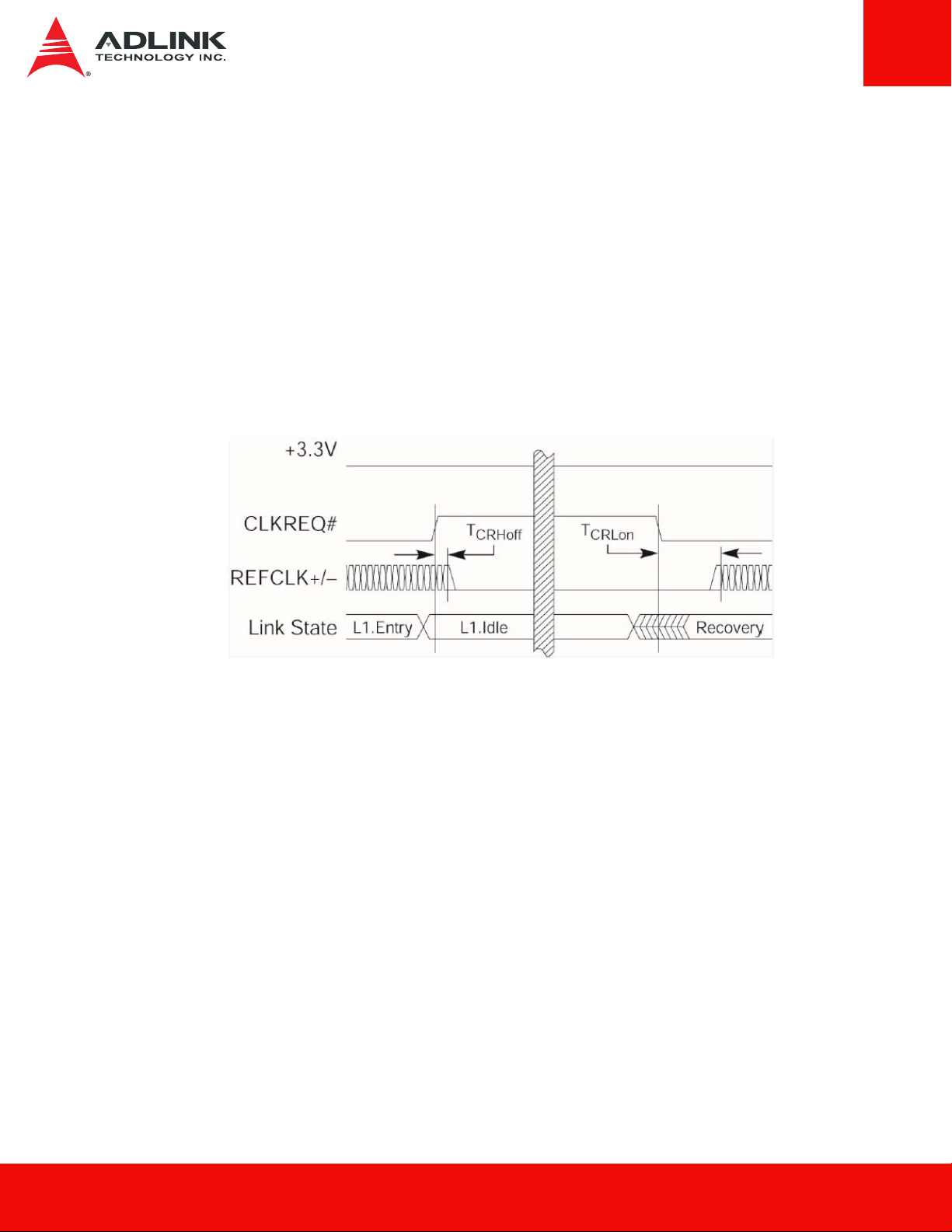
To exit L1, the device must assert CLKREQ# (low) to re-enable the reference clock. After the
device asserts CLKREQ# (low) it must allow that the reference clock will continue to be in the
parked clock state for a delay (TCRLon) before transitioning to the active clock state. The time
that it takes for the device to assert CLKREQ# and for the system to return the reference clock to
the active clock state are serialized with respect to the remainder of L1 recovery. This time must
be taken into account when the device is reporting its L1 exit latency.
When the PCI Express device supports, and is enabled for, Latency Tolerance Reporting (LTR),
the device must allow that the reference clock transition to the active clock state may be
additionally delayed by the system up to a maximum value consistent with requirements for the
LTR mechanism. During this delay, the reference clock must remain parked. When exiting the
parked state following the delay, the clock must be stable and valid within 400 ns.
Clock Request Support Reporting and Enabling
Support for the CLKREQ# dynamic clock protocol should be reported using bit 18 in the PCI
Express link capabilities register (offset 0C4h). To enable dynamic clock management, bit 8 of the
Link Control register (offset 010h) is provided. By default, the card shall enable CLKREQ#
dynamic clock protocol upon initial power up and in response to any warm reset by the host
system. System software may subsequently disable this feature as needed. Refer to the PCI
Express Base Specification, Revision 1. 1 (or later) for more information regarding these bits
PERST# Signal
• The PERST# signal is de-asserted to indicate when the system power sources are within
their specified voltage tolerance and are stable.
• PERST# should be used to initialize the card functions once power sources stabilize.
• PERST# is asserted when power is switched off and also can be used by the system to
force a hardware reset on the card.
• System may use PERST# to cause a warm reset of the add-in card.
Page 24 of 43 ASD8P-MT1 Specification
Page 25

Refer to the PCI Express Card Electromechanical Specification for more details on the functional
requirements for the PERST# signal.
WAKE# Signal
PCI Express M. 2 Cards must implement WAKE# if the card supports either the wakeup function
or the OBFF mechanism. Refer to the PCI Express Card Electromechanical Specification for more
details on the functional requirements for the WAKE# signal.
4.4 SDIO Interface
The M. 2 SDIO interface comprise of the following Standard SDIO signals:
• Four bi-directional Data signals, each capable of data rates up to 100Mbits/Sec (for a total of
400Mbits/Sec)
• One bi-directional CMD signal.
• One Clock signal up to 50MHz
These signals are in accordance to standard SDIO specifications. Refer to the SDIO Specification
for more details on the functional requirements for the SDIO interface signals.
• Electrical Specifications
• PCI Express M. 2 Specification | 99
• Revision 0. 7a, January 2, 2013
The M. 2 SDIO interface also includes two non-standard signals in support of new features related
to the SDIO interface. This includes the following signals:
• SDIO_Wake# The SDIO_Wake# signal is an output from the device (comms module) to the
platform used to trigger the wake the host and to initiate SDIO interface communication
between the device and the platform. This signal is an open drain output and needs to be
pulled high by the platform to 1. 8V always on.
• SDIO_RESET# The SDIO_RESET# signal is an input to the device from the platform and it is
used to reset the SDIO interface. The signal is 1. 8V at the module input.
Since the SDIO_RESET# and SDIO_WAKE# are not part of the standard SDIO specification, the
timing diagrams shown in Figure 80 and Figure 81 show their expected timing behavior. Table 20
lists the SDIO reset and power-up timing parameters.
ASD8P-MT1 Specification Page 25 of 43
Page 26

4.5 UART Interface
The on-chip asynchronous interface (UART, Universal Asynchronous Receiver and Transmitter)
can be used for communication with other host controllers or systems.
The UART can handle 8-bit data frames and inserts one start and one stop bit (with/without parity).
The format of the UART frame.
Page 26 of 43 ASD8P-MT1 Specification
Page 27

5 ATA Command Sets
5.1 ATA Command
The ASD8P-MT1 PCIe Gen2 x 2 Lane SSD supports all the mandatory ATA commands defined
in the ATA/ATAPI-8 specification.
ATA General Feature Command Set
The ASD8P-MT1 PCIe Gen2 x 2 Lane SSD supports the ATA General Feature Command set
(non-packet), which consists of
- EXECUTE DEVICE DIAGNOSTIC
- FLUSH CACHE
- IDENTIFY DEVICE
- READ DMA
- READ DMA WITHOUT RETRIES
- READ SECTOR(S)
- READ SECTORS(S) WITHOUT RETRIES
- READ VERIFY SECTORS(S)
- READ VERIFY SECTORS(S) WITHOUT RETRIES
- SEEK
- SET FEATURES
- WRITE DMA
- WRITE DMA WITHOUT RETRIES
- WRITE SECTOR(S)
- WRITE SECTOR(S) WITHOUT RETRY
- READ MULTIPLE
- SET MULTIPLE MODE
- WRITE MULTIPLE
- INITIALIZE DEVICE PARAMETERS
- DATA SET MANAGEMENT
The ASD8P-MT1 PCIe Gen2 x 2 Lane SSD supports all the following optional commands.
- READ BUFFER
- WRITE BUFFER
- DOWNLOAD MICROCODE
ASD8P-MT1 Specification Page 27 of 43
Page 28

Table 13 Supported ATA Command Set
Command Name
DATA SET MANAGEMENT 06h SET MULTIPLE MODE C6h
READ SECTOR(S) 20h READ DMA C8h
READ SECTOR(S) EXT 24h WRITE DMA CAh
READ DMA EXT 25h WRITE MULTIPLE FUA EXT CEh
READ NATIVE MAX ADDRESS EXT 27h STANDBY IMMEDIATE E0h
READ MULTIPLE EXT 29h IDLE IMMEDIATE E1h
READ LOG EXT 2Fh STANDBY E2h
WRITE SECTOR(S) 30h IDLE E3h
WRITE SECTOR(S) EXT 34h READ BUFFER E4h
WRITE DMA EXT 35h CHECK POWER MODE E5h
SET MAX ADDRESS EXT 37h SLEEP E6h
WRITE MULTIPLE EXT 39h FLUSH CACHE E7h
WRITE DMA FUA EXT 3Dh WRITE BUFFER E8h
WRITE LOG EXT 3Fh FLUSH CACHE EXT EAh
READ VERIFY SECTOR(S) 40h IDENTIFY DEVICE ECh
Command
Code
Command Name
Command
Code
READ VERIFY SECTOR(S) EXT 42h SET FEATURES EFh
READ FPDMA QUEUED 60h SECURITY SET PASSWORD F1h
WRITE FPDMA QUEUED 61h SECURITY UNLOCK F2h
EXECUTE DEVICE DIAGNOSTIC 90h SECURITY ERASE PREPARE F3h
DOWNLOAD MICROCODE 92h SECURITY ERASE UNIT F4h
SMART B0h SECURITY FREEZE LOCK F5h
DEVICE CONFIGURATION
OVERLAY
READ MULTIPLE C4h READ NATIVE MAX ADDRESS F8h
WRITE MULTIPLE C5h SET MAX ADDRESS F9h
B1h SECURITY DISABLE PASSWORD F6h
Page 28 of 43 ASD8P-MT1 Specification
Page 29

Identify Device Data
The following table details the sector data returned after issuing an IDENTIFY DEVICE command.
Table 14 Returned Sector Data
F=Fixed
Word
V=Variable
128GB 256GB 512GB
X=Both
0 F 0040h 0040h 0040h 0040h
1 F 3FFFh 3FFFh 3FFFh 3FFFh
2 F C837h C837h C837h C837h Specific configuration
3 F 0010h 0010h 0010h 0010h
4-5 F 0000h 0000h 0000h 0000h Retired
Default
Value
Description
General configuration bit-significant
information
Obsolete-Number of logical cylinders
(16,383)
Obsolete-Number of logical heads
(16)
6 F 003Fh 003Fh 003Fh 003Fh
7-8 F 0000h 0000h 0000h 0000h
9 F 0000h 0000h 0000h 0000h Retired
10-19 V Var. Var. Var. Var. Serial number (20 ASCII characters)
20-22 F 0000h 0000h 0000h 0000h Retired / Obsolete
23-26 V Var. Var. Var. Var.
27-46 V Var. Var. Var. Var. Model number
47 F 8010h 8010h 8010h 8010h
48 F 4000h 4000h 4000h 4000h
49 F 2F00h 2F00h 2F00h 2F00h Capabilities
50 F 4000h 4000h 4000h 4000h
51-52 F 0000h 0000h 0000h 0000h Obsolete
53 F 0007h 0007h 0007h 0007h Words 88 and 70: 64 valid
54 V Var. Var. Var. Var.
55 V Var. Var. Var. Var.
56 V Var. Var. Var. Var.
57-58 V Var. Var. Var. Var. Capacity(Cylinders*heads*sectors)
59 V 0101h 0101h 0101h 0101h
C2B0h FFFFh FFFFh
60-61 V
0EE7h 0FFFh 0FFFh
62 F 0000h 0000h 0000h 0000h Obsolete
Var by
capacity
Var by
capacity
Obsolete-Number of logical sectors
per logical track (63)
Reserved for assignment by the
Compact Flash Association
Firmware revision (8 ASCII
characters)
7: 0 – Maximum number of sectors
transferred per interrupt on multiple
commands
Trusted Computing feature set
options, bit14 should be 1
Trusted Computing feature set
options, bit14 should be 1
Obsolete . Number of logical cylinders
(16,383)
Obsolete . Number of logical heads
(16)
Obsolete . Number of logical sectors
per logical track (63)
Number of sectors transferred per
interrupt on multiple commands
Total number of user addressable
logical sectors for 28-bit commands
(DWord)
ASD8P-MT1 Specification Page 29 of 43
Page 30

F=Fixed
Word
V=Variable
128GB 256GB 512GB
X=Both
63 V 0007h 0007h 0007h 0007h
64 F 0003h 0003h 0003h 0003h PIO modes supported
65 F 0078h 0078h 0078h 0078h
66 F 0078h 0078h 0078h 0078h
67 F 0078h 0078h 0078h 0078h
68 F 0078h 0078h 0078h 0078h
69-70 F 0000h 0000h 0000h 0000h
71-74 F 0000h 0000h 0000h 0000h
75 F 001Fh 001Fh 001Fh 001Fh 4: 0 Maximum Queue depth-1=31
76 V 070Eh 070Eh 070Eh 070Eh Serial ATA capabilities
77 V Var. Var. Var. Var. Reserved for Serial ATA
78 V 004Ch 004Ch 004Ch 004Ch Serial ATA features supported
79 V 0040h 0040h 0040h 0040h Serial ATA features enabled
Default
Value
Description
Multi-word DMA modes
supported/selected
Minimum multiword DMA transfer
cycle time per word
Manufacture’s recommended
multiword DMA transfer cycle time
Minimum PIO transfer cycle time
without flow control
Minimum PIO transfer cycle time with
IORDY flow control
Reserved(for future command overlap
and queuing)
Reserved for the IDENTIFY packet
DEVICE command
80 F 01FEh 01FEh 01FEh 01FEh Major Version Number
81 F 0021h 0021h 0021h 0021h Minor Version Number
82 F 346Bh 346Bh 346Bh 346Bh
83 F 7D01h 7D01h 7D01h 7D01h
84 F 4023h 4023h 4023h 4023h
85 V 3469h 3469h 3469h 3469h
86 V BC01h BC01h BC01h BC01h
87 F 4023h 4023h 4023h 4023h
88 V 407Fh 407Fh 407Fh 407Fh Ultra DMA modes
89 F 0003h 0003h 0003h 0003h
90 F 0003h 0003h 0003h 0003h
91 F 0000h 0000h 0000h 0000h
92 V Var. Var. Var. Var. Master Password Identifier
93 V 0000h 0000h 0000h 0000h
94 F 0000h 0000h 0000h 0000h Current AAM value
Commands and feature sets
supported
Commands and feature sets
supported
Commands and feature sets
supported
Commands and feature sets
supported or enabled
Commands and feature sets
supported or enabled
Commands and feature sets
supported or enabled
Time required for security erase unit
completion
Time required for enhanced security
erase completion
Current advanced power
management value
Hardware reset result. The contents
of bits (12: 0) of this word shall
change only during the execution of a
hardware reset.
95 F 0000h 0000h 0000h 0000h Stream Minimum Request Size
Page 30 of 43 ASD8P-MT1 Specification
Page 31

F=Fixed
Word
V=Variable
128GB 256GB 512GB
X=Both
96 F 0000h 0000h 0000h 0000h Streaming Transfer Time . DMA
97 F 0000h 0000h 0000h 0000h
98-99 F 0000h 0000h 0000h 0000h Streaming Performance Granularity
100-
101
102-
103
104 F 0000h 0000h 0000h 0000h Streaming Transfer Time . PIO
105 F 0008h 0008h 0008h 0008h
106 F 4000h 4000h 4000h 4000h
107 F 0000h 0000h 0000h 0000h
108-
111
112-
115
116 F 0000h 0000h 0000h 0000h Reserved for TLC
117-
118
119 F 4010h 4010h 4010h 4010h
120 F 4010h 4010h 4010h 4010h
121-
126
127 F 0000h 0000h 0000h 0000h
128 V 0029h 0029h 0029h 0029h Security status
129-
159
160 F 0000h 0000h 0000h 0000h
161-
167
168 F 0000h 0000h 0000h 0000h
169 F 0001h 0001h 0001h 0001h
170-
173
174-
175
176-
205
206 F 003Dh 003Dh 003Dh 003Dh SCT Command Transport
207-
208
V
V 0000h 0000h 0000h
V Var. Var. Var. Var. World wide name
F 0000h 0000h 0000h 0000h
F 0000h 0000h 0000h 0000h Words per logical sector
F 0000h 0000h 0000h 0000h
F 0000h 0000h 0000h 0000h Vendor specific
F 0000h 0000h 0000h 0000h
V Var. Var. Var. Var.
F 0000h 0000h 0000h 0000h Reserved
F 0000h 0000h 0000h 0000h
F 0000h 0000h 0000h 0000h Reserved
C2B0h 32B0h 12B0h
0EE7h 1DCFh 3B9Eh
Default
Value
Var by
capacity
Var by
capacity
Description
Streaming Access Latency . DMA and
PIO
Maximum user LBA for 48-bit Address
feature set
Maximum number of 512-byte blocks
per DATA SET MANAGEMENT
command
Physical sector size/logical sector
size
Inter-seek delay for ISO-7779
acoustic testing in microseconds
Reserved for word wide name
extension to 128 bits
Commands and feature sets
supported
Commands and feature sets
supported or enabled
Reserved for expanded supported
and enabled settings
Removable Media Status Notification
feature set support
Compact Flash Association (CFA)
power mode 1
Reserved for the CompactFlash
Association
DATA SET MANAGEMENT
command is supported
Additional Product Identifier (ATA
String)
Current media serial number (ATA
string)
ASD8P-MT1 Specification Page 31 of 43
Page 32
F=Fixed
Word
V=Variable
128GB 256GB 512GB
X=Both
209 F 4000h 4000h 4000h 4000h
210-
211
212-
213
214 F 0000h 0000h 0000h 0000h NV Cache Capabilities
215-
216
217 F 0001h 0001h 0001h 0001h Nominal media rotation rate
218 F 0000h 0000h 0000h 0000h Reserved
219 F 0000h 0000h 0000h 0000h NV Cache Options
220 F 0000h 0000h 0000h 0000h
221 F 0000h 0000h 0000h 0000h Reserved
222 F 1075F 1075F 1075F 1075F Transport major version number
223 F 0000h 0000h 0000h 0000h Transport minor version number
224-
229
230-
233
234 F 0000h 0000h 0000h 0000h
235 F 0000h 0000h 0000h 0000h
236-
254
255 V Var. Var. Var. Var. Integrity word
F 0000h 0000h 0000h 0000h
F 0000h 0000h 0000h 0000h
F 0000h 0000h 0000h 0000h
F 0000h 0000h 0000h 0000h Reserved
F 0000h 0000h 0000h 0000h
F 0000h 0000h 0000h 0000h Reserved
Default
Value
Description
Alignment of logical blocks within a
physical block
Write-Read-Verify Sector Count Mode
3 (DWord)
Write-Read-Verify Sector Count Mode
2 (DWord)
NV Cache Size in Logical Blocks
(DWord)
7: 0 Write-Read-Verify feature set
current mode
Extended Number of User
Addressable Sectors (QWord)
Minimum number of 512-byte data
blocks per DOWNLOAD
MICROCODE command for mode
03h
Minimum number of 512-byte data
blocks per DOWNLOAD
MICROCODE command for mode
03h
Notes:
1. F=Fixed. The content of the word is fixed and does not change for removable media
devices, these values may change when media is Removed or changed.
2. V=Variable. The state of at least one bit in a word is variable and may change
depending on the state of the device or the commands executed by the device.
3. X=F or V. The content of the word may be fixed or variable.
Page 32 of 43 ASD8P-MT1 Specification
Page 33

5.2 Power Management Command Set
The ASD8P-MT1 PCIe Gen2 x 2 Lane SSD supports the power management command set, which
consists of
- CHECK POWER MODE
- IDLE
- IDLE IMMEDIATE
- SLEEP
- STANDBY
- STANDBY IMMEDIATE
5.3 Security Mode Feature Set
The ASD8P-MT1 PCIe Gen2 x 2 Lane SSD supports the Security Mode Feature Set,
which provide high reliability of data storage. Implementing personal password for disk drive to
prevent unauthorized access is available with this Security Mode Feature Set .
- SECURITY SET PASSWORD and SECURITY DISABLE PASSWORD
Manufacturer/dealer can set up new master password by using the command SECURITY
SET PASSWORD without locking function systematically or physically. Users can also set
up user password by the command. Once the user password is set, the drive will be locked
automatically and it will take effect by the next power on. The user password can be
disabled by SECURITY DISABLE PASSWORD command but the command can’t change
or disable the master password
- SECURITY UNLOCK
Any accessing media command to the locked drive will not be accepted until host
successfully receive and complete the SECURITY UNLOCK command,
- SECURITY ERASE PREPARE and SECURITY ERASE UNIT
Password loss problem can be solved under the conditions liste d below:
(A) Password is lost & High security level is set:
The data can’t be accessed without using master password to unlock the drive.
(B) Password is lost & Maximum security level is set:
It’s impossible to accessing data again. The drive can still be unlocked by executing
SECURITY ERASE PREPARE and SECURITY ERASE UNIT command, but all of the
data will be erased.
ASD8P-MT1 Specification Page 33 of 43
Page 34

- SECURITY FREEZE LOCK
The drive can be secured by executing SECURITY FREEZE LOCK command- After
command completion, the drive will be set to Frozen mode to prevents changes to all
Security states and any other commands to it will be aborted- The Frozen mode can be
disabled by power-off or rebooting-
5.4 SMART Command Set
The SMART command Set provides access to the Attribute Values, the Attribute Thresholds, and
other low level subcommands that can be used for logging and reporting purposes and to
accommodate special user needs- The SMART Feature Set command ha s several separate
commands which are selectable via the device's Features Register when the SMART Feature Set
command is issued by the host- To select a command, the host must write the subcommand code
to the device's Features Register before issuing the SMART Feature Set command-
The ASD8P-MT1 PCIe Gen2 x 2 Lane SSD supports the SMART command set, which consist of
- SMART ENABLE OPERATIONS
- SMART DISABLE OPERATIONS
- SMART ENABLE/DISABLE AUTOSAVE
- SMART RETURN STATUS
The ASD8P-MT1 PCIe Gen2 x 2 Lane SSD supports the following optional commands-
- SMART EXECUTE OFF-LINE IMMEDIATE
- SMART READ DATA
- SMART READ LOG
- SMART WRITE LOG
SMART ATTRIBUTE VALUES (READ DATA) (Code D0h)
This subcommand returns the device's Attribute Values to the host. Upon receipt of the SMART
Read Attribute Values subcommand from the host, the device asserts BSY, saves any updated
Attribute Values to the Attribute Data sectors, asserts DRQ, clears BSY, asserts INTRQ, and then
waits for the host to transfer the 512 bytes of Attribute Value information from the device via the
Data Register.
SMART READ ATTRIBUTE THRESHOLDS (Code D1h)
This subcommand returns the device's Attribute Thresholds to the host. Upon receipt of the
SMART Read Attribute Thresholds subcommand from the host, the device reads the Attribute
Page 34 of 43 ASD8P-MT1 Specification
Page 35

Thresholds from the Attribute Threshold sectors and then waits for the host to transfer the 512
bytes of Attribute Thresholds information from the device.
SMART ENABLE/DISABLE ATTRIBUTE AUTOSAVE (Code D2h)
This subcommand enables and disables the attribute auto save feature of the device. The
SMART Enable/Disable Attribute Autosave subcommand allows the device to automatically save
its updated Attribute Values to the Attribute Data Sector at the timing of the first transition to Active
idle mode and
after 15 minutes after the last saving of Attribute Values. This subcommand causes the auto save
feature to be disabled. The state of the Attribute Autosave feature—either enabled or disabled—
will be preserved by the device across the power cycle.
- A value of 00h—written by the host into the device's Sector Count Register before issuing
the SMART Enable/Disable Attribute Autosave subcommand—will cause this feature to be
disabled. Disabling this feature does not preclude the device from saving Attribute Values
to the Attribute Data sectors during some other normal operation such as during a power-up
or a power-down.
- A value of F1h—written by the host into the device's Sector Count Register before issuing
the SMART Enable/Disable Attribute Autosave subcommand—will cause this feature to be
enabled- Any other nonzero value written by the host into this register before issuing the
SMART Enable/Disable Attribute Autosave subcommand will not change the current
Autosave status.
The SMART Disable Operations subcommand disables the auto save feature along with the
device's SMART operations. Upon the receipt of the subcommand from the host, the device
asserts BSY, enables or disables the Autosave feature, clears BSY, and asserts INTRQ.
SMART SAVE ATTRIBUTE VALUES (Code D3h)
This subcommand causes the device to immediately save any updated Attribute Values to the
device's Attribute Data sector regardless of the state of the Attribute Autosave feature. Upon
receipt of the SMART Save Attribute Values subcommand from the host, the device asserts BSY,
writes any updated
Attribute Values to the Attribute Data sector, clears BSY, and asserts INTRQ.
SMART EXECUTE OFF-LINE IMMEDIATE (Code D4h)
This subcommand causes the device to immediately initiate the set of activities that collect
Attribute data in an offline mode (off-line routine) or execute a self-test routine in either captive or
off-line mode. The LBA Low register shall be set to specify the operation to be executed.
ASD8P-MT1 Specification Page 35 of 43
Page 36

SMART READ LOG SECTOR (Code D5h)
This command returns the indicated log sector contents to the host. Sector count sepcifies the
number of sectors to be read from the specified log. The log transfferred by the drive shall start at
the first sector in the speicified log, regardless of the sector count requested.
SMART READ LOG SECTOR (Code D6h)
This command writes 512 bytes of data to the specified log sector. The 512 bytes of data are
transferred at a command and the LBA Low value shall be set to one. The LBA Low shall be set
to specify the log sector address. If a Rea Only log sector is specified, the device returns ABRT
error.
SMART READ LOG SECTOR (Code D8h)
This subcommand enables access to all SMART capabilities within the device. Prior to receipt of
a SMART Enable Operations subcommand, Attribute Values are neither monitored nor saved by
the device. The state of SMART—either enabled or disabled—will be preserved by the device
across
power cycles. Once enabled, the receipt of subsequent SMART Enable Operations
subcommands will not affect any of the Attribute Values. Upon receipt of the SMART Enable
Operations subcommand from the host, the device asserts BSY, enables SMART capabilities and
functions, clears BSY, and asserts INTRQ.
SMART READ LOG SECTOR (Code D9h)
This subcommand disables all SMART capabilities within the device including the device's
attribute auto save feature. After receipt of this subcommand the device disables all SMART
operations. Non self-preserved Attribute Values will no longer be monitored. The state of
SMART—either enabled or disabled—is preserved by the device across power cycles. Note that
this subcommand does not preclude the device's power mode attribute auto saving.
Upon receipt of the SMART Disable Operations subcommand from the host, the device asserts
BSY, disables SMART capabilities and functions,clears BSY, and asserts INTRQ. After receipt of
the device of the SMART Disable Operations subcommand from the host, all other SMART
subcommands—with the exception of SMART Enable Operations—are disabled, and invalid and
will be aborted by the device—including the SMART
Any Attribute Values accumulated and saved to volatile memory prior to receipt of the SMART
Disable Operations command will be preserved in the device's Attribute Data Sectors. If the
device is re-enabled, these Attribute Values will be updated, as needed, upon receipt of a SMART
Read Attribute Values or a SMART Save Attribute Values command.
Page 36 of 43 ASD8P-MT1 Specification
Page 37

SMART READ LOG SECTOR (Code DAh)
This subcommand is used to communicate the reliability status of the device to the host's request.
Upon receipt of the SMART Return Status subcommand the device asserts BSY, saves any
updated Attribute Values to the reserved sector, and compares the updated Attribute Values to the
Attribute Thresholds.
If the device does not detect a Threshold Exceeded Condition, or detects a Threshold Exceeded
Condition but involving attributes are advisory, the device loads 4Fh into the LBA Mid register, C2h
into the LBA High register, clears BSY, and asserts INTRQ. If the device detects a Threshold
Exceeded Condition for prefailure attributes, the device loads F4h into the LBA Mid register, 2Ch
into the LBA High register, clears BSY, and asserts INTRQ. Advisory attributes never result in a
negative reliability condition.
SMART READ LOG SECTOR (Code DBh)
This subcommand enables and disables the optional feature that cause the device to perform the
set of off-line data collection activities that automatically collect attribute data in an off-line mode
and then save this data to the device's nonvolatile memory. It may either cause the device to
automatically initiate or resume performance of its off-line data collection activities or cause the
automatic off-line data collection feature to be disabled. It also enables and disables the off-line
read scanning feature that cause the device to perform the entire read scanning with defect
reallocation as the part of the off-line data collection activities.
Device's Sector Count of XXh written by the host before issuing SMART READ LOG SECTOR
command shall be set to specify the feature to be enabled or disabled:
- XXh = 00h: The automatic off-line data collection feature will be disabled- Disabling this
feature does not preclude the device from saving attribute values to nonvolatile memory
during some other normal operation such as during a power-on, during a power-off
sequence, or during an error recovery sequence.
- XXh = F8h: The automatic Off-line data collection feature will be enabled.
The table below lists the SMART commands.
Table 15 SMART commands
Subcommand Code LBA Low value
SMART ATTRIBUTE VALUES (READ DATA) D0h
READ ATTRIBUTE THRESHOLDS D1h
ENABLE/DISABLE ATTRIBUTE AUTOSAVE D2h
SAVE ATTRIBUTE VALUES D3h
ASD8P-MT1 Specification Page 37 of 43
Page 38

Subcommand Code LBA Low value
EXECUTE OFF-LINE IMMEDIATE D4h
EXECUTE SMART OFF-LINE ROUTINE
EXECUTE SMART SHORT SELF-TEST ROUTINE
(OFFLINE)
EXECUTE SMART EXTENDED SELF-TEST ROUTINE
(OFFLINE)
EXECUTE SMART SELECTIVE SELF-TEST ROUTINE
(OFFLINE)
ABORT OFF-LINE ROUTINE
EXECUTE SMART SHORT SELF-TEST ROUTINE
(CAPTIVE)
EXECUTE SMART EXTENDED SELF-TEST ROUTINE
(CAPTIVE)
EXECUTE SMART SELECTIVE SELF-TEST ROUTINE
(CAPTIVE)
READ LOG SECTOR D5h
WRITE LOG SECTOR D6h
ENABLE SMART OPERATIONS D8h
DISABLE SMART OPERATIONS D9h
00h
01h
02h
04h
7Fh
81h
82h
84h
RETURN SMART STATUS DAh
Enable/Disable Automatic OFFLINE DBh
5.5 Host Protected Area Command Set
The ASD8P-MT1 PCIe Gen2 x 2 Lane SSD supports the Host Protected Area command set which
consists of:
- READ NATIVE MAX ADDRESS
- SET MAX ADDRESS
- READ NATIVE MAX ADDRESS EXT
- SET MAX ADDRESS EXT
The ASD8P-MT1 PCIe Gen2 x 2 Lane SSD supports the following optional commands.
- SET MAX SET PASSWORD
- SET MAX LOCK
- SET MAX FREEZE LOCK
- SET MAX UNLOCK
Page 38 of 43 ASD8P-MT1 Specification
Page 39

5.6 48-Bit Address Command Set
The ASD8P-MT1 PCIe Gen2 x 2 Lane SSD supports the Host Protected Area command set,
which consists of:
- FLUSH CACHE EXT
- READ DMA EXT
- READ NATIVE MAX ADDRESS EXT
- READ SECTOR(S) EXT
- READ VERIFY SECTOR(S) EXT
- READ MULTIPLE EXT
- SET MAX ADDRESS EXT
- WRITE DMA EXT
- WRITE MULTIPLE EXT
- WRITE MULTIPLE FUA EXT
- WRITE SECTOR(S) EXT
5.7 Device Configuration Overlay Command Set
The ASD8P-MT1 PCIe Gen2 x 2 Lane SSD supports the Device configuration Overlay command
set, which consists of:
- DEVICE CONFIGURATION FREEZE LOCK
- DEVICE CONFIGURATION IDENTITY
- DEVICE CONFIGURATION RESTORE
- DEVICE CONFIGURATION SET
ASD8P-MT1 Specification Page 39 of 43
Page 40

6 SATA Command Sets
6.1 SATA Command
The SATA 3. 0 Specification is a super set of the ATA/ATAPI-8 specification with regard to
supported commands. The ASD8P-MT1 PCIe Gen2 x 2 Lane SSD also supports the following
features which are unique to the SATA 3. 0 Specification.
Software Settings Preservation
The ASD8P-MT1 PCIe Gen2 x 2 Lane SSD supports the SET FEATURES parameter to
enable/disable the preservation of software settings.
Native Command Queuing
The ASD8P-MT1 PCIe Gen2 x 2 Lane SSD supports the Native Command Queuing (NCQ)
command set, which includes.
- READ FPDMA QUEUED
- WRITE FPDMA QUEUED
Note: with a maximum queue depth equal to 32
Page 40 of 43 ASD8P-MT1 Specification
Page 41
7 References
This document references standards defined by a variety of organizations as listed below.
Table 16 Standards References
Date Title Location
Dec 2008 VCCI
July 2007 ROHS
July 2007 SFF-8144, 1. 8” drive form factor http: //www. sffcommittee. org
February
May 2006
2007
SFF-8223, 2. 5” Drive w/Serial Attachment
Serial ATA Revision 2. 6 http: //www. sata-io. org
Connector
http: //www. vcci. or.
jp/vcci_e/general/join/index. html
Search for material description
datasheet at http: //intel. pcnalert.
http: //www. sffcommittee. org
com
May 2005 SFF-8201, 2. 5” drive form factor http: //www. sffcommittee. org
April 2004 ATA-7 Spec. Volume 1 http: //www. t13. org/
Aug. 2009 ATA-8 Spec. Rev 2 http: //www. t13. org/
2008
2008
2004
2005
2008
2008
2004
International Electro Technical Commission
EB61000
4-2 Personnel Electrostatic Discharge
Immunity
4-3 Electromagnetic compatibility (EMC)
4-4 Electromagnetic compatibility (EMC)
4-5 Electromagnetic compatibility (EMC)
4-6Electromagnetic compatibility (EMC)
4-11 (Voltage variations)
ENV 50204 (Radiated electromagnetic field
from digital radio telephones)
http: //www. iec. ch
http: //www. iec. ch
ASD8P-MT1 Specification Page 41 of 43
Page 42

8 Getting Service
Contact us should you require any service or assistance.
ADLINK Technology, Inc.
Address: 9F , No.166 Jian Yi Roa d, Zhonghe District
New Taipei City 235, Taiwan
Tel: +886-2-8226-5877
Fax: +886-2-8226-5717
Email: service@adlinktech.com
Ampro ADLINK Technology, Inc.
Address: 5215 Hellyer Avenue, #110, San Jose, CA 95138, USA
Tel: +1-408-360-0200
Toll Free: +1-800-966-5200 (USA only)
Fax: +1-408-360-0222
Email: info@adlinktech.com
ADLINK Technology (China) Co., Ltd.
Address: 300 Fang Chun Rd., Zhangjiang Hi-Tech Park, Pudong New Area
Shanghai, 201203 China
Tel: +86-21-5132-8988
Fax: +86-21-5132-3588
Email: market@adlinktech.com
ADLINK Technology Beijing
Address: Rm. 801, Power Creative E, No. 1, B/D, Shang Di East Rd.
Beijing, 100085 China
Tel: +86-10-5885-8666
Fax: +86-10-5885-8625
Email: market@adlinktech.com
ADLINK Technology Shenzhen
Address: 2F, C Block, Bldg. A1, Cyber-Tech Zone, Gao Xin Ave. Sec. 7
High-Tech Industrial Park S., Shenzhen, 518054 China
Tel: +86-755-2643-4858
Fax: +86-755-2664-6353
Email: market@adlinktech.com
LiPPERT ADLINK Technology GmbH
Address: Hans-Thoma-Strasse 11, D-68163, Mannheim, Germany
Tel: +49-621-43214-0
Fax: +49-621 43214-30
Email: emea@adlinktech.com
ADLINK Technology, Inc. (French Liaison Office)
Address: 6 allée de Londres, Immeuble Ceylan
91940 Les Ulis, France
Tel: +33 (0) 1 60 12 35 66
Fax: +33 (0) 1 60 12 35 66
Email: france@adlinktech.com
Page 42 of 43 ASD8P-MT1 Specification
Page 43

ADLINK Technology Japan Corp oration
Address: KANDA374 Bldg. 4F, 3-7-4 Kanda Kajicho,
Chiyoda-ku, Tokyo 101-0045, Japan
Tel: +81-3-4455-3722
Fax: +81-3-5209-6013
Email: japan@adlinktech.com
ADLINK Technology, Inc. (Korean Liaison Office)
Address: 802, Mointer B/D, 326 Seocho-daero, Seocho-Gu,
Seoul 137-881, Korea
Tel: +82-2-2057-0565
Fax: +82-2-2057-0563
Email: korea@adlinktech.com
ADLINK Technology Singapore Pte. Ltd.
Address: 84 Genting Lane #07-02A, Cityneon Design Centre,
Singapore 349584
Tel: +65-6844-2261
Fax: +65-6844-2263
Email: singapore@adlinktech.com
ADLINK Technology Singapore Pte. Ltd. (Indian Liaison Office)
Address: #50-56, First Floor, Spearhead Towers
Margosa Main Road (between 16th/17th Cross)
Malleswaram, Bangalore .560 055, India
Tel: +91-80-65605817, +91-80-42246107
Fax: +91-80.23464606
Email: india@adlinktech.com
ADLINK Technology, Inc. (Israeli Liaison Office)
Address: 27 Maskit St., Corex Building
PO Box 12777
Herzliya 4673300, Israel
Tel: +972-77-208-0230
Fax: +972-77-208-0230
Email: israel@adlinktech.com
ADLINK Technology, Inc. (UK Liaison Office)
Tel: +44 774 010 59 65
Email: UK@adlinktech.com
ASD8P-MT1 Specification Page 43 of 43
 Loading...