

Page 1

Isolated Analog Output Card
NuDAQ®
ACL-6128A
2-CH 12-bit
User’s Guide
Page 2

Page 3

©Copyright 1995, 2003 ADLINK TECHNOLOGY INC.
All Rights Reserved.
Manual Rev. 1.00: August 12, 2003
Part No: 50-11032-100
The information in this document is subject to change without prior notice in
order to improve reliability, design and function and does not represent a
commitment on the part of the manufacturer.
In no event will the manufacturer be liable for direct, indirect, special, incidental,
or consequential damages arising out of the use or inability to use the product
or documentation, even if advised of the possibility of such damages.
This document contains proprietary information protected by copyright. All
rights are reserved. No part of this manual may be reproduced by any
mechanical, electronic, or other means in any form without prior written
permission of the manufacturer.
Trademarks
ACL-6128A is registered trademarks of ADLINK TECHNOLOGY INC.
Other product names mentioned herein are used for identification purposes
only and may be trademarks and/or registered trademarks of their respective
companies.
Page 4
Getting Service from ADLINK
Customer Satisfaction is top priority for ADLINK TECHNOLOGY INC. If you
need any help or service, please contact us.
ADLINK TECHNOLOGY INC.
Web Site http://www.adlinktech.com
Sales & Service Service@adlinktech.com
TEL +886-2-82265877 FAX +886-2-82265717
Address 9F, No. 166, Jian Yi Road, Chungho City, Taipei, 235 Taiwan
Please email or FAX your detailed information for prompt, satisfactory, and
consistent service.
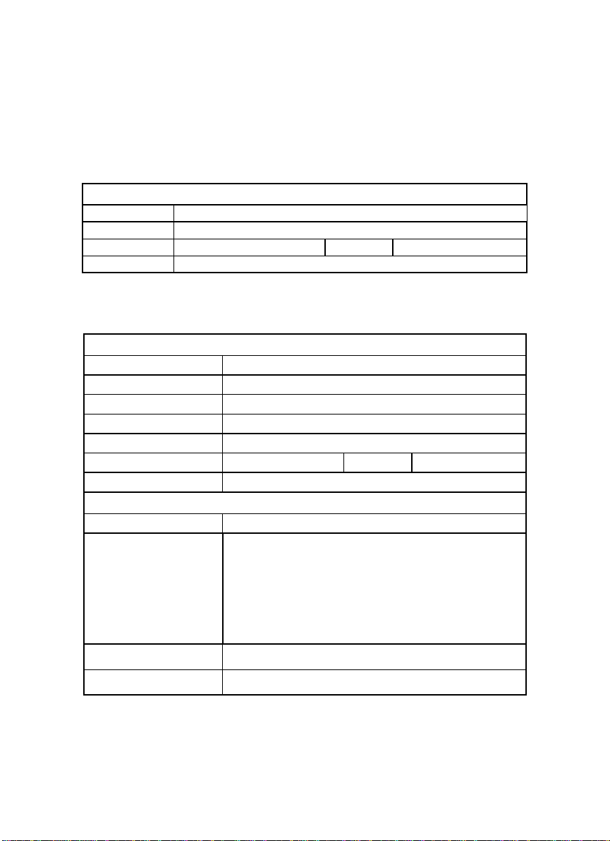
Detailed Company Information
Company/Organization
Contact Person
E-mail Address
Address
Country
TEL FAX
Web Site
Questions
Product Model
OS:
Computer Brand:
M/B: CPU:
Environment
Detail Description
Chipset: BIOS:
Video Card:
NIC:
Other:
Suggestions for ADLINK
Page 5

Table of Contents
Chapter 1 Introduction.......................................................1
1.1 Features................................................................................... 2
1.2 Applications.............................................................................. 2
1.3 Specifications........................................................................... 3
1.4 Software Support..................................................................... 4
1.4.1 Programming Library............................................................4
1.4.2 LabView Driver.....................................................................4
Chapter 2 Installation.........................................................5
2.1 What’s Included ....................................................................... 5
2.2 Unpacking................................................................................ 6
2.3 ACL-6128A's Layout................................................................ 7
2.4 Jumper and DIP Switch Description........................................ 7
2.5 Base Address Setting .............................................................. 8
2.6 Selecting D/A Range and Functions...................................... 10
2.6.1 Reference Source Setting……………………………………..10
2.6.2 Output Range Setting………………………………………….11
2.6.3 Summary………………………………………………………..13
2.7 Current Sink Range Setting................................................... 15
2.8 Connector Pin Assignment.................................................... 16
2.9 Signal Connection.................................................................. 17
2.9.1 Voltage Output Connection……………………………………17
2.9.2 Current Sink Connection………………………………………17
2.9.3 Floating Load without external power supply……………….18
Chapter 3 Low-Level Programming ................................ 19
3.1 I/O Port Address Map ............................................................ 19
3.2 D/A Data Format.................................................................... 20
3.3 Converted Data Representation............................................ 21
3.3.1 Unipolar Numbering……………………………………………21
3.3.2 Bipolar Numbering……………………………………………..21
3.4 D/A Conversion Sequence .................................................... 22
Chapter 4 High-Level Programming................................23
4.1 Installation.............................................................................. 24
4.3 C Language Library ............................................................... 25
Chapter 5 Calibration ....................................................... 27
Table of Contents • i
Page 6

5.1 What is Needed ..................................................................... 27
5.2 VR Assignment...................................................................... 28
5.3 Internal Reference Source Adjustment.................................. 28
5.4 Unipolar Output Calibration .................................................. 29
5.5 Bipolar Output Calibration..................................................... 30
5.6 Current Sink Calibration......................................................... 30
Warranty Policy.................................................................31
ii • Table of Contents
Page 7

How to Use This Guide
This manual is written to help users understand the ACL-6128A. Descriptions
of how to modify various settings on the ACL-6128A are provided in the
chapters below to meet your application specific requirements.
Chapter 1
Overview of product features, applications, and specifications.
Chapter 2
Installation instructions of the ACL-6128A with layout jumper
Chapter 3
Details register structure and programming for analog output in
Chapter 4
Describes programming for analog output using a high-level C
Chapter 5
Explains how calibration procedures for the ACL-6128A.
Introduction
Installation
settings, reference voltage source, D/A output ranges, pin
assignments, and signal connections.
Low-Level Programming
basic I/O primitive functions.
High-Level Programming
language library.
Calibration
How to Use This Guide • iii
Page 8

Page 9

1
Introduction
The ACL-6128A is an ideal cost effective analog output card with two separate
D/A converters In addition to 12-bit resolution and 16kHz throughput on each
DAC, supporting both voltage and current outputs for industrial applications.
The ACL-6128A provides high voltage isolation on each analog output channel.
Opto-isolators give 2500 V
from damage due to high voltages on the inputs. After powering on or resetting
the PC system, both channels will reset the output voltage to 0V in unipolar or
bioplar output range.
The ACL-6128A is fully compatible with the Advantech PCL-728, ensuring an
easy learning curve for customers familiar with Advantech products as well as
an easy replacement with addition functionality. Extra enhancements include
remarkable reliability and performance, surface mount components design, and
single +5V power consumption.
isolation to protect both the PC and peripherals
RMS
Introduction • 1
Page 10

1.1 Features
The ACL-6128A 2-channel Isolated D/A Card provides the following advanced
features:
• Fully compatible with ADLINK ACL-6128 and AdvantechPCL-728
• Two independent 12-bit analog output channels
• 2500 V
• 12-bit resolution, multiplying D/A converter
• Multiple output ranges
• Bipolar: ±10V, ±5V
• Unipolar: 0-10V, 0-5V
• Sink: 0-20mA, 4-20mA current loop
• Integral DC-to-DC converter for stable output operations
• Compact, half-size PCB
• 4-layer PCB with an integral ground plane
Isolation (channel-to-channel, input-to-output)
RMS
1.2 Applications
• Arbitrary waveform generation
• Control of values, switches, relays
• Programmable voltage source
• Servo Control
• Programmable current sink
2 • Introduction
Page 11

1.3 Specifications
The ACL-6128A provides the following specifications:
Analog Output (D/A)
♦
Output Channel:
•
Resolution:
•
Settling Time:
•
Output Range:
•
Bipolar Voltage:
•
Unipolar Voltage:
•
Current Loop (sink) :
•
Reference voltages
•
Internal:
External:
Output Drive Current:
•
Current Loop Excitation Voltage:
•
20mA.
Isolation Voltage:
•
Accuracy:
•
Linearity:
•
Data Transfer:
•
Temperature coefficient
•
2 Isolated channels
12-bit, multiplying D/A converter
≤ 30 μs
(Jumper selectable)
±10V, ±5V
0-10V, 0-5V
0-20mA, 4-20mA
-5V and -10V
DC or AC, ± 10V (max.)
5mA
±
+8V min, 36V max for 0-20mA or 4-
2500V
RMS
±0.012% of FSR
1/2 LSB
±
Programmable I/O
5ppm typical, 15ppm maximum
General Specifications
♦
Bus Type:
•
Connector:
•
Operating Temperature:
•
Storage Temperature:
•
Humidity:
•
Power Consumption:
•
Dimension:
•
PC/AT Bus
Two 9-pin D-sub female connector
5 - 95%, non-condensing
0°C - 55°C
-20°C - 70°C
+5V @ 780mA typical, 1A max
163 mm (L) x 107 mm (M)
Introduction • 3
Page 12

1.4 Software Support
1.4.1 Programming Library
A MS-DOS Borland C/C++ programming library is included for customers
writing application specific programs,
ACLS-DLL2 is a Development Kit for NuDAQ ISA bus cards with analog I/O for
Windows 3.1/9x/NT/2000. ACLS-DLL2 can be used with most programming
environments, such as Visual C++, Visual Basic, and Delphi. ACLS-DLL2 is
included in the ADLINK CD and requires a license.
1.4.2 LabView Driver
The ACLS-LVIEW LabView driver includes the ACL-6128A VIs to interface with
LabView. ACLS-LVIEW supports Windows 9x/NT/2000/XP. ACLS-LVIEW is
included in the ADLINK CD and requires a license.
4 • Introduction
Page 13

2
Installation
This chapter describes how to unpack and install the ACL-6128A. Package
contents and unpacking information should be careful reviewed. Jumper and
switch settings for the ACL-6128A's base address, reference voltage sources,
and output voltage range are also specified.
2.1 What’s Included
In addition to this User's Manual, the package includes:
• ACL-6128A 2-channel Isolated Analog Output Card
• ADLINK CD
If the card is missing or damaged, contact an ADLINK dealer. Save the
shipping materials and carton to ship or store the product in the future.
Installation • 5
Page 14

2.2 Unpacking
The ACL-6128A card contains sensitive electronic components that can be
easily damaged by static electricity.
Prepare a grounded anti-static mat. The operator should be wearing an antistatic wristband, grounded at the same point as the anti-static mat.
Inspect the card module carton for obvious damage. Shipping and handling
may cause damage to the module. Be sure there is no obvious damage due to
shipping and handing by examining the shipping box.
After opening the card module carton, extract the system module and place it
only on a grounded anti-static surface, component side up.
Again inspecting the module for damage. Press down on all the docketed IC's
to make sure they are properly seated. Do this only with the module place on a
firm flat surface.
Note:
DO NOT APPLY POWER TO THE CARD IF IT HAS BEEN
DAMAGED.
You are now ready to install your ACL-6128A.
6 • Installation
Page 15

2.3 ACL-6128A's Layout
VR5V
JP1 JP2
SW1
JP7
JP8
VR7 VR8
TB2
VR9
JP9
VR10
JP10
VR11
VR12
CN2
Figure 2.1 ACL-6128A‘s Layout
JP3
JP4
TB1
VR3
JP6
VR1
VR2
VR4
R6
6128A Isolated 2CH D/A ACRD
JP5
CN1
2.4 Jumper and DIP Switch Description
You can change the ACL-6128A's channels and base address by setting
jumpers and DIP switches on the card. The card's jumpers and switches are
preset at the factory. Under normal circumstances, these settings should not
need to be changed.
A jumper switch is closed or "shorted" with the plastic cap inserted over two
pins of the jumper. A jumper is open when the plastic cap inserted over one or
no pin(s) of the jumper.
Installation • 7
Page 16

2.5 Base Address Setting
The ACL-6128A requires 16 consecutive address locations in I/O address
space. The base address of the ACL-6128A is restricted by the following
conditions:
1.
The base address must be within the range 200hex to 3F0hex.
2.
The base address should not conflict with any PC reserved I/O address
(see Appendix A).
The ACL-6128A I/O port base address is selectable by an 8 position DIP switch
SW1 (refer to Figure 2.1). The address setting for the I/O port is from Hex 200
to Hex 3F0 is described in Table 2.1 below. The default base address (Hex
2C0) of the is illustrated in the Figure 2.2 below.
SW1 : Base Address = 2C0H
ON DIP
X
1 2 3 4 5 6 7
8
A ( 9 8 7 6 5 4 3 X )
Figure 2.2 Default Base Address Setting
I/O port
address(hex) 1 A9 2 A8 3 A7 4 A6 5 A5 6 A4 7 A3 8 X
200-20F
210-21F
:
(*) 2C0-2CF
:
300-30F
:
3F0-3FF
8 • Installation
OFF
OFF
OFF
OFF
OFF
(1)
ON
ON
ON
ON
(1)
(0)
(0)
(0)
(1)
(0)
(0)
ON
(0)
OFF
(1)
ON
(0)
OFF
(1)
OFF
(1)
ON
(0)
ON
(0)
(1)
ON
OFF
ON
OFF
(1)
(1)
(1)
OFF
(1)
OFF
(1)
(0)
ON
(0)
ON
(0)
ON
(0)
ON
(0)
OFF
(1)
ON
(0)
ON
(0)
OFF
(1)
Table 2.1
ON
(0)
ON
(0)
ON
(0)
ON
(0)
ON
(0)
X
X
X
X
X
Page 17

(*) : default setting ON : 0
X : don't care OFF : 1
Note : A3-A9 correspond to PC bus address lines.
How to Define a Base Address for the ACL-6128A ?
DIP1 to DIP7 in switch SW1 are one-to-one corresponding to the PC bus
address lines A9 through A3. A0, A1, and A2 are always 0. To change
the base address, change the values of A9 to A3 (shadow area of below
diagram). The following table shows how to define the base address as
Hex 2C0.
Base Address : Hex 2C0
2 C 0
1 0 1 1 0 0 0 0 0 0
A9 A8 A7 A6 A5 A4 A3 A2 A1 A0
Installation • 9
Page 18
2.6 Selecting D/A Range and Functions
There are two factors will effect the output voltage of ACL-6128A: reference
source and output range
2.6.1 Reference Source Setting
The ACL-6128A D/A converter reference voltage source can be internally
generated or an external reference voltage from the Reference Voltage Input
(REF.IN) of connectors CN1 and CN2. The settings of the reference sources
for CH1 and CH2 are controlled by jumpers JP4 and JP8, respectively. The
default setting is Internal Reference for both CH1 and CH2, and is illustrated
below.
CH1
CH2
.
Internal Reference
( Default )
JP4
EXT
INT
JP8
EXT
INT
External Reference
Voltage
JP4
EXT
INT
JP8
EXT
INT
Figure 2.3 Reference Source Setting
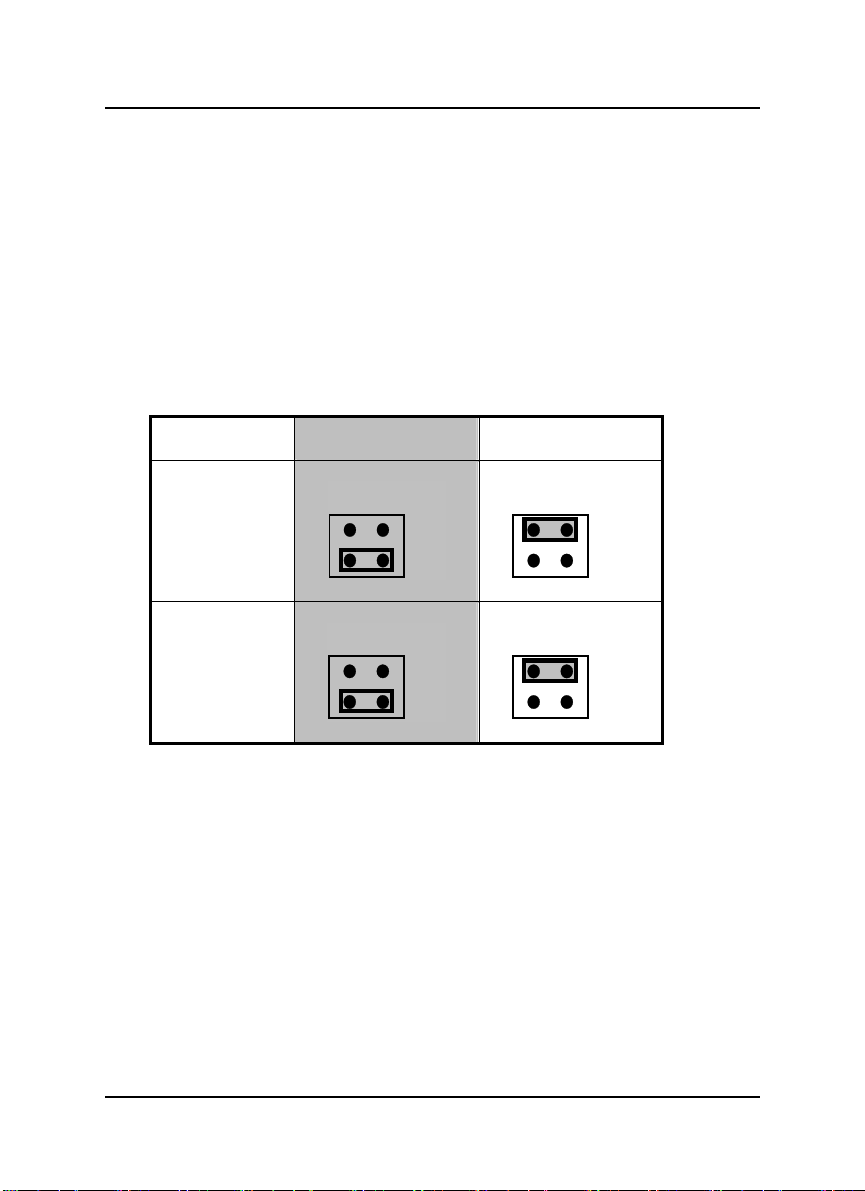
After setting as internal reference source, two fixed precision internal -5V and 10V reference sources are provided by ACL-6128A. The source selection is set
by JP3 (CH1) and JP7 (CH2), and the default setting of internal reference
voltage is -5V, which is illustrated as Figure 2.4 below:
10 • Installation
Page 19

Channel No.
CH1
CH2
Figure 2.4 Internal Reference Voltage Setting
If users choose the external reference, both AC and DC voltage sources can
be used by the external reference. The maximum input voltage is +/- 10V. The
voltage sources can be input through Pin 3 of the CN1 and CN2 connectors.
Internal -5V
( Default)
JP3
-10
-5
JP7
-10
-5
Internal -10V
JP3
-10
-5
JP7
-10
-5
2.6.2 Output Range Setting
The output voltage range of ACL-6128A can be set either Bipolar or Unipolar.
The jumpers, JP1 and JP5 (for CH1), and JP2 and JP9 (for CH2) are used for
the settings as illustrated in Figure 2.5 below (ACL-6128A and ACL-6128
respectively):
ACL-6128A settings (
Jumper settings for the older ACL-6128 are slightly different—see below.)
Channel No.
CH1
CH2
Note
: These settings are for the
Unipolar
( Default )
JP1 JP5
BP
UP
JP2 JP9
BP
UP
UP
BP
UP
BP
ACL-6128A
Bipolar
JP1 JP5
BP
UP
JP2 JP9
BP
UP
UP
BP
UP
BP
Installation • 11
only.
Page 20

ACL-6128 settings (
Jumper settings for the newer ACL-6128 are slightly different—see above. Also,
JP9 on the PCB of the older
and “UP” is the bottom pin.)
Channel No.
CH1
CH2
Note
: These settings are for the older
ACL-6128 ONLY
Unipolar
( Default )
JP1 JP5
BP
UP
JP2 JP9
BP
UP
Figure 2.5 Output Range Setting
is mislabeled. “BP” is the top pin
BP
UP
UP
BP
UP
UP
JP1 JP5
JP2 JP9
ACL-6128
Bipolar
BP
BP
BP
UP
BP
UP
only.
12 • Installation
Page 21

2.6.3 Summary
J
J
Users can configure the output voltage of CH1 and CH2 for application specific
needs according to the reference source and output range settings. can follow
the below table to. Settings are listed in two separate tables for the ACL-6128A
and ACL-6128, respectively.
(JP1, JP3, and JP5 are for CH1. JP2, JP7, and JP9 are for CH2)
ACL-6128A settings (Note: this table is for the ACL-6128A ONLY.)
Jumper
Output Range
0 to +5V
Unipolar
(Default)
0V to +10V
Unipolar
-5V to +5V
Bipolar
-10V to +10V
Bipolar
JP3 for CH1
JP7 for CH2
P3/JP7
P3/JP7
JP3/JP7
P3/JP7
-10
-5
-10
-5
-10
-5
-10
-5
JP1 & JP5 for CH1
JP2 & JP9 for CH2
JP1/JP2 JP5/JP9
BP
UP
JP1/JP2 JP5/JP9
BP
UP
JP1/JP2 JP5/JP9
BP
UP
JP1/JP2 JP5/JP9
BP
UP
UP
BP
UP
BP
UP
BP
UP
BP
Installation • 13
Page 22

ACL-6128 settings (Note: this table is for the older ACL-6128 ONLY. The
ACL-6128 PCB has misprints. Please refer to the chart below for correct
jumper placement.)
Jumper
Output Range
0 to +5V
Unipolar
(Default)
0V to +10V
Unipolar
-5V to +5V
Bipolar
-10V to +10V
Bipolar
JP3 for CH1
JP7 for CH2
P3/JP7
P3/JP7
JP3/JP7
P3/JP7
-10
-5
-10
-5
-10
-5
-10
-5
JP1 & JP5 for CH1
JP2 & JP9 for CH2
JP1/JP2 JP5/JP9
BP
UP
JP1/JP2 JP5/JP9
BP
UP
JP1/JP2 JP5/JP9
BP
UP
JP1/JP2
BP
UP
BP
UP
BP
UP
BP
UP
JP5/JP9
BP
UP
14 • Installation
Figure 2.6 Output Range Summary
Page 23

2.7 Current Sink Range Setting
In addition to voltage output, the ACL-6128A also provides either 0-20mA
or 4-20mA current sink. In order to use the current sink range, set the
output voltage to unipolar. Jumper JP6 corresponds to CH1 and JP10 is
used with CH2. Figure 2.7 shows the settings for the ACL-6128A current
sink range.
Channel No.
CH1
4-20mA
( Default )
JP6
0
0-20mA
0
JP6
CH2
Note :
The current sink can
internal reference with -5V
as
4
JP10
0
4
Figure 2.7 Current Sink Setting
ONLY
be used when the output voltage range set
and
4
JP10
0
4
unipolar mode.
Installation • 15
Page 24

2.8 Connector Pin Assignment
The ACL-6128A is equipped with two D-9 female connectors: CN1 and CN2.
Both CN1 and CN2 are located on the rear plate. CN1 and CN2 are the
outputs of CH1 and CH2, respectively. Each connector's pin assignment is
specified as follows:
Legend : V.OUT : Analog Voltage Output
I.SINK : Current Sink
A.GND : Analog Ground
REF.IN : Reference Voltage Input
+15V : +15V output
CN 1: Analog Output for Channel 1
♦
1
V.OUT
A.GND
REF.IN
A.GND
A.GND
CN2 : Analog Output for Channel 2
♦
2
3
4
5
1
V.OUT
A.GND
REF.IN
A.GND
A.GND
2
3
4
5
6
7
8
9
6
7
8
9
A.GND
I.SINK
A.GND
+15V
A.GND
I.SINK
A.GND
+15V
16 • Installation
Page 25

2.9 Signal Connection
A correct signal connection is vital to send data accuracy. This section
illustrates proper signal connection when the ACL-6128A is used.
2.9.1 Voltage Output Connection
ACL-6128A Side
Externa
Side
Rload
-
Amp
2.9.2 Current Sink Connection
ACL-6128A Side
ACL- 6128 Side
I.SINK
Amp
V.OU
A.GND
External
Side
Power
Supply
+
Load
A.GND
Rload
Note : For 4-20mA current sink mode, the output range should be set as
Internal Reference with -5V and Unipolar mode.
Installation • 17
Page 26

r
2.9.3 Floating Load without external power supply
The ACL-6128A provides a +15V power source for systems that do not offer
external power supplies. The connection is as follows:
D/A
Converte
ACL- 6128A Side
Amp
A.GND
+15V
I.SINK
External
Side
Load
18 • Installation
Page 27

3
Low-Level Programming
This chapter describes low-level programming of the ACL-6128A and details
the register format and control procedures. To write applications based on
primitive I/O functions (inportb and outportb) instead of using the ACL-6128A
library, be careful to fully understand the register structure.
3.1 I/O Port Address Map
The ACL-6128A requires only 4 consecutive addresses in the PC I/O address
space. The following table (Table 3.1) shows the location of each register and
driver relative to the base address.
Location Write Read
Base + 0 CH1 High Byte Data Not Used
Base + 1 CH1 Low Byte Data Not Used
Base + 2 CH2 High Byte Data Not Used
Base + 3 CH2 Low Byte Data Not Used
Table 3.1 I/O Register Map
Low-Level Programming • 19
Page 28

3.2 D/A Data Format
The base address from Base+0 to Base+3 is used for D/A conversion. The
analog output channels and its corresponding registers are specified by table
3.2.
CH NO. CHANNEL 1 CHANNEL 2
High byte Base+0 Base+2
Low byte Base+1 Base+3
Table 3.2
Address : BASE + 0 & BASE + 1
Attribute:
Data Format : (for D/A Channel 1)
Address : BASE + 2 & BASE + 3
Attribute:
Data Format: (for D/A Channel 2)
DA11 .. DA0:
DA0
X:
Don't care.
write only
Bit 7 6 5 4 3 2 1 0
Base + 0 X X X X DA11 DA10 DA9 DA8
Base + 1 DA7 DA6 DA5 DA4 DA3 DA2 DA1 DA0
write only
Bit 7 6 5 4 3 2 1 0
Base + 2 X X X X DA11 DA10 DA9 DA8
Base + 3 DA7 DA6 DA5 DA4 DA3 DA2 DA1 DA0
Digital to Analog data.
is the Least Significant Bit, and
DA11
is the Most Significant Bit.
20 • Low-Level Programming
Page 29

3.3 Converted Data Representation
Two analog output range alternatives are provided by the ACL-6128A: Unipolar
and Bipolar. The numbering of the converted data with have different
presentations for different output ranges.
3.3.1 Unipolar Numbering
0 40952048
0000 0000 0000 1000 0000 0000 1111 1111 1111
V.OUT=-Vref*(0/4095) V.OUT=-Vref*(2048/4095) V.OUT=-Vref*(4095/4095)
Example:
Converted Data =2047
Binary Code =0111 1111 1111
Vref =-5V
V.OUT =-(-5 V) * ( 2047/4095) = 2.499 V
3.3.2 Bipolar Numbering
-2048
0000 0000 0000
V.OUT=-Vref*(-2048/2047)
1000 0000 0000
V.OUT=-Vref*(0/2047)
= 0V
Example:
Converted Data =500
Binary Code =1001 1111 0100
Vref =-5V
V.OUT =-(-5 V) * ( 500/2047) = 1.221 V
Low-Level Programming • 21
20470
1111 1111 1111
V.OUT=-Vref*(2047/2047)
Page 30

3.4 D/A Conversion Sequence
In the ACL-6128A, the A/D conversion can only be controlled by software using
the double buffering concept. That is, the converted data should be stored in
High Byte Register first, and then stored the Low Byte Register.
The procedure of how to initiate and convert digital data to analog output is
listed below:
1. Define the base address of the ACL-6128A card:
Base_Addr = 0x2C0;
2. Extract the most signification 4 bits from the converted data then write
to Base_Addr + 0:
High_Byte = Data & 0f00;
outportb( Base_Addr + 0, High_Byte);
3. Extract the least signification 8 bits from the converted data then write
to Base_Addr + 1:
Low_Byte = Data & 00ff;
outportb( Base_Addr + 1, Low_Byte);
An example program in low-level programming style called
included in the Utility and Software Library CD for your reference.
6128IO.C
is
22 • Low-Level Programming
Page 31

4
High-Level Programming
A high-level C language programming interface for the ACL-6128A is described
in this chapter. Use the C library to easily and quickly develop customized
applications.
Only three C-language functions are supported by the software library. The
functionality of these function calls can be classified into the following
capabilities:
1. Initialization:
2. D/A conversion:
In addition to the library, some sample programs are also provided. Refer to
them to save programming time.
Initializes the hardware base I/O address and switches
between cards.
performs digital to analog conversion.
High-Level Programming • 23
Page 32

4.1 Installation
To install the DOS library software and utilities, please follow the following
installation procedures:
1. Put the ADLINK CD into an appropriate CD-ROM drive.
2. Type the following commands to change to the card’s directory (
indicates the CD-ROM drive):
X:\>CD \NuDAQISA\6128
3. Execute the setup batch program to install the software:
X:\NuDAQISA\6128>SETUP
After installation, all the files for the ACL-6128A Library & Utility for DOS are
stored in the
C:\ADLINK\6128\DOS
directory.
X
24 • High-level Programming
Page 33

4.3 C Language Library
The ACL-6128A digital-to-analog conversion library was constructed to provide
a simple programming interface for communicating with the ACL-6128A card.
The library provides easy to use functions which allow programmers to use the
features of the card in a high-level way.
The version of this library included in the CD is DOS only.
The detailed function description is specified in the following sections:
4.3.1 _6128_Initial
@ Description
An ACL-6128A card is initialized according to the card number and its
corresponding base address. Every ACL-6128A has to be initialized by this
function before calling other functions.
@ Syntax
int _6128_Initial(int card_number, int base_address)
@ Argument
card_number: The card number to be initialized, up to
base_address: The I/O port base address of the card.
@ Return Code
ERR_NoError
ERR_InvalidBoardNumber
ERR_BaseAddressError
8 cards can be initialized, the card
number must be within the range of 0 and
7.
High-Level Programming • 25
Page 34

4.3.2 _6128_Switch_Card_No
@ Description
This function is used on multi-cards systems. After the ACL-6128A cards
are initialized by the _6128_Initial function, you can use this function
to select which card to operate.
@ Syntax
int _6128_Switch_Card_No(int card_number)
@ Argument
card_number: The card number to be initialized, up to
@ Return Code
ERR_NoError
ERR_InvalidBoardNumber
8 cards can be initialized, the card
number must be within the range of 0 and
7.
4.3.3 _6128_DA
@ Description
This function is used to write data to D/A converters. There are two Digitalto-Analog conversion channel in the ACL-6128A. The resolution of each
channel is 12 bits, providing a range from 0 to 4095.
@ Syntax
int _6128_DA( int da_ch_no, unsigned int da_data )
@ Argument
da_ch_no : The DA channel number, the value has to
da_data : D/A converted value, if the value is
@ Return Code
ERR_NoError
ERR_BoardNoInit
ERR_InvalidDAChannel
be set a 0 or 1.
greater than 4095, the upper 4 bits are
negligent.
26 • High-level Programming
Page 35

5
Calibration
In data acquisition process, how to calibrate your measurement devices to
maintain its accuracy is very important. This chapter will guide you to calibrate
your ACL-6128A to an accurate condition.
5.1 What is Needed
Before calibrating the ACL-6128A card, please prepare the following:
1.
Calibration program: executing this program will walk users through the
calibration steps. The calibration program is located in the
C:\ADLINK\6128\dos\driver\util\6128av.exe
2.
Digital multimeter.
directory:
Calibration • 27
Page 36

5.2 VR Assignment
There are twelve variable resistors (VR) on the ACL-6128A board to allow
users to make accurate adjustment on two D/A channels. VR1 to VR6 belong
to CH1, and VR7 to VR12 belongs to CH2. The detailed functionality of each
VR is listed below:
CH1‘s VR
(-10V) Internal reference
VR1
Gain Adjustment
VR3
Current Sink Offset (4mA)
VR5
CH2‘s VR
(-10V) Internal reference
VR7
Gain Adjustment
VR9
Current Sink Offset (4mA)
VR11
There are two testing points (TP1 and TP2) on the board, which are used for
calibration the ACL-6128A. TP1 is for CH1, and TP2 is for CH2.
(-5V) Internal reference
VR2
Unipolar Offset
VR4
Bipolar Offset
VR6
(-5V) Internal reference
VR8
Unipolar Offset
VR10
Bipolar Offset
VR12
5.3 Internal Reference Source Adjustment
The Internal Reference Source adjustment can ensure that the internal
reference voltages of the ACL-6128A can offer very accurate voltage source—5V and -10V.
1.
Ground the black probe of the voltmeter.
2.
Connect the other probe to TP1 (for testing CH1), or TP2 (for testing
CH2).
Change the jumper to JP3 (for CH1) or JP7 (for CH2), trim
CH1) until the voltmeter reads
voltmeter also reads
3.
Change the jumper to JP3 (for CH1) or JP7 (for CH2), trim
CH1) until the voltmeter reads
voltmeter also reads
-10V
-5V
.
.
-10V
-5V
, trim
, trim
VR7
VR8
(for CH2) until the
(for CH2) until the
VR1
VR2
(for
(for
28 • Calibration
Page 37

5.4 Unipolar Output Calibration
If you choose Unipolar mode for analog output, you have to go through the
Unipolar Output Calibration. There are two steps: Gain Calibration and Offset
Calibration.
Gain Calibration:
1.
Set jumpers JP1 and JP5 (for CH1) or JP2 and JP9 (for CH2) to
unipolar,
2.
Set the digital data as (0000 0000 0000)B, trim VR4 (for CH1) or VR10
(for CH2) until the voltmeter reading is
Offset Calibration:
1.
Set jumpers JP1 and JP5 (for CH1) or JP2 and JP9 (for CH2) to
unipolar
2.
Set the digital data as (1111 1111 1111)B, trim VR3 (for CH1) or VR9
(for CH2) until the voltmeter reading is
and choose an internal reference as
0V
, and choose an internal reference as
5V
-5V
.
.
-5V
.
.
Calibration • 29
Page 38

5.5 Bipolar Output Calibration
If Bipolar mode for analog output is used, use Bipolar Output Calibration to
correctly calibrate. There are two steps involved: Gain Calibration and Offset
Calibration.
Gain Calibration:
1.
Set jumpers
bipolar, and choose an internal reference as
2.
Set the digital data as (1000 0000 0000)B, trim VR4 (for CH1) or VR10
(for CH2) until the voltmeter reading is
Offset Calibration:
1.
Set the internal reference to -5V.
2.
Set the digital data as (0000 0000 0000)B, trim VR6 (for CH1) or VR12
(for CH2) until the voltmeter reading is
JP1
and
JP5
(for
CH1
) or
0V
-5V
.
.
JP2
-5V
and
.
JP9
5.6 Current Sink Calibration
If using current sink output, please do the following:
Use
Follow the below procedures to calibrate the current sink output.
-5V
for internal reference and its reference voltage.
1.
Set the digital data as (0000 0000 0000)B, and internal reference as
5V
, using unipolar output range.
2.
Tr im VR5 (for CH1) or VR11 (for CH2) until there is a constant current
4mA
of
.
(for
CH2
) as
-
30 • Calibration
Page 39

Warranty Policy
Thank you for choosing ADLINK. To understand your rights and enjoy all the
after-sales services we offer, please read the following carefully.
1. Before using ADLINK’s products please read the user manual and follow
the instructions exactly. When sending in damaged products for repair,
please attach an RMA application form which can be downloaded from:
http://rma.adlinktech.com/policy/.
2. All ADLINK products come with a limited two-year warranty, one year for
products bought in China.
• The warranty period starts on the day the product is shipped from
ADLINK’s factory.
• Peripherals and third-party products not manufactured by ADLINK
will be covered by the original manufacturers' warranty.
• For products containing storage devices (hard drives, flash cards,
etc.), please back up your data before sending them for repair.
ADLINK is not responsible for any loss of data.
• Please ensure the use of properly licensed software with our
systems. ADLINK does not condone the use of pirated software and
will not service systems using such software. ADLINK will not be
held legally responsible for products shipped with unlicensed
software installed by the user.
• For general repairs, please do not include peripheral accessories. If
peripherals need to be included, be certain to specify which items
you sent on the RMA Request & Confirmation Form. ADLINK is not
responsible for items not listed on the RMA Request & Confirmation
Form.
3. Our repair service is not covered by ADLINK's guarantee in the following
situations:
• Damage caused by not following instructions in the User's Manual.
• Damage caused by carelessness on the user's part during product
transportation.
• Damage caused by fire, earthquakes, floods, lightening, pollution,
other acts of God, and/or incorrect usage of voltage transformers.
Warranty Policy • 31
Page 40

• Damage caused by inappropriate storage environments such as
with high temperatures, high humidity, or volatile chemicals.
• Damage caused by leakage of battery fluid during or after change of
batteries by customer/user.
• Damage from improper repair by unauthorized ADLINK technicians.
• Products with altered and/or damaged serial numbers are not
entitled to our service.
• This warranty is not transferable or extendible.
• Other categories not protected under our warranty.
4. Customers are responsible for all fees necessary to transport damaged
products to ADLINK.
For further questions, please e-mail our FAE staff: service@adlinktech.com
Warranty Policy • 32
 Loading...