

Adimec OPAL-2000c, Camera Link OPAL, OPAL-1600c, OPAL-4000m, OPAL-1000c Operating And Users Manual
...Page 1
Operating and user manual
OPAL FAMILY
CAMERA LINK MODELS
Page 2

OPERATING AND USER MANUAL OPAL FAMILY
2
Page 3

OPERATING AND USER MANUAL OPAL FAMILY
About Adimec
Adimec is the leading supplier of high-performance digital camera modules and camera-lens
assemblies for use in three market segments: machine vision, medical imaging, and applications for
government purposes such as traffic and defense systems. In developing our products as a partner
to major OEMs around the world, we utilize the synergy between these segments to shine in terms of
image quality, speed, dynamic range and reliability.
Adimec is the only company in the market that merges the specific needs of its highly demanding
customers to its technological inventiveness, generating vision solutions of outstanding quality.
The industry-leading standard products provide many times in customer specials, fulfilling the
requirements of your application.
Thanks to this unique approach, Adimec’s solutions add crucial competitive value to our customers’
high-end systems and their applications, as they yield brilliant results to the users of those systems.
The Netherlands-based Holding company has business offices in Europe, the United States, Japan,
and Singapore. For more detailed information about Adimec and our products you can visit our
website www.adimec.com or you can contact your local dealer or the business offices in your region:
Adimec Advanced Image Systems B.V.•
PO Box 7909
5605 SH Eindhoven
The Netherlands
Phone: +31 (40) 2353 920
Fax: +31 (40) 2353 905
E-mail: [email protected]
Adimec Japan•
2-10-3-103, Narimasu, Itabashi-Ku
175-0094 Tokyo, Japan
Phone: +81 (3) 5968 8377
Fax: +81 (3) 5968 8388
E-mail: [email protected]
Adimec Electronic Imaging Inc.•
PO Box 80529
Stoneham, MA 02180,
USA
Phone: +1 (781) 279 0770
Fax: +1 (781) 279 0571
E-mail: [email protected]
Adimec Asia/Pacific•
190 Middle Road, #17-06 Fortune Centre
Singapore 188979
Phone: +65 6334 1236
Fax: +65 6334 1436
E-mail: [email protected]
3
Page 4

OPERATING AND USER MANUAL OPAL-CL
Contents
1. ABOUT THIS MANUAL 5
1.1 Document applicability 5
1.2 How this guide is organized 5
1.3 Liability 6
2. GENERAL INTRODUCTION 9
2.1 Product highlights 9
2.2 Applications 9
2.3 Camera models 10
2.4 RoHS 10
2.5 Electromagnetic Compatibility (EMC) 10
3. SAFETY INFORMATION 11
3.1 General 11
3.2 Precautions 11
3.3 Safety symbols 11
3.4 Handling 11
4. INSTALLATION 13
4.1 OPAL interface connections 13
4.2 Mechanical 17
4.3 Environmental 18
4.4 Thermal management 19
5. CONTROL OF THE CAMERA 21
5.1 Introduction 21
5.2 Controlling with the Windows Control application 21
5.3 Controlling the camera with the Command Console application 26
5.4 Controlling the camera with your own dedicated software 26
5.5 Command structure 26
6. MANAGING CAMERA SETTINGS 29
6.1 Introduction 29
6.2 Load Power-up defaults and choose power-up set 29
6.3 Change power-up defaults 29
6.4 Obtaining the camera identification string 30
6.5 Obtaining the camera model identification 30
6.6 Obtaining the camera Serial Number 30
4
Page 5

OPERATING AND USER MANUAL OPAL-CL
6.7 Obtaining the camera build state 31
6.8 User storage 31
7. IMAGE CAPTURING AND VIDEO OUTPUT 33
7.1 Introduction 33
7.2 Selecting Image Acquisition Mode 33
7.3 Used parameters and timing table 34
7.4 Exposure and image output overlap 34
7.5 Image Aquisition in continuous mode 35
7.6 Image Aquisition in normal control mode 37
7.7 Image Acquisition in delayed transfer mode (optional) 38
7.8 Image Acquisition in double transfer mode (optional) 39
7.9 Image Acquisition in double delayed transfer mode (optional) 40
7.10 Image Aquisition in IT defined integration control mode (optional) 41
7.11 Polarity and choice of external triggers 42
7.12 Read-out control 43
7.13 Flash strobe 44
8. IMAGE AND DATA FORMATTING 45
8.1 Introduction 45
8.2 Binning 45
8.3 Region of Interest (optional) 48
8.4 Burst mode (optional) 49
8.5 Vertical remap 51
8.6 Output resolution 52
8.7 Mirror 52
8.8 Digital gain 53
8.9 White Balance (only for color) 53
8.10 Offset (only for color) 54
8.11 Blacklevel (only for monochrome) 54
8.12 Defect pixels 55
8.13 Output LookUp Table. 57
9. SERVICE & MAINTENANCE 59
9.1 Diagnostics 59
9.2 Internal test pattern generator 61
9.3 Information Overlay data format 64
9.4 Cleaning 65
5
Page 6

OPERATING AND USER MANUAL OPAL-CL
9.5 Maintenance 66
9.6 Repair and modification 66
10. OPTION: AEC/VEM 67
10.1 Introduction 67
10.2 Performance 67
10.3 AEC commands 69
10.4 VEM commands (Monochrome only) 72
10.5 Controlling the AEC setpoint and VEM measurement window 73
11. REFERENCE 75
11.1 Camera Link port configuration 75
11.2 Camera Link video output 76
11.3 Basic serial communication parameters of the camera 77
11.4 Camera Link interface standard 79
11.5 Camera command set overview 80
11.6 Factory Default settings (power-up set 0) 82
12. REVISION HISTORY 83
6
Page 7
ABOUT THIS MANUAL
About this manual1.
This manual is intended for systems designers and engineers using the Adimec Machine Vision camera
series. This manual provides the necessary information for setting-up, configure and maintaining the
camera. We strongly recommend reading this manual, at least chapters three and four before you
unpack or operate the camera.
Document applicability1.1
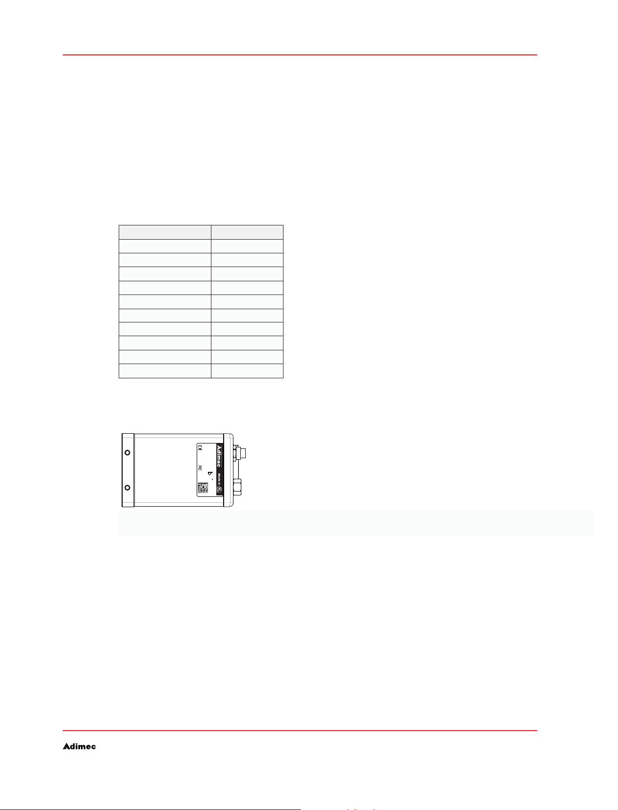
This document applies to the cameras mentioned in Table 1.1. This information can be found on the
camera ID label at the bottom of the camera (see figure 1.1 & 1.2) or via the ID? and BS? command.
Elaborate information about camera identification can be found at chapter 6.
MODEL ISSUE
OPAL-1000m/CL 1.0 - 1.2
OPAL-1000c/CL 1.0 - 1.2
OPAL-1600m/CL 1.1
OPAL-1600c/CL 1.2
OPAL-2000m/CL 1.1
OPAL-2000c/CL 1.0
OPAL-4000m/CL 1.0
OPAL-4000c/CL 1.0
OPAL-8000m/CL 1.0
OPAL-8000c/CL 1.0
OPERATING AND USER MANUAL OPAL FAMILY
Applicable camera modelsTable 1.1:
Type
S/N
: OPAL-XXXXx/x
: XXXXXXXXXXX
RoHS
Issue: X.X
Bottom of the camera with Camera Link interface Figure 1.1:
How this guide is organized1.2
First this guide focuses on the electrical and mechanical installation of the camera. This information
should give enough information to properly design in the camera in the application. Follow up by an
explaining of the different commandos for controlling and configuration the camera. Including the
possibilities to control the camera and the commando structure followed by the explanation of every
commando. At the end of this manual reference information is summarized for easy look up of timing
issues and default camera settings.
7
Page 8

OPERATING AND USER MANUAL OPAL FAMILY
In this manual we use the following standard symbols in the left margin to draw your attention:
ABOUT THIS MANUAL
WARNING
Indicates a hazard that can seriously impair operation.
Do not proceed beyond any of the above notices until you have fully understood
the implications.
Command syntax
Return message
¡
NOTE
(OPTIONAL)
Liability1.3
Every care has been taken in the preparation of this manual. Please inform your Adimec Business
Office of any inaccuracies or omissions. Adimec Advanced Image Systems B.V. cannot be held
responsible for any technical or typographical errors and reserves the right to make changes to the
product and manuals without prior notice. Adimec Advanced Image Systems B.V. makes no warranty
of any kind with regard to the material contained within this document, including, but not limited to,
the implied warranties of merchantability and fitness for a particular purpose. Adimec Advanced Image
Systems B.V. shall not be liable or responsible for incidental or consequential damages in connection
with the furnishing, performance or use of this material.
Layout, composing and editorial staff: Adimec Advanced Image Systems b.v..
Illustrations: Adimec Advanced Image Systems b.v.
Practical tip or note
Function is not standard. For more information obtaining this function please contact your sales representative.
All rights reserved. No part of this document may be reproduced, stored in a database or retrieval
system, or published in any other form or way, electronically, mechanically, by print, photo print,
microfilm or any other means without prior written permission from the publisher.
All correspondence regarding copyrights, translations:
Adimec Advanced Image Systems B.V.
PO Box 7909 Luchthavenweg 91
5605 SH Eindhoven 5657 EA Eindhoven
The Netherlands The Netherlands
Tel: +31 (40) 2353920
Fax: +31 (40) 2353905
URL: www.adimec.com
Publication number: 161585 Manual OPAL FAM rev 1.5
© Copyright 2010 Adimec Advanced Image Systems BV, Eindhoven, The Netherlands.
8
Page 9

OPERATING AND USER MANUAL OPAL FAMILY
9
Page 10

OPERATING AND USER MANUAL OPAL FAMILY
10
Page 11

GENERAL INTRODUCTION
General introduction2.
Congratulations on the purchase of your OPAL camera. Your Adimec camera has been extensively
tested in order to be sure that we delivered a high quality product.
The OPAL camera is designed for Industrial Machine Vision and measurement systems.
The Camera Link digital interface and the size of the camera make electrical and mechanical
interfacing easy. All camera functions are remote controlled. This allows the camera to be optimized
for an integrated application.
Product highlights2.1
The Adimec Machine Vision camera series includes megapixel cameras with the following features:
Platform based product line•
Interline Transfer CCD•
14 bit ADC and channel matching down to sub LSB level•
Extremely low read noise•
Frame buffer for decoupling image acquisition and readout •
Selectable channel remapping in camera•
Horizontal and vertical image flip•
Tight tolerances combined with 100 % factory testing•
Ease of integration through Camera Link standard connection•
OPERATING AND USER MANUAL OPAL FAMILY
Applications2.2
Applications can be found in:
Semiconductor manufacturing•
Electronics manufacturing•
Metrology•
Traffic•
11
Page 12

OPERATING AND USER MANUAL OPAL FAMILY
Camera models2.3
The Adimec Machine Vision camera series are available in several models. Primary differences are the
resolutions and frame speeds.
MODEL RESOLUTION FRAME RATE MONO./COLOR INTERFACE
OPAL-1000m 1024 x 1024 123,1 fps Monochrome Camera Link
OPAL-1000c 1024 x 1024 123,1 fps Color Camera Link
OPAL-1600m 1600 x 1200 69,8 fps Monochrome Camera Link
OPAL-1600c 1600 x 1200 69,8 fps Color Camera Link
OPAL-2000m 1920 x 1080 65,8 fps Monochrome Camera Link
OPAL-2000c 1920 x 1080 65,8 fps Color Camera Link
OPAL-4000m 2336 x 1752 33,5 fps Monochrome Camera Link
OPAL-4000c 2336 x 1752 33,5 fps Color Camera Link
OPAL-8000m 3296 x 2472 17,6 fps Monochrome Camera Link
OPAL-8000c 3296 x 2472 17,6 fps Color Camera Link
Camera models and their main differencesTable 2.1:
RoHS2.4
GENERAL INTRODUCTION
These products comply with the European RoHS directive, 2002/95/EC
Electromagnetic Compatibility (EMC)2.5
This digital equipment fulfills the requirements for radiated emission according to limit B of
EN61000-6-3, and the requirements for immunity according to EN61000-6-2 residential, commercial,
and light industry.
12
Page 13

SAFETY INFORMATION
Safety information3.
General3.1
A CCD camera is a sensitive device. In order to ensure your warranty on this product, please read the
following paragraphs scarefully before you continue to unpack and operate the camera.
Read and follow the instructions – All the safety and operating instructions in this manual should •
be read before and be enforced while the camera is operated.
Retain instructions – The safety and operating instructions should be retained for future reference.•
Perceive the warnings – All actions taken should be executed in compliance with the warnings.•
Do not remove the housing of the camera - There are no user-serviceable parts inside. The •
internal electronics may be damaged by touching the components.
Precautions3.2
It is advised to unpack and handle the camera in a clean, ESD protected work area.•
As long as the lens is not mounted, keep the lens cap in place to prevent dust or contamination •
from entering the CCD sensor or filter area.
Remove the lens cap just before the lens is mounted on the camera. It is advised to perform this •
operation in a clean room or at least a clean bench.
Never touch the CCD sensor surface. The cover glass is easily damaged, and the CCD sensor can •
be damaged by ESD (electrostatic discharge).
OPERATING AND USER MANUAL OPAL FAMILY
Safety symbols3.3
The following safety symbols are applicable to and indicated on the camera.
Symbol for “Conformiteé European”
Handling3.4
In order to prevent damage to the camera and to keep the CCD sensor clean, please pay attention to
the following:
Handle the camera with care. Do not abuse the camera. Avoid striking or shaking it. Improper •
handling or storage could damage the camera.
Do not pull or damage the camera cable.•
During camera use, do not wrap the camera unit in any material. This will cause the internal •
temperature of the unit to increase.
Do not operate camera beyond its maximum operating temperature, humidity and power source •
ratings.
Do not expose the camera to the following environmental conditions:•
Wet, moist and/or high humidity areas. Direct sunlight. High temperature areas. In the vicinity of objects that release strong magnetic or electric fields. In an electrostatic charged environment. Strong vibration. -
Avoid touching the optical surface of the sensor with any object.•
If the optical surface of the sensor needs cleaning, please follow the directions •
in chapter 9.4; ‘Cleaning‘.
The housing is susceptible for scratches. When cleaning the camera, use a soft cloth.•
13
Page 14

OPERATING AND USER MANUAL OPAL FAMILY
SAFETY INFORMATION
14
Page 15
INSTALLATION
Installation4.
Camera Link at Base configuration is a universal way of connecting the CL series camera to a
framegrabber and suitable for high speed applications.
The OPAL camera is also available with Coaxpress or GigE Vision interface. It goes beyond the
scope of this manual to elaborate on this. Please contact your local sales representative for further
information.
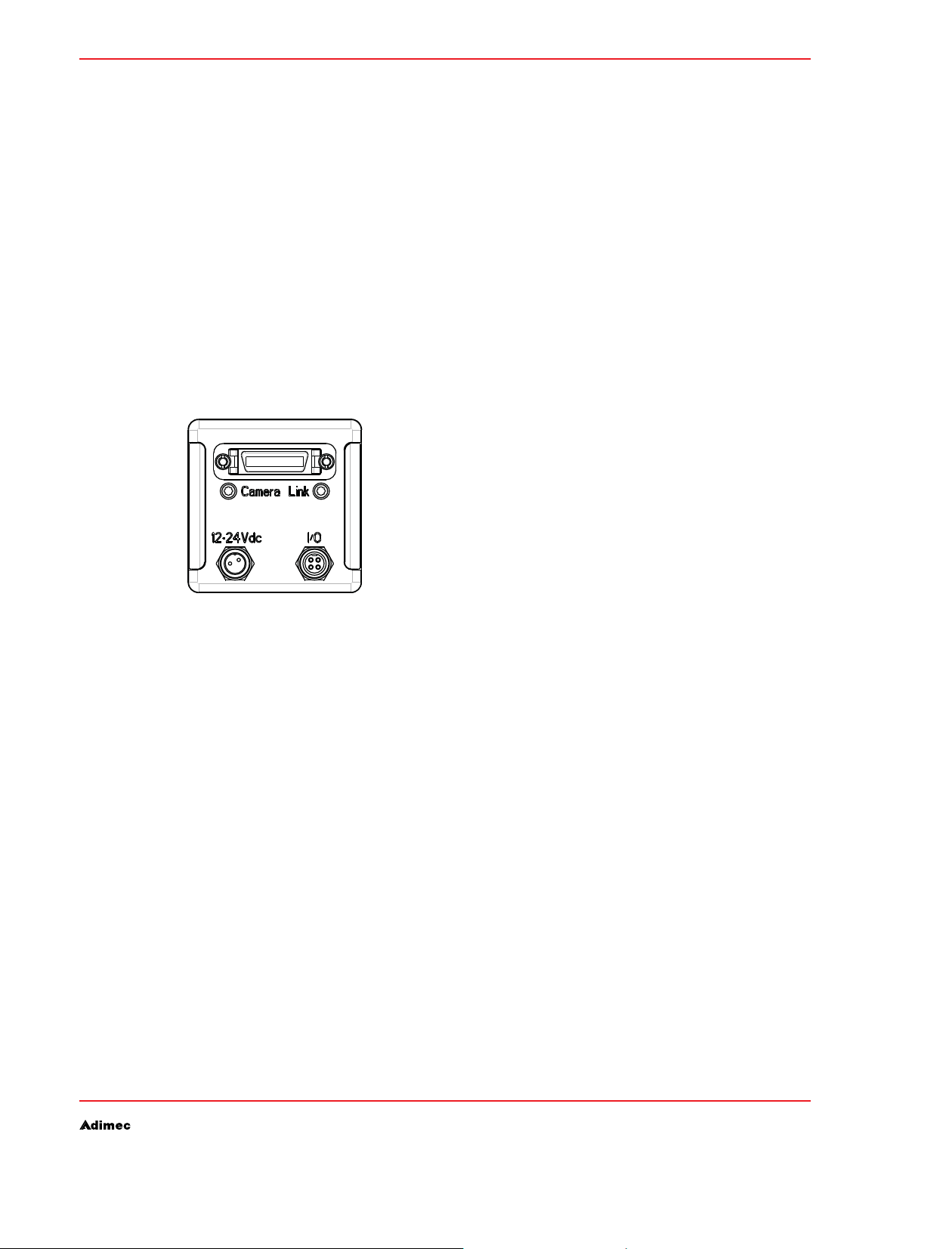
OPAL interface connections4.1
The camera is equipped with several connectors for the following functions:
OPERATING AND USER MANUAL OPAL FAMILY
Power•
I/O•
Video and Data•
Backside of the cameraFigure 4.1:
Power supply4.1.1.
The camera must be powered by a DC power supply.
All cameras adapt automatically to a wide range of input voltage. There is no galvanic isolation
between input power lines and internal power lines.
For safety, peripheral equipment must be either double isolated or SELF qualified.
15
Page 16

OPERATING AND USER MANUAL OPAL FAMILY
Power connector OPAL camera
Chassis part
Binder series 712 type 09-0403-00-02 -
1
2
Camera male power connectorFigure 4.2:
PIN FUNCTION
1 10.2 to 27.6 Vdc
2 GND
Power pin configuration for OPAL-1000.Table 4.1:
CAMERA CL MODEL POWER REQUIREMENT
OPAL-1000 < 5 Watt @12 Volt
OPAL-1600 < 6 Watt @12 Volt
OPAL-2000 < 6 Watt @12 Volt
OPAL-4000 < 6 Watt @12 Volt
OPAL-8000 < 6 Watt @12 Volt
Power requirement Camera Link series cameras.Table 4.2:
INSTALLATION
NOTE: The supply is reverse voltage protected. When applying power to the camera with the wrong
polarity it will not operate, but will not be damaged also.
Mating cable connector:
Binder series 711 type 99-0072-100-02 (straight) Binder series 712 type 99-0402-00-02 (straight) Binder series 712 type 99-0402-70-02 (90 degrees angle) -
Power cable
All OPAL cameras can be delivered with a power cable (2 meter) as accessory. It is available as
Adimec part no. 102830
WIRE FUNCTION
White Positive (12 - 24 Vdc)
Brown Negative (return)
Shield Mechanical ground
Power pin configurationTable 4.3:
All other wires are not used and should not be connected.
16
Page 17
INSTALLATION
I/O Interface4.1.2.
I/O connection
An input for external triggering of the camera is available at the I/O connector.
Also a trigger output signal from the camera to control an external flash light is available at this
connector. The input and output are fully programmable. For reference see par 7.8.
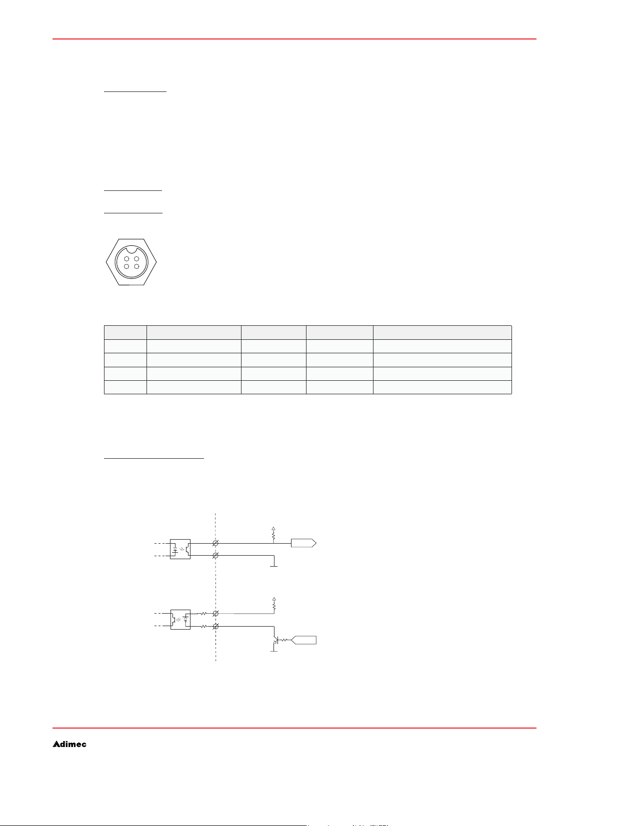
The input and output are galvanic isolated from the internal camera electronics by means of an
optocoupler.
I/O connector
Chassis part:
OPERATING AND USER MANUAL OPAL FAMILY
Binder series 711 type 09-0082-20-04 -
1
4
3
2
Camera female I/O connectorFigure 4.3:
PIN NO. SIGNAL NAME DIRECTION LEVEL AT THE PIN
1 Flash strobe out Output Open collector of optocoupler
2 Trigger in Input 10..20 mA Anode of optocoupler(*
)
3 Trigger return Input Isolated gnd Cathode of optocoupler
4 Flash strobe return Output Isolated gnd Emitter of optocoupler
I/O pin configuration.Table 4.4:
(*)
serial resistors 2x 220 Ω inside Installationcamera.
Mating cable connector
Binder series 711 type 99-0079-100-04 (straight) Binder series 712 type 99-0409-00-04 (straight) Binder series 712 type 99-0409-70-04 (90 degrees angle) -
Flash strobe out
Trigger in
Camera Application
1
4
2
220 Ω
220 Ω
3
I/O Connector
Vext
R1 EXT
Flash
BGND
Vext
R2 EXT
Trigger
BGND
Circuit concept of I/O.Figure 4.4:
17
Page 18
OPERATING AND USER MANUAL OPAL FAMILY
NOTE: The delay from non-conductive to conductive state of the phototransistor is less than 1.5 μs.
The delay from conductive to non-conductive state of the phototransistor is less than 10 μs.
The recommended termination circuitry is drawn in Figure 4.4.
A current of 2.5 mA is recommended for the Flash output. For the trigger input a current of 10 mA is
recommended. These current recommendations translate to the recommended resistor values in table
4.5.
VEXT [V] R1 EXT [Ω] R2 EXT [Ω ]
3.3
5.0 2000 0
12 4700 470
1000
Recommended series resistor for trigger inputTable 4.5:
Do not apply
Video and Data interface4.1.3.
Camera Link
The Camera Link output is designed to connect the camera to a Frame Grabber, in order to transmit
the video and to control the camera settings. It is implemented according to the international Camera
Link specification, described in the Camera Link Interface Standard for Digital Cameras and Frame
Grabbers – Version 1.1 of January 2004.
The maximum theoretical cable length is 7 meter at the rated pixelclock frequency. However, the
maximum attainable Camera Link data transmission distance is subject to cable performance, physical
connection setup, balance, skew, and clock speed, therefore application dependent.
INSTALLATION
Camera Link Connector
Camera Link connector type: 3M MDR 26-pins.
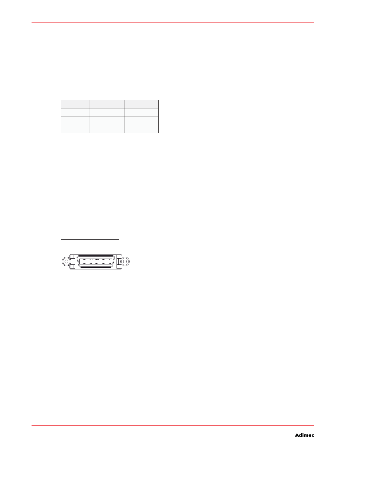
Female Camera Link connector at the camera.Figure 4.5:
Standard Camera Link cables can be ordered at Adimec.
WARNING: Avoid damage by preventing the entry of foreign objects or dirt to the connectors. The
tightening torque for the retention screws may not exceed 0.29 Nm.
Camera Link ports
The two video outputs TAP-A and TAP-B of the camera are mapped to the Camera Link ports A, B and
C as defined in the Camera Link specification. It is set up as a Camera Link Base configuration and
therefore uses one Camera Link connector.
More information about Camera Link configuration can be found in par 10.1.
18
Page 19
INSTALLATION
Mechanical4.2
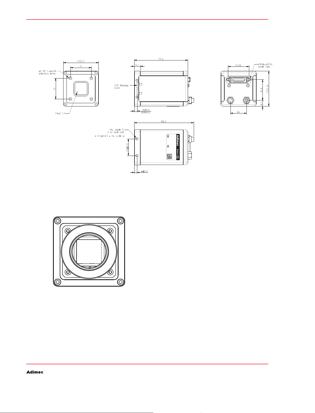
Outline dimensions Camera Link series camera4.2.1.
OPERATING AND USER MANUAL OPAL FAMILY
Camera Link
12 - 24 Vdc
Type
S/N
: OPAL-XXXXx/x
: XXXXXXXXXXX
RoHS
Issue: X.X
Camera outline drawing Camera Link camera.Figure 4.6:
I/O
Lensmount4.2.2.
4 Torx screws that hold the C-format lensmount (front view of the camera)Figure 4.7:
Upon delivery, the OPAL1000, 1600, 2000 and 4000 cameras are fitted with a C-format lensmount by
means of four screws as indicated in figure 4.7. To prevent damage and contamination of the CCD a
protective plastic cap is placed on the lensmount.
The OPAL8000 camera will be delivered without lensmount.
The OPAL-8000 camera has an 18.13mm (H) x 13.60mm (V) 22.66mm (diag) sized, 4/3” format CCD.
Some applications may requires a lensmount and lens in accordance to the optical format listed.
19
Page 20
OPERATING AND USER MANUAL OPAL FAMILY
Vignetting can be expected with F# values smaller than F4 when using a C-format lensmount.
NOTE: The protective cap may only be removed by pulling it off. Never try to unscrew the protective
cap as this will dissasemble the C-format lensmount.
IN ORDER TO PREVENT DAMAGE TO THE CAMERA AND TO KEEP THE CCD CLEAN, PLEASE
TAKE THE FOLLOWING PRECAUTIONS.
• Always keep the lens cap in place, as long as no lens is attached.
• Pull off the lens cap by just before the lens is screwed on the camera. It is advised to perform this
operation in a clean room or clean bench.
• Never touch the CCD surface. The cover glass is easily damaged, and the CCD can be damaged by
electrostatic discharge (ESD).
Mounting facilities for system integration4.2.3.
In order to provide the facility to integrate the camera into a system, the camera is provided with
mounting holes in the top, bottom and left and right sides of the front. See figure 4.6 & 4.8 for more
details.
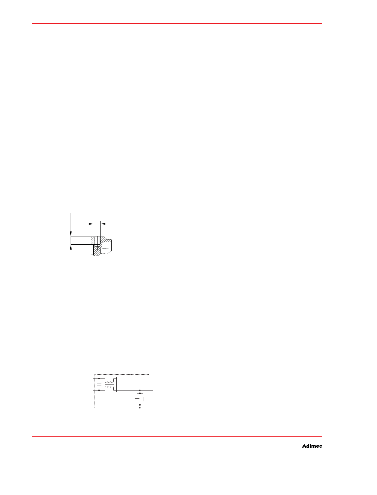
WARNING: The length of the thread is 5 mm. The tightening torque for the retention screws may not exceed
1.9 Nm. To prevent damage, do not use bolts which will exceed the length of the tread. See fi gure 4.8 for
more details
INSTALLATION
5 mm
Maximum length of tread.Figure 4.8:
M4
Environmental4.3
EMC/EMI – ESD4.3.1.
The camera complies to the requirements of EN61000-6-2 and EN61000-6-3.
In order to obtain the best performance, the camera and the connected cables should be shielded
from environmental noise sources.
Avoid possible ground loops when integrating in a system. Notice the following circuit diagram.
power in
power return
smps
c = < 220 uF
I/O reference
R = > 82kΩ
20
Simplified diagram of connections in the cameraFigure 4.9:
Page 21

INSTALLATION
Take appropriate precautions to prevent ESD:
The camera is shipped in a special bag designed to prevent ESD. For storage, keep the device in the
bag.
Thermal management4.4
Like any CCD sensor based camera, optimal performance is achieved by leading the heat away from
the sensor. Keeping the sensor circuit relatively cool reduces the amount of dark current generated
within the CCD sensor. Dark current is the major contributor to Fixed Pattern Noise, Dark Signal NonUniformity and other read noise effects. This harms the performance, especially when video is gained
to a large extension. In general, the dark current is doubled with every 7ºC increase in temperature of
the sensor. Also the dark current increases linearly with the integration time. The camera is designed
to operate at an ambient temperature between -10 ºC and +50ºC.
OPERATING AND USER MANUAL OPAL FAMILY
Never insert a metal tool or knife into the bag and rip it open, but open it by hand. It is advised •
to keep this bag; If it is ever needed to transport the device, the bag is the first line of protection
from ESD.
It is advised to wear an ESD wrist strap connected to the ground of the electrical system.•
If a wrist strap is unavailable, touch a grounded part of the system before handling the camera.•
Avoid touching the connector pins on the camera with bare fingers or tools.•
Protect the camera from high power electrical fields as generated in fans or high voltage power •
supplies.
This camera is mechanically designed for optimal thermal conductance from the sensor to the solid
front of the camera, in order to keep the sensor at the lowest temperature possible.
When integrating into a system and running at an ambient temperature up to 50ºC, it is advised to take
proper measures to dispose of the heat in order to gain optimal performance. Heat disposal from the
front assembly can be improved by mounting the camera to a solid metal base. Also mounting heat
sinks to the remaining sides of the front may contribute to the disposal of heat. Another method to
carry away the heat is natural or forced convection.
21
Page 22

OPERATING AND USER MANUAL OPAL FAMILY
22
Page 23
CONTROL OF THE CAMERA
Control of the camera5.
Introduction5.1
The camera is fully software controlled via the Camera Link serial channel using a simple ASCII based
protocol. It is possible to save settings as ‘power-up default settings’ in the camera.
Basically there are three ways to control the camera:
By means of the Adimec easy-to-use Windows Control application•
By means of the Adimec Command Console application•
By means of your own dedicated software•
In addition to an explanation on how to use the Adimec communication applications, you will also
find a description of the command structure. This description should be read and understood when
controlling the camera either with the Adimec Command Console application or with your own
dedicated software.
Par 10.4 gives an overview of the camera commands and the possible ranges.
Controlling with the Windows Control application5.2
The Windows Control application will run on W9x, NT, 2000 and XP (32 bit) operating systems and in
32 bit mode on Vista (64bit) systems.
It does not need installing, simply copy the files to a dedicated directory on the hard disk drive.
OPERATING AND USER MANUAL OPAL FAMILY
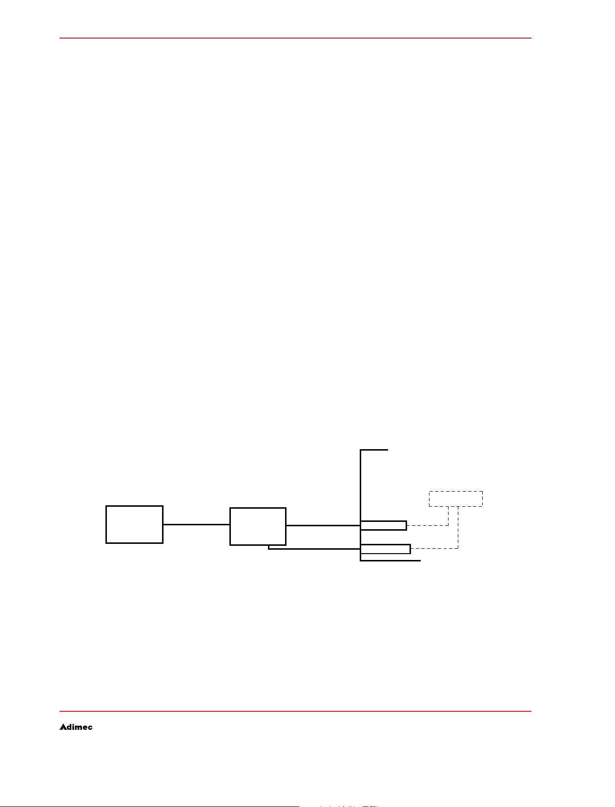
NOTE: The serial control signals of the camera needs to be mapped onto a communication channel,
either by means of a hardware breakout circuit (to a hardware COM-port) or by mapping the control
signals onto a serial communication channel supported by the Frame Grabber. In Figures 5.1 and
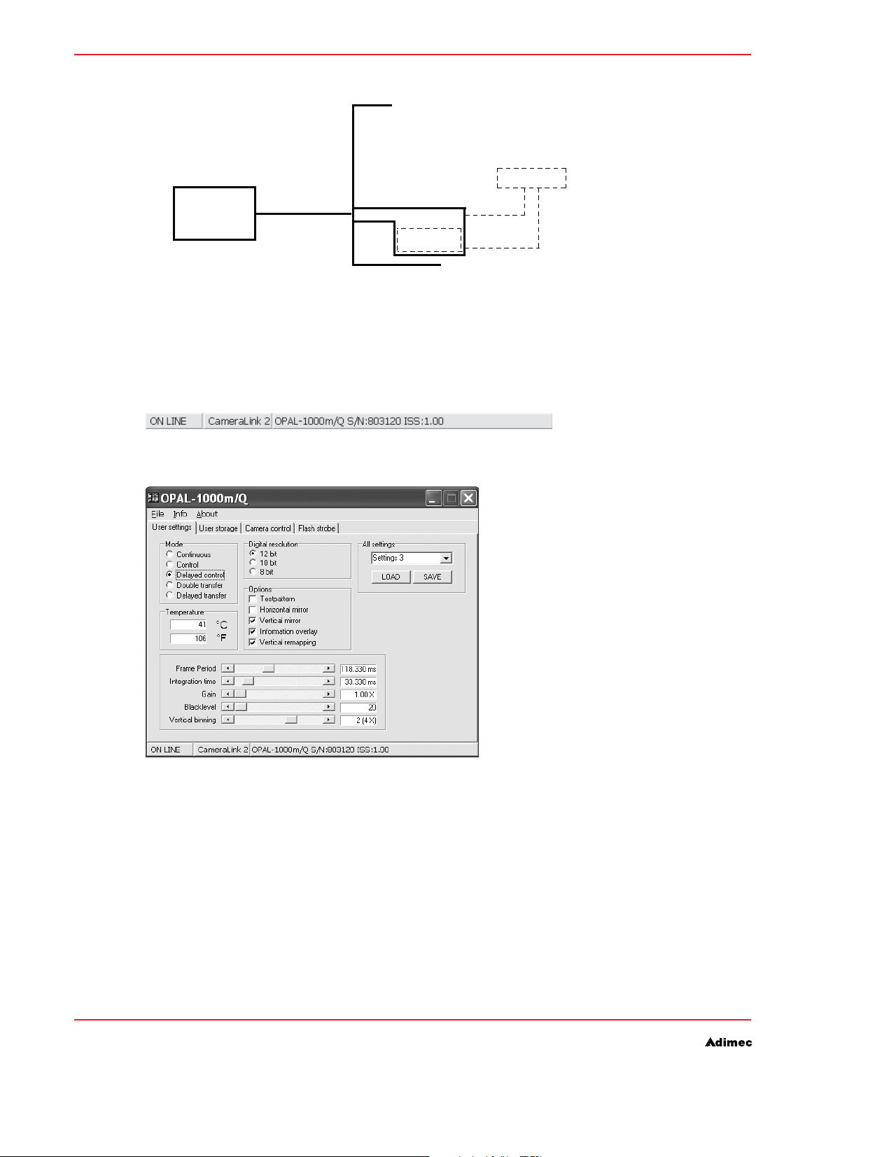
5.2 both possibilities are depicted in a simplified diagram. The camera in these pictures can either
be a Camera Link version or a CoaXPress version (CL with additional CXP interfacebox or CXP Frame
Grabber).
Camera
Camera Link mapped by means of a hardware breakout boxFigure 5.1:
- Video
- Ext. control
- Serial com
Breakout
box
- Video
- Ext. control
- Serial com
Computer
framegrabber
serial COM port
application
image data
camera control
23
Page 24
OPERATING AND USER MANUAL OPAL FAMILY
CONTROL OF THE CAMERA
- Video
Computer
application
- Ext. control
Camera
Camera Link mapped by means a virtual COM-port supported by the Frame Grabber Figure 5.2:
- Serial com
framegrabber
Comm. channel
image data
camera control
Dashed = software
Solid = hardware
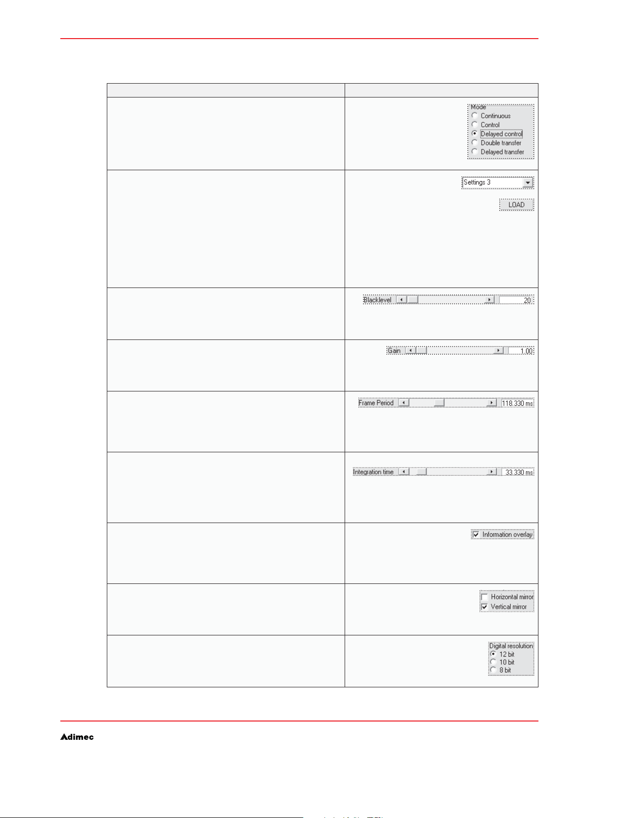
After launching the application it will autodetect the COM-port number or other communication
channel. Make sure to select the correct COM-port.The application will then check communication and
if OK, it will read the camera type and serial number from the camera and display the information in
the status bar.
Example status barFigure 5.3:
24
User interface example of windows control applicationFigure 5.4:
All basic functions of the camera can be controlled by an intuitive user interface. These functions are
accessable via different tabs at the top of the application. The following tabs are available
User settings tab•
User storage tab•
Additional settings tab (only available for color)•
Camera control tab•
Flash strobe tab•
NOTE: Depending on camera model, available settings and options are shown.
Page 25
CONTROL OF THE CAMERA
User settings tab5.2.1.
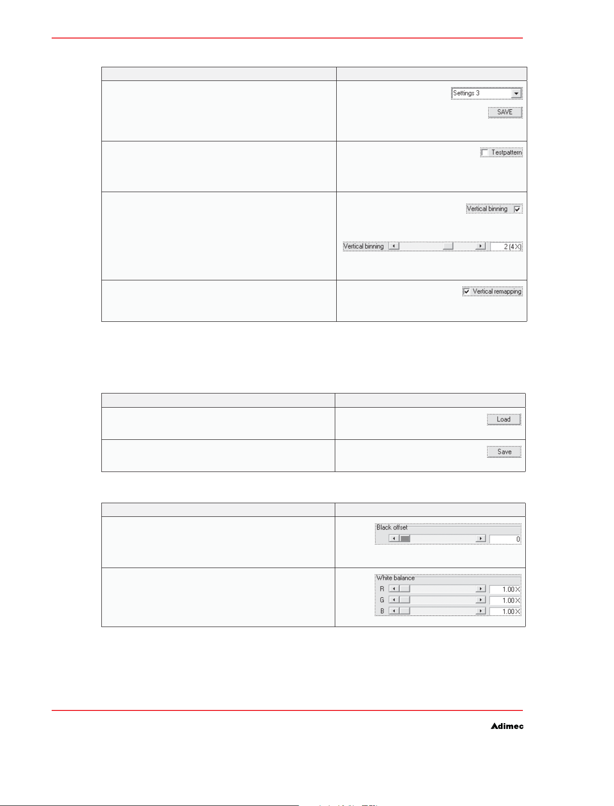
FUNCTION CONTROL
Acquisition mode
In the frame Mode, one of the different Image acquisition
modes can be set. The Continuous and Control modes are
standard. Delayed control, Double transfer, Delayed transfer
are optional. More information regarding image acquisition
can be found in chapter 7.
Activate stored camera settings
Up to nine user defined sets of power-up settings can be
stored in the camera. These are power-up sets 1-9. Power-up
set 0 is the factory default setting. Every power up set contains the values of every tab, except the values of the User
storage. The user can choose from which power-up set the
camera will power-up.
Choose in the drop down box the desired power-up setting and press LOAD. The values of the desired settings are
shown in the application and the camera is working according to the loaded settings
Blacklevel, only for monochrome
With slider Blacklevel, the offset can be set in order to enable
all captured information to be displayed within the digital
domain. More information can be found in chapter 8.
OPERATING AND USER MANUAL OPAL FAMILY
Digital gain
With slider Gain, the programmable amplifier can be set to
apply gain in the signal path. More information can be found
in chapter 8.
Frame period
With slider Frame Period, the frame period in units of 10 us
can be set. More information about frame periods in the different image acquisition modes can be found in chapter 7.
The setting is only valid when in continuous mode.
Integration time
With slider Integration time, the frame period in units of 10 us
can be set. More information about integration times in the
different image acquisition modes can be found in chapter 7
The setting is only valid when in continuous mode.
Information overlay
When enabled, the top left most active video pixels in the
output image are replaced by 8 data pixels. The upper 8 bits
of the data pixels carry information, lower bits (when applicable) are set 0.
Mirroring
With the checkboxes Vertical mirror and Horizontal mirror
the output image can be vertical and/ or horizontal mirrored.
More information can be found in chapter 8
Output resolution
In the frame Digital resolution, the bit depth of the camera
output can be set by this parameter, Resolutions of 8, 10 and
12 bit are standard.
25
Page 26
OPERATING AND USER MANUAL OPAL FAMILY
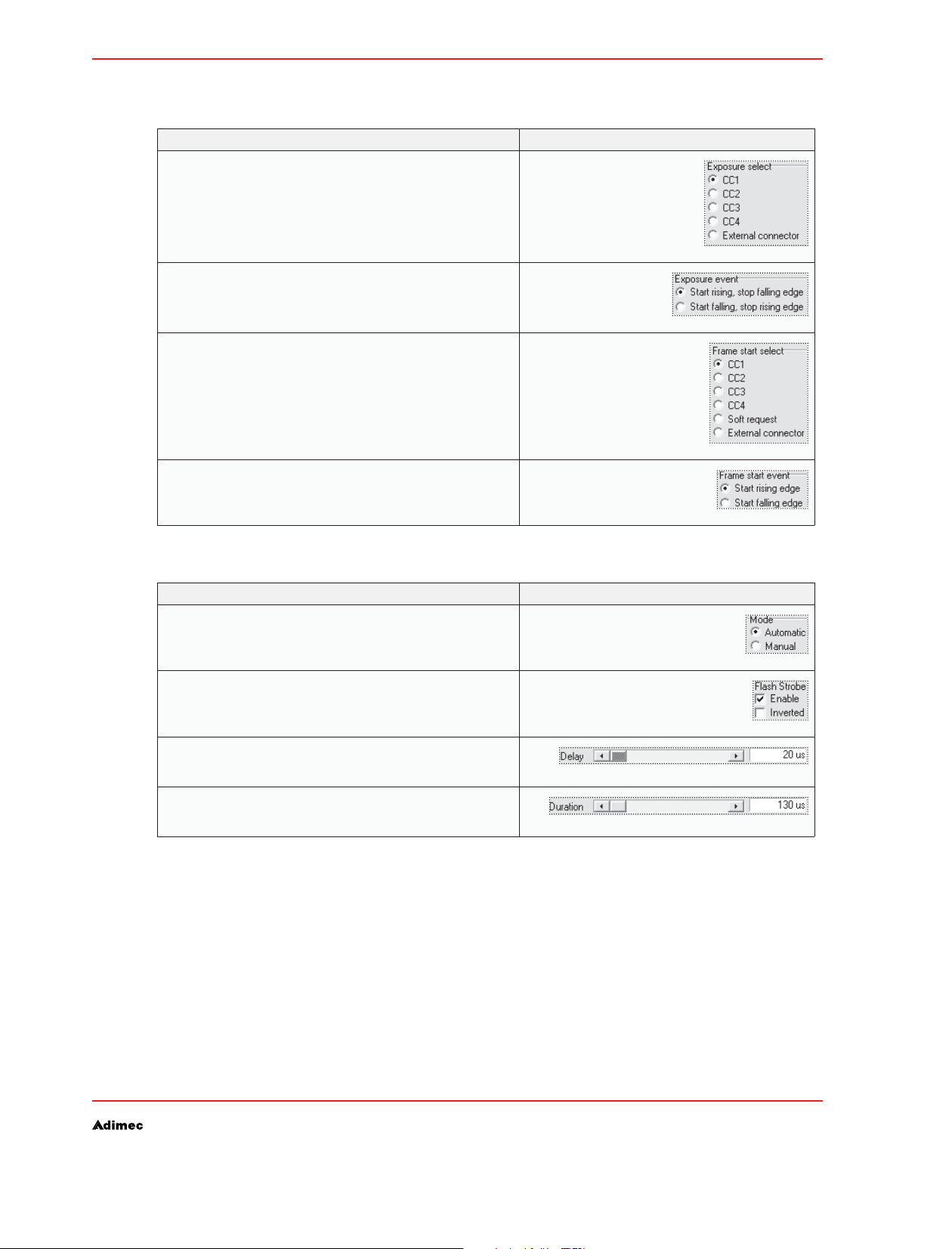
FUNCTION CONTROL
Store camera settings
The actual settings of every tab, except the settings of tab
User storage, will be stored simultaneously. To store the
current settings select the desired settings from 1 to 9 in the
drop down box and press SAVE.
Testpattern
With checkbox Testpattern the testpattern on the output
image can be set. More information about interpreting the
testpattern can be foud in chapter 9
CONTROL OF THE CAMERA
Vertical binning
With checkbox/ slider Vertical Binning, it is possible to
combine two, four or eight lines of video on the CCD before
reading out. When applying binning it is possible to achieve
higher frame rates. The standard option can be selected by
means of a checkbox. If the option extra binning is enabled
the binning is set by means of a slider. More information can
be found in chapter 8.
Vertical remapping
When enabled the data from the CCD will be re-arranged in
order to provide normal left-to-right, top-to-bottom scanning.
More information can be found in chapter 8.
Standard
Optional
User storage tab5.2.2.
This tab can be used for storage of camera related values / labels, such as calibration data, specific
settings, position in the application, etc. Data can be saved as a maximum of 15 integers and a
maximum of 15 strings.
Function
Load camera related values
To load every camera related value press Load
Store camera related values
Values are not automatically stored into the camera memory.
To store the current values press Save.
CONTROL
26
Additional settings tab (only available for color)5.2.3.
FUNCTION CONTROL
Black offset
With slider Black offset, the offset can be set in order to
enable all captured information to be displayed within the
digital domain. More information can be found in chapter 8
White balance
With the slides R(ed), G(reen) and B(lue) the additional gain
per color channel can be programmed in order to correct for
different illumination colors. More information can be found
in chapter 8.
Page 27
CONTROL OF THE CAMERA
Camera control tab5.2.4.
OPERATING AND USER MANUAL OPAL FAMILY
Function
Exposure select
In the frame Exposure select, the method of controlling the
exposure start trigger can be selected. This can be done
by each and every one of the CC1..CC4 of the Camera Link
connector or the external trigger input on the I/O-connector.
More information can be found in chapter 7
Exposure event
Determines the activation of exposure on rising or falling
edge.
Frame start select
In the frame Frame start select, the method of controlling
the frame start trigger can be selected. This can be done
by each and every one of the CC1..CC4 of the Camera Link
connector, a soft request or the external trigger input on the
I/O-connector. More information can be found in chapter 7.
Frame start event
Determines the start of read out on rising or falling edge.
Flash strobe tab5.2.5.
CONTROL
Function
Mode of flash strobe operation
In automatic mode the flash strobe output will be active
during the integration of the image. When set to manual, the
behaviour of the flash during exposure can be programmed.
Flash strobe output
The flash strobe output can be enabled if the option is selected. The output can reverse polarity when selected.
Flash strobe delay
If manual mode is selected, the start delay of the strobe
output can be set by the slider.
Flash strobe duration
If manual mode is selected, the active duration of the strobe
output can be set by the slider.
CONTROL
27
Page 28

OPERATING AND USER MANUAL OPAL FAMILY
Controlling the camera with the Command Console application5.3
The Command Console application is a basic communication console. Commands entered at the
prompt line are directly sent to the camera. The program will run on W9x, NT, 2000 and XP (32 bit)
operating systems and in 32 bit mode on Vista (64 bit) systems.. It does not need installing, simply
copy the files to your hard disk drive.
NOTE: The serial control signals of the camera needs to be mapped onto a communication channel,
either by means of a hardware breakout circuit (to a hardware COM-port) or by mapping the control
signals onto a serial communication channel supported by the Frame Grabber. In Figures 5.1 and 5.2
both possibilities are depicted in a simplified diagram. The camera in these pictures can either be a
Camera Link version or a CoaXPress version (CL with additional CXP interfacebox).
Before launching the program the correct COM-port number must be entered by editing the console.ini
file. Replace the line PORT=0 by PORT=x, where x = your COM-port number minus 1. In case of serial
communication per Camera Link interface, set CLSELECT to 1.
Controlling the camera with your own dedicated software5.4
The camera can also be controlled by a host system connected to the Camera Link interface using the
serial communication link of the Camera Link. Commands and resulting data are transferred between
the host system and the camera according to the communication protocol as defined in par 10.3. The
camera will always act as slave in the communication link, the host system must be master. All actions
are initiated by the host system, the camera only replies on messages received from the host system.
CONTROL OF THE CAMERA
Command structure5.5
Introduction5.5.1.
When the camera is controlled by means of the Console Application or with your own dedicated
software, the following command structure is used.
Parameters5.5.2.
Most camera o peration commands need one or more parameters. In general the command therefore
consists of a command keyword and the required parameters for that specific command. If more
parameters are required they should be separated by a semicolon (;).
Almost all parameters are signed integer values. Negative values must start with a minus sign
character (-). A plus sign character (+) for positive values is allowed, but not required.
For some commands a parameter may consist of a string of characters rather than a number. In that
case this string must be preceded by the double-quote sign character (“).
Commands accompanied by the wrong number of parameters are ignored.
Command example:
Command syntax: WB100;150;235
28
Page 29

CONTROL OF THE CAMERA
Request commands5.5.3.
Actual camera settings can be obtained via a request command. Commands with a question mark
after the keyword are recognized as request commands.
Request command example:
Command syntax: BS?
The camera will reply with one or more parameters, separated by a semicolon (;) if necessary. Reply
values are always preceded with minus sign character (-) when negative and a plus sign character (+)
when positive.
If a reply is a string of characters rather than a number then this string is preceded by the
double-quote sign character(“).
Reply message example:
Reply message: “1.0A;1.21;1.00
Where 1.0A;1.21;1.00 represents the camera information.
OPERATING AND USER MANUAL OPAL FAMILY
29
Page 30

OPERATING AND USER MANUAL OPAL FAMILY
30
Page 31

MANAGING CAMERA SETTINGS
Managing Camera Settings6.
Introduction6.1
Operation of the camera is defined by a number of settings, controlled by various commands. When
the camera is powered initially, the camera will power-up in a defined mode, with all parameters in
‘power-up default’ setting. This is called power-up set 0. This default power-up set 0 is determined by
Adimec can not be altered.
Instead, up to nine additional user defined sets of power-up settings can be stored. This way, user
defined settings can be applied at powering up.
Load Power-up defaults and choose power-up set6.2
At any moment all camera settings and parameters can be reverted back to one of the standard
power-up settings by means of the load configuration command.
Command syntax: LCx
where x = power-up settings set number (see table 6.1).
SETTING (X) FUNCTION
0 Factory default
1..9 User defined
OPERATING AND USER MANUAL OPAL FAMILY
Possible power-up defaultsTable 6.1:
NOTE: The next time the camera is powered, it will start with the power-up settings set number x.
The number of the last selected power-up default can be read back from the camera:
Command syntax: LC?
Reply message: x
Where x = as in table 6.1
Change power-up defaults6.3
To save the current camera configuration as a power -up settings set, the save configuration command
must be used.
Command syntax: SCx
Where x = power-up settings set number
NOTE: x=0 is not allowed, because the factory default set cannot be altered
NOTE: An additional LCx command is needed to make the camera power-up in these settings.
31
Page 32

OPERATING AND USER MANUAL OPAL FAMILY
Obtaining the camera identification string6.4
For identification purposes the camera model and serial number can be requested by the identification
command.
Command syntax: ID?
Reply message: a -bc/x[f] S/N:e
Where a is the family name OPAL
b is the detector type e.g. 1000, 2000, etc
c is c for color and m for monochrome
x is D or Q for Dual or Quad sensor output
[f] [optional] the customer special string
e is the camera serial number string
Example:
CAMERA MODEL REPLY MESSAGE
OPAL-1000m/CL OPAL-1000m/CL S/N:xxxxxxxxxxx
OPAL-1000c/CL OPAL-1000c/CL S/N:xxxxxxxxxxx
MANAGING CAMERA SETTINGS
Where xxxxxxxxxxx = serial number
Example of the replied ID messages for monochrome and color camerasTable 6.2:
Obtaining the camera model identification6.5
The model identification (Adimec Part ID) can be obtained from the camera by means of the Model
Identification command.
Command syntax: MID?
Reply message: “xxxxxx
Where xxxxxx = Adimec Part ID.
Obtaining the camera Serial Number6.6
The serial number can be obtained from the camera by means of the Serial Number command.
Command syntax: SN?
Reply message: “xxxxxxxxxxx
Where xxxxxxxxxxx = serial number.
NOTE: When requesting support on some features of the camera, Adimec may request the serial
number of the camera, in order to optimize support.
32
Page 33

MANAGING CAMERA SETTINGS
Obtaining the camera build state6.7
The camera issue and firmware revisions can be obtained from the camera by means of the Build
State command..
Command syntax: BS?
Reply message: “x.xx;y.yy;z.zz
Where x.xx stands for camera issue, y.yy indicates the microcontroller fimware version and z.zz
indicates the FPGA firmware version.
NOTE: When requesting support on some features of the camera, Adimec may request the build state
information, including firmware versions, in order to optimize support.
User storage6.8
Up to 16 user-defined strings and 16 user-defined signed integers can be stored in the camera for user
reference. These parameters do not have any effect on camera performance.
Setting one of the 16 user integers is done by means of the USI command
Command syntax: USIx;y
OPERATING AND USER MANUAL OPAL FAMILY
Where x = user integer index [0…15]
y = user integer value.
Reading back one of the 16 user integers is done by means of the USI? command
Command syntax:USI?x
Reply message: y
Where x = user integer index [0…15]
y = user integer value.
Setting one of the 16 user strings is done by means of the USS command
Command syntax: USSx;”y
Where x = user string index [0…15]
y = user string value (maximum length is 32 characters).
Reading back one of the 16 user strings is done by means of the USS? command
Command syntax for readback:USS?x
Reply message: y
Where x = user string index [0…15]
y = user string value.
33
Page 34

OPERATING AND USER MANUAL OPAL FAMILY
34
Page 35

IMAGE CAPTURING AND VIDEO OUTPUT
Image capturing and video output7.
Introduction7.1
Image acquisition is possible in several modes. In this chapter each mode is described in a separate
paragraph.
Some general remarks:
Image Acquisition takes some time, depending on camera settings. In either mode, if the user •
tries to capture frames at a higher frame rate than the acquisition time allows, the camera will not
behave as expected.
If images are captured continuously, an integration time larger than the frame period is not •
possible.
To make use of the camera’s maximum speed, it is in general necessary to start acquiring frame •
number n, while frame number (n-1) is still being read out through the Camera Link interface.
In general, as with all CCD cameras, sensor exposure time is controlled by performing an electronic
shutter action. This action (in timing diagrams referred to as exposure) represents exposure duration or
integration time.
NOTE: In the paragraphs describing the control modes, it is assumed that the trigger polarity is normal
and that the trigger signals exposure and read-out are controlled by the CC1 input.
OPERATING AND USER MANUAL OPAL-FAMILY
It is however also possible to choose one of the other camera control signals (CC2 - CC4) or the
external trigger input on the I/O-connector for trigger input. It is even possible to use two different
control signals; one for exposure control and another one to control the read-out timing.
The selection and behavior of the control signals are explained in detail in par. 7.10 and 7.11.
Selecting Image Acquisition Mode7.2
Image acquisition mode is selected by the mode command
Command syntax: MOx
where x indicates acquisition mode, depending on camera model, according to table 7.1.
The actual mode can be read back from the camera:
Command syntax: MO?
Reply message: x
where x indicates acquisition mode, depending on camera model, according to table 7.1.
CAMERA MODEL MO0 MO1 MO2* MO3* MO4* MO5*
OPAL-1000
OPAL-1600
OPAL-2000
OPAL-4000
OPAL-8000
* optional
Continuous Normal
control
Delayed
transfer
Double
Transfer
Double
Delayed
Transfer
IT defined
integration
control
Camera acquisition modesTable 7.1:
35
Page 36
OPERATING AND USER MANUAL OPAL-FAMILY36IMAGE CAPTURING AND VIDEO OUTPUT
Used parameters and timing table7.3
The next paragraphs about the acquisition modes make use of timing diagrams. These diagrams list
parameters that are gathered in table 7.2 below.
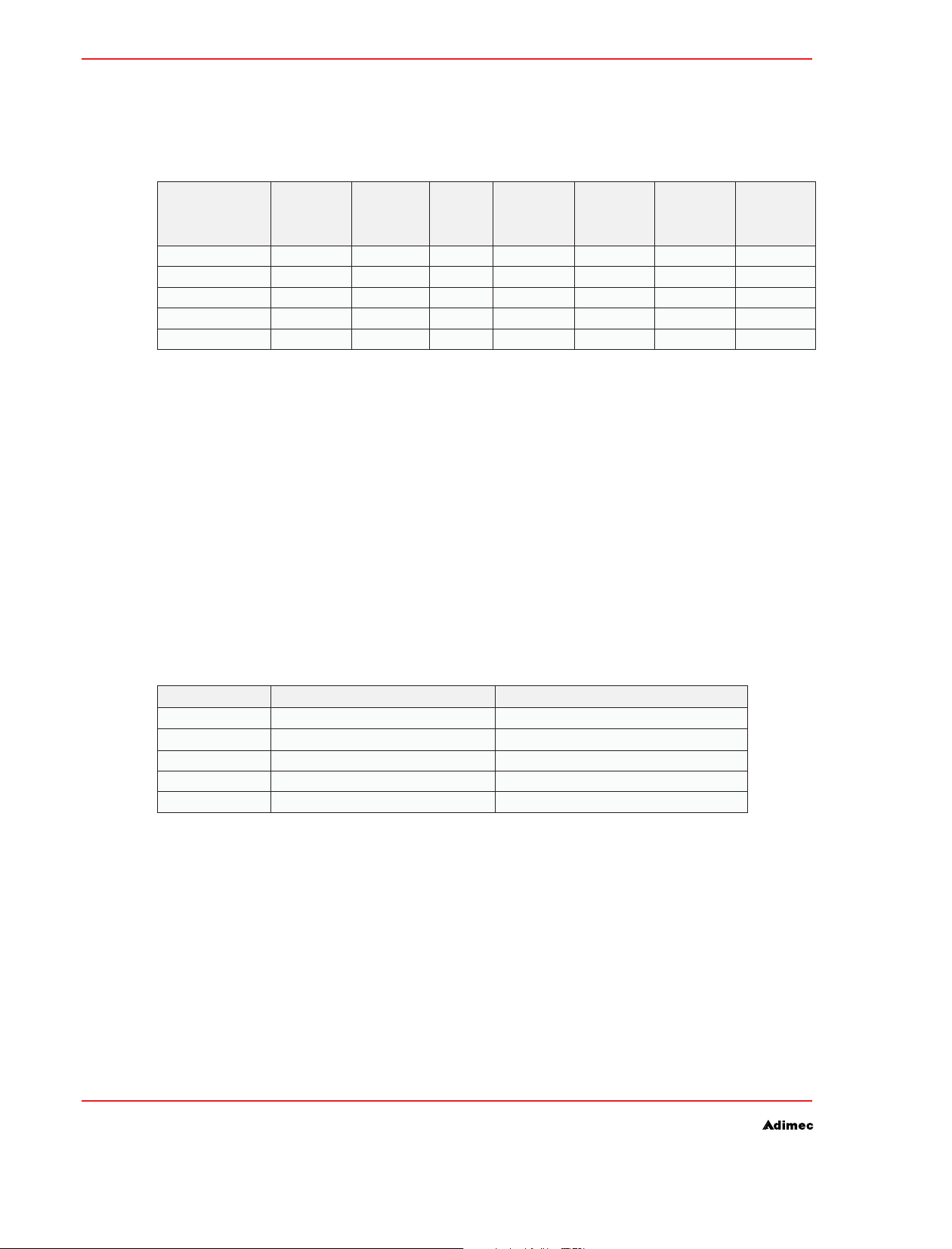
CAMERA MODEL TD_IT_BGN TD_IT_END T_DTM_
GAPMIN
OPAL-1000 2 μs 7.5 μs 26 μs 8,127 ms 4,637 ms 2,889 ms 2,029 ms
OPAL-1600 2 μs 7.5 μs 26 μs 14,332 ms 7,850 ms 4,612 ms 3,000 ms
OPAL-2000 2 μs 7.5 us 26 μs 15,189 ms 8,227 ms 4,749 ms 3,028 ms
OPAL-4000 2 μs9 μs 26 μs 29,833 ms 16,791 ms 10,275 ms 7,045 ms
OPAL-8000 2 μs 10 μs 26 μs 56,917 ms 31,077 ms 18,163 ms 11,739 ms
* optional
Timing detailsTable 7.2:
T FRAMEMIN
@ NO BINNING
T FRAME
MIN
@ 2 LINES
BINNING
T FRAME
MIN
@ 4 LINES
BINNING*
T FRAME
MIN
@ 8 LINES
BINNING*
A short explanation of the timing parameters in this table: There is some time needed to apply a
shutter pulse to the CCD. The CCD will start integrating light (start of exposure) at a shutter action.
Integration will start td_it_bgn after the rising edge of the shutter pulse.
During the time needed to transfer the image from the photo-sensitive area to the storage area, the
CCD will continue to integrate during a short period of time being td_it_end. In other modes than
continuous mode there is an additional demand in timing.
T_dtm_gapmin is only applicable in double transfer mode and double delayed transfer mode.
T_dtm_gapmin lists the minimal time between 2 exposures.
Td_output is the figure for the delay between end of acquisition and start of output. The Vertical
Remap function determines the method of transmitting the pixels at the output. For an extensive
explanation of Vertical Remap refer to par 8.5. Enabling Vertical Remap influences the delay time to
the output. The delay is listed in table 7.3 for the various models.
CAMERA MODEL
OPAL-1000 ≤ 410 μs ≤ 4700 μs
OPAL-1600 ≤ 720 μs ≤ 7900 μs
OPAL-2000 ≤ 760 μs ≤ 8400 μs
OPAL-4000 ≤ 1490 μs ≤ 16400 μs
OPAL-8000 ≤ 2850 μs ≤ 31300 μs
Vertical remap timing details - delay time to the output.Table 7.3:
Td_output VR DISABLED Td_output VR ENABLED
Exposure and image output overlap7.4
Since acquisition and image output are related but independent processes within the camera, it is
possible to integrate and output images the same time. Figure 7.1 show the sequence of processes
when in normal control mode.
Page 37
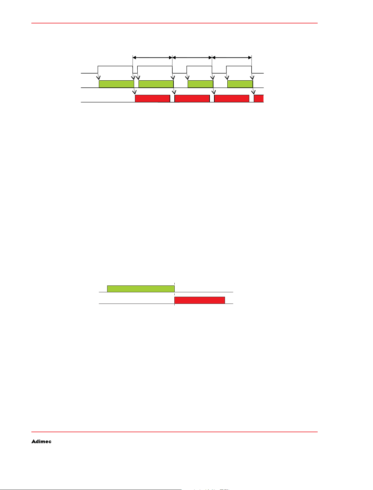
IMAGE CAPTURING AND VIDEO OUTPUT
OPERATING AND USER MANUAL OPAL-FAMILY
Exposure
control
Sensor
integration
Image
output
Minimal:
t_frame_min
Int. im 1 Int. im 2
Timing details normal control mode showing integration and image output overlap.Figure 7.1:
Output im 1
Minimal:
t_frame_min
Output im 2
t_frame_min
Int. im 3 Int. im 4
Minimal:
Output im 3
After image 1 has been acquired, it is send to the output due to the falling edge of exposure control.
While outputting image 1, image 2 can be acquired, started by the rising edge of exposure control.
This sequence can run continuously when the exposure control pulse duration is in accordance with
t_frame_min. (Texposure equal or greater than t_frame_min).
NOTE: in the simplified timing diagrams in par 7.5 up to and including par 7.9 integration and
transmitting of only one image is presented. This is done in order to keep the diagrams simple. In
practice however, timing might be a little different because integration time of a frame may start while
the previous frame is still being output.
Image Aquisition in continuous mode7.5
In continuous mode the camera is fully free-running. No external control signal is needed.
NOTE: When an external control signal is applied, it is ignored. Image acquisition and output timing
is controlled by setting the parameters for integration time and frame period. Basically the camera
integrates during a period as set by the integration time command and outputs the image data
immediately after exposure time is expired.
Factory default the camera is set to this mode. Refer to figure 7.2 for a simplified basic timing diagram.
CCD Operation
Camera Output
Simplified example continuous modeFigure 7.2:
Integration image
Image read-out
By means of the MO0 command the camera will enter continuous mode. In this mode image
acquistion cannot be influenced by means of hardware signals. The camera determines its own timing,
conforming to the integration time and frame period parameters as set by the applicable commands:
Command syntax: ITx
Where x = integration time or exposure time in units of 10 μs.
Command syntax: FPx
Where x = frame period in units of 10 μs.
37
Page 38
OPERATING AND USER MANUAL OPAL-FAMILY38IMAGE CAPTURING AND VIDEO OUTPUT
Both parameters can be read back from the camera
Command syntax: IT?
Reply message: x
Where x = integration time or exposure time in units of 10 μs.
Command syntax: FP?
Reply message: x
Where x = frame period in units of 10 μs.
If invalid parameter values are entered the camera will ignore these and react, depending on the
parameter error according to tabel 7.4.
PARAMETER ERROR CAMERA BEHAVIOR
frame period shorter than allowed (*) frame period will be programmed as fast as possible
frame period out of range 0..32000 command will be ignored
integration time longer than allowed (**) integration time will be programmed at its maximum
integration time period out of range 0..32000 command will be ignored
Camera behavior in case of an invalid parameterTable 7.4:
(*) The minimum frame period depends on camera model and on image format. See the paragraph about image
format (chapter 8) for detailed information
(**) The maximum integration time is a little bit shorter than the frame period. The minimum integration time and
maximum integration time in continuous mode can be found in table 7.5.
CAMERA MODEL MINIMUM INTEGRATION TIME MAXIMUM INTEGRATION TIME
OPAL-1000
OPAL-1600
OPAL-2000
OPAL-4000
OPAL-8000
Maximum integration time related to camera modelTable 7.5:
10 μs 320000 μs
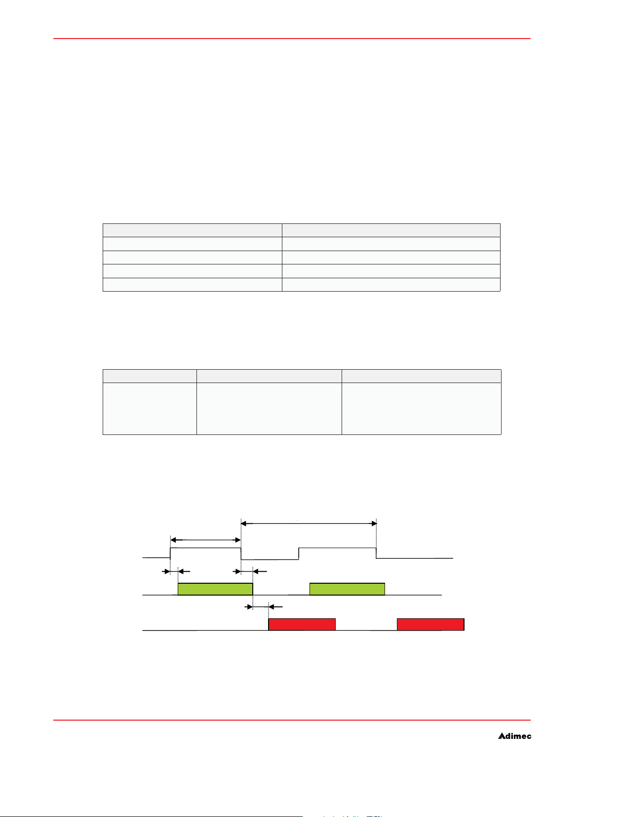
NOTE: The camera will not respond to external hardware trigger signals, the image acquiring system
(frame grabber) must be able to act as slave.For timing details see figure below. See table 7.2 & 7.3 for
the values of all timing parameters.
FP
IT
timing set by
parameters
td_it_bgn td_it_end
Image
Exposure
Image
output
Timing details continuous mode.Figure 7.3:
exposure exposure
td_output
Output image
Output image
Page 39
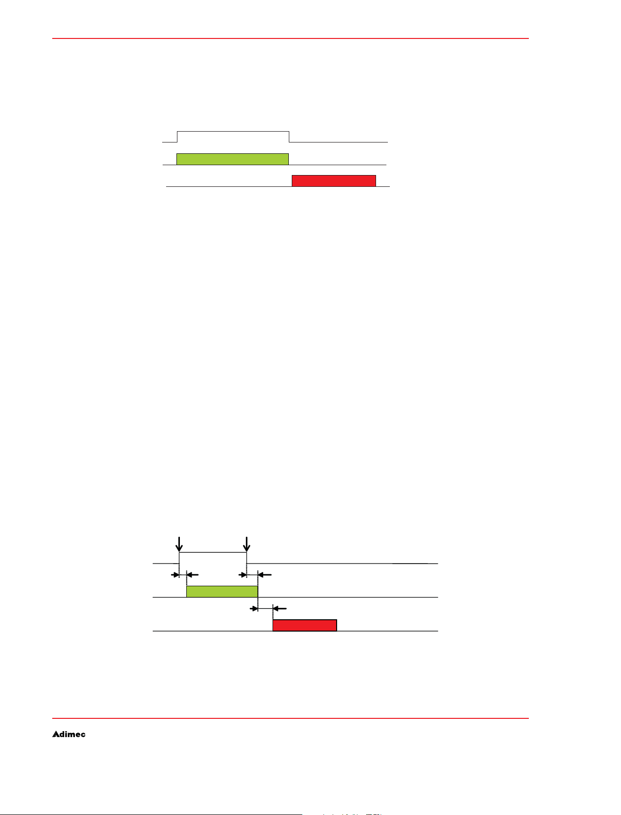
IMAGE CAPTURING AND VIDEO OUTPUT
Image Aquisition in normal control mode7.6
In normal control mode camera timing is controlled by means of an external signal. The parameters
for integration time and frame period can still be set and read-out but have no meaning. Refer to
figure 7.4 for a simplified basic timing diagram.
Control Signal
CCD Operation
Camera Output
Simplified example normal control modeFigure 7.4:
The image integration starts at a rising edge of the trigger signal. Image integration stops at the falling
edge. Image read-out starts at the falling edge of the same trigger control signal.
Controlling the camera timing by means of (an) external signal(s) is possible by means of several
(combinations of) signals. The selection and behavior of the control signals are explained in detail in
par. 7.10 and 7.11. To simplify explanations in this chapter we will assume that image integration and
image read-out are controlled by only one external signal, i.e. the Camera Control signal #1 in the
Camera Link interface, referred to as CC1.
The rising edge of CC1 is interpreted as a “start integrating” request; the falling edge is interpreted as
both a “stop integrating” and a “start sending image data” request.
Integration image
OPERATING AND USER MANUAL OPAL-FAMILY
Image read-out
Taking into account the remarks and descriptions as mentioned in par 7.1, one can conclude the
following restrictions on the trigger signal:
The time between two falling edges of the read-out trigger signal must be equal or longer than the •
minimum frame period valid for the image format programmed.
If a falling edge is detected too early, i.e. before the image is completely read out, then this event
is ignored.
To make use of the maximum speed possibilities of the camera it is generally necessary to •
generate a rising edge of the trigger signal before the previous image is completely read out.
If the integration time needs to be varied while grabbing images continuously, make sure that the
control signal edge corresponding with start-of-integration is varied. In standard settings this is the
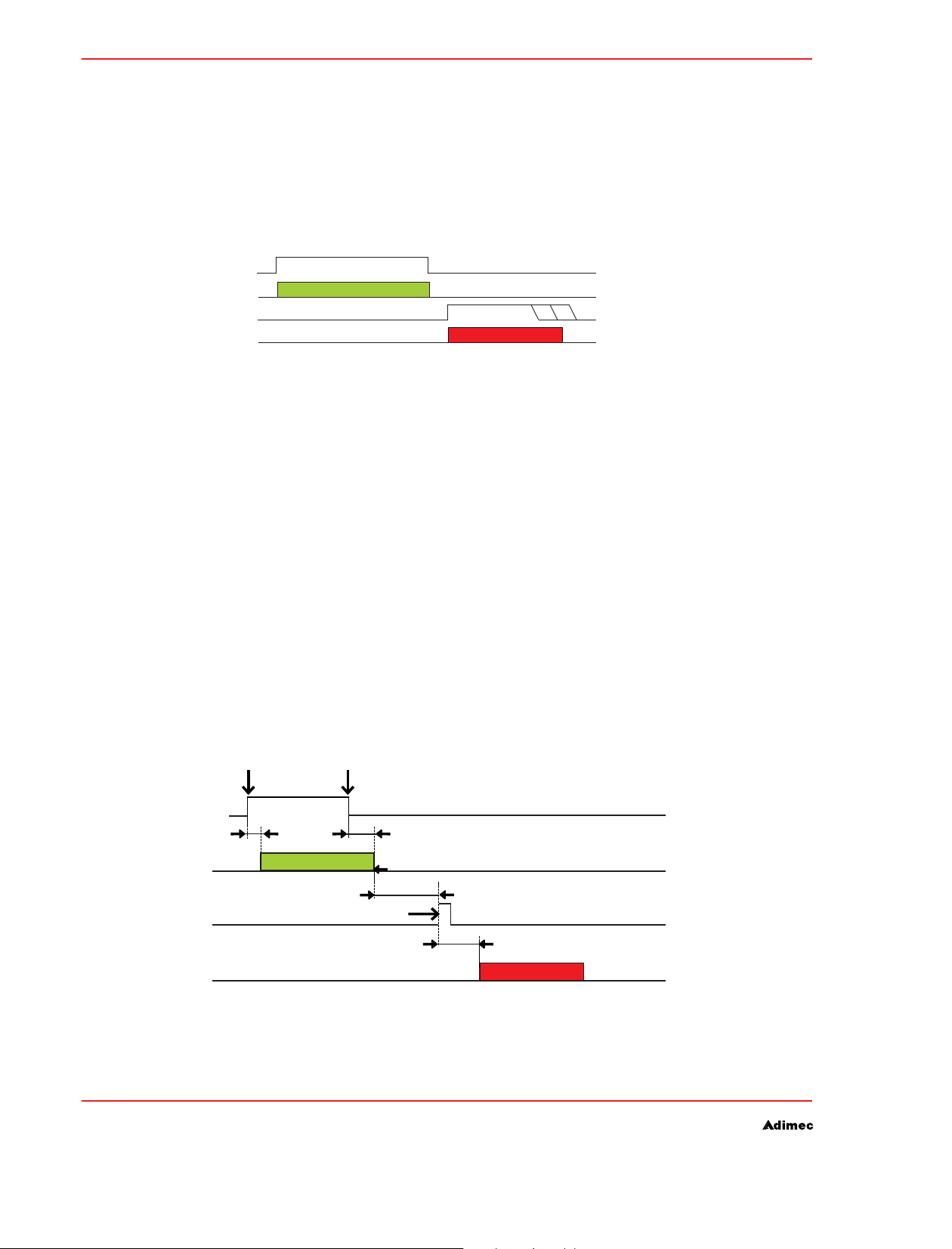
rising edge of the control signal. The falling edges of this signal must remain at constant timedistances in order to prevent a too early “start sending image data” request. For timing details see
figure 7.5. See table 7.2 & 7.3 for the values of all timing parameters.
Exposure
control
Sensor
integration
Image
output
Exposure
Start event
exposure
td_it_bgn td_it_end
Exposure
End event
integrating
td_output
Output image
Timing details normal control mode.Figure 7.5:
39
Page 40
OPERATING AND USER MANUAL OPAL-FAMILY40IMAGE CAPTURING AND VIDEO OUTPUT
NOTE: The selection and behavior of the control signals are explained in detail in par. 7.11 and 7.12.
Image Acquisition in delayed transfer mode (optional)7.7
In delayed transfer mode camera timing is controlled by means of two external signals. The
parameters for integration time and frame period can still be set and read-out but have no meaning.
Refer to figure 7.6 for a simplified basic timing diagram.
Control Signal #1
CCD Operation
Control Signal #2
Camera Output
Delayed transfer modeFigure 7.6:
The image integration starts at a rising edge of the trigger signal. Image integration stops at the falling
edge. Image read-out starts at the falling edge of another trigger control signal.
To simplify explanations in this chapter we will assume that image integration and image read-out are
controlled by CC1. The rising edge of CC1 is interpreted as a “start integrating” request; the falling
edge is interpreted as a “stop integrating” request. The rising edge of CC2 is interpreted as a “start
sending image data” request. The behavior of CC1 and CC2 is determined by the settings explained in
par. 7.11 and 7.12.
Integration image
Image read-out
Taking into account the remarks and descriptions mentioned in par 7.1, one can conclude the
following restrictions on the trigger signal:
The time between two falling edges of the read-out trigger signal must be equal or longer than the •
minimum frame period valid for the image format programmed.
If a falling edge is detected too early, i.e. before the image is completely read out, then this event
is ignored.
To make use of the maximum speed possibilities of the camera it is generally necessary to •
generate a rising edge of the trigger signal before the previous image is completely read out.
For timing details see figure 7.7. See table 7.2 & 7.3 for the values of all timing parameters.
Exposure
End event
td_it_bgn
integrating
Frame start event
td_it_end
Frame delay (see text)
td_output
Output image
Exposure
control
Sensor
integration
Frame
start
Image
output
Exposure
Start event
exposure
Timing details delayed transfer mode.Figure 7.7:
Page 41
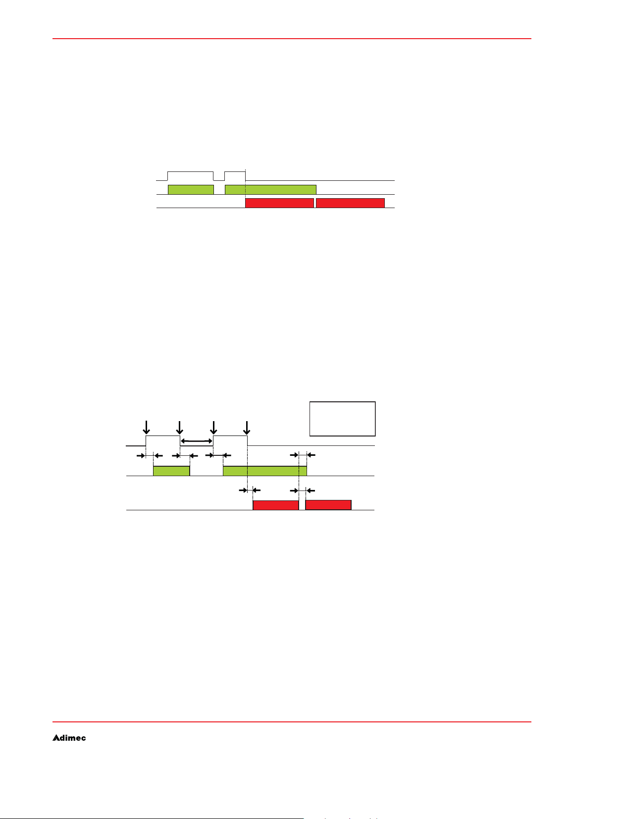
IMAGE CAPTURING AND VIDEO OUTPUT
NOTE: The selection and behavior of the control signals are explained in detail in par. 7.11 and 7.12.
Image Acquisition in double transfer mode (optional)7.8
Double transfer mode allows for the capture of two images shortly after each other. Image readout of
both images is postponed until integration of the second image is completed. Refer to figure 7.8 for a
simplified basic timing diagram.
OPERATING AND USER MANUAL OPAL-FAMILY
Control Signal
CCD Operation
Camera Output
Simplified example doube transfer modeFigure 7.8:
Integr. im. 1 Integr. im. 2
Im. 1 read-out Im. 2 read-out
In double transfer mode image acquisition is fully controlled by an external trigger input. Basically
operation is the same as normal control mode, except for the important difference that a captured
image will not always be output immediateley, thereby enabling the possibilitiy to capture a second
image immediately after the first one.
This feature can be extremely useful if the average number of required frames per second is within
normal camera capabilities, but when pairs of images must be captured on a much faster base.
General timing constraints are difficult to state, because they are completely dependent on the
application.
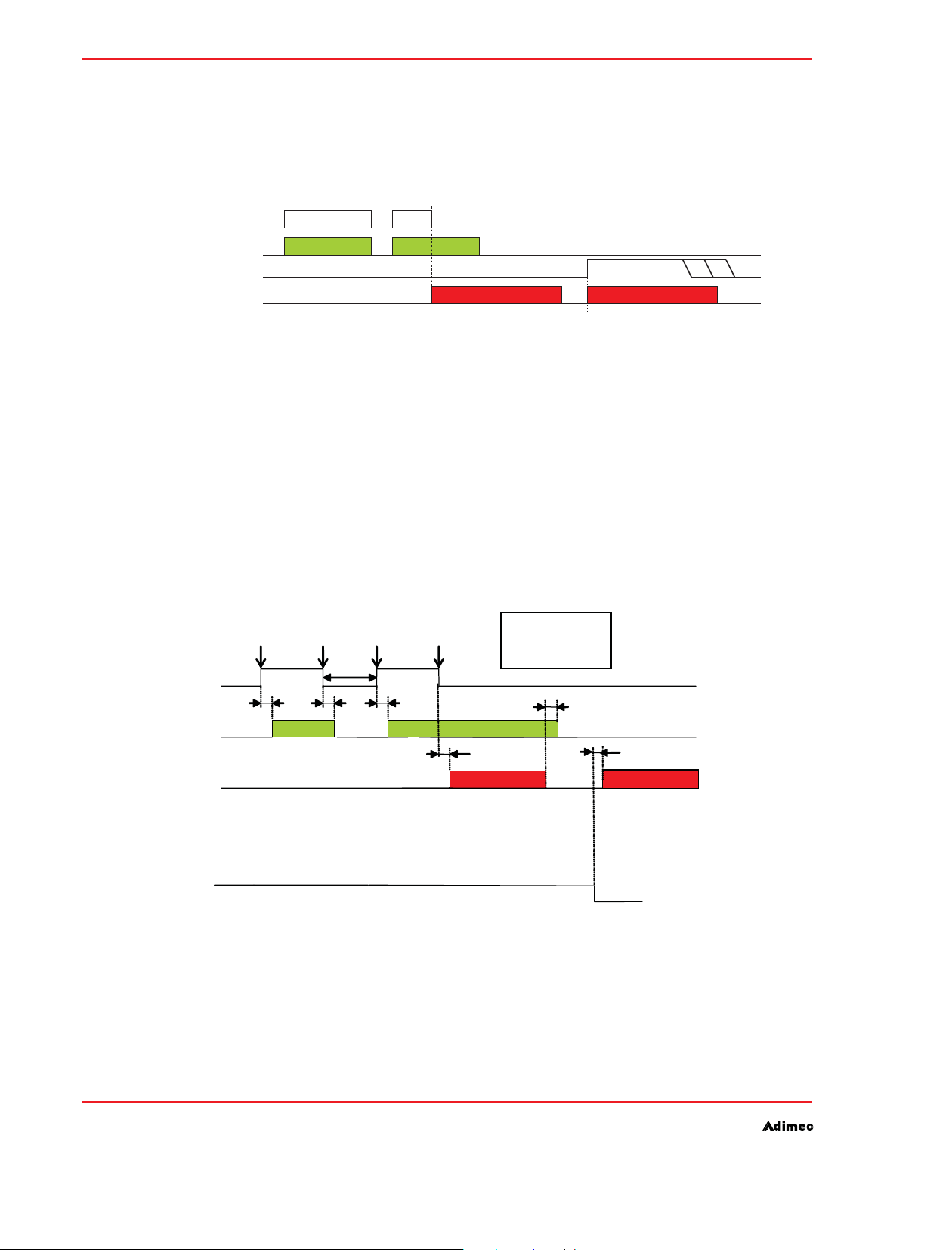
In general the constraints applicable can be derived from the timing diagram shown in figure 7.9.
See table 7.2 & 7.3 for the values of all timing parameters.
CC1
Sensor
integration
Image
output
Exp 1
Start
Exp 1
End
Exp. 1
t1
Int. lm1
Timing details double transfer mode.Figure 7.9:
Exp 2
Start
t3
t2
Exp. 2
Int. Im2
t1
Exp 2
End
td_output
Output im1
t1= td_it_bgn
t2= td_it_end
t3= t_dtm_gapmin
t2
td_output
Output im2
NOTE: The selection and behavior of the control signals are explained in detail in par. 7.11 and 7.12.
41
Page 42
OPERATING AND USER MANUAL OPAL-FAMILY42IMAGE CAPTURING AND VIDEO OUTPUT
Image Acquisition in double delayed transfer mode (optional)7.9
Double delayed transfer mode also allows for the capture of two images shortly after each other.
Image readout of both images is postponed until integration of the second image is completed.
Image readout of the second frame is controlled by a separate control signal. Refer to figure 7.5 for a
simplified basic timing diagram.
Control Signal #1
CCD Operation
Control Signal #2
Camera Output
Simplified example double delayed transfer mode.Figure 7.10:
In double delayed transfer mode image acquisition is fully controlled by two external trigger inputs.
Basically operation is the same as double transfer mode, except for the important difference that the
frame readout of the 2nd image is controlled by an additional external control signal. Note that frame
readout of the first images is still controlled by the same signal that controls the exposure.
This mode is useful at the same conditions as double transfer mode. In double transfer mode the
second image is generated immediately after the first one. If the host system (frame-grabber) is not
able to capture the second image directly after the first one, the double delayed transfer mode makes
it possible to delay the second image. General timing constraints are difficult to state, because they
are completely dependent on the application. In general the constraints applicable can be derived
from the timing diagram shown in figure 7.11.
Integr. im. 1 Integr. im. 2
Im. 1 read-out
Im. 2 read-out
See table 7.2 & 7.3 for the values of all timing parameters.
Exp2
Start
t3
Exp. 2
t1
Int. Im2
Exp2
End
t1
t2
t3
td_output
Output im1
= td_it_bgn
= td_it_end
= t_dtm_gapmin
t2
td_output
Output im2
CC1
sensor
integration
Image
output
CC2
Exp1
Start
Timing details double delayed timing mode.Figure 7.11:
Exp1
End
Exp. 1
t1 t2
Int. Im1
NOTE: The selection and behavior of the control signals are explained in detail in par. 7.11 and 7.12.
Page 43
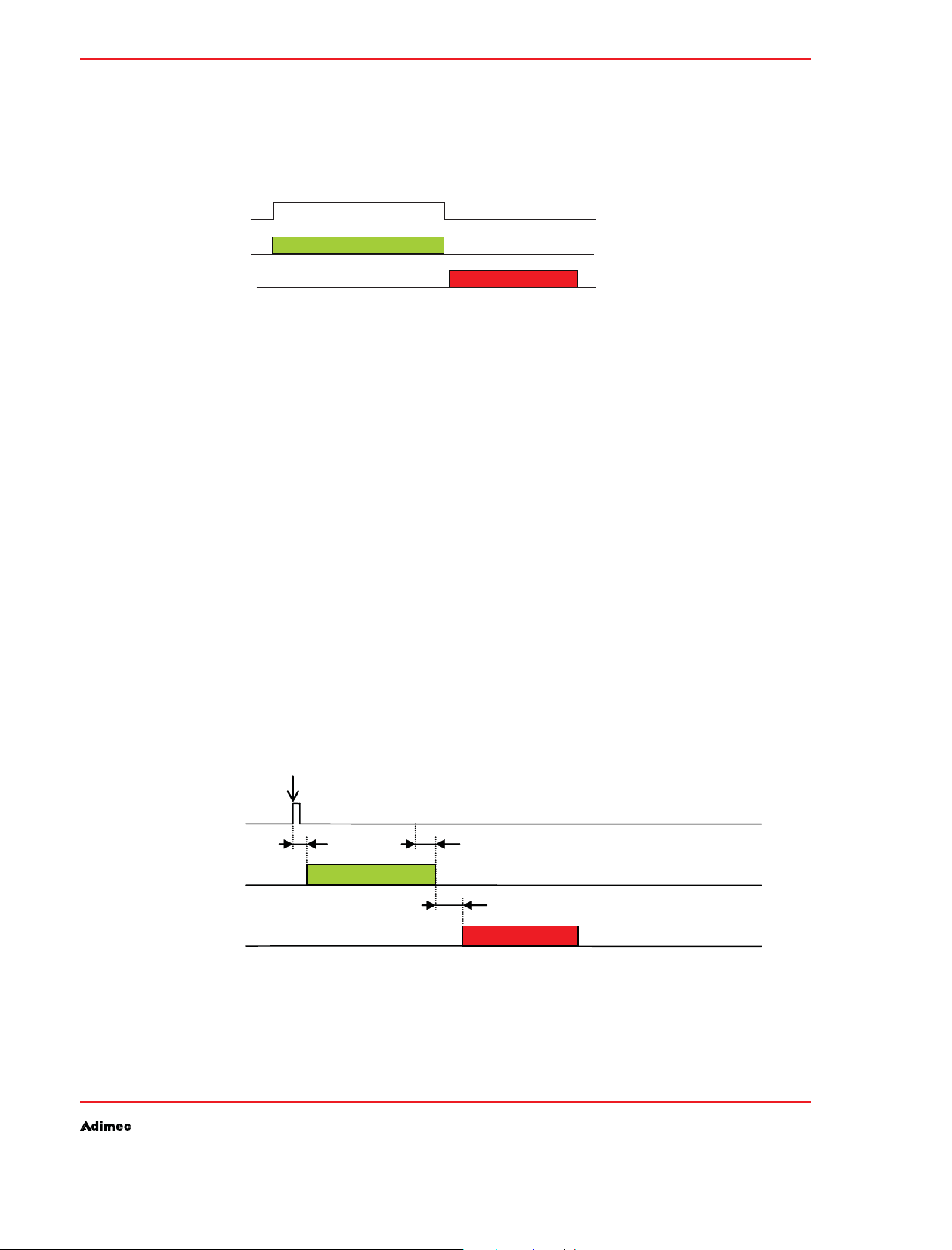
IMAGE CAPTURING AND VIDEO OUTPUT
Image Aquisition in IT defined integration control mode (optional)7.10
In IT defined integration control mode the start of integration is controlled by means of an external
signal. The parameters for integration time IT can be set to determine the integration time. Refer to
figure 7.11 for a simplified basic timing diagram.
Control Signal
CCD Operation
Camera Output
Simplified example normal control modeFigure 7.12:
The image integration starts at a rising edge of the trigger signal. Image integration stops after the set
integration time has passed. Image read-out starts as soon as integration has finished..
Controlling the start of integration by means of an external signal is possible by choise of several
control signals. The selection and behavior of the control signals are explained in detail in par. 7.11
and 7.12. To simplify explanations in this chapter we will assume that image integration start is
controlled by only one external signal, i.e. the Camera Control signal #1 in the Camera Link interface,
referred to as CC1.
The rising edge of CC1 is interpreted as a “start integrating” request; After the set integration time has
passed, the image is transmitted at the output.
Integration image
OPERATING AND USER MANUAL OPAL-FAMILY
Image read-out
Taking into account the remarks and descriptions as mentioned in par 7.1, one can conclude the
following restrictions on the trigger signal:
The time between two rising edges of the ‘start aqcuisition’ trigger signal must be equal or longer •
than the minimum frame period and set integration time valid for the image format programmed.
If a rising edge is detected too early, i.e. before the set integration time has passed, then this
event is ignored.
To make use of the maximum speed possibilities of the camera it is generally necessary to •
generate a rising edge of the trigger signal before the previous image is completely read out.
For timing details see figure 7.13. See table 7.2 & 7.3 for the values of all timing parameters.
Exposure
control
Sensor
integration
Image
output
Normal control mode, IT defines integration timeFigure 7.13:
Exposure
Start event
td_it_bgn
integrating
Exposure IT
td_it_end
td_output
Output image
43
Page 44
OPERATING AND USER MANUAL OPAL-FAMILY44IMAGE CAPTURING AND VIDEO OUTPUT
Polarity and choice of external triggers7.11
Introduction7.11.1.
Controlling integration and read-out in each one of the control inputs can be done by every one of the
CC1..CC4 and/or the external trigger input on the I/O-connector. Which control signals control which
event is fully programmable.
It is also possible to change the polarity of each one of the trigger signals.
Exposure control7.11.2.
Exposure control is done by means of the Camera Control Exposure command. This is applicable in
the following modes:
Normal control mode•
Delayed transfer control mode•
Double transfer control mode•
Double delayed transfer control mode•
Command structure: CCEe;f
Where e and f are defined in the table below
The actual camera control event setting can be read back from the camera
Command syntax: CCE?
Reply message: e;f
Where e and f are defined in the table below
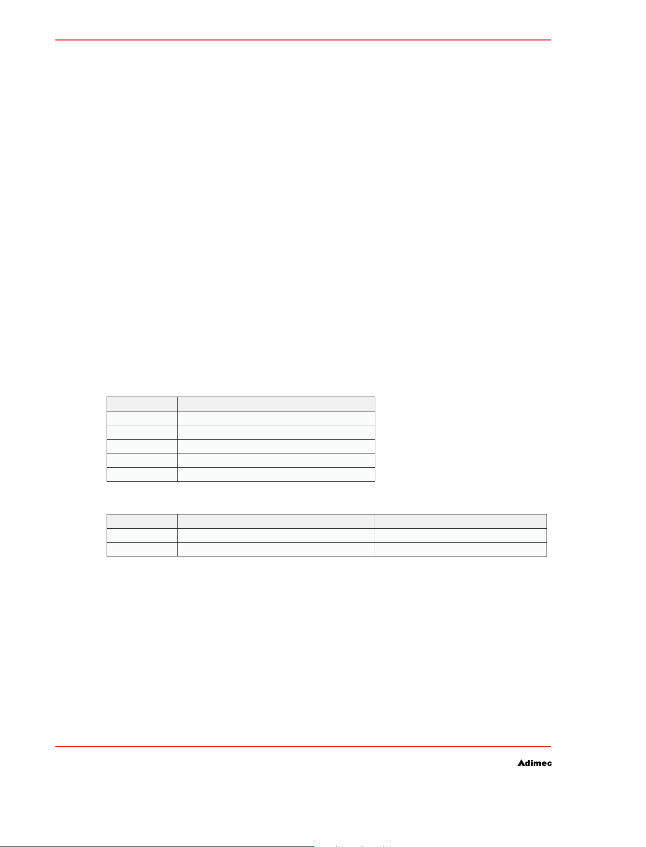
E Trigger input signal source
0 CC1
1 CC2
2 CC3
3 CC4
4 I/O-connector
Exposure control trigger source selectionTable 7.6:
F RISING EDGE IS INTERPRETED AS FALLING EDGE IS INTERPRETED AS
0 End of integration Start of integration;
1 Start of integration End of integration
Polarity selectionTable 7.7:
Page 45
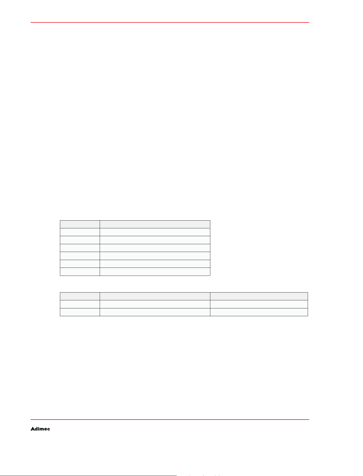
IMAGE CAPTURING AND VIDEO OUTPUT
Read-out control7.12
Exposure control is done by means of the Camera Control Exposure and Camera Control Frame
read-out.
Read-out control is done by means of the Camera Control Frame readout command. This is applicable
in the following modes:
Delayed transfer control mode•
Double delayed transfer control mode•
NOTE: In Normal control mode and in Double transfer control mode image readout always starts at the
end of exposure. There is no separate camera read-out trigger signal and the Camera Control Frame
readout command is therefore not applicable.
Additional to starting read-out with an external trigger signal, it is also possible to start readout upon
a ‘soft request’. This is a request done by a separate command. This possibility is programmed by
means of the same Camera Control Frame readout command.
Command structure: CCFSg;h
Where g and h are defined in the table below. The actual camera control event setting can be read
back from the camera
OPERATING AND USER MANUAL OPAL-FAMILY
Command syntax: CCFS?
Reply message: g;h
Where g and h are defined in the table below.
G CORRESPONDING SOURCE
0 CC1
1 CC2
2 CC3
3 CC4
4 Trigger input signal on I/O-connector
5 Soft request
frame readout trigger source selectionTable 7.8:
H RISING EDGE IS INTERPRETED AS FALLING EDGE IS INTERPRETED AS
0 Start of readout
1 Start of readout
Polarity selectionTable 7.9:
This command triggers the readout of the acquired image.
Command syntax: RQ
NOTE: On soft request, if frame read-out trigger source is set to Soft request, then the frame readout
is not initiated by an external signal, but by the additional Camera Control Request frame command
45
Page 46

OPERATING AND USER MANUAL OPAL-FAMILY46IMAGE CAPTURING AND VIDEO OUTPUT
Flash strobe7.13
Flash strobe enable7.13.1.
The camera is equipped with strobe output signal on the I/O connector. The strobe can be switched on
off by means of the FSE command.
Command syntax: FSEx
Where x is set to 0 to disable the strobe output and x is set to 1 to enable the strobe output. The
definition of the active state depends on the strobe polarity.
The actual setting can be read back from the camera.
Flash strobe polarity7.13.2.
The active state of the strobe output can be inverted to adapt to the application requirements.
Command syntax: FSPx
Where x is set to 0 for the reverse polarity: in this polarity configuration the phototransistor at the
camera output is non-conductive during the active state of the strobe.
And x is set to 1 for the normal polarity: in this polarity configuration the phototransistor at the camera
output is conductive during the active state of the strobe.
The actual setting can be read back from the camera.
Flash strobe mode7.13.3.
The strobe output can be operated in two different modes, which are set through the FSM command.
Command syntax: FSMx
Where x is set to 0 for the automatic mode: The strobe will become active at the start of integration.
The strobe will deactivate when the acquisition is completed.
If x is set to 1 the strobe will operate in programmed mode; both delay time after a sensor reset as well
as the duration of the active state can be programmed. A new flash window can only start after the
completion of the previous flash strobe window.
The actual setting can be read back from the camera.
Flash strobe Timing7.13.4.
The strobe output timing can be programmed through the FST command.
Command syntax: FSTx;y
Where x indicates the delay time between the sensor reset operation and the active state of
the strobe.
Where y indicates the duration of the strobe if the camera is in programmed strobe timing
mode. Note the parameters are ignored in automatic strobe mode.
Valid ranges for both x and y are 0 … 32000. Both x- and y-values are in units of 10 μs.
The actual settings can be read back from the camera.
Page 47

IMAGE AND DATA FORMATTING
Image and Data Formatting8.
Introduction8.1
Although the CCD in the camera has a fixed format there are several possibilities to change the way
the CCD is read-out. It is possible to limit the amount of lines read from the CCD (discussed in par
8.2); it is also possible to change the readout-direction (discussed in par. 8.7).
The video-processing, which converts the analog CCD-signal to the digital Camera Link output can
also be changed. It is possible to choose the number of bits on the output (discussed in par. 8.6, it is
possible to program a digital gain (discussed in par. 8.8) and there is a possibility to change the output
offset. For color camera models it is possible to program additional gains for the R- G- and B-pixels in
color camera models.
All cameras have a factory set defect pixel correction. Enabling / disabling this correction can be
selected by the user. The user is able to add defect pixels to and remove defect pixels from the defect
pixel table. A defect pixel mask can be made visible to the user.
Binning8.2
Settings8.2.1.
In certain circumstances it might be preferable to sum 2 or more pixels. In CCD terms this process
is called binning. If two or more pixels are binned the combination of those pixels can be regarded
as one larger “bin-pixel”. In which circumstances this is preferable can be determined if the
consequenses of binning are known.
OPERATING AND USER MANUAL OPAL FAMILY
A typical CCD implementation of this mechanism is to bin 2 pixels vertically. This is referred to as
vertical binning and can be done on the CCD chip. This is the only binning feature that is available
on a standard OPAL camera. Theoretically more pixels vertically can be binned and even horizontal
binning is theoretically possible, the latter is discussed later.
One important property of on-chip binning is that it takes less time to read all the data out of the chip.
As a consequence the maximum framespeed rises, this is regarded as the most important advantage.
Another consequence is that there is less data on the CameraLink output to process.
Another consequense is that at N times binning the sensitivity of the camera increases with a factor of
N at the cost of a decrease in resolution by a factor of N.
At the camera output Full Scale will always correspond with a Qmax of 18kel. Note that at 2x binning
this corresponds with 18 kel in the “bin-pixel” or 9 kel per normal pixel.
OPTIONAL: Optionally 4 and 8 times vertical binning and horizontal binning is available. The following
only refers to cameras with these non-standard options in place.
For 4x and 8x vertical binning goes that sensitivity increases with a factor of 4 and 8. The maximum
possible framespeed also increases
Horizontal binning cannot be done on the CCD. This type of binning is done electronically, referred to
as off-chip. This enables the possibility to correct for the increasing sensitivity. In the OPAL camera
this is done automatically and can not be switched off. So when changing from no horizontal binning
to 2x horizontal binning image brightness will not alter.
Horizontal binning gives no speed advantage; it does give the advantage of having less data on the
CameraLink interface.
47
Page 48

OPERATING AND USER MANUAL OPAL FAMILY
For a thorough understanding of the concept please find some properties of the possibilities (including
optional binning modes) in the diagram below.
The standard OPAL camera only offers two binning modes: no binning (1x) and 2x vertical binning.
IMAGE AND DATA FORMATTING
HBIN
FACTOR
1 1 5.5 x 5.5 18 18 1 x
1 2 5.5 x 11 18 9 2 x
1 4 * 5.5 x 22 18 4.5 4 x
1 8 * 5.5 x 44 18 2.25 8 x
2 * 1 * 11 x 5.5 36 18 1 x
2 * 2* 11 x 11 36 9 2 x
(*: optional only; not available on a standard camera)
VBIN
FACTOR
Theoretical charge values of camera in binning modes.Table 8.1:
“BIN
PIXEL”
SIZE (H*V)
[MICONS]
BIN PIXEL CHARGE
CORRESPONDING WITH
FULL SCALE CAMERA OUTPUT [KEL]
PIXEL CHARGE
CORRESPONDING WITH
FULL SCALE CAMERA OUTPUT [KEL]
SENSITIVITY,
RELATIVE TO
BINNING FACTOR
NOTE: There are particular drawbacks in vertical binning. These will be discussed in par 8.2.3.
Vertical binning mode is set by means of the VBIN command.
Command syntax: VBINy
where
y=0 denotes no binning
y=1 denotes binning enabled; two vertical pixels are added
y=2 denotes binning enabled; four vertical pixels are added (OPTIONAL)
y=3 denotes binning enabled; eight vertical pixels are added (OPTIONAL)
The actual binning mode can be read back from the camera
Command syntax: VBIN?
Reply message: y
where
y = as above
Horizontal binning mode is set by means of the HBIN command.
Command syntax: HBINx (OPTIONAL)
where
x=0 denotes binning off
x=1 denotes binning on; two horizontal pixels are binned (not available on the standard camera)
The actual binning mode can be read back from the camera
Command syntax: HBIN? (OPTIONAL)
Reply message: x
where
x = as above
Binning is not available on a color camera because binning neighboring pixels would make the Bayer
color pattern useless.
48
Page 49

IMAGE AND DATA FORMATTING
Frame rate consequences when vertical binning is used8.2.2.
If the vertical binning is used, the maximum possible frame rate will be higher than the standard frame
rate. The camera will however not automatically increase frame rate when binning is enabled.
If the vertical binning is disabled or is switched to a lower binning factor, then the maximum possible
frame rate decreases. If the camera is running in control mode, make sure to check if the external
trigger signal complies with the new maximum frame rate.
If the camera is running in continuous mode, the frame rate is automatically decreased if necessary
when vertical binning is disabled or switched to a lower binning factor.
When a higher binning factor is selected, the frame rate is not automatically increased! The maximum
frame rate depends on the vertical resolution which is different for camera model, according to the
table below.
OPERATING AND USER MANUAL OPAL FAMILY
CAMERA
MODEL
OPAL-1000m 123
OPAL-1600m 69 fps 1600x1200 127
OPAL-2000m 65 fps 1920x1080 121
OPAL-4000m 33 fps 2336x1752 59 fps 2336x876 97 fps 2336x438 142 fps 2336x219
OPAL-8000m 17 fps 3296x2472 32 fps 3296x1236 55 fps 3296x618 85 fps 3296x309
NO BINNING 2X VBINNING 4 X VBINNING* 8X VBINNING*
fps
OUTPUT
FRAME
H*V
1024x1024 215
fps
fps
fps
OUTPUT
FRAME
H*V
1024x512 346
fps
1600x600 216
fps
1920x540 210
fps
OUTPUT
FRAME
H*V
1024x256 492 fps 1024x128
1600x300 333 fps 1600x150
1920x270 330 fps 1920x135
FRAME
RATE
OUTPUT
FRAME
H*V
* optional
Relation between vertical binning and maximum framerate.Table 8.2:
Image quality considerations when binning is used8.2.3.
The electronics in the camera are optimized in order to detract as little as possible from any image
artifact or image quality degradation when vertical binning is used. There are some principle
drawbacks due to CCD properties.
The best way to illustrate this is to regard the binned CCD as a sensor with image pixels doubled in
size in the vertical direction. The sensitivity of the camera will increase, due to the larger pixel. The
capacity of the photo-pixel is also doubled. The capacity of the transfer register remains the same,
but is large enough to transport the charge of two pixels. When binning more than two pixels (optional
feature to the standard camera), transport capacity is not enough for the full load of saturated pixels.
This may lead to excessive blooming when using binning, although the image was distortion-free in
non-binning mode.
Also note that noise level will approximately remain the same. Because sensitivity, increases the
signal-to-noise ratio seems to increase. But bear in mind that the signal will saturate at half the level
that the camera would saturate in a non-binning format.
The output image resolution will decrease by the applied factor of binning.
Summarized: the dynamic range of the camera in binning format is approximately the same as in
non-binning format. In fact the dynamic range is a little bit smaller, because noise does increase a
small amount.
49
Page 50
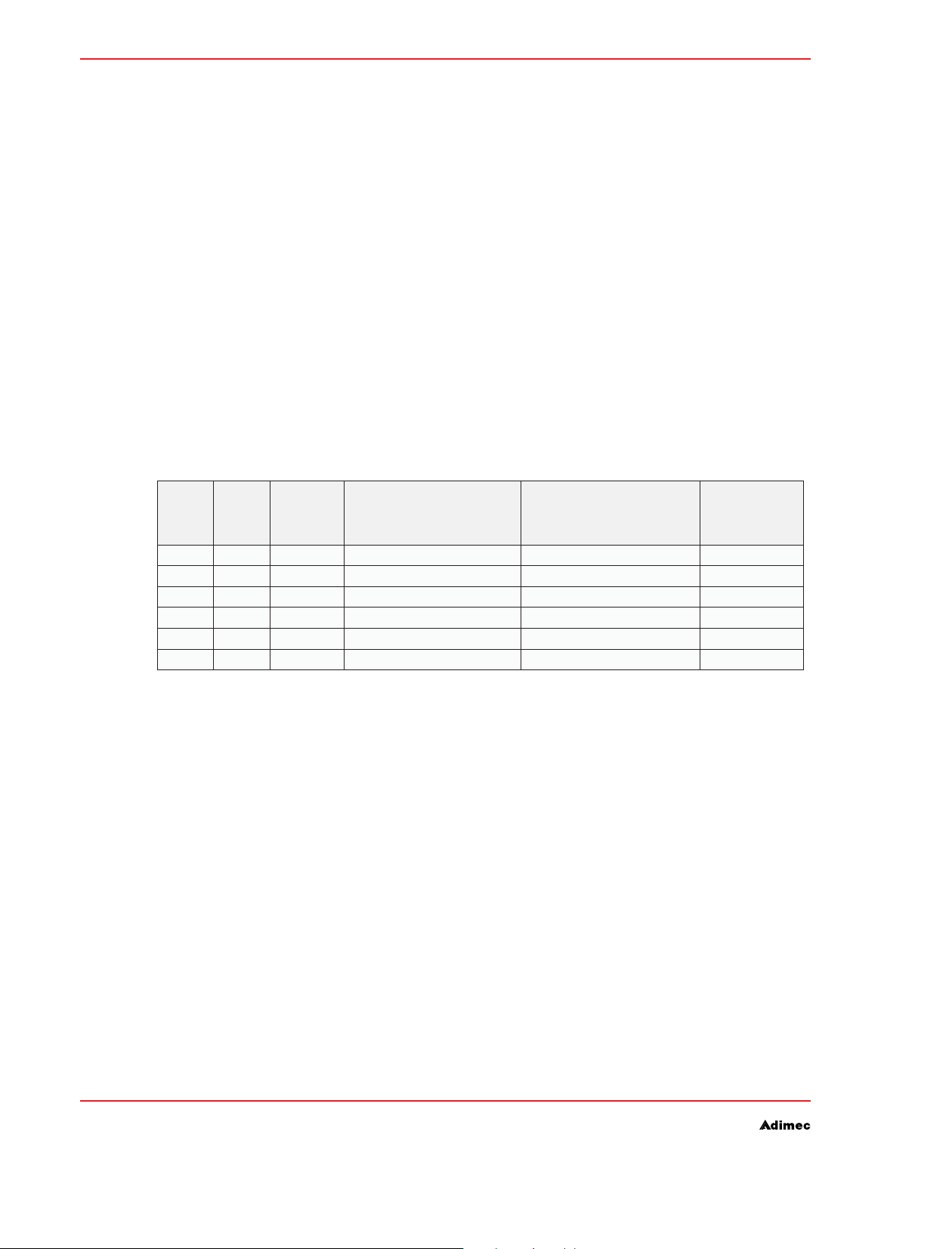
OPERATING AND USER MANUAL OPAL FAMILY
Binning without sensitivity consequences8.2.4.
OPTIONAL: A special non-standard feature is the Hi-Qmax option. If this option is ordered the
electronic gain in the camera will be halved when two (or more when possible) lines are vertically
binned. The following text only applies to Hi-Qmax cameras.
This option makes the sensitivity of the camera independent from the choice 1x or 2x vertical binning;
the theoretical Qmax however does alter depending on binning settings.
Combining the Hi-Qmax option with the optional 4x and 8x vertical binning and horizontal binning
leads to the following behaviour: All choices consisting of 1x or 2x horizontal binning and 1x or 2x
vertical binning have the same sensitivity. Sensitivity does increase when 4x or 8x binning is selected;
gain at these settings is not adapted, but fixed at the 2x binning value.
It is important to realize that the Hi-Qmax option does not solve any of the artifacts from par. 8.2.3.
Excessive CCD charge will still lead to blooming effects, which tend to be more visible in a Hi-Qmax
camera than in a standard camera. The Hi-Qmax option is therefore only deliverable on special
request. The Hi-Qmax option is not swichable. A camera ordered with the Hi-Qmax option will always
have the Hi-Qmax behaviour. The Hi-Qmax camera will not behave according to table 8.1, but to the
following table. Note that the charge values are theoretical values. Charges much larger than twice the
photo-pixel capacity of 18kel are in practise not transportable, so either not realizable or will result in
excessive blooming.
IMAGE AND DATA FORMATTING
HBIN
FACTOR
1 1 5 x 5 18 18 1 x
1 2 5 x 10 36 18 1 x
1 4* 5 x 20 36 9 2 x
1 8* 5 x 40 36 4.5 4 x
2* 1 10 x 5 36 18 1 x
2* 2 10 x 10 72 18 1 x
VBIN
FACTOR
“BIN
PIXEL”
SIZE (H*V)
[MICONS]
BIN PIXEL CHARGE
CORRESPONDING WITH
FULL SCALE CAMERA OUTPUT [KEL]
PIXEL CHARGE
CORRESPONDING WITH
FULL SCALE CAMERA OUTPUT [KEL]
SENSITIVITY,
RELATIVE TO
NO BINNING
*optional
Theoretical charge values of Hi-Qmax camera in binning modesTable 8.3:
Region of Interest (optional)8.3
A Region of Interest can be selected in order to reduce the amount of data transmitted over Camera
Link; only the part of the image selected as ROI is output. Selecting a ROI does not increase the
framerate. This is due to the fact that even with a selected ROI, the sensor has to be read out
completely.
The Region of Interest can be set by the ROI command
Command syntax: ROIx;y;w;h
50
Where:
x = offset of the ROI relative to the left side of the image, range 0 to image width
y = offset of the ROI relative to the top of the image, range 0 to image height
w = width of the ROI, range 2 to image width
h = height of the ROI, range 2 to image height
Page 51
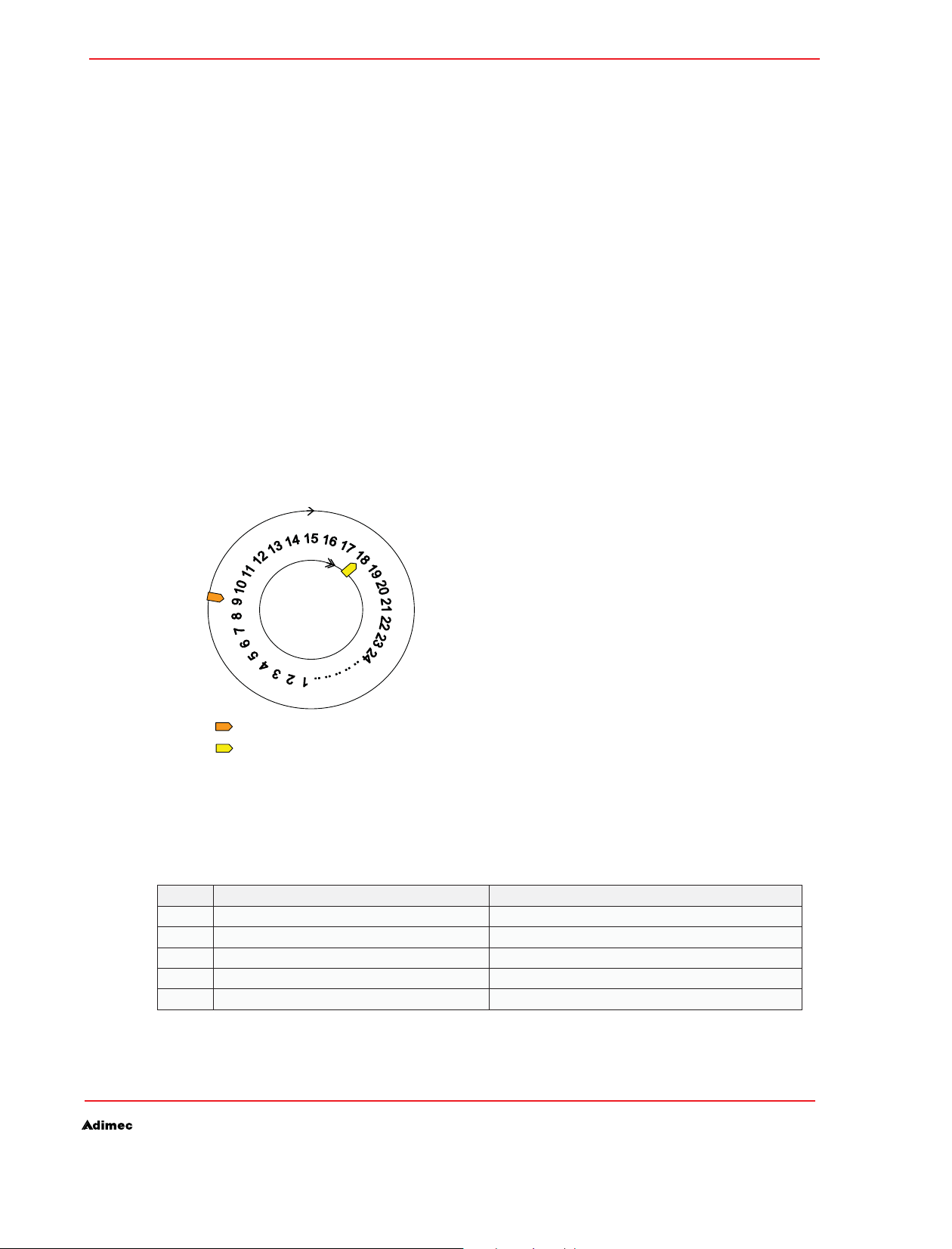
IMAGE AND DATA FORMATTING
Write images to memory
NOTE: Only even values are expected to be entered at the ROI command.
The actual Region of Interest can be read back from the camera.
Command syntax: ROI?
Reply message: x;y;w;h
Where x, y, w and h are representing the values as described above
NOTE: Selecting a Region of Interest can be performed together with Burst Mode. In doing so, the
amount of images stored im memory increases relative to full image Burst Mode.
NOTE: ROI0;0;max. image width;max. image height disables the selected ROI.
Burst mode (optional)8.4
The camera can be equipped with a ringbuffer memory. This memory can be used to temporarily delay
the output of the images when the camera is operated in control mode MO1. Acquisition and readout
are decoupled and may take place asynchronously when using Burst Mode. Not that Burst mode does
not increase the maximum framespeed, because the maximum frame speed is determined by sensor
characteristics. A predefined number of images in the buffer will be released at request.
OPERATING AND USER MANUAL OPAL FAMILY
Read images from memory
Circular representation of the ringbuffer memoryFigure 8.1:
The memory size is limited. Table 8.4 shows an overview of the number of images that can be stored
at full resolution. When using Region of Interest, the number of images increases, depending on the
size of the ROI.
OPAL # IMAGES @ 8 BIT OUTPUT RESOLUTION # IMAGES @ 10 & 12 BIT OUTPUT RESOLUTION
1000 128 64
1600 69 34
2000 64 32
4000 32 16
8000 16 8
Buffer capacity at full resolutionTable 8.4:
51
Page 52

OPERATING AND USER MANUAL OPAL FAMILY
To enable the Burst Mode the BMO command is available
Command syntax: BMOx
Where:
x = 0 for normal operation, disabling Burst Mode
x = 1 for Burst Mode with automatic image release. An image is output as soon as one complete
image is in the buffer memory.
x = 2 for Burst Mode with software triggered image release. On software request,
a defined number of images are released from the memory.
The burst mode can be obtained from the camera using the BMO? command
Command syntax: BMO?
Reply message: x
Where: x is the status of the Burst Mode as indicated above.
To set the number of images to be released from memory per request the RQSIZE command can be
used.
Command syntax: RQSIZEx
IMAGE AND DATA FORMATTING
Where x = 0 to 255
To check the set number of imges released on request use Command RQSIZE?
Command syntax: RQSIZE?
Reply message: x
Where: x is the number of images released on request.
To generate a request use command RQ.
Command syntax: RQ
Interpretation of RQ? differs for the several image acquisition modes. If the camera is in Control Mode
(MO1), RQ generates a soft event for Burst Mode, provided Burst Mode is set to 2. If the camera is
in one of the optional image acquisition modes 2, 3 or 4 (not standard available), RQ generates a soft
event for delay / double control mode. In all other combinations of image acquisition mode (MO) and
Burst Mode (BMO, the RQ command does not have a function.
The number of images present in the burst memory can be obtained by the BCNT? command.
Command syntax: BCNT?
Reply message: x
Where x represents the number of images.
In the case that the number of image acquired exceeds the number of free memory locations, the
Buffer Overrun flag is set and the BurstCount register is set to 0.
52
the Buffer overrun status can be obtained by the BO? command.
Command syntax: BO?
Reply message: x
Where x = 0 means no overrun and x = 1 Burst Mode memory overrun
Page 53
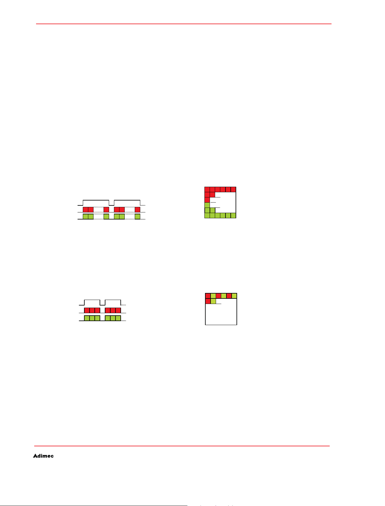
IMAGE AND DATA FORMATTING
Left Right
Left Righ
NOTE: In practice, the memory locations that already have been read out during acquisition are
available as free memory.
As an example; the OPAL-1000 has a memory capacity of 64 images of 12 bit resolution. Maximum
acuisition speed is 120 frames per second. When reading out the memory at 60 frames per second
during acquisition, the total number of 64 + 32 + 16 + 8 + 4 + 2 = 126 frames can be acquired before
memory overrun occurs.
When memory overrun has occurred, the burst memory can be flushed and the BO flag can be cleared
by the FB command.
Command syntax: FB
Vertical remap8.5
The camera is equipped with a four-tap CCD. Data is read from the top and the bottom of the CCD
simultaneously. For applications requiring minimum frame data delay, it might be advisable to operate
the camera with vertical remapping disabled. In that case top and a bottom pixel will be output
through the Camera Link Interface simultaneously. The top pixel will be at tap A and the bottom pixel
at tap B, provided vertical mirror is disabled. This is illustrated in figure 8.2 & 8.3 by means of a 36
pixel CCD ( 6 x 6)..
LVA L
Tap A
Tap B
1
2
31
7
6
25
36
OPERATING AND USER MANUAL OPAL FAMILY
Top
16
7
Output image
13
19
25
3631
Bottom
Output with vertical remap disabledFigure 8.2: Example 36 pixel CCDFigure 8.3:
For a more intuitive camera output it is possible to enable the vertical remap function. The data from
the CCD will be rearranged in order to provide normal left-to-right, top-to-bottom scanning. Note that
the Camera Link data will be delayed half a frame when compared with the no-remapping situation.
When remapping is enabled, neighboring odd and even pixels will be output simultaneously. The odd
pixels will be at tap A and the even pixels at tap B, provided the horizontal mirror is switched off.
To p
16
2543
8
LVA L
Tap A
Tap B
7
8
911
10
12
1
4356
2
Output with vertical remap enabled.Figure 8.4: Example readout direction.Figure 8.5:
7
Output image
Bottom
t
53
Page 54

OPERATING AND USER MANUAL OPAL FAMILY
Enabling and disabling the vertical remap is done by means of the vertical remap command.
Command syntax: VRx
Where:
x=0 denotes no vertical remapping; simultaneous output of top and bottom pixel, no delay.
x=1 denotes vertical remapping active; simultaneous output of even and odd pixel, half frame delay.
The actual vertical remap setting can be read back from the camera.
Command syntax: VR?
Reply message: x
Where x = 0 or 1 as above.
Output resolution8.6
The bit depth of the camera output can be set by the output resolution command.
Command syntax: ORx
Where x = 8, 10 or 12.
The actual output resolution can be read back from the camera.
IMAGE AND DATA FORMATTING
Command syntax: OR?
Reply message: x
Where x = 8, 10 or 12.
Mirror8.7
Depending on the application it can be necessary to have a horizontally or vertically mirrored output.
Changing the horizontal and/or vertical readout direction is done by means of the mirror command.
Command syntax: MIx
Where x = value accoding the mode in table 8.5
The actual mirror setting can be read back from the camera.
Command syntax: MI?
Reply message: x
Where x = value accoding the mode in table 8.5
X VERTICAL MIRROR HORIZONTAL MIRROR OUTPUT IMAGE
0- -
1- Yes
2Yes -
3Yes Yes
d
b
q
p
54
Mirror settingsTable 8.5:
Page 55

IMAGE AND DATA FORMATTING
NOTE: When changing the vertical mirror setting, the camera needs initializing of the hardware and
therefore will perform a soft-reboot. The camera will need up to 1 second to apply the new settings. A
short interruption of camera operation takes place when switching the ReverseY parameter. Changing
the vertical mirror on frame to frame base is not advised.
Digital gain8.8
A programmable amplifier enables you to apply gain in the signal path. Note that this is an electronic
gain, not influencing CCD operation. So sensitivity and noise are equally amplified, the saturation level
remains the same in terms of camera output. Saturation level will decrease in terms of light level when
gain increases.
Command syntax: GAx
Where x = 100..3200, representing a gain of 1.00x .. 32.00x
The actual gain setting can be read back from the camera.
Command syntax: GA?
Reply message: x
Where x = 100..3200, representing a gain of 1.00x .. 32.00x
OPERATING AND USER MANUAL OPAL FAMILY
White Balance (only for color)8.9
To correct for different illumination colors it is possible to program additional gain per color channel.
Command syntax: WBr;g;b
Where r = 100..399, representing a gain in the red channel of 1.00x .. 3.99x
g = 100..399, representing a gain in the green channel of 1.00x .. 3.99x
b = 100..399, representing a gain in the blue channel of 1.00x .. 3.99x
The actual white balance setting can be read back from the camera.
Command syntax: WB?
Reply message: r;g;b
Where r = 100..399, representing a gain in the red channel of 1.00x .. 3.99x
g = 100..399, representing a gain in the green channel of 1.00x .. 3.99x
b = 100..399, representing a gain in the blue channel of 1.00x .. 3.99x
NOTE: The total gain per color can not be greater that 32x. So the product of digital gain (par 8.8) and
white balance gain is clipped to 32x.
55
Page 56

OPERATING AND USER MANUAL OPAL FAMILY
Offset (only for color)8.10
In order to enable all captured information to be displayed within the digital domain an offset is applied
on the camera output data. Black is not represented by 0, but by the value programmed with the offset
command.
This ensures that all noise information, even when looking at absolute dark, is quantized and
reproduced on the output
Command syntax: OFSx
Where x = 0..4096, the offset in greylevels on a 12 bit scale.
The actual offset setting can be read back from the camera.
Command syntax: OFS?
Reply message: x
Where x = 0..4096, the offset in greylevels on a 12 bit scale.Note: the offset is defined at the camera
output on a 12 bit scale. That means that if the camera is switched to another output resolutions than
12 bit the actual offset seen on the output will be different.
Offset on Camera Output with an output resolution of 10 bit = x/4
Offset on Camera Output with an output resolution of 8 bit = x/16
See par 8.6 for information about output resolution and the the OR command
IMAGE AND DATA FORMATTING
For monochrome cameras the offset command is not available. Use the blacklevel command instead
to alter the output offset.
Blacklevel (only for monochrome)8.11
In order to enable all captured information to be displayed within the digital domain an offset is applied
on the camera output data. Black is not represented by 0, but by the value programmed with the offset
command.
This ensures that all noise information, even when looking at absolute dark, is quantized and
reproduced on the output.
Command syntax: BLx
Where x = 0..4096, the blacklevel in greylevels on a 12 bit scale, before the digital gain stage.
The actual blacklevel setting can be read back from the camera
Command syntax: BL?
Reply message: x
Where x = 0..4096, the black level in greylevels on a 12 bit scale before the digital gain stage.
NOTE: the black level is defined as the black level before digital gain. That means that if the camera is
programmed to another gain than unity the actual offset seen on the output will be different. Assuming
the camera is running in 12 bit mode, the gain value equals y and the black level equals x:
Offset on Camera Output with an output resolution of 12 bit = x.y
56
Page 57
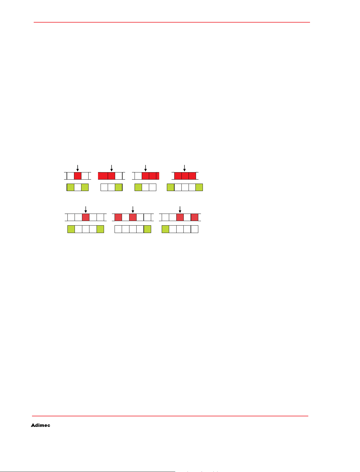
IMAGE AND DATA FORMATTING
NOTE: the offset is defined at the camera output on a 12 bit scale. That means that if the camera is
switched to another output resolutions than 12 bit the actual offset seen on the output will be different.
Assuming the camera is running at a gain value equal to y and a black level equal to x:
Offset on Camera Output with an output resolution of 10 bit = x.y/4
Offset on Camera Output with an output resolution of 8 bit = x.y/16
See par 8.6 for information about output resolution and the the OR command.
For color cameras, the blacklevel command is not available. Use the offset command instead to alter
the output offset.
Defect pixels8.12
Introduction8.12.1.
The OPAL series camera do have a feature to correct for defect pixels real time.
This is done by interpolating the adjacent pixels according to the method illustrated in figures 8.6 and
8.7.
D
D
D
OPERATING AND USER MANUAL OPAL FAMILY
D 0 D
D
D
D
0 ½ ½
Defect pixel correction method on monochrome cameras.Figure 8.6:
0 1
0
0 1
0
½ ½
0
0
x x
D
0 ½ ½ 0 0
Defect pixel correction method on color cameras.Figure 8.7:
D
0
x x
D
0 1 0 0
x x
D
0 1 0 0
D
0
Up to 3 adjacent pixels can be corrected by the above method. More than 3 adjacent defect pixels can
be user programmed, but may not result in a reliable correction.
Adimec does not release cameras with more than 3 adjacent defect pixels upon delivery.
Defect Pixel information8.12.2.
At manufacturing, a table is generated for each individual camera in order to correct for defect pixels.
This table is stored in non volatile memory and can be read back from the camera. The number of
defect pixels and the locations of each defect pixel can be obtained.
Command syntax: DP?n
Where the reply depends on the value of n.
If n = 0:
Reply message: x
57
Page 58

OPERATING AND USER MANUAL OPAL FAMILY
where x = number of defect pixels.
If n> 0
Reply message: x;y
Where x, y are the coordinates of defect pixel number n.
IMAGE AND DATA FORMATTING
NOTE: The left top pixel is referred to as 1;1
To add a defect pixel to the table, the DP command can be used
Command syntax: DPx;y
Where x, y are the coordinates of defect pixel number.
The DP0 (# of defect pixels) register will be updated accordingly.
NOTE: The left top pixel is referred to as 1;1
Adding a Defect Pixel to the table
Removing a Defect Pixel to the table8.12.3.
To remove a defect pixel to the table, the DPR command can be used
Command syntax: DPRx;y
Where x, y are the coordinates of defect pixel number.
The DP?0 register will be updated accordingly.
NOTE: The left top pixel is referred to as 1;1
Defect Pixel Correction state8.12.4.
The camera corrects for defect pixels according to a defect pixel map, programmed at the factory.
This correction can be enabled or disabled.
58
Command syntax: DPEx
Where x = 0 means disabled, 1 means enabled
The actual defect pixel correction setting can be read back from the camera.
Command syntax: DPE?
Reply message: x
Where x = 0 means disabled, 1 means enabled
Defect Pixel test mode.8.12.5.
For diagnostics purposes it is possible to visualize the defect pixel map on the video output by means
of the Defect Pixels Test command.
Command syntax: DPTx
Where x = 0, 1, 2 or 3.
Page 59

IMAGE AND DATA FORMATTING
X TEST MODE
0 disabled, normal image.
1 marks defect pixels white on video
2 marks defect pixels black on video
3 shows defect pixels as white on a black background
Defect pixel test mode.Table 8.6:
The actual setting can be read back from the camera.
Command syntax: DPT?
Reply message: x
Where x = 0, 1, 2 or 3 corresponding to the table 8.6.
Output LookUp Table.8.13
Introduction8.13.1.
The camera has an Output LookUp Table. This table can be used to correct each pixel by a user
specified value. It can be useful if, for instance, Gamma correction is desired.
OPERATING AND USER MANUAL OPAL FAMILY
In order to load the look-up table values, the camera should be prepared to receive the values.
This is done through the OLUTBGN command.
Command syntax: OLUTBGN
NOTE: When an OLUTBGN command is received if the LUT is already opened and/or the LUT is
already (partly) filled, error 120 is issued and the LUT-status is reset.
Output LookUp Table content8.13.2.
The user look up table is loaded by command OLUT. Entries can be retrieved by OLUT?
Command syntax: OLUTx
Where 0 ≤ x ≤ 4095
To fill the OLUT, it should first be opened through the OLUTBGN command.
The Output LookUp Table is based on the 12 bit output resolution. Therefore a total of 4096 values
have to be entered, beginning with the entry replacing the input value 0 up to the input value 4095.
The LUT pointer is incremented at each LUT entry.
NOTE 1: If there is no preceeding OLUTBGN command there will be no action and error result is set to
121.
NOTE 2: If the number of OLUT commands exceeds the LUT size (4096) there will be no action and
error result is set to 123.
Down scaling the output resolution to 8 or 10 bit is done after the LUT.
59
Page 60

OPERATING AND USER MANUAL OPAL FAMILY
Output LookUp Table end.8.13.3.
After filling the output look-up table with 4096 vales, the table should be closed. This is done through
the OLUTEND command.
Command syntax: OLUTEND
NOTE: If the camera did not receive exactly 4096 entries, the LUT definition is ended, but LUT data is
not saved to non-volatile memory. The previous LUT is restored (if no valid LUT was found, a unity LUT
function is used instead) and error result is set to 122.
Output LookUp Table enable.8.13.4.
The user look-up table can be enabled or disabled by means of the OLUTE command.
Command syntax: OLUTEx
Where x is set to 1 for enabling the LUT and 0 to disable the LUT.
The actual setting can be read back from the camera.
IMAGE AND DATA FORMATTING
60
Page 61

SERVICE & MAINTENANCE
Service & Maintenance9.
Diagnostics9.1
Error diagnosis by serial communication protocol9.1.1.
Within the communication protocol, the command and data are combined in a message.
After receiving a message the camera responds with an acknowledgement character. This can be an
ACK character (positive acknowledgement) or a NAK character (negative acknowledgement).
The ACK response is given when the received message was understood (the content of the message
is not considered).
The NAK response is given when the received message was not understood, which may be the case
when invalid characters are received as message content, or the message overruns the camera
receiver buffer capacity.
However, the communication protocol itself does not check the content and validity of a message.
After each attempt to execute a command, the error register is set. To verify whether a command is
succesfully executed or not, the result should be read back from the camera.
Command syntax: ERR?
The ERR command returns a single integer value.
OPERATING AND USER MANUAL OPAL FAMILY
A list of possible error codes and the cause are shown below:
Error code Description
0 No error
1 Last received command: unknown command keyword
2 Last received command: missing parameter
3 Last received command: parameter syntax error
4 Last received command: too many parameters
5 Last received command: missing parameter(s)
7 Last received command: parameter(s) out of range
8 Last received command: internal Adimec error
100 Loading of settings configuration from non-volatile memory failed (CRC invalid)
101 Writing of settings configuration to non-volatile memory failed (CRC verify failed)
102 DP: adding a defect while the list is already full
103 DP: adding a defect that is already in the list
120 OLUTBGN operation error: LUT transactions already pending.
121 Adding OLUT element or OLUTEND while OLUT definition not opened by OLUTBGN.
122 OLUTEND while received not enough LUT entries.
123 Adding more LUT entries that allowed.
Possible error codesTable 9.1:
61
Page 62

OPERATING AND USER MANUAL OPAL FAMILY
Built-In Test9.1.2.
After power up a number of built-in tests are performed to check on correct camera operation. The
result of these tests can be obtained by the BIT command.
Command syntax: BIT?
Reply message : x;y
Where x;y = 0;0 indicates all tests passed.
NOTE: All other codes are of no meaning to the user. When requesting support on some features of
the camera, Adimec may request the result of the BIT command, in order to optimize support.
Camera temperature9.1.3.
The temperature of the sensor pcb inside the camera can be obtained by means of the Temperature
Measurement command..
Command syntax: TM?
Reply message : x;y
Where x = temperature in °Celsius and y = temperature in °Fahrenheit
SERVICE & MAINTENANCE
Elapsed time9.1.4.
The amount of time the camera has been powered on after manufacturing can be obtained from the
camera by means of the elapsed time command.
Command syntax: ET?
Reply message : x;y
Where the total elapsed time in hours is defined as x * 65536 + y.
Microcontroller firmware release time stamp9.1.5.
For diagnostic purposes on firmware issues the time stamp (date and time) of the internal
microcontroller firmware can be obtained from the camera.
Command syntax: UFDT?
Reply message : “Mon dd YYYY;hh:mm:ss
Where Mon dd YYYY represent the date and hh:mm:ss the time.
NOTE: This command gives no practical user information. When requesting support on some features
of the camera, Adimec may request the microcontroller timestamp, in order to optimize support.
62
Page 63

SERVICE & MAINTENANCE
Internal test pattern generator9.2
In order to check the camera and datapath in the system, a test pattern is available. This test pattern
generator produces a static, defined picture according to the settings for output resolution, gain and
the mode the camera is currently working in. Binning and mirror settings are not functional. The output
values of the test pattern are subject to the applied gain. The test pattern is developed with gain = 1
and therefore hereafter described as if gain were set to 1.
The following command switches the test pattern on or off.
Command syntax: TPx
Where x = 0 for off, 1 for on
The current setting can also be read back from the camera.
Command syntax: TP?
Test pattern definition9.2.1.
The test pattern image is specified in 12 bit digital values. When an output resolution m < 12 bit is
selected the camera will output the upper m bits of the specified values discarding non-used
lower bits.
OPERATING AND USER MANUAL OPAL FAMILY
For 8 and 10 bit output the values truncates as follows:
RELATIVE VALUE 12 BIT DOMAIN 10 BIT DOMAIN 8 BIT DOMAIN
Black 0 % 0 0 0
100
200
300
15 3 0
(G)ray / 50 %
.
(W)hite / 100 % 4095 1023 255
Test pattern mapping 8 to 12 bit domain.Table 9.2:
2047
..
511
..
127
..
Global layout9.2.2.
The test pattern has a size equal to the maximum active video area size. The size is defined by the
parameters W and H according to the table below:
CAMERA TYPE W H
OPAL-1000 1024 1024
OPAL-1600 1600 1200
OPAL-2000 1920 1080
OPAL-4000 2336 1752
OPAL-8000 3296 2472
Test pattern size.Table 9.3:
63
Page 64
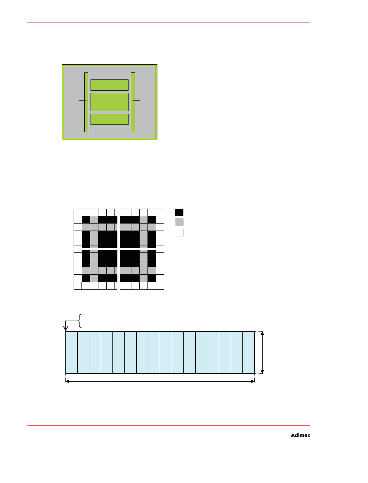
OPERATING AND USER MANUAL OPAL FAMILY
The test pattern is composed of a black (digital 0) background with superimposed sub-patterns
according to the layout shown below:
Border
Pattern
Top gray bars
SERVICE & MAINTENANCE
Color
Bar
Gray patches
Bottom gray bars
Test pattern layout.Figure 9.1:
Color
Bar
The Color bar patterns only apply to color cameras. Monochrome cameras have these areas blanked.
Border pattern9.2.3.
1 2
1
2
3
4
H-4
H-3
H-2
H-1
)
3
4
W-4
W-3
W-2
W-1
W
2047
4095
0
64
Top gray bars9.2.4.
x = W/2 - 255
y = H/2 - 334
255
511
Horizontal center
767
1023
1279
1535
1791
2047
2303
2559
2815
3071
3327
3583
3839
166
4095
512
Page 65
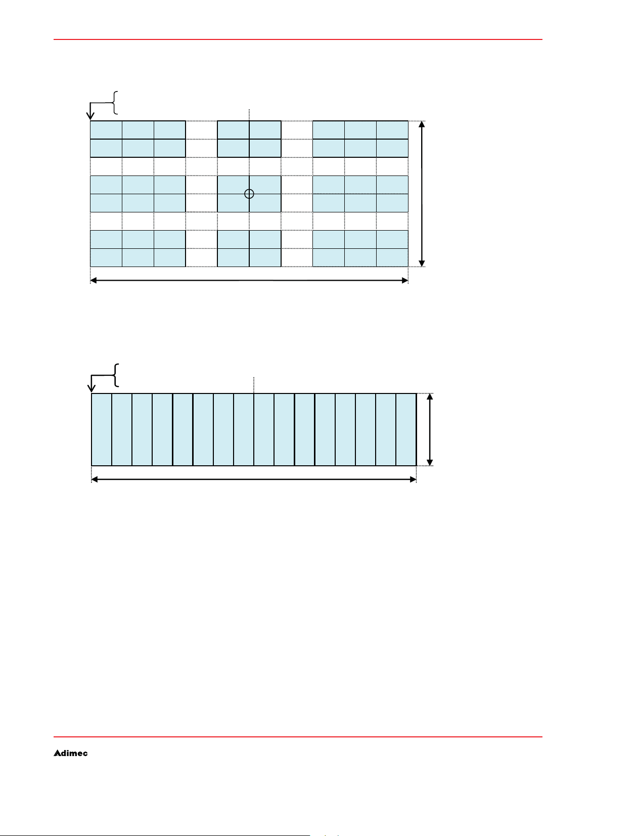
SERVICE & MAINTENANCE
Gray patches9.2.5.
x = W/2 - 255
y = H/2 - 127
OPERATING AND USER MANUAL OPAL FAMILY
1
128 0 129
Size of each patch: 4H x 8V
2
130
Bottom gray bars9.2.6.
x = W/2 - 255
y = H/2 + 170
63
191
1983
2111
3903
4031
64
192
1984
2112
3904
4032
512
Horizontal centre
125
253
126
254
127
255
2047 2046 2045 1922 1921 1920
256
2175 2174 2173 2050 2049 2048
3967 3966 3965 3842 3841 3840
4095 4094 4093 3970 3969 3968
166
255
511
767
1023
1279
1535
1791
2047
2303
2559
2815
3071
3327
3583
3839
4095
512
65
Page 66
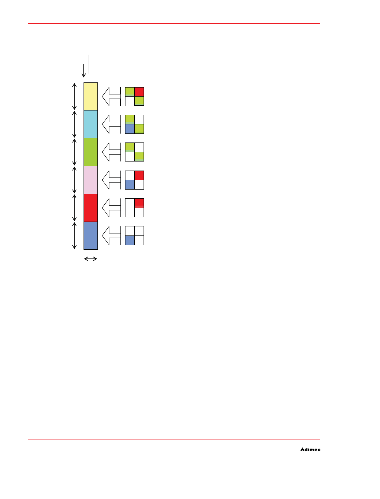
OPERATING AND USER MANUAL OPAL FAMILY
9.2.7. Color bar
Left: x = w/2 - 319
Right: x = w/2 + 289
Y - pos: y = h/2 - 437
G
146
146
146
146
X
G
B
G
X
X
B
R
G
X
G
X
G
R
X
SERVICE & MAINTENANCE
R
X
146
146
32
NOTE: The colored pixels indicated “On” have a value of 4095. Pixels indicated “X” have a value of 0.
X
X
X X
B
X
Information Overlay data format9.3
When enabled, the top left most active video pixels in the output image are replaced by 8 data pixels.
The upper 8 bits of the data pixels carry information, lower bits (when applicable) are set 0.
Command syntax: OVLx
Where x = 0 disables the overlay function and x = 1 enables the overlay function.
The overlay data contains two 32 bit values:
The current frame counter •
The actual integration time used for the current image. The integration time value is supplied in •
units of 1 pixel clock interval (25 ns).
66
The actual setting can be read back from the camera.
Page 67
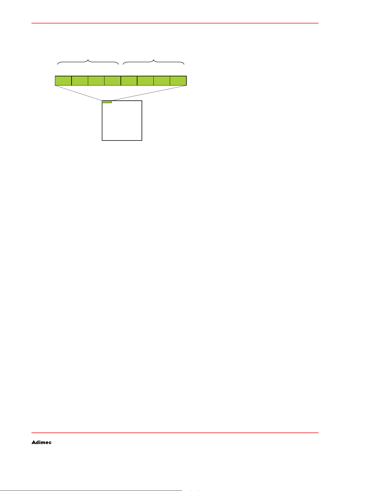
SERVICE & MAINTENANCE
7:0
Pix(7)
Current frame counter
Integration time
The data pixel layout is shown below:
Pix(1) Pix(2) Pix(3) Pix(4) Pix(5) Pix(6)
Pix(0)
32:24 23:16 15:8 7:0 32:24 23:16 15:8
Graphic representation of overlay data layout.Figure 9.2:
Cleaning9.4
Cleaning of the camera.9.4.1.
The camera must never be immersed in water or any other fluid. For cleaning, only use a light moist
cotton tissue.
OPERATING AND USER MANUAL OPAL FAMILY
Output
Image
Cleaning of the CCD sensor9.4.2.
Cleaning of a CCD sensor is a rather difficult task. Due to the possibility of creating scratches on the
cover glass or damaging the CCD by ESD, Adimec does not recommend cleaning the optical surface
of the sensor, unless by necessity.
Depending on the aperture of the lens used, any dust particles with a size of 7 μm and larger can •
show up in your image.
All cameras are checked to be clean in the factory before shipment. •
Proper handling instructions during system assembly and integration can prevent the CCD sensor •
from becoming contaminated.
Should cleaning of the CCD sensor be unavoidably necessary, follow the lprecaution below.•
The correct work environment for cleaning is essential in order to ease cleaning and to prevent
damage of the CCD sensor.
67
Page 68

OPERATING AND USER MANUAL OPAL FAMILY
Precautions:
Take general precautions to prevent ESD that can damage the CCD sensor•
Cleaning of the CCD sensor, and assembly of the lens is preferably performed in a clean room or •
at least at a clean bench.
Never try to clean the CCD sensor at a relative humidity lower than 30 %. A relative humidity of •
40 % or higher is preferred in order to minimize the chance of damage due to ESD.
It is advisable to use an ionizer, in order to minimize the built-up of electrostatic charges.•
Use non-fluffing cotton swab and Alcohol (or Hexane) for cleaning. De-ionized water may be •
necessary to remove ionic contaminants like salts.
A cotton swab should be used only once - you will otherwise move dirt from one place to another.•
Never rub the window dry. This may cause static charges or scratches that can destroy the CCD •
sensor.
Cleaning directions:
First try to remove the contamination by using clean, dry air. Use an ultra-filtered, 1.
non-residue dust remover spraycan. Dry air can cause an electrostatic charge. Take
appropriate environmental measurements to avoid the build-up of electrostatic
charges. Prevent blowing air in the thread of the lensmount, because this may cause
contamination on the CCD sensor due to loose particles and traces of oil or grease.
If this step does not result in an acceptable result, continue with step 3.2.
Remove the lens mount by removing the 4 crosshead screws that hold the lensmount. Clean 3.
the inner side thread of the lens mount using Alcohol or Hexane and a cotton swab.
Clean the CCD cover glass using Alcohol or Hexane and a cotton swab. Gently and 4.
carefully rub the window always in the same direction, e.g. top to bottom.
Install the lensmount back onto the camera.5.
Check the results of the cleaning operation.
Install a lens and power up the camera. Adjust the lens at a small aperture (f.i. F16) and 6.
point the lens at a bright lightsource. Adjust gain and integration time if necessary.
Check the image on the monitor for dark spots and stripes caused by contamination 7.
on the CCD sensor cover glass. (Note that the image on the monitor should not
saturate due to over exposure - if necessary close the iris even further).
If the CCD sensor is not clean, repeat steps 3 - 7 using a new cotton swab. After three 8.
unsuccessful tries, it is advised to wait a few minutes before a new attempt is made to clean the
CCD sensor. (This allows the electric charge that has been built up during cleaning to neutralize).
If the cleaning operation is not successful, it is recommended that you contact your business office
service department to get the appropriate support.
SERVICE & MAINTENANCE
68
Maintenance9.5
No specific maintenance other than cleaning is applicable.
Repair and modification9.6
Repair, modification and replacement of parts shall be done only by Adimec to maintain compliance
with the directive 89/336/EEC electromagnetic compatibility
Page 69
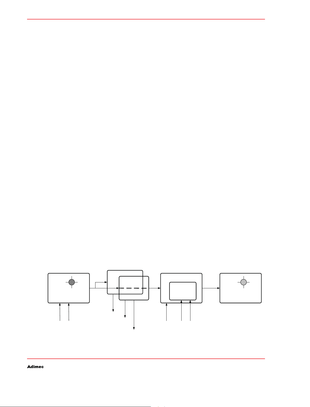
OPTION: AEC/VEM
Option: AEC/VEM10.
Introduction10.1
The AEC option is available on all OPAL family members. This application note describes the
functionality of the option.
AEC stands for Automatic Exposure Control. In the OPAL camera series this breaks down into two
basic functionalities:
• Automatic Gain Control
• Automatic Integration time Control
The VEM option is available on the monochrome OPAL family members only.
VEM stands for Video Enhancement Module. This function optimizes contrast for the whole image
based on real-time measurements made on a predefined window within the image.
The camera can be operated as any standard OPAL camera for setting the parameters described in
this Application Note.
In this Application Note the following abbreviations will be used:
OPERATING AND USER MANUAL OPAL FAMILY
AGC: Automatic Gain Control
AIC: Automatic Integration time Control
AEC: Automatic Exposure Control: the combination of both AIC and AGC
Performance10.2
AEC10.2.1.
The Automatic Exposure Control is fully configurable. The measurement window can be set; the auto
exposure setpoint is adjustable. These parameters are common for both Automatic Gain Control and
Automatic Integration time Control.
Both AIC and AGC can be enabled separately. The AIC will control in discrete steps. Therefore it is
advised to always have both AGC and AIC enabled; in this configuration the AGC will act as a finetuning mechanism for the AIC. If the AIC is enabled and AGC is disabled, gain will be set to last gain
set by the automatic gain control or manual gain.
IMAGE-DATA
CCD
MEASUREMENT
AECWIN
VEMWIN
GAIN / BLACKLEVEL
AGC
COMPLETE IMAGE
VEM
EQUAL TO
MEASUREMENT
WINDOW OR
COMPLETE IMAGE
DIGITAL IMAGE OUT
=> SETPOINT !
AEC_MEAN
TON
TOFF
AIC
This figure indicates the control loop of AEC.Figure 10.1:
VEM_MEAN
VEM_PEAK_MINIMUM
AEC_GA
VEM_GA
VEM_BLACK
69
Page 70
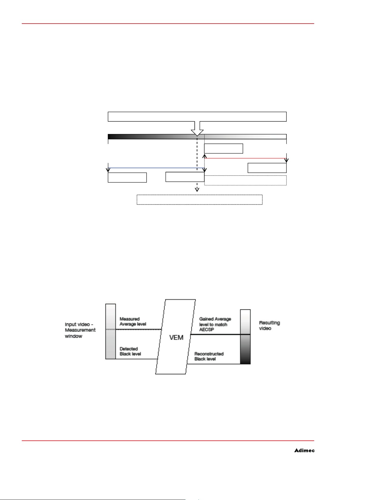
OPERATING AND USER MANUAL OPAL FAMILY
The detection value of the AEC mechanisms is the weighted average within a defined window of the
grey value (monochrome cameras, default the weighing factor is 1) or the weighted average of the red,
green and blue information (red + green + blue = 1).
AIC acts at sensor level. Ton and Toff in figure 1 are internal timing signals which determine the
integration period of the sensor. This timing is the result of the algorithm using the Frame Period (FP),
the measured average video level from sensor (AEC_mean) and the Auto Exposure Setpoint.
AGC will act if the Auto Exposure Setpoint cannot be matched by the AIC due to low light conditions.
In this case, the integration time is at maximum with regards to AICmax and FP.
Scene light level
AIC control
OPTION: AEC/VEM
Auto Exposure SetPoint
Maximum IT
AGC control
This figure indicates the operation of the AEC control loopFigure 10.2:
Maximum GA
Minimum GA
AEC status: IT = maximum, GA >minimum
GA acts as fine adjust
Minimum IT
The speed factor of both AIC and AGC controls can be set by user command.
VEM10.2.2.
This function optimizes contrast for the whole image based on real-time measurements made on
a predefined part of the image, referred to as detector window or Area Of Interest (AOI). Contrast
optimization is done by applying gain and offset in order to have pre-defined maximum and minimum
video levels in the AOI. The part of the image that is outside the AOI will also be optimized but will not
contribute to the real time measurements. These parts may therefore remain over- or underexposed.
70
This figure indicates the operation of the VEM control loopFigure 10.3:
VEM allows for contrast enhancement by video level measurements within a defined window. The
operation and its limits can be configured by commands.
Page 71

OPTION: AEC/VEM
The default values for VEM operation are selected as best trade-off between applied enhancement and
noise. It is best to keep this default setting.
If noise becomes an issue, than parameter VEM maximum AGC gain might be decreased in order to
have less overall gain.
AEC commands10.3
All parameters in which the camera differs from the standard camera will be discussed in this chapter.
For all parameters goes: where applicable the default setting is underlined.
Auto exposure control commands10.3.1.
All commands with a question mark are query commands, obtaining information from the camera. All
other commands are commands with which a certain parameter is set. For all parameters goes: where
applicable the default setting is underlined.
Enabling AEC (AIC & AGC)10.3.2.
Automatic gain control (AGC) and automatic integration time control (AIC) can be enabled
independently.
Command syntax: AGCx
Where x=0: AGC disabled
OPERATING AND USER MANUAL OPAL FAMILY
x=1: AGC enabled
Command syntax: AGC?
Reply: x
Where x: as above
Command syntax: AICx
Where x=0: AIC disabled
x=1: AIC enabled
Command syntax: AIC?
Reply: x
Where x: as above
71
Page 72

OPERATING AND USER MANUAL OPAL FAMILY
Controlling AEC setpoint and measurement window10.3.3.
Setpoint and window are common for AGC and AIC and can be altered with the AECSP (setpoint) and
AECWIN (window) commands respectively.
Command syntax: AECSPx
Where x= 0 .. 4095
NOTE: x= 0 : setpoint at absolute black
x= 1024: setpoint at 1/4 x Full Scale
x= 4095: setpoint at Full Scale
Command syntax: AECSP?
Reply: x
Where x: as above
Command syntax: AECWINx;y;w;h
Where x = 0 .. left side of window/HBIN factor
OPTION: AEC/VEM
y = 0 .. top of window/VBIN factor
w= 2 .. width of window/HBIN factor
h= 2 .. height of window/VBIN factor
Command syntax: AECWIN?
Reply: x;y;w;h
Where x, y, w and h as above
NOTE:
1) Values are automatically adjusted if needed to correct values. All values are rounded to even values.
2) After an ROI command, the AEC window will automatically be changed to the ROI-values.
3) The AEC setpoint is also the setpoint for VEM.
Controlling AEC Peak / Average balance10.3.4.
the balance between peak and average can be set by the AECPAB command.
Command syntax: AECPABx
Where x= 0 .. 256
NOTE: x= 0 : completely average
72
x= 256 : completely peak
Page 73

OPTION: AEC/VEM
Command syntax: AEPAB?
Reply: x
Where x: as above
Weight of the R, G and B values for AEC (color only)10.3.5.
To determine the luminance value that is to be compared to the setpoint value each primary color
has its own weight. In general this is considered necessary because the human eye has different
sensitivities for the three primary colors. The optimum settings however do very much depend on the
scene illumination and the application in which the camera is used.
Therefore the default settings are equal for each of the colors.
Command syntax: AECLUMr;g;b
Where r = 0 .. 100 = relative weight of red info in units of 0.01
g = 0 .. 100 = relative weight of green info in units of 0.01
b = 0 .. 100 = relative weight of blue info in units of 0.01
NOTE: r + g + b = 100, Values added together must not exceed 100 (1 time gain) in total, otherwise
parameter range error.
OPERATING AND USER MANUAL OPAL FAMILY
Command syntax: AECLUM?
Reply: r;g;b
Where r, g and b as above
73
Page 74

OPERATING AND USER MANUAL OPAL FAMILY
Defining AEC behavior10.3.6.
Four advanced parameters, defining AEC behavior can be set and read back by means of the AECP
command. Refer to table below for a description of these parameters and their default values.
Command syntax: AECPx;y
Where x = AEC parameter
y = parameter value
Command syntax: AECP?x
Reply: y
Where x and y as above
x range of the setting parameter value description
0 1 .. 255 AGC Speed factor. High factor is fast response
1 100 .. 12799 AGC maximum gain in units of 0.01 times
2 1 .. 32000 AIC minimum time in units of 10 us
3 1 .. 32000 AIC maximum time in units of 10 us
6* - Current mean detection value
7* - Current peak detection value
8* - Current peak / mean ratio value
9 0 .. 9 Softness factor peak detector
* read only
OPTION: AEC/VEM
Range of the AEC settings Table 10.1:
VEM commands (Monochrome only)10.4
All commands with a question mark are query commands, obtaining information from the camera. All
other commands are commands with which a certain parameter is set. For all parameters goes: where
applicable the default setting is underlined.
Enabling the VEM10.4.1.
Although VEM can be enabled independent from AGC and AIC, it is recommended that at least AIC is
enabled. This allows the camera to auto select the integration time necessary for nominal video.
Command syntax: VEMx
Where x=0: VEM disabled
x=1: VEM enabled
Command syntax: VEM?
Reply: x
Where x: as above
74
Page 75

OPTION: AEC/VEM
Controlling the AEC setpoint and VEM measurement window10.5
Setpoint and window can be altered with the AECSP (setpoint) and ARCWIN (window) commands
respectively
Command syntax: AECSPx
Where x= 0 .. 4095
NOTE: x= 0 : setpoint at absolute black
x= 1024: setpoint at 1/4 x Full Scale
x= 4095: setpoint at Full Scale
Command syntax: AECSP?
Reply: x
Where x: as above
Command syntax: VEMWINx;y;w;h
Where x = 0 .. left side of window/HBIN factor
OPERATING AND USER MANUAL OPAL FAMILY
y = 0 .. top of window/VBIN factor
w= 2 .. width of window/HBIN factor
h= 2 .. height of window/VBIN factor
Command syntax: VEMWIN?
Reply: x;y;w;h
Where x, y, w and h as above
75
Page 76

OPERATING AND USER MANUAL OPAL FAMILY
Defining VEM behavior10.5.1.
Six advanced parameters, defining VEM behavior can be set and read back by means of the VEMP
command. Refer to table below for a description of these parameters and their default values.
Command syntax: VEMPx;y
Where x = advanced parameter
y = advanced parameter value
Command syntax: VEMP?x
Reply: y
Where x and y as above
x range of the setting parameter value description
0 1 .. 255 Control Speed factor. High factor is fast response
1 0, 1 0 VEM active on complete window (ROI)
2 1 .. 12799 VEM maximum AGC gain in units of 0.01
3 1 .. 12799 VEM maximum contrast gain budget in units of 0.01
4 1 .. 12799 VEM maximum contrast Gain in units of 0.01
5 0 .. 9 VEM softness factor minimum detection
6* 0 ..4095 The current mean detection value used by the VEM in
7* 0 ..4095 The current minimum detection value used by the VEM
8* 0 ..4095 The current gain value used by the VEM
9* -4095 .. 0 The current black level value used by the VEM
OPTION: AEC/VEM
1 VEM active on VEM window only
12 bit video resolution
in 12 bit video resolution.
*read only
Range of the VEM settingsTable 10.2:
76
Page 77
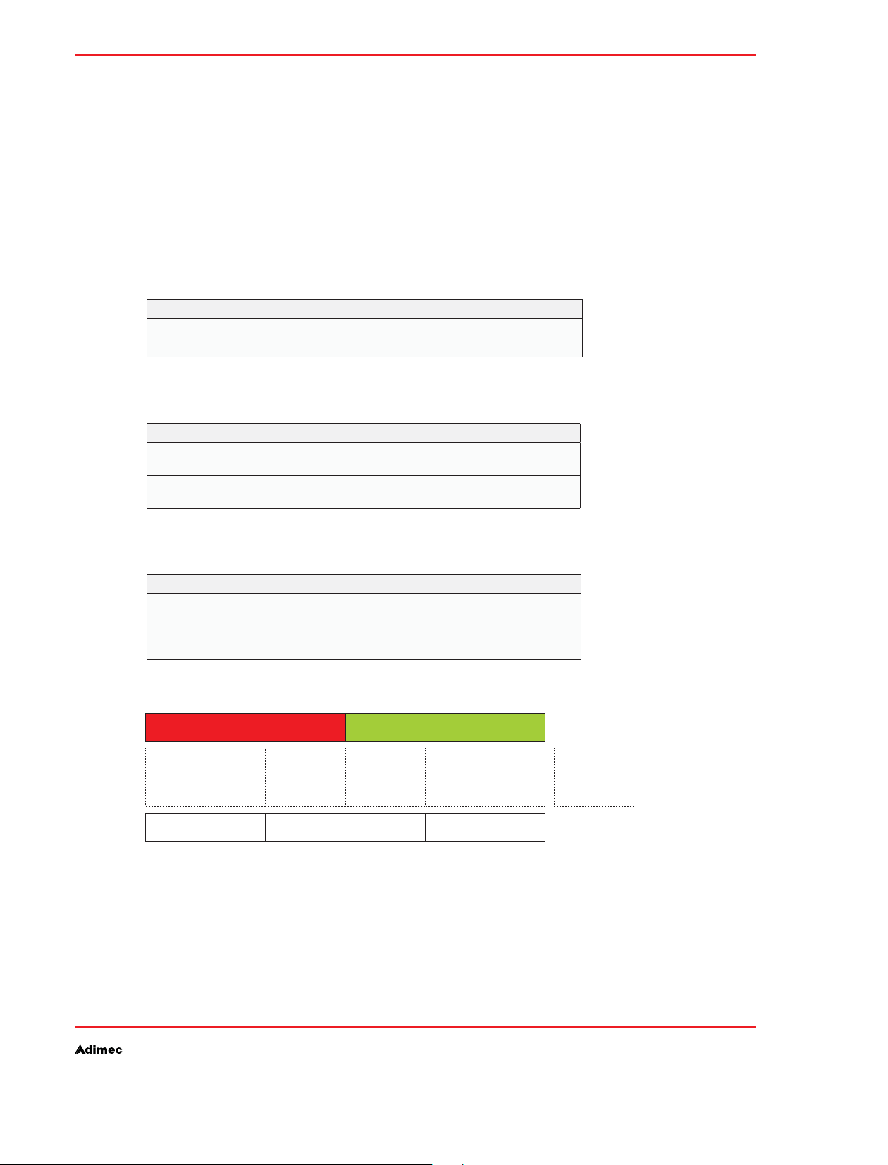
REFERENCE
Reference11.
Camera Link port configuration11.1
The two video outputs TAP-A and TAP-B of the camera are mapped to the Camera Link ports A, B and
C according to the base configuration described in the Camera Link specification.
The mapping for 8,10 and 12 bit output resolution is shown in the tables below. All unused Port A/B/C
signals are set to logic 0.
The DVAL signal is fixed to logic 1.
The mapping for 8 bit output resolution is shown below:
CAMERA OUTPUT PHYSICAL CAMERA LINK PORT MAPPING
TAP-A (bit 7..0 ) Port A (7..0)
TAP-B (bit 7..0) Port B (7..0)
The mapping for 10 bit output resolution is shown below:
CAMERA OUTPUT PHYSICAL CAMERA LINK PORT MAPPING
TAP-A (bit 9..8 )
TAP-A (bit 7..0 )
TAP-B (bit 9..8 )
TAP-B (bit 7..0 )
OPERATING AND USER MANUAL OPAL-FAMILY
Mapping for 8 bit output resolutionTable 11.1:
Port B (1..0)
Port A (7..0)
Port B (5..4)
Port C (7..0)
Mapping for 10 bit output resolutionTable 11.2:
The mapping for 12 bit output resolution is shown below:
CAMERA OUTPUT PHYSICAL CAMERA LINK PORT MAPPING
TAP-A (bit 11..8)
TAP-A (bit 7..0)
TAP-B (bit 11..8)
TAP-B (bit 7..0)
Mapping for 12 bit output resolutionTable 11.3:
Port B (3..0)
Port A (7..0)
Port B (7..4)
Port C (7..0)
TAP-A TAP-B
0 . . . . . . 7
0 . . . . . . 7
8 . .11
0 . . 3
8 . .11
4 . . 7
0 . . . . . . 7
0 . . . . . . 7
Port-A Port-C Port-B
Figurative representation of two tap Camera Link 12-bits bit mapping in 12-bits.Figure 11.1:
<= Bit
assigment to
<= Pin
77
Page 78
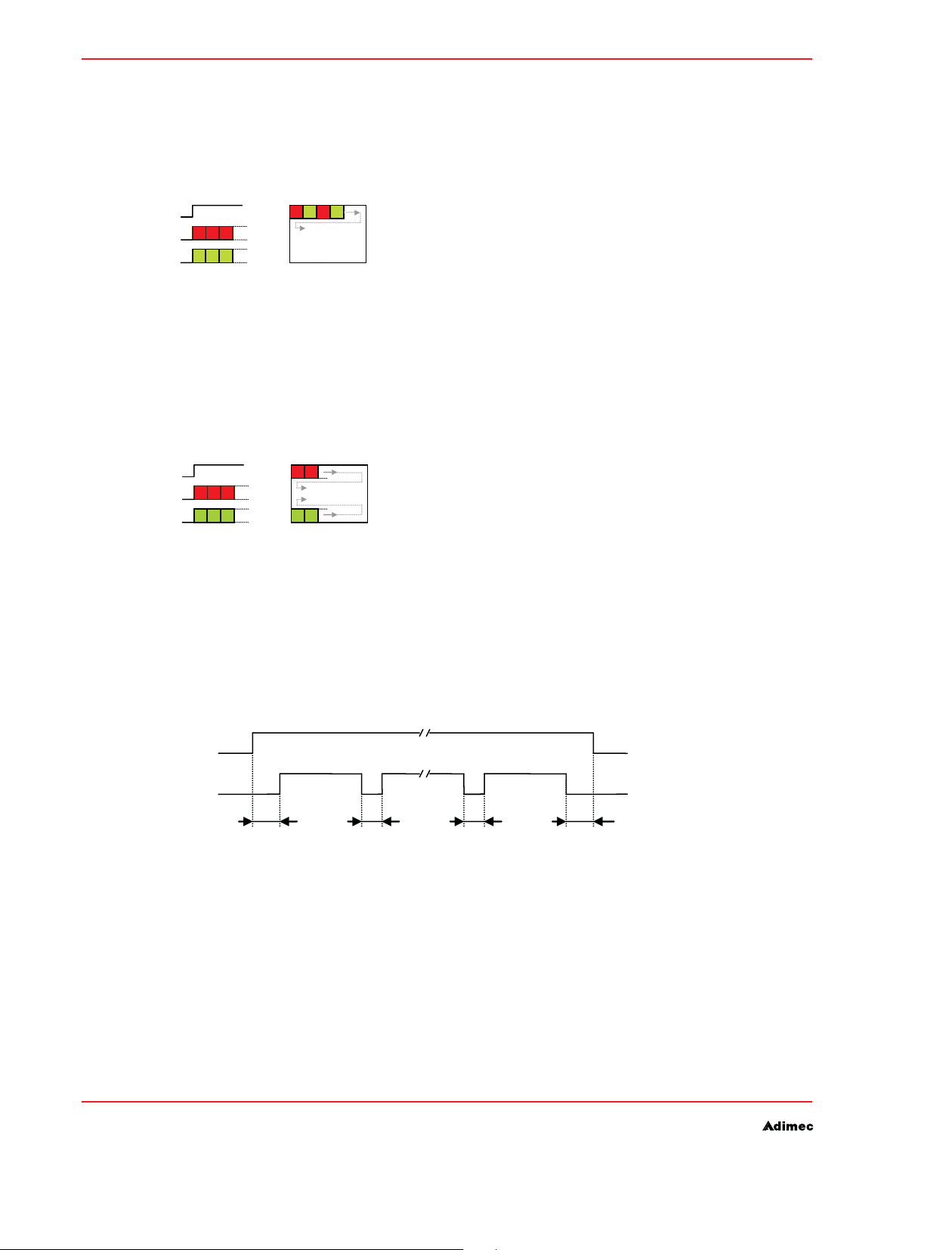
OPERATING AND USER MANUAL OPAL-FAMILY
T
Lef
Righ
T
Lef
Righ
Camera Link video output11.2
Vertical Remap enabled:11.2.1.
If vertical remap is enabled the camera has the tap stream format as shown in fig. 10.2.
op
1
1
2
t
Output image
2
1
t
Output image
2
1
2
Bottom
op
Bottom
t
t
LVA L
23
1
Tap A
2 3
1
Tap B
Camera Link video timing Vertical remap enabled.Figure 11.2:
The latency with vertical remap enabled is about 52% of the minimum frame period.
Vertical Remap disabled:11.2.2.
If vertical remap is disabled the camera has a tap stream format as shown in fig. 10.3.
LVA L
23
1
Tap A
2 3
1
Tap B
REFERENCE
Camera Link video timing Vertical remap disabled.Figure 11.3:
The latency with vertical remap disabled is about 2% of the minimum frame period.
NOTE: Latency is defined as the time between the end of the camera integration period and the start
of image output on the camera output.
Camera Link video timing caracteristics11.2.3.
FVAL
LVAL
tg1 tg1 tg2 tg2
Camera Link video timingFigure 11.4:
Time between FVAL rising edge and first LVAL rising edge tg1 • ≥ 16 Tp.
LVAL inactive period tg2 • ≥ 4 Tp
Time between last LVAL falling edge and FVAL falling edge tg1 • ≥ 16 Tp ,
where Tp = interface clock period
Note that the LVAL signal is not a continuous signal and that the time between successive LVAL
periods (tg2 in the timing diagram) is not fixed but depends on the image format and possibly inserted
shutter operation. For details on shutter operations during image readout please refer to chapter 7.
78
Page 79
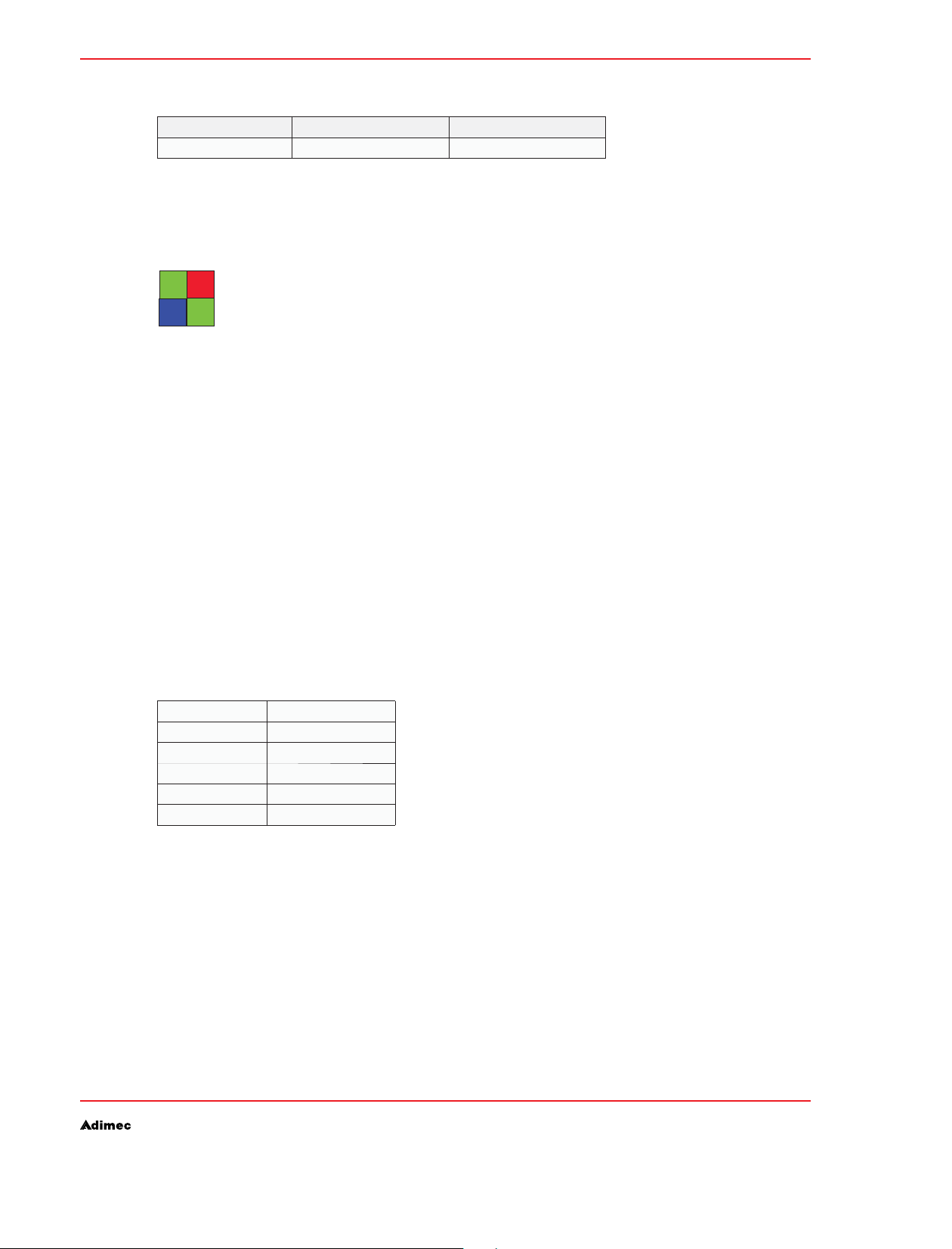
REFERENCE
Pixelclock11.2.4.
MODEL PIXELCLOCK CLOCK PERIOD (TP)
For all OPAL models 80 MHz 1.25 ns
Bayer pattern color cameras11.2.5.
The OPAL cameras use the following Bayer pattern for color encoding:
___
The first pixel on the first line is basically the first pixel of a frame that is output by the camera is the
pixel on left-top in fig. 10.4. This pixel is a so-called “Green Pixel On a Red Line.”
When using the horizontal and/or vertical flip functions, the Bayer pattern will also be mirrored.
Basic serial communication parameters of the camera11.3
OPERATING AND USER MANUAL OPAL-FAMILY
Pixelclock speedTable 11.4:
GGR
B
Bayer pattern.Figure 11.5:
Control of the camera by serial communication11.3.1.
The OPAL camera is fully software controlled via the Camera Link cable using a ASCII based protocol.
Delivered with the camera is a command line based console application that can be used to
interactively control the camera. It can also load and save power-up default settings.
Although this is an easy option of changing camera settings it is also possible to communicate with
the camera using your own dedicated software.
Data link settings11.3.2.
The data link settings that shall be used for communication with the camera are:
DESCRIPTION PARAMETER
Baudrate 57600 baud
Stop bit 1
Data bit 8
Parity none
Handshaking none
port settingsTable 11.5:
79
Page 80

OPERATING AND USER MANUAL OPAL-FAMILY
Data flow characters11.3.3.
The communication protocol uses data flow control characters to identify a message and for
acknowledgement.
The following data flow characters are defined:
CHAR DEC DESCRIPTION
NUL 0 NUL character, is ignored
STX 64 start of message identifier
ETX 13 end of message identifier
ACK 6 positive acknowledgement
NAK 21 negative acknowledgement
Used ASCII control charactersTable 11.6:
Message Format11.3.4.
Command and data are combined in a message. A message starts with the STX character followed
by the message content. The message ends with an ETX character. The characters allowed in the
message content range from decimal 32 to 255.
Format: STX <message content> ETX
REFERENCE
Message acknowledgement11.3.5.
After receiving a message, the camera responds with an acknowledgement character. This can be an
ACK character (positive acknowledgement) or a NAK character (negative acknowledgement).
The ACK response is given when the received message was understood (the content of the message
is not considered).
The NAK response is given when the received message was not understood, which may be the case
when invalid characters are received as message content, or the message overruns the camera
receiver buffer capacity.
Reply messages11.3.6.
When a message is sent to the camera that requires data to be transmitted back to the host system
this data is packed in a message and is sent to the host system after the positive acknowledgement
(ACK) character. When the camera responds with a NAK character no data is sent back to the host
system.
Communication timing11.3.7.
The time between the successive characters making up a message is not limited. The camera
however, when transmitting a message to host system, has a time interval between successive
characters of less than the time required for a single character to be transmitted.
80
Page 81
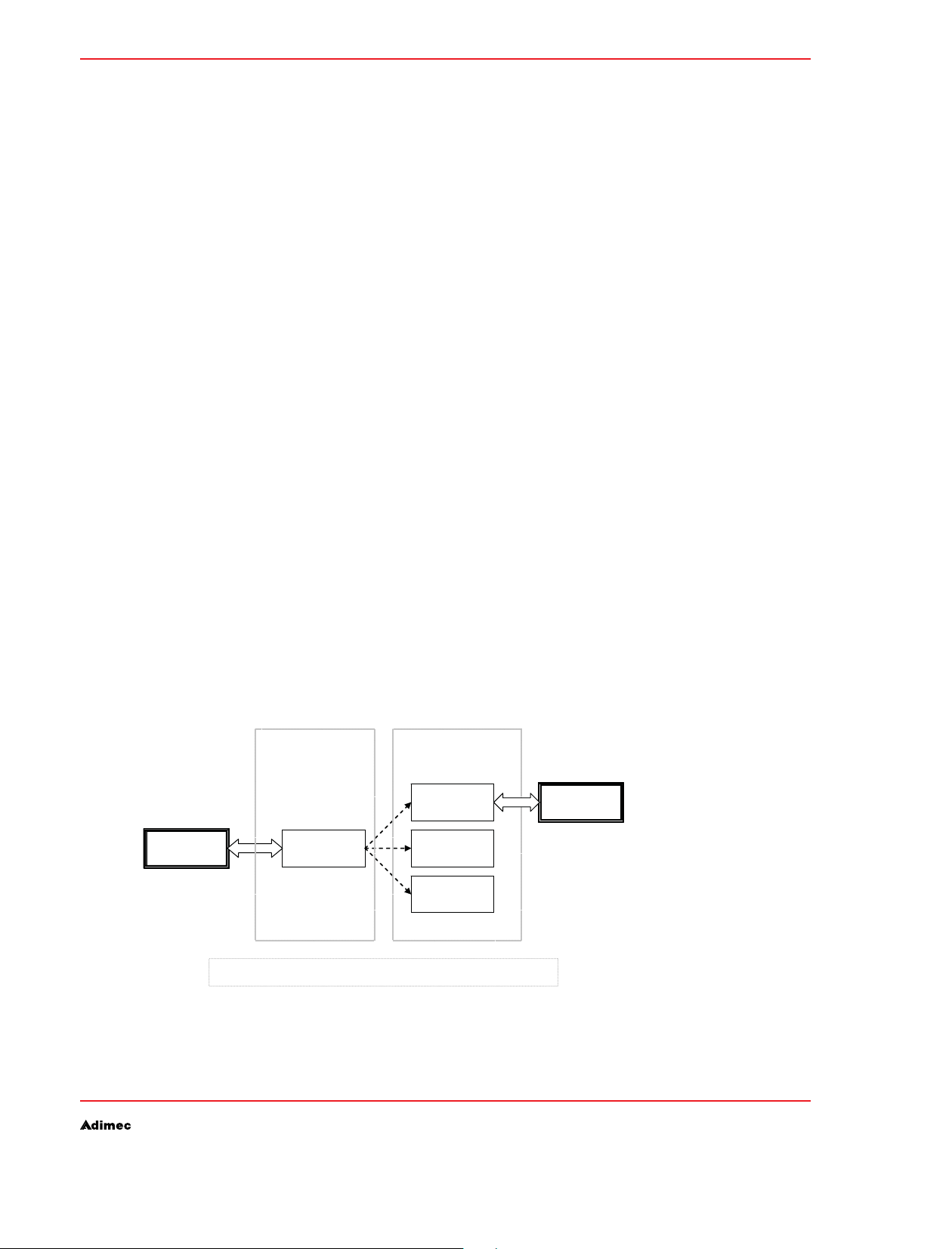
REFERENCE
pp
Host system requirements11.3.8.
Camera Link interface standard11.4
Introduction11.4.1.
Without getting into detail on the Camera Link standard, this section discusses the mechanics of the
serial communication channel.
OPERATING AND USER MANUAL OPAL-FAMILY
After transmitting a message to the camera, the host system must wait for the camera to reply •
with an ACK or NAK character. To prevent lock-up, the wait time for the response must be limited
by a time-out period. If the host systems has not received an ACK or NAK character after the
time-out period has elapsed, the host system must consider the transmitted message as not
being received.
The time-out time to be used for the camera should be at least 200 ms.•
Under normal conditions a NAK or no response from the camera results from damage of the •
transmitted characters due to noise or communication link hardware problems. In such case, the
host system should transmit the message again. The number of repeated transmissions after a
NAK response or no response must be limited by a retry count to prevent lock-up.
After the maximum number of retries of the transmitted message, if the camera is still responding •
with a NAK character, the communications channel should be considered malfunctioning or too
noisy.
After the maximum number of retries of the transmitted message if the camera is still not •
responding, the communication channel should be considered disconnected or the camera not
being powered or malfunctioning.
Available Camera Link serial software enhancements in the form of Dynamic Link Library files will
greatly simplify the setup of a communication channel.
Both camera manufacturers and frame grabber vendors have issued these DLL files which will provide
standard C, API and native Visual Basic support, so that applications written in C or Visual Basic can
communicate serially with Camera Link cameras.
Overview11.4.2.
The user application calls into the generic clserial.dll, which dynamically loads the.dll file(s) specific to
the frame grabber(s) referred to by the application. It then routes all calls to that .dll file. The following
diagram illustrates this sequence:
Supplied by framegrabber
manufacturer
clser
xxx
.dll
clser
yyy
.dll
clser
zzz.
dll
Camera CL
control lines
a
Supplied by camera
manufacturer
User
lication
xxx, yyy, zzz are unique identifiers, assigned to AIA member companies.
clserial.dll
Mechanics of communication per Camera link serial channelFigure 11.6:
81
Page 82

OPERATING AND USER MANUAL OPAL-FAMILY
Features Provided by clserial.dll
Simultaneous, multi-port (including cross vendor) support•
Support for binary or text based data transfers•
Common API across vendors•
Common error codes across vendors•
Common error text across vendors •
Strict, well defined behavior of all functions in specification•
Openness to vendor specific error codes and text•
Ability to enumerate ports on sytem•
Inquireable/adjustable baud rate for ports•
Win 32 support (open source for port to other platforms)•
C/C++ support through import library•
VisualBasic support through type library•
Backwards compatibility with recommended specification of October 2000•
Standard default communication settings for serial port•
Mechanics of clserial.dll11.4.3.
When clserial.dll loads, it searches the operating system’s system directory (for example,
C:\windows\system or c:\winnt\system) for all files that use the naming convention clserxxx.dll
(xxx is uniquely assigned to AIA member companies). Clserial.dll then dynamically loads those .dll
files and queries each one for its manufacturer name and port names. This action produces a list of all
possible ports.
REFERENCE
The application can then select which port or ports it would like to communicate through. The required
manufacturer specific .dll files will be loaded and clserial.dll will manage passing the application calls
to
the appropriate .dll for the application specified port.
Further details can be found in the Camera Link – Specification of Camera Link Interface Standard for
Digital Cameras and Frame Grabbers – Version 1.1 - January 2004.
Camera command set overview11.5
COMMAND DESCRIPTION
BIT? Gets Built-In Test result (like FPGA boot status, LUT status) in 16 bits
BL Sets the black level. (B/W only)
BL? Gets the black level. (B/W only)
BCNT? Gets the number of images present in the burst memory
BMO Sets the mode to receive images from the burst memory
BMO? Gets the mode to receive images from the burst memory
BO? Gets the burst buffer memory overrun status
BS? Gets the build state of the camera.
CCE Selects the exposure control source and event selection
CCE? Gets the exposure control source and event selection
CCFS Selects the frame start control source and event selection
CCFS? Gets the frame start control source and event selection
DP Add a defect pixel to the Defect Pixel table
DP?n Gets coordinates of pixel defect number n
82
Page 83

REFERENCE
COMMAND DESCRIPTION
DPE Enables or disables the defect pixel correction.
DPE? Gets the current status of the defect pixel correction.
DPR Remove a defect pixel from the table
DPT Sets defect pixel testmode
DPT? Gets defect pixel testmode
ERR? Gets the last known error after executing a command.
FB Flushes the burst memory and clears the overrun flag
FP Sets the frame period.
FP? Gets the current frame period.
FSE Sets flash strobe output enable
FSE? Gets flash strobe output enable
FSM Sets the flash strobe output mode
FSM? Gets the flash strobe output mode
FSP Sets the flash strobe output polarity
FSP? Gets the flash strobe output polarity
FST Configures the flash strobe timing
FST? Gets the configuration of the flash strobe timing
GA Sets the digital gain of the camera.
GA? Gets the current digital gain.
HBIN Sets the horizontal binning (option)
HBIN? Gets the horizontal binning (option)
ID? Gets the ID-string of the camera, including serial number.
IT Sets the integration time.
IT? Gets the current integration time.
LC Loads the saved configuration.
LC? Returns current loaded configuration.
MI Enables or disables the mirror function.
MI? Gets the current status of the mirror function.
MID? Gets the Model ID (Adimec Part No)
MO Sets the operating mode of the camera.
MO? Gets the current operating mode of the camera.
OFS Sets the output offset in GL at 12 bit internal resolution (Color only)
OFS? Gets the output offset at 12 bit internal resolution (Color only)
OLUT Defines Output LookUp Table (OLUT) entry
OLUT?n Gets the n-th OLUT entry
OLUTBGN Begins OLUT definition
OLUTE Sets OLUT enabled
OLUTE? Gets status of OLUT enable
OLUTEND Ends OLUT definition
OR Sets the output resolution of the camera.
OR? Gets the current output resolution of the camera.
OVL Sets information overlay enable
OVL? Gets information overlay enable
ROI Sets the region of interest
ROI Gets the region of interest
OPERATING AND USER MANUAL OPAL-FAMILY
83
Page 84

OPERATING AND USER MANUAL OPAL-FAMILY
COMMAND DESCRIPTION
RQ Generates soft request event
RQSIZE Sets the number of images to release from burst memory
RQSIZE? Gets the number of images to release from burst memory
SC Saves the current configuration, settings 0 cannot be saved by an user.
SN? Gets the camera serial number.
TM? Gets the actual temperature of the sensor.
TP Selects display of the test pattern
TP? Gets the current test pattern display status
USI Stores an integer in the camera.
USI? Retrieves an integer from the camera.
USS Stores a string in the camera.
USS? Retrieves a string from the camera.
VBIN Sets the vertical binning
VBIN? Retrieves the image output binning
VR? Sets vertical remap function for camera link
VS? Gets current sensor substrate voltages
WB Sets the gain for the Red, Green and Blue channel (Color only)
WB? Gets the gain for the Red, Green and Blue channel (Color only)
Command set tableTable 11.7:
REFERENCE
Factory Default settings (power-up set 0)11.6
COMMAND RANGE DEFAULT
BL 0..4095 20
CCE 0..4;0..1 0;0
CCFS 0..5;0..1 0;0
DPE 0..1 1
FP 0..32000 different for each camera model.
FSE 0..1 0
FSM 0..1 0
FSP 0..1 0
FST 0..32000; 1..32000 0;1
GA 100..3200 100
IT 1..32000 different for each camera model.
MI 0..3 0
MO 0..3 0
OFS 0..4095 20
OR 8, 10, 12 12
OVL 0..1 0
TP 0..1 0
VBIN 0..1 (0..3 optional) 0
VR 0..1 0
WB 100..399; 100..399; 100..399 100; 100; 100
VR 0..1 0
84
Page 85
REVISION HISTORY
Revision History12.
OPERATING AND USER MANUAL OPAL FAMILY
REVISION
1.0 Initial revision
1.1 Changed:
1.5 Add Camera Link serial communication chapter
DESCRIPTION
5.2.1: Cell Integration time; Frame period => Integration Time
5.2.4: Picture Exposure event is replaced Start <=> End
5.2.2: Save Button <=> Load Button
7.8.2: Table 7.7; Start <=> End
Add OPAL-4000 and OPAL-8000 relevant data
Changed: timing table 7.5 and 7.6
Add user defect pixels @ 8.12 and chapter 10
Change to OPAL CL only manual
85
Page 86

OPERATING AND USER MANUAL OPAL FAMILY
REVISION HISTORY
86
 Loading...