

Page 1

Z8 Encore! XP® Microcontroller Family
Z8F04A08100KIT
Z8 Encore! XP® 4K Series
8-Pin Development Kit
User Manual
UM018702-0505
ZiLOG Worldwide Headquarters • 532 Race Street • San Jose, CA 95126
Telephone: 408.558.8500 • Fax: 408.558.8300 • www.ZiLOG.com
Page 2

Z8F04A08100KIT Development Kit
User Manual
This publication is subject to replacement by a later edition. To determine whether a later
edition exists, or to request copies of publications, contact:
ZiLOG Worldwide Headquarters
532 Race Street
San Jose, CA 95126
Telephone: 408.558.8500
Fax: 408.558.8300
www.ZiLOG.com
Document Disclaimer
ZiLOG is a registered trademark of ZiLOG Inc. in the United States and in other countries. All other products
and/or service names mentioned herein may be trademarks of the companies with which they are associated.
©2005 by ZiLOG, Inc. All rights reserved. Information in this publication concerning the devices,
applications, or technology described is intended to suggest possible uses and may be superseded. ZiLOG,
INC. DOES NOT ASSUME LIABILITY FOR OR PROVIDE A REPRESENTATION OF ACCURACY OF
THE INFORMATION, DEVICES, OR TECHNOLOGY DESCRIBED IN THIS DOCUMENT. ZiLOG
ALSO DOES NOT ASSUME LIABILITY FOR INTELLECTUAL PROPERTY INFRINGEMENT
RELATED IN ANY MANNER TO USE OF INFORMATION, DEVICES, OR TECHNOLOGY
DESCRIBED HEREIN OR OTHERWISE. Devices sold by ZiLOG, Inc. are covered by warranty and
limitation of liability provisions appearing in the ZiLOG, Inc. Terms and Conditions of Sale. ZiLOG, Inc.
makes no warranty of merchantability or fitness for any purpose Except with the express written approval of
ZiLOG, use of information, devices, or technology as critical components of life support systems is not
authorized. No licenses are conveyed, implicitly or otherwise, by this document under any intellectual
property rights.
UM018702-0505
Page 3

Table of Contents
Table of Contents . . . . . . . . . . . . . . . . . . . . . . . . . . . . . . . . . . . . . . . . . . . . . . . iii
List of Figures. . . . . . . . . . . . . . . . . . . . . . . . . . . . . . . . . . . . . . . . . . . . . . . . . . .v
Introduction . . . . . . . . . . . . . . . . . . . . . . . . . . . . . . . . . . . . . . . . . . . . . . . . . . . .1
Kit Contents . . . . . . . . . . . . . . . . . . . . . . . . . . . . . . . . . . . . . . . . . . . . . . . . .1
Hardware . . . . . . . . . . . . . . . . . . . . . . . . . . . . . . . . . . . . . . . . . . . . . . . .1
Software (on CD-ROM) . . . . . . . . . . . . . . . . . . . . . . . . . . . . . . . . . . . . .2
Documentation . . . . . . . . . . . . . . . . . . . . . . . . . . . . . . . . . . . . . . . . . . . .3
System/Software Requirements . . . . . . . . . . . . . . . . . . . . . . . . . . . . . . . . . .3
Supported Host System Configuration . . . . . . . . . . . . . . . . . . . . . . . . . .3
Designing with the USB Smart Cable . . . . . . . . . . . . . . . . . . . . . . . . . .4
Z8F04A08100KIT Development Kit
User Manual
iii
Installation . . . . . . . . . . . . . . . . . . . . . . . . . . . . . . . . . . . . . . . . . . . . . . . . . . . . .5
Development Board . . . . . . . . . . . . . . . . . . . . . . . . . . . . . . . . . . . . . . . . . . . . . .7
Introduction . . . . . . . . . . . . . . . . . . . . . . . . . . . . . . . . . . . . . . . . . . . . . . . . . .7
Features . . . . . . . . . . . . . . . . . . . . . . . . . . . . . . . . . . . . . . . . . . . . . . . . . . . . .8
MCU . . . . . . . . . . . . . . . . . . . . . . . . . . . . . . . . . . . . . . . . . . . . . . . . . . . . . . .8
UART with IrDA Endec . . . . . . . . . . . . . . . . . . . . . . . . . . . . . . . . . . . . . . . .9
Jumpers and Settings . . . . . . . . . . . . . . . . . . . . . . . . . . . . . . . . . . . . . . . . . .10
DEMO Mode Jumper Settings . . . . . . . . . . . . . . . . . . . . . . . . . . . . . . .11
USER DEBUG Mode Jumper Settings . . . . . . . . . . . . . . . . . . . . . . . .12
Switches S1, S2, and SW1 . . . . . . . . . . . . . . . . . . . . . . . . . . . . . . . . . . . . .12
External Interface Headers JP1 and JP2 . . . . . . . . . . . . . . . . . . . . . . . . . . .12
Use of Ceramic Resonator Y1 . . . . . . . . . . . . . . . . . . . . . . . . . . . . . . . . . . .13
Schematic . . . . . . . . . . . . . . . . . . . . . . . . . . . . . . . . . . . . . . . . . . . . . . . . . . . . .15
UM018702-0505 Table of Contents
Page 4

Z8F04A08100KIT Development Kit
User Manual
iv
Table of Contents UM018702-0505
Page 5

List of Figures
Figure 1. Z8 Encore! XP® 4K Series 8-Pin Development Kit Contents
(Printed Quick Start Guide Not Shown) . . . . . . . . . . . . . . . .2
Figure 2. Z8 Encore! XP® 4K Series 8-Pin Development Board . . . .7
Z8F04A08100KIT Development Kit
User Manual
v
UM018702-0505 List of Figures
Page 6

Z8F04A08100KIT Development Kit
User Manual
vi
List of Figures UM018702-0505
Page 7

Introduction
The Z8 Encore! XP® 4K Series 8-pin MCU is part of the line of ZiLOG
microcontroller products.
The Z8 Encore! XP
(Z8F04A08100KIT) enables users to become familiar with the hardware
and software tools available with this product. This kit consists of the
4KB version of the Z8 Encore! Development board that supports and presents the features of the Z8 Encore! XP 4K Series 8-pin package. This kit
allows users to begin writing application software and contains all supporting documents.
This manual acquaints users with the Z8 Encore! XP 4K Series 8-Pin
MCU Development Kit, and gives instructions on setting up and using the
tools to start building designs and applications.
Z8F04A08100KIT Development Kit
®
4K Series 8-Pin Development Kit
User Manual
1
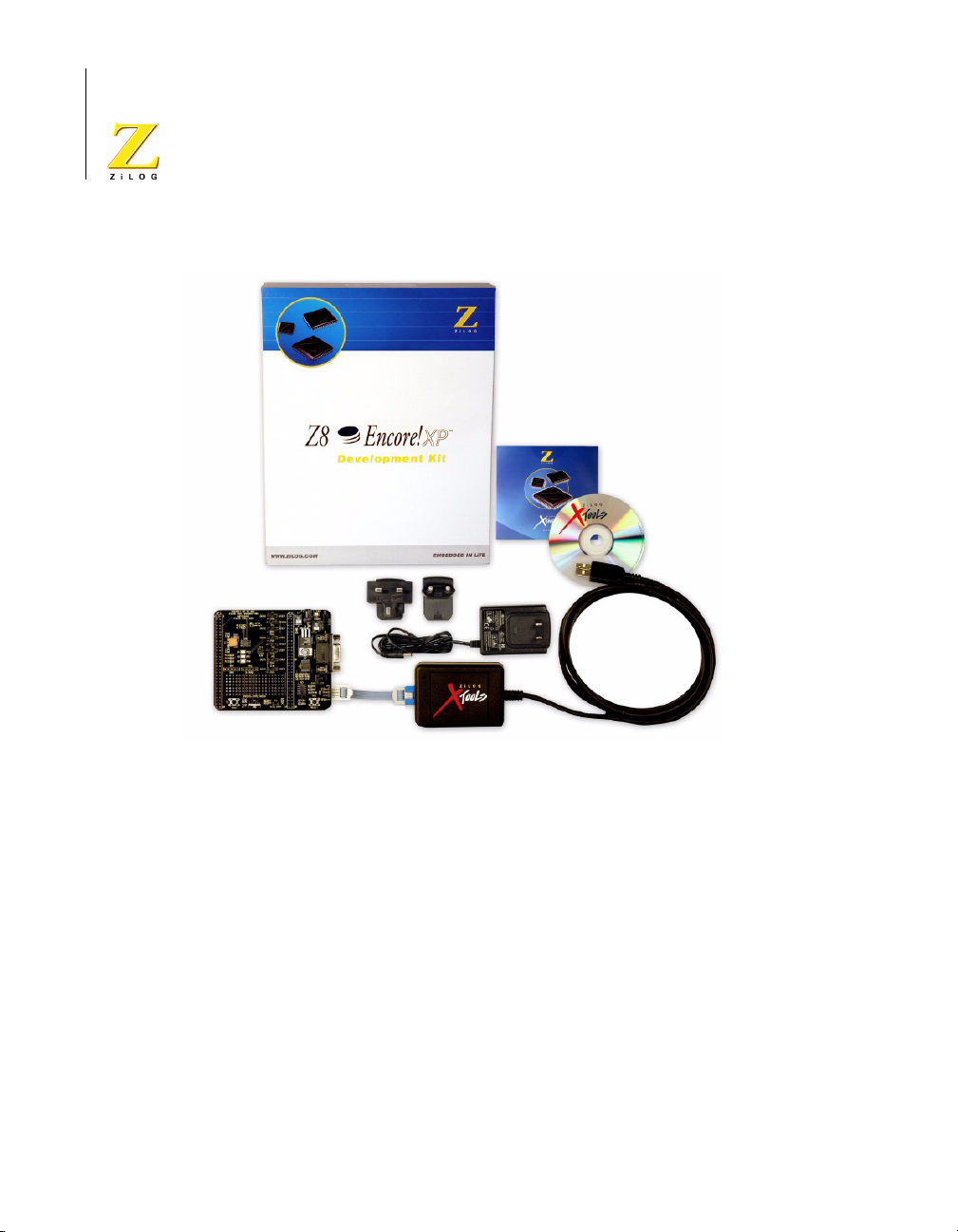
Kit Contents
The Z8 Encore! XP 4K Series 8-Pin MCU Development Kit contains the
following:
Hardware
•
Z8 Encore! XP 4K Series 8-Pin Development board
•
USB Smart Cable for PC to Z8 Encore! XP 4K Series 8-Pin Development board
•
5VDC power supply
UM018702-0505 Introduction
Page 8
Z8F04A08100KIT Development Kit
User Manual
2
Packaging
Power
Supply
CD-ROM Containing
Documentation
USB Smart Cable
Development
Board
Figure 1. Z8 Encore! XP® 4K Series 8-Pin Development Kit Contents (Printed Quick
Start Guide Not Shown)
Software (on CD-ROM)
•
ZDS II- Z8 Encore!® IDE with ANSI C-Compiler
•
Sample code
•
Document browser
•
Acrobat Reader install program
Introduction UM018702-0505
Page 9

Documentation
•
Quick Start Guide (QS0043)
•
Registration card
•
Z8 Encore! XP 4K Series 8-pin technical documentation (on CDROM)
– Development Kit User Manual
– ZDS II - IDE User Manual
– eZ8 CPU User Manual
– Application notes
Z8F04A08100KIT Development Kit
User Manual
3
The sample code is installed with ZDS II and resides in the
tion directory>\samples
The documentation can be installed by the user with the DemoShield
interface or can be viewed on the CD-ROM using the DemoShield menus
and a PDF reader. A copy of the Acrobat installer is provided on the CDROM and can be installed from the DemoShield install screen. After
installing the documentation on the user’s system Windows Explorer can
be used to select any document to be viewed with your favorite PDF file
viewer.
System/Software Requirements
IBM PC (or compatible computer) with the following minimum configurations:
Supported Host System Configuration
•
Win98 Second Edition, Win2000 Service Pack 3, WinXP Professional Service Pack 1
•
PentiumII/233MHz processor or higher up to Pentium IV, 2.8 GHz
•
96 MB RAM or more
<installa-
in the user's disk drive.
UM018702-0505 Introduction
Page 10

Z8F04A08100KIT Development Kit
User Manual
4
•
25 MB hard disk space or more
•
Super VGA video adapter
•
CD-ROM
•
One USB high-speed or full-speed port on the host chassis or a powered hub
Designing with the USB Smart Cable
The Z8 Encore! XP 4K Series 8-Pin Development Kit requires use of the
USB Smart Cable (supplied). The Z8 Encore! Serial Smart Cable and
associated TIM will not work with the Z8F04A08100KIT kit. When
designing your target board and application:
•
Your target design’s debug interface must include a RESET pin.
•
Your target application must allow the RESET pin to be pulled LOW.
Refer to the chip product specification, PS0228, for further details.
Introduction UM018702-0505
Page 11

Installation
Follow the directions in the Quick Start Guide (QS0043) for software
installation and setup of the Z8 Encore! XP 4K Series 8-Pin Development
kit.
Z8F04A08100KIT Development Kit
User Manual
5
UM018702-0505 Installation
Page 12

Z8F04A08100KIT Development Kit
User Manual
6
Installation UM018702-0505
Page 13

Development Board
Introduction
The Z8 Encore! XP® 4K Series 8-Pin Development board is a development and prototyping board for the Z8 Encore! XP 4K Series 8-Pin MCU.
The board provides customers with a tool to evaluate features of Z8
Encore! XP 4K Series 8-Pin MCU, and to start developing an application
before building the hardware.
Z8F04A08100KIT Development Kit
User Manual
7
Resonator
not installed
on production
units.
DBG
Pin 1
Figure 2. Z8 Encore! XP® 4K Series 8-Pin Development Board
UM018702-0505 Development Board
Page 14

Z8F04A08100KIT Development Kit
User Manual
8
Features
•
Z8 Encore!® MCU (8-pin SOIC)
•
3 LEDs
•
RS-232 interface
•
IrDA transceiver
•
Two pushbuttons, RESET and TEST
•
5 VDC power connector
•
On-Chip Debugger interface
•
Prototyping area
•
External interface connectors JP1 and JP2
•
2.7–3.6 V operating voltage with 5V-tolerant inputs
MCU
The Z8 Encore! XP 4K Series 8-pin MCU is member of a family of
ZiLOG microcontroller products based upon the 8-bit eZ8 core CPU. The
Flash in-circuit programming capability allows for faster development
time and program changes in the field. The eZ8 core CPU is upward compatible with existing Z8
Encore! XP 4K Series makes it suitable for a variety of applications
including motor control, security systems, home appliances, personal
electronic devices, and sensors.
The Development board contains circuitry to support and present all the
features of the Z8 Encore! XP 4K Series. The main features of the Z8
Encore! XP 4K Series 8-pin MCU are:
•
eZ8 core CPU
•
4KB Flash memory with in-circuit programming capability
Development Board UM018702-0505
®
instructions. The rich peripheral set of the Z8
Page 15

Z8F04A08100KIT Development Kit
User Manual
•
1KB register RAM
•
5-channel, 10-bit analog-to-digital converter (ADC)
•
Full-duplex UART
•
Infrared Data Association (IrDA)-compliant infrared encoder/decoder
•
Two 16-bit timers with capture, compare, and PWM capability
•
Watch-Dog Timer (WDT) with internal RC oscillator
•
Six I/O pins
•
Programmable priority interrupts
•
On-Chip Debugger
•
Voltage Brown-out Protection (VBO)
•
Power-On Reset (POR)
9
•
2.7–3.6 V operating voltage with 5V-tolerant inputs
•
Operating temperatures: 20° ±10° C
For further information on the Z8 Encore!
product specification, P/N PS0228, available for download from
www.zilog.com
.
®
family of devices, consult the
UART with IrDA Endec
The Z8 Encore! XP 4K Series 8-pin MCU (component U5) contains a
fully-functional, high-performance UART with Infrared Encoder/Decoder
(ENDEC). The Infrared ENDEC is integrated with an on-chip UART
allowing easy communication between the Z8 Encore! XP™ 4K Series 8pin MCU and IrDA transceivers. Infrared communication provides
secure, reliable, low-cost, point-to-point communication between PCs,
PDAs, cell phones, printers and other infrared enabled devices.
UM018702-0505 Development Board
Page 16

Z8F04A08100KIT Development Kit
User Manual
10
Jumpers and Settings
Table 1 provides information on jumper functions.
Table 1. Z8F04A08100KIT Jumper Functions
Jumper State Description Default
J1* OUT Enables RS-232 interface X
IN Disables RS-232 interface
J2* OUT Enables IrDA interface X
IN Disables IrDA interface
J3 1-2 Connects U5 pin PA0 to Green
LED D2
2-3 Connects U5 pin PA0 to JP2 pin 18
J4 OUT Disconnects PA0 from debug pin X
IN Connects PA0 to DBG pin 4 on ZDI
port P3.
J5 1-2 Connects U5 pin PA1 to yellow
LED D3
2-3 Connects U5 pin PA1 to JP2 pin 20
J6 1-2 Connects U5 pin PA2 to red LED
D4.
2-3 Connects U5 pin PA2 to JP2 pin 22
X
X
X
Development Board UM018702-0505
Page 17

Z8F04A08100KIT Development Kit
Table 1. Z8F04A08100KIT Jumper Functions
Jumper State Description Default
J7 OUT DEMO mode setting X
IN Chip U5 resets when SW1 pressed
J8 1-2 Connects U5 pin PA3 to J11 pin 1
(CTS0 EN)
2-3 Connects U5 pin PA3 to JP2 pin 35
J9 1-2 Connects U5 pin PA4 to RXD
RS232 signal
2-3 Connects U5 pin PA4 to JP2 pin 35
J10 1-2 Connects U5 pin PA5 to TXD
RS232 signal
2-3 Connects U5 pin PA5 to JP2 pin 36
J11 OUT Disconnects PA3 from CTS0
RS232 signal
IN Connects PA3 to CTS0 RS232
signal
Note: * These jumpers must not be OUT at the same time
User Manual
11
X
X
X
X
The board has two modes of operation: DEMO and USER. Use DEMO
mode to run the sample program included with the kit. Run the board in
USER mode:
•
When using the ZDI port to debug your code.
•
When configuring the board to run your own prototype code.
DEMO Mode Jumper Settings
When running the board in DEMO mode, the following jumpers MUST
be set:
UM018702-0505 Development Board
Page 18

Z8F04A08100KIT Development Kit
User Manual
12
J3 1-2
J4 OUT
J5 1-2
J6 1-2
J7 OUT
J8 1-2
J9 1-2
J10 1-2
J11 OUT
USER DEBUG Mode Jumper Settings
When running the board in USER DEBUG mode, the following jumpers
MUST be set:
J3 OUT
J4 IN
J6 OUT
J7 IN
Switches S1, S2, and SW1
Switches S1, S2, and SW1 on the Z8 Encore! XP™ 4K Series 8-Pin
Development board perform the following functions:
•
S1 – Test switch
•
S2 – Power ON/OFF switch
•
SW1 – RESET
External Interface Headers JP1 and JP2
External interface headers JP1 and JP2 are shown in the schematic on
page 15.
Development Board UM018702-0505
Page 19

Use of Ceramic Resonator Y1
When using ceramic resonator Y1, pins PA0, PA1, and DBG are unavailable to the user. For more information, refer to the Z8 Encore! XP™ 4K
Series Product Specification, PS0228.
Z8F04A08100KIT Development Kit
User Manual
13
UM018702-0505 Development Board
Page 20

Z8F04A08100KIT Development Kit
User Manual
14
Development Board UM018702-0505
Page 21

Schematic
This section includes schematics for the Z8 Encore! XP 4K Series 8-Pin
Development Board.
Z8F04A08100KIT Development Kit
User Manual
15
UM018702-0505 Schematic
Page 22

Z8F04A08100KIT Development Kit
User Manual
16
UM018702-0505 Schematic
Page 23

Z8F04A08100KIT
User Manual
P1
PWR JACK
GND
GND
VCC_33V
2
3
1
R3
0
R4
0
R8
0
R9
0
S2
ON
F
OF
SW KEY-SPDT
VCC_33V
147
3 4
GND
VCC_33V
147
5 6
GND
VCC_33V
147
11 10
VCC_33V
147
13 12
U3B
74LVC04/SO
U3C
74LVC04/SO
U3E
74LVC04/SO
GND
U3F
74LVC04/SO
GND
U2
3 2
VIN
VOUT
1
GND
SPX2815AU-3
.3
GND
TXD0
CTS0
RXD
0
C9
330nF
U4
5
VCC
1
LEDA
2
TXD
4
SD
3
RXD
6
GND
0964-001
C1
0.1uF
CONSO
P2
1
6
2
7
3
8
4
9
5
DB9 Female
USER
T
ZHX181
0
Sheet
12
LE
0
of
1918
D0
13
12
15
0
10
20
147
9 8
2
4
5
6
1
-RESE
DBG
U1
C1+
C1C2+
C2-
T1IN
T2IN
R1OUT
R2OUT
EN
SHDN
U3D
74LVC04/SO
T
3
V+
VCCGND
7
V-
17
T1OUT
8
T2OUT
16
R1IN
9
R2IN
14
NC
11
NC
SP3222EBCA
GND
Title
SizeDocument Number
Date:
XP 4K 8 pin MD
B
Tuesday, December 14, 2004
C5
0.1uF
R5
68
R6
2R7
PA5_TX
D0
IRDA_SD
PA4_RXD
0
S Processor Module. Schematic.
96C
C2
PA5_TX
D0
0
147
1 2
R7
10K
E
-RESET
DBG
0.1uF
C6
0.1uF
GND
PA4_RXD
U3A
74LVC04/SO
VCC_33V
GND
R10
10K
5V
C4
0.1uF
0.1uF
C8
TP1
+
C3
10/6
12345
GND
10/6
VCC
+
J11
HEADER 2
VCC_33V
VCC_33V
R1
C7
68
LED
21
GND
0
D1
3.3 OK
TP
2
PA3_CTS
VCC_33V
12345
0
PA3_CTS
VCC_33V
GND
0
CTS0
VCC_33V
-DIS_232
R2
10K
1
2
EN
J1
1
2
DIS RS
-DIS_IRDA
J2
DIS IR
P3
12
34
56
Header 3x2
PA5_TX
PA4_RXD
GND
232
1
2
DA
DBG
INTERFAC
17
Rev
B
UM018702-0505
Schematic, Z8 Encore! XP™ 4K Series 8-Pin MCU Development Board, Page 1 of 2
Page 24

Z8F04A08100KIT
User Manual
PA0_JP
PA1_JP
R17
0
R19
0
VCC_33VVCC_33VVCC_33VVCC_33VVCC_33VVCC_33V
R12
10K
S1
1 2
TES
VCC_33V
PA0
PA1
PA2_JP
R21
220K
Y1
1
1
2
2
TABLE
3
20 MHz
3
1
T
PA3_CTS
0
C13
8 pin foot
print
U5
VSS
VDD
2 7
PA0 PA5
3
PA1
PA4
4
PA2
PA3
Z8F04xA_8pin
R20
0
C11
NOTE
2
81
PA5_JP
PA4_JP
6
PA3_JP
5
VCC_33V
GND
R16
0
C10
Clock Mode R16 R17 R19 R20
Internal Note 2 Note 2 none none no
Ceramic Res none none 0 Ohm 0 Ohm 22
Crystal none none 0 Ohm 0 Ohm 22
GND
R11
10
0
R13
10
0
R15
10
0
D2
2 1
LED
D3
2 1
LED
D4
2 1
LED
PA3_CTS
0
PA4_RXD
0
PA5_TX
D0
R21 C10 C11 Y1
ne none none none
0K 10-20pF 10-20pF user
select
0K 10-20 pF 10-20 pF user
select
LED_G
DEMO USER
GREEN
LED_Y
DEMO USER
YEL
LED_R
RED
DEMO USER
PA3_CTS
0
DEMO USER
PA4_RXD
0
DEMO USER
PA5_T
XD0
PA0_JP
PA1_JP
PA2_JP
PA3_JP
PA4_JP
PA5_JP
123
Header 3
PA0
123
Header 3
123
Header 3
123
Header 3
123
Header 3
123
Header 3
PA0_MDS
J3
J4
PA1
PA2
J5
J6
J8
PA3
J9
PA4
1
2
HEADER 2
PA1_MDS
PA2_MDS
J7
HEADER 2
PA3_MDS
PA4_MDS
PA5_MDS
DBG
DBG
1
2
RESET
USERDEMO
J10
PA5
Note 2:
The XP supports internal oscillator, extern
resonator, external R/C and external CMOS dr
R17, R19, R20, R21, C10, C11 and Y1 are used to
selected. The development board is shipped c
oscillator. When using internal oscilator, p
as GPIO ports PA0 and PA1. Table 1 shows th
configurati
ons.
Note
1:
If Module is plugged onto the De
RS232 interface is disabled
VCC_33V
SW1
GND
RESET
-RESET
al crystal, or ceramic
ive clock modes. R16,
support the clock mode
onfigured for internal
ins 2 and 3 could be used
e recommended clock mode
R14
10K
v Platform the local
by pin 50 of JP2
VCC_33V
GND
PA3_MDS
PA4_MDS PA5_MDS
GND
-RESET-RESE
VCC_33V
Title
XP 4K 8pin
SizeDocument Number
B
Tuesday, December 14, 2004
Date:
JP2
connecto
2
1
4
3
6
5
8
7
9
11
13
15
17
19
21
23
25
27
29
31
33
35
37
39
41
43
45
47
49
51
T
53
55
57
VCC_33V
59
HEADER 30x2/SM
Connector
for referen
GND
10
12
14
16
PA0_MDS
18
PA1_MDS
20
PA2_MDS
22
24
26
28
30
32
34
36
38
40
42
44
46
48
50
-DIS_IrDA
52
54
56
58
60
JP1
ce
only
JP1
2
1
4
3
-TRS
TN
-F91_WE
GND
A6 A0
11
A10
13
GND
15
A8
17
A13
19
A15
21
23
A19
25
27
A11
29
A4
31
A5
33
35
A21
37
A22
39
-CS0
41
-CS2
43
D1
45
D3
47
D5
49
D7
51
-MREQ
-WR
-BUSACK
53
55
57
59
GND
MDS Processor Module. Schematic.
96C
0964-001
5
7
9
HEADER 30x2/SM
6
8
10
12
14
16
18
20
22
24
26
28
30
32
34
36
38
40
42
44
46
48
50
52
54
56
58
60
Sheet
VCC_33V
A3
VCC_33V
A7
A9
A14
A16A18
GND
A1A2
A12
A20
A17
-DIS_FLASH
VCC_33V
A23
-CS1
D0
D2
D4
GND
D6
-IOREQ
-RD
-INSTRD
-BUSREQ
r 2
GND
GND
-DIS_232
-DIS_IRDA
GND
Rev
B
of
22
18
UM018702-0505
Schematic, Z8 Encore! XP™ 4K Series 8-Pin MCU Development Board, Page 2 of 2
 Loading...