

Page 1
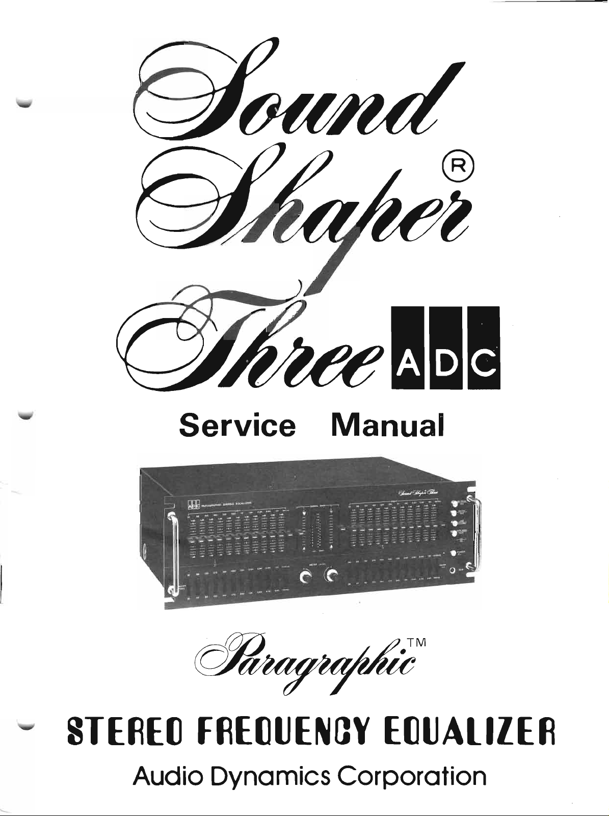
Service Manual
STE~E() F~E()UEN(]Y
Audio Dynamics Corporation
E()UALllEfl
Page 2
~---------------CONTENTS----------------~
PAGE
ELECTRICAL PERFORMANCE SPECIFICATIONS 3
CI RCUIT DESCRiPTION , 4-9
SWITCH FUNCTIONS 0-12
DISASSEMBLY INSTRUCTIONS 2
BLOCK DIAGRAM .
ADJUSTMENT PROCEDURES '-
CALIBRATOR SCHEMATIC.................................. . . . . .. .. -
TROUBLESHOOTING - SYMPTOM· CAUSE/REMEDY
AMP P. C. B. (TOP
POWER SUPPLY
SWITCH (L) P. c. B. (TOP
SWITCH (R) P.
SLIDE VOLUME (L) P.
SLIDE VOLUME (R) P. C. B. (TOP&BOTTOM VIEWS)
ELECTRICAL PARTS LIST
EXPLODED VIEW PARTS LIST 35-36
MISCELLANEOUS PARTS LIST 37
SCHEMATIC DIAGRAM
EXPLODED VIEW
&
BOTTOM VI EWS) . . . . . . . . . . . . . . . . . . . . . . . . . . . . . . . . . .. ~
&
METER P. C. B. (TOP
&
BOTTOM VIEWS) 21
c.
B. (ROP
&
c.
B. (TOP
&
BOTTOM VI EWS) ~
BOTTOM VIEWS) 22
&
BOTTOM VIEWS)
i7- ':'
23
24
25-34
38-39
40-41
-2-
Page 3
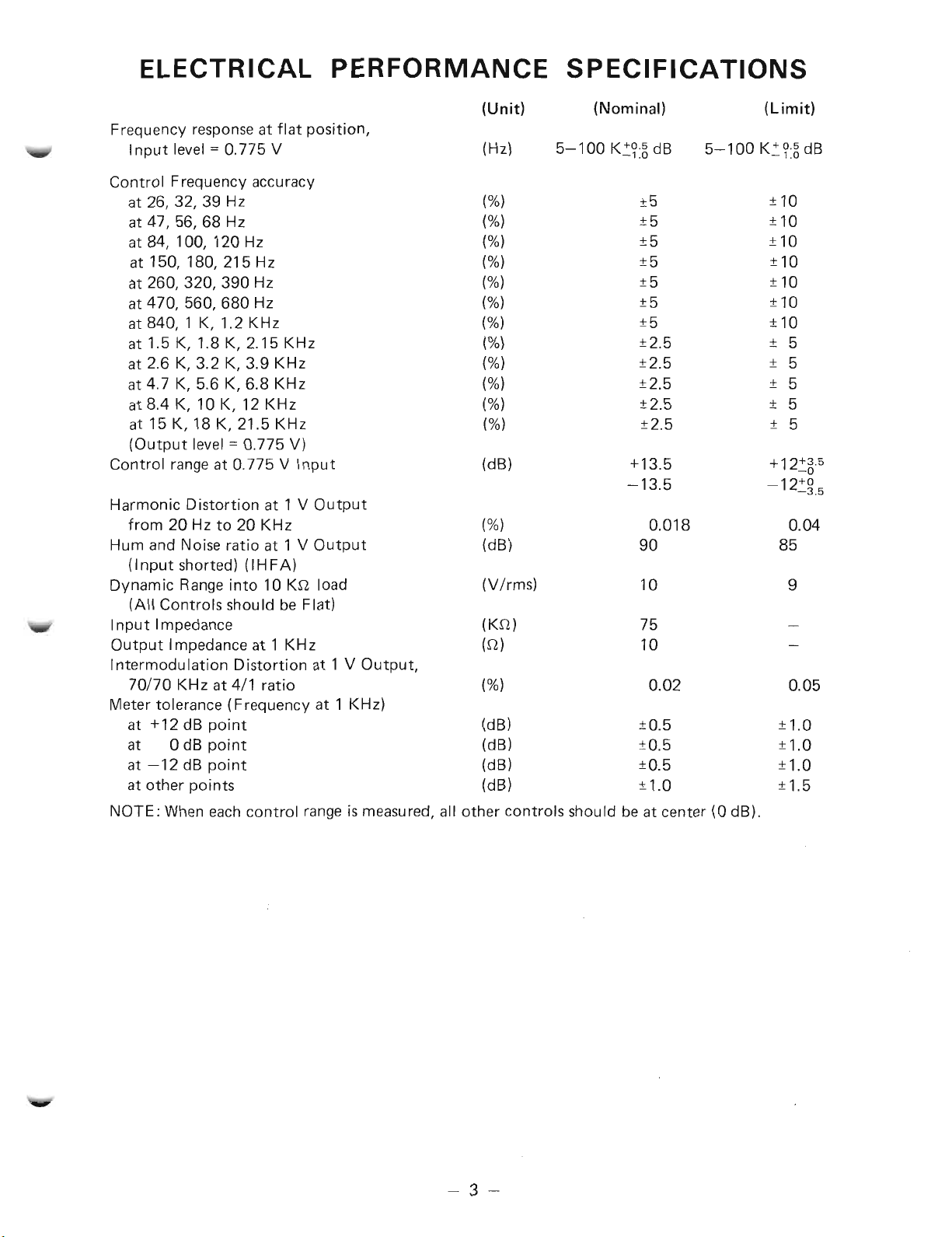
ELECTRICAL
PERFORMANCE
SPECIFICATIONS
(Unit)
(Nominal)
(Limit)
Frequency response at flat position,
Input level
=
0.775 V
(Hz)
5-100 K~U dB
5-100 K~?:5 dB
Control Frequency accuracy
at 26, 32, 39 Hz
at 47, 56, 68 Hz
at 84,100,120 Hz
at 150,180,215 Hz
at 260,320,390 Hz
at 470, 560, 680 Hz
at 840, 1 K, 1.2 KHz
at 1.5 K, 1.8 K, 2.15 KHz
at 2.6 K, 3.2 K, 3.9 KHz
at 4.7 K, 5.6 K, 6.8 KHz (%)
at 8.4 K, 10 K, 12 KHz
at 15 K, 18 K, 21.5 KHz
=
(Output level
0.775 V)
Control range at 0.775 V Input
(%)
(%)
(%)
(%)
(%)
(%)
(%)
(%)
(%)
(%)
(%)
(dB)
±5 ±10
±5
±5
±5
±5
±5
±5
±2.5 ±
±2.5
±2.5 ±
±2.5 ±
±2.5 ±
+13.5
-13.5
-12~~.5
Harmonic Distortion at 1 V Output
from 20 Hz to 20 KHz
Hum and Noise ratio at 1 V Output
(%)
(dB)
0.018
90
(I nput shorted) (I HFA)
Dynamic Range into 10 Kn load
(V/rms)
10
(All Controls should be Flat)
Input Impedance (Kn) 75
Output Impedance at 1 KHz (n) 10
Intermodulation Distortion at 1 V Output,
70/70 KHz at 4/1 ratio (%) 0.02 0.05
Meter tolerance (F requency at 1 KHz)
at+12dBpoint (dB) ±0.5 ±1.0
at OdBpoint (dB) ±0.5 ±1.0
at-12dBpoint (dB) ±0.5 ±1.0
at other points (dB) ± 1.0 ± 1.5
±10
±10
±10
±10
±10
±10
5
±
5
5
5
5
+12~~·5
0.04
85
9
NOTE: When each control range is measured, all other controls should be at center (0 dB).
- 3 -
Page 4
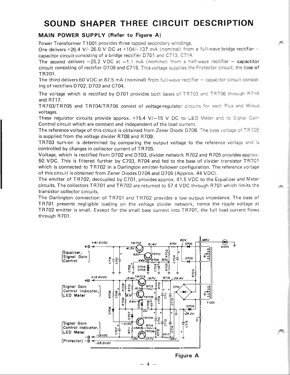
SOUND SHAPER THREE CIRCUIT DESCRIPTION
MAIN POWER SUPPLY (Refer to Figure A)
Power Transformer T 1001 provides three tapped secondary windings.
i
One delivers +26.4 V /- 26.0 V DC at +104/-137 rnA (no
capacitor circuit consisting of a bridge rectifier D701 and C73,C7
The second delivers -25.2 VDC at -1.1 rnA (nominal)
circuit consisting of rectifier D709 and C715. This voltage supplies - e
TR201.
The third delivers 60 VDC at 87.5 mA (nominal) from full-wave
ing of rectifiers D702, D703 and C704.
all fro
fro a
rectifi
a full-wave bridge rectifier -
4.
e roc"ifier - cspactitor
- CI
cireui , e base of
co
The voltage which is rectified by D701 provides both bases of TR703
andR717.
TR703/TR705 and TR704/TR706 consist of voltage-regulator circuits 'or
voltages.
These regulator circuits provide approx. +15.4 V /-15 V DC to LED Meter ana 5"
Control circuit which are constant and independent of the load current.
The reference voltage of this circuit is obtained from Zener Diode D708. The base voltage of T
is supplied from the voltage divider R708 and R709.
TR703 turn-on is determined by comparing the output voltage to the reference voltage and is
controlled by changes in collector current of TR705.
Voltage, which is rectified from D702 and D703, divider network R702 and R705 provides approx.
50 VDC. This is filtered further by C703, R704 and fed to the base of divider transistor TR701
which is connected to TR702 in a Darlington emitter-follower configuration. The reference voltage
of this circuit is obtained from Zener Diodes D704 and D705 (Approx. 44 VDC).
The emitter of TR702, decoupled by C701, provides approx. 41.5 VDC to the Equalizer and Meter
circuits. The collectors TR701 and TR702 are returned to 57.4 VDC through R701 which limits the
transistor collector circuits.
The Darlington connection of TR701 and TR702 provides a low output impedance. The base of
TR701 presents negligible loading on the voltage divider network, hence the ripple voltage at
TR702 emitter is small. Except for the small base current into TR701, the full load current flows
through R701.
c T
- 4 -
Figure A
Page 5
LED METER COMPARATOR CIRCUIT DESCRIPTION
Power Supply and bias configuration (Refer to LED METER circuits)
The power supply for the LED Meter Comparator circuit consists of full-wave rectifiers, which
provide plus (+) and minus (-) +15.4/-15 VDC to each of IC802 through IC814.
LED indication level is provided from the Zener diode D71 0 (-5.6 VDC).
The +15.4/-15 VDC source is applied to LED comparator ICs IC802 through IC814.
The -5.6 VDC source provides a stable voltage to VR801 (L) and VR802 (R) for LED Meter
indicator level.
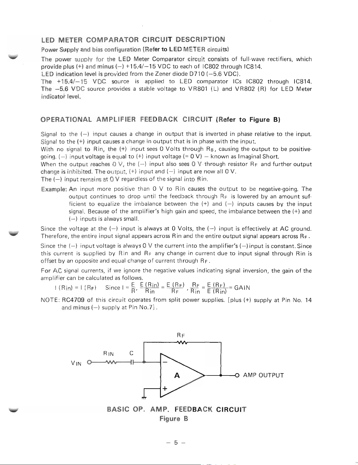
OPERATIONAL AMPLIFIER FEEDBACK CIRCUIT (Refer to Figure B)
Signal to the (-) input causes a change in output that is inverted in phase relative to the input.
Signal to the (+) input causes a change in output that is in phase with the input.
With no signal to Rin, the (+) input sees 0 Volts through RB, causing the output to be positivegoing. (-) input voltage is equal to (+) input voltage
When the output reaches 0 V, the (-) input also sees 0 V-through resistor RF and further output
change is inhibited. The output, (+) input and (-) input are now all 0 V.
The (-) input remains at 0 V regardless of the signal into Rin.
Example: An input more positive than 0 V to Rin causes the output to be negative-going. The
output continues to drop until the feedback through RF is lowered by an amount sufficient to equalize the imbalance between the (+) and (-) inputs causes by the input
signal. Because of the amplifier's high gain and speed, the imbalance between the (+) and
(-) inputs is always small.
(=
0 V) - known as I maginal Short.
Since the voltage at the (-) input is always at 0 Volts, the (-) input is effectively at AC ground.
Therefore, the entire input signal appears across Rin and the entire output signal appears across R
Since the (-) input voltage is always 0 V the current into the amplifier's (-) input is constant. Since
this current is supplied by Rin and RF any change in current due to input signal through Rin is
offset by an opposite and equal change of current through RF .
For AC signal currents, if we ignore the negative values indicating signal inversion, the gain of the
amplifier can be calculated as follows.
I (Rin)
NOTE: RC4709 of this circuit operates from split power supplies. [plus (+) supply at Pin No. 14
=
I (RF) Since
and minus (-) supply at Pin No.7].
1=
g_
E (Rin)=E (RF)
R'
Rin RF' Rin E (Rin)
__B__E
=
E (RF) GAIN
AMP OUTPUT
F •
BASIC OP. AMP. FEEDBACK CIRCUIT
Figure B
- 5 -
Page 6
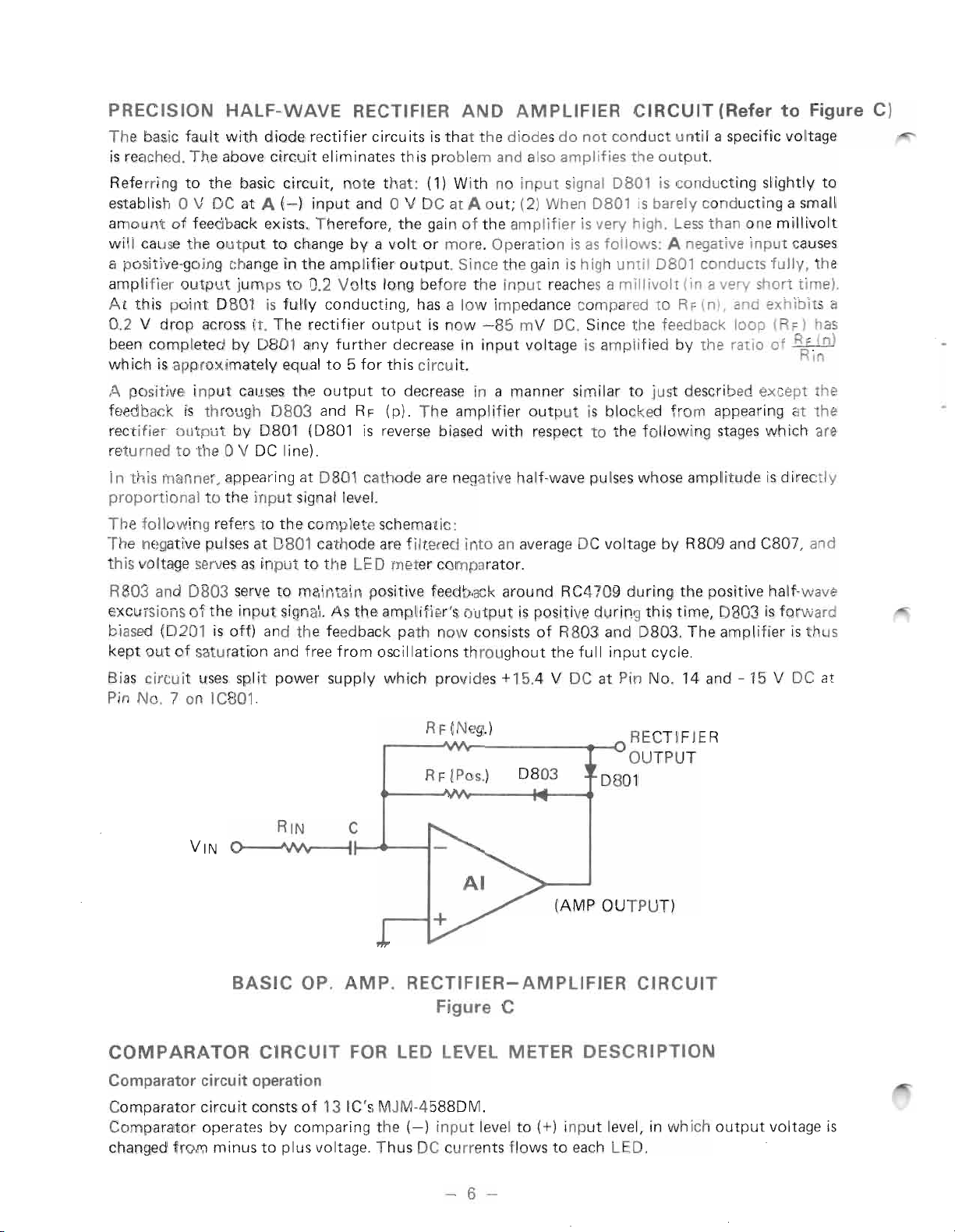
PRECISION HALF-WAVE RECTIFIER AND AMPLIFIER CIRCUIT (Refer to Figure C)
The basic fau It with diode rectifier circu its is that the diodes do not conduct until a specific voltage
is reached. The above circuit eliminates this problem and also amplifies the output.
Referring to the basic circuit, note that: (1) With no input signal 0801 is conducting slightly to
establish 0 V DC at
amount of feedback exists. Therefore, the gain of the amplifier is very high. Less than one millivolt
will cause the output to change by a volt or more. Operation is as follows:
a positive-going change in the amplifier output. Since the gain is high until 0801 conducts fully, the
amplifier output jumps to 0.2 Volts long before the input reaches a millivolt (in a very short time).
At this point 0801 is fully conducting, has a low impedance compared to RF (n), and exhibits a
0.2 V drop across it. The rectifier output is now -85 mV DC. Since the feedback loop (RF) has
been completed by 0801 any further decrease in input voltage is amplified by the ratio of RR'.(n)
which is approximately equal to 5 for this circuit.
A positive input causes the output to decrease in a manner similar to just described except the
feedback is through 0803 and RF (p). The amplifier output is blocked from appearing at the
rectifier output by 0801 (0801 is reverse biased with respect to the following stages which are
returned to the 0 V DC line).
In this manner, appearing at 0801 cathode are negative half-wave pulses whose amplitude is directly
proportional to the input signal level.
The following refers to the complete schematic:
The negative pulses at 0801 cathode are filtered into an average DC voltage by R809 and C807, and
this voltage serves as input to the LED meter comparator.
A (-)
input and 0 V DC atAout; (2) When 0801 is barely conducting a small
A
negative input causes
In
R803 and 0803 serve to maintain positive feedback around RC4709 during the positive half-wave
excursions of the input signal. As the amplifier's output is positive during this time, 0803 is forward
biased (0201 is off) and the feedback path now consists of R803 and 0803. The amplifier is thus
kept out of saturation and free from oscillations throughout the full input cycle.
Bias circuit uses split power supply which provides +15.4 V DC at Pin No. 14 and -15 V DC at
Pin NO.7 on IC801.
r-_R_F-"/V(N"y-e_g_.)
R F (Pos.)
----.--0
0803
(AMP OUTPUT)
RECT I FIE R
OUTPUT
0801
BASIC OP. AMP. RECTIFIER-AMPLIFIER CIRCUIT
Figure C
COMPARATOR CIRCUIT FOR LED LEVEL METER DESCRIPTION
Comparator circuit operation
Comparator circuit consts of 13 IC's MJM-4588DM.
Comparator operates by comparing the (-) input level to (+) input level, in which output voltage is
changed from minus to plus Voltage. Thus DC currents flows to each LED.
- 6 -
Page 7
With no signal, (-) input level [No.2 (L) or No.6 (R)1is kept to 0 V DC.
(+) input level [Pin NO.3 (L) or Pin No.5 (R)l of IC814 is kept to minus DC voltage (about
-45 mV) by half-wave rectifiers through VR801 (L) [VR802 (R)l and VR805 (L) [VR806
Thus, the output voltage of IC814 [Pin No.1 (L) or No.7 (R)1is kept with minus DC voltage.
When minus DC voltage is applied to (-) input, and causes the (-) input voltage to be greater (or
equal) to the (+) input voltage, the output appears as plus DC voltage. (V3:s. V2)
Thus LED D925 (L) and D926 (R) are lit at -12 dB points. But D901 through D924 are not lit
because the input voltage is too low.
Each LED conducts with a (-) input level which is determined by VR801 (L), VR802 (R) (IC802),
R813 (L), R814 (R) (IC803), R817 (L). R818 (R) (IC804), R821 (L), R822(R) (IC805), R825(L),
R826 (R) (IC806), R829 (L), R830 (R) (IC807), R833 (L), R834 (R) (IC808), VR803 (L), VR804
(R) (IC809), R839 (L), R840 (R) (IC810), R843 (L), R844 (R) (IC811), R847 (L), R848 (R)
(IC812), R851 (L), R852 (R) (IC813), R855 (L), R856 (R) (IC814).
With an increase in minus DC voltage, provided to the (-) input, each LED is lit in sequence from
D923, D924 to D901, D902.
mn
CIRCUIT DESCRIPTION
FREQUENCY EQUALIZATION
The input signal is fed into TR101 base. TR101, an emitter follower, provides the high input im-
pedance required by the signal source. The low output impedance of TR101 is required to drive
a voltage divider formed by R 111 and the sections of the frequency control pots between the cut
end of each control and its wiper. The wiper of each control effectively qrounds only those free
quencies resonated by the series traps (coil, capacitor and resistor from wiper to common). Thus,
the voltage division which occurs can be different for each frequency and depends on the frequency
control settings.
TR103, TR105 and TR107 are connected so that the voltage at TR105 base always follows the
voltage at T R 103 base. For example: An increase in voltage at TR 103 base causes the conduction of
TR 103 and TR 107 to increase, and feedback base drive of TR 105 to increase, until the voltage at
TR105 base is equal to that at TR103 base. Conduction cannot increase beyond this point since
the emitter voltage supplied by TR105 then tends to make TR103 conduct less. Conversely, a de-
crease in voltage at T R 103 base causes a corresponding change at T R 105 base.
The output voltage is taken from TR107 collector and is also fed back to TR105 base through the
voltage divider formed by R 115 and the sections of the frequency control pots between the boost
end of each control and its wiper.
For each frequency, moving the control pot off center towards boost causes an increase in the
amplitude of the signal presented to TR103 base and a decrease in the negative feedback to TR105
base. The gain is thus increased. Since the signal amplitudes at the bases of T R 103 and T R 105 are
always equal, the output signal divided by the feedback attenuation (R 115 and boost sections) is
approximately equal to the input signal amplitude divided by the input attenuation (R 111 and
"CUT" sections). By following a similar line of thought, it will be seen that when the controls are
centered the gain is unity; and when the controls are towards cut, the gain is less than one.
The resistors in series with the series resonant circu its are used to increase the bandwidth or lower
"Q",
the
viding a smooth overall response. The resistors are of different values so that the total series
resistance of each circuit (coil and resistor) is approximately the same. The ratio of the total series
resistance of the resonant circuit to the base resistor of TR 103 and TR 105 determines the maximum
boost or cut obtainable.
of each circuit so that the effect of controls of adjacent frequencies overlap, thus pro-
- 7 -
Page 8
SIGNAL GAIN CONTROL CIRCUIT
Signal Gain Control circuit consists of T R109, 111, 113 and 115 (L ch) and TR 110, 112, 114 and
116(Rch).
This circuit configuration is identical to the Frequency Equalization circuit. For operating, see
"Frequency Equalization description" section.
The input signal is fed into TR 109 base.
TR111, TR113 and TRl15 are connected so that the voltage at TR105 base always follows the
voltage at T R 111 base.
Total gain can vary from negative feedback value which consists of R135, VR101 and R143 (L ch)
[R136, VR102 and R144 (R ch)].
When base voltage of T R 111 is equal to base voltage of TR 113, the gain is unity.
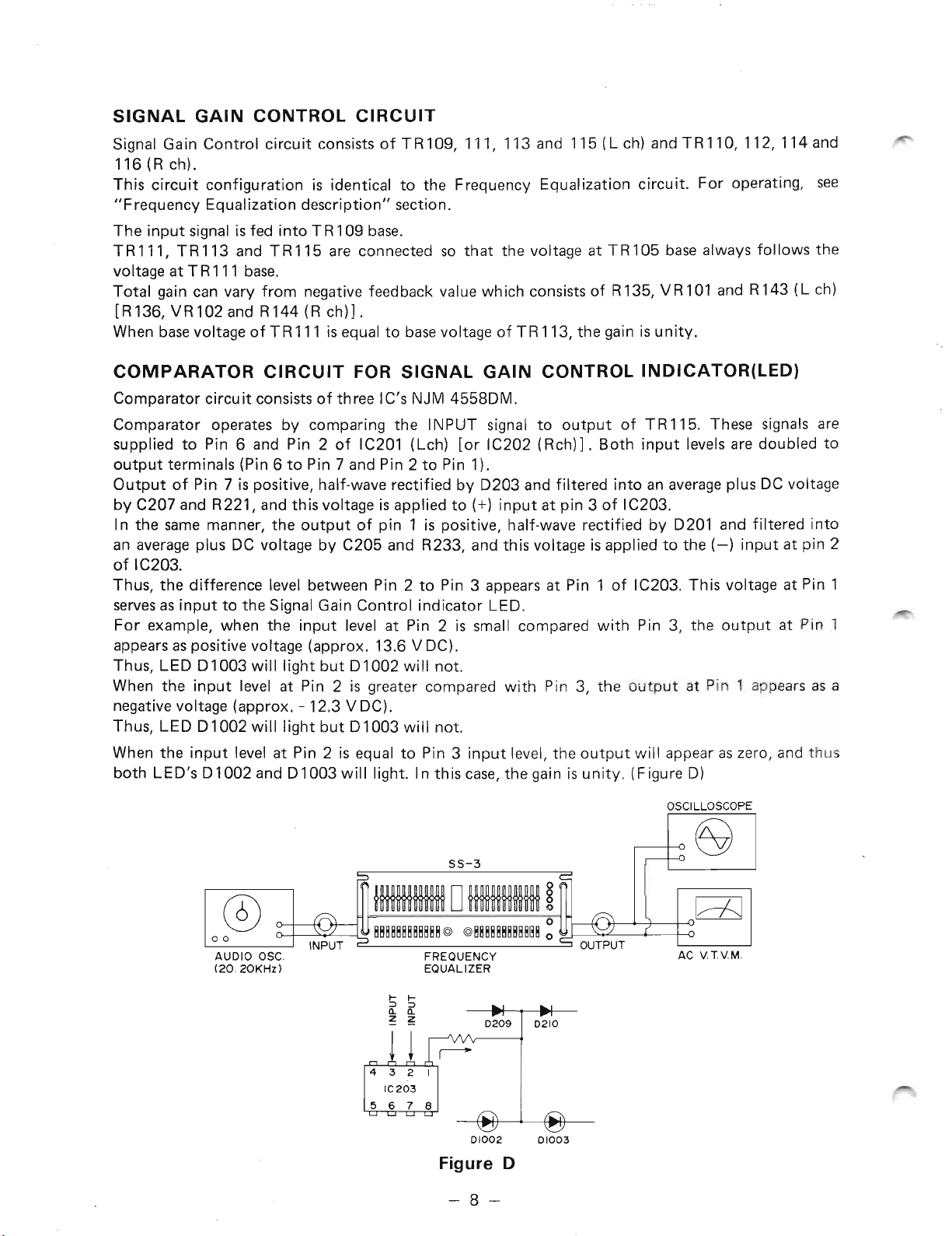
COMPARATOR CIRCUIT FOR SIGNAL GAIN CONTROL'INDICATOR(LED}
Comparator circuit consists of three IC's NJM 4558DM.
Comparator operates by comparing the INPUT signal to output of TR 115. These signals are
supplied to Pin 6 and Pin 2 of IC201 (Lch) [or IC202 (Rch)] . Both input levels are doubled to
output terminals (Pin 6 to Pin 7 and Pin 2 to Pin 1).
Output of Pin 7 is positive, half-wave rectified by D203 and filtered into an average plus DC voltage
(+)
by C207 and R221, and this voltage is applied to
In the same manner, the output of pin 1 is positive, half-wave rectified by D201 and filtered into
an average plus DC voltage by C205 and R233, and this voltage is applied to the (-) input at pin 2
of IC203.
Thus, the difference level between Pin 2 to Pin 3 appears at Pin 1 of IC203. This voltage at Pin 1
serves as input to the Signal Gain Control indicator LED.
For example, when the input level at Pin 2 is small compared with Pin 3, the output at Pin 1
appears as positive voltage (approx. 13.6 V DC).
Thus, LED D1003 will light but D1002 will not.
When the input level at Pin 2 is greater compared with Pin 3, the output at Pin 1 appears as a
negative voltage (approx. -12.3 V DC).
Thus, LED D1002 will light but D1003 will not.
input at pin 3 of IC203.
When the input level at Pin 2 is equal to Pin 3 input level, the output will appear as zero, and thus
both LED's D1002 and D1003 will light. In this case, the gain is unity. (Figure D)
OSCILLOSCOPE
f--o
~
[1]
Po
SS-3
c::=
o
o
0
AUDIO OSC. FREQUENCY AC V.TV.M.
(20. 20KHz) EQUALIZER
o-+--©-
INPUT OUTPUT
MH 0 illiMMIIlII
::>
BBBBBBBBBBBB @ @BBBB88BBB888 ~
I- I-
:;)
:;)
Q. Q.
Z ~ 0209 0210
01002 01003
§
c:::;
----@
,---
f
Figure D
-8-
Page 9

POPPING NOISE PROTECTIVE CIRCUIT
This circuit eliminates the popping noise in the speakers when the power switch is turned "on" or
II
off".
This circuit consists of TR201, TR202, TR203 and a Reed Relay.
When power is switched "on", -0.5 VDC is provided to the base of TR201 through R238. TR201
will turn off. After about 6 seconds, TR202, TR203 will turn on. Thus the Reed Relay will restore
connections to the OUTPUT Terminals.
When the power switch is "off", 1.7 VDC is provided to the baseof TR201 through R237. TR201
will turn on, TR202 and TR203 will turn off. And thus the Reed Relay will disconnect the
OUTPUT.
LED METER OPERATING CHART
AC INPUT AT VR301
(Max. CW)
mV RMS @ 1 KHz
See NOTE 1.
12 mV
15 mV
19 mV
24 mV
29 mV
35mV
46 mV
65 mV
74 mV
100 mV
120 mV
150 mV
190 mV
RECTIFIED DC V
AT C807 (-) INDICATION CURRENT EACH LED
See NOTE 2. See NOTE 3.
-53 mV DC -12 dB
-76 mV DC -10dB
-102 mV DC
-132 mV DC -6 dB
-166 mV DC -4dB
-205 mV DC
-278 mV DC OdB 2.63 mA
-395 mV DC +2 dB 2.63 mA 1.84 V DC
-453 mV DC
-618 mV DC
-740 mV DC +8dB 2.63 mA
-940 mV DC +10 dB
-1.18 V DC
LED METER LED METER
(mA)
2.63 mA
2.63 mA 1.84 V DC
-8dB
2.63 mA 1.84 V DC
2.63 mA
2.63 mA
-2dB
+4 dB
+6 dB
2.63 mA
2.63 mA
2.63 mA
2.63 mA
+12 dB
2.63 mA
VOLTAGE ACROSS
DC VOLTS
1.84 V DC
1.84 V DC
1.84 V DC
1.84 V DC
1.84 V DC
1.84 V DC
1.84 V DC
1.84 V DC
1.84 V DC
1.84 V DC
Rectified DC V and LED Meter data for actual levels used for LED Meter indication. (LED "ON"
condition)
NOTE:
1. AC signal applied to INPUT jacks of Equalizer.
BY-PASS/EO switch to EO, METER switch to IN, LINE/REC to REC and MONITOR to OUT.
2. Rectified DC voltages measured from C807 (-).
3. Indicated voltages across each LED indicator are obtained with LED Meters calibrated as
specified in the CALIBRATOR PROCEDURE section of this manual.
±
4. All DC voltages are within
10%, measured with AC\ VTVM and DC Voltmeter (over 10 Kn/V).
l
- 9 -
Page 10
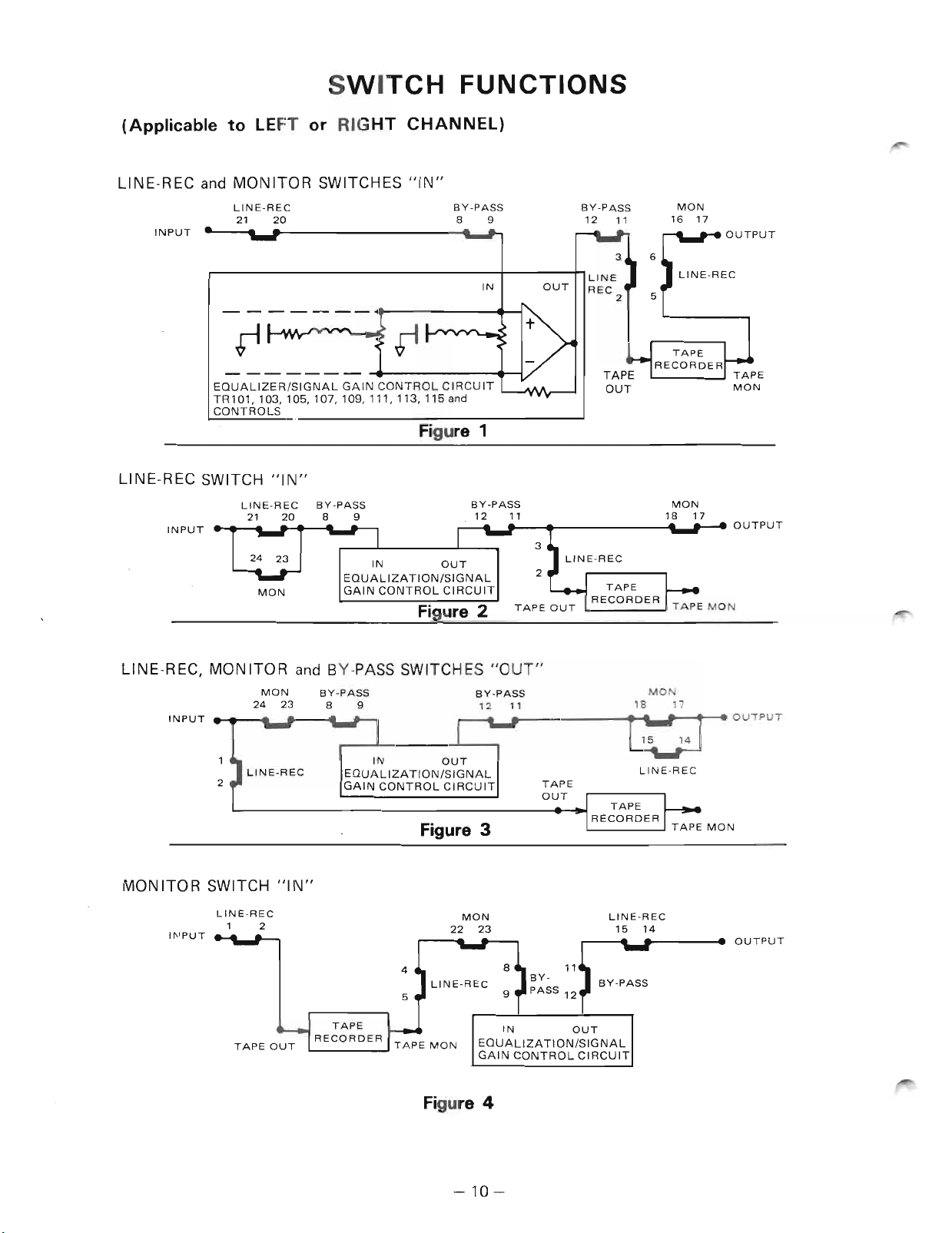
SWITCH FUNCTIONS
(Applicable to LEFT or RIGHT CHANNEL)
LlNE-REC and MONITOR SWITCHES "IN"
INPUT
LlNE-REC
21 20
- - - - ~ - - .....--------41~
BY-PASS
8 9
IN lOUT
BY-PASS
12 11
MaN
16 17
~
--------
EQUALIZER/SIGNAL GAIN CONTROL CIRCUIT
TR101,103,10S,107,109,111,113,11Sand
CONTROLS
p
L-AAA___J
Figure 1
LI NE-REC SWITCH "IN"
BY-PASS
12 11
~ • • •• OUTPUT
INPUT
LlNE-REC BY-PASS
21 20
24 23
MaN
8- 9
EQUALIZATION/SIGNAL
GAIN CONTROL CIRCUIT
IN OUT
Figure 2
LI NE-REC, MON ITO R and BY -PASS SWITCH ES "OUT"
INPUT
2
MaN
24 23
LlNE-REC
BY-PASS
8 9
IN OUT
EQUALIZATION/SIGNAL
GAIN CONTROL CIRCUIT
BY-PASS
12 11
~ r'
_/
7
TAPE
OUT
LlNE-REC
i ·
MaN
OUTPUT
MONITOR SWITCH "IN"
LlNE-REC
""PUT ...... ,
2
Figure 3
MaN
22 23
Figure 4
-10-
11
BY-
PASS 12
IN OUT
EQUALIZATION/SIGNAL
GAIN CONTROL CIRCUIT
LlNE-REC
15 14
OUTPUT
Page 11
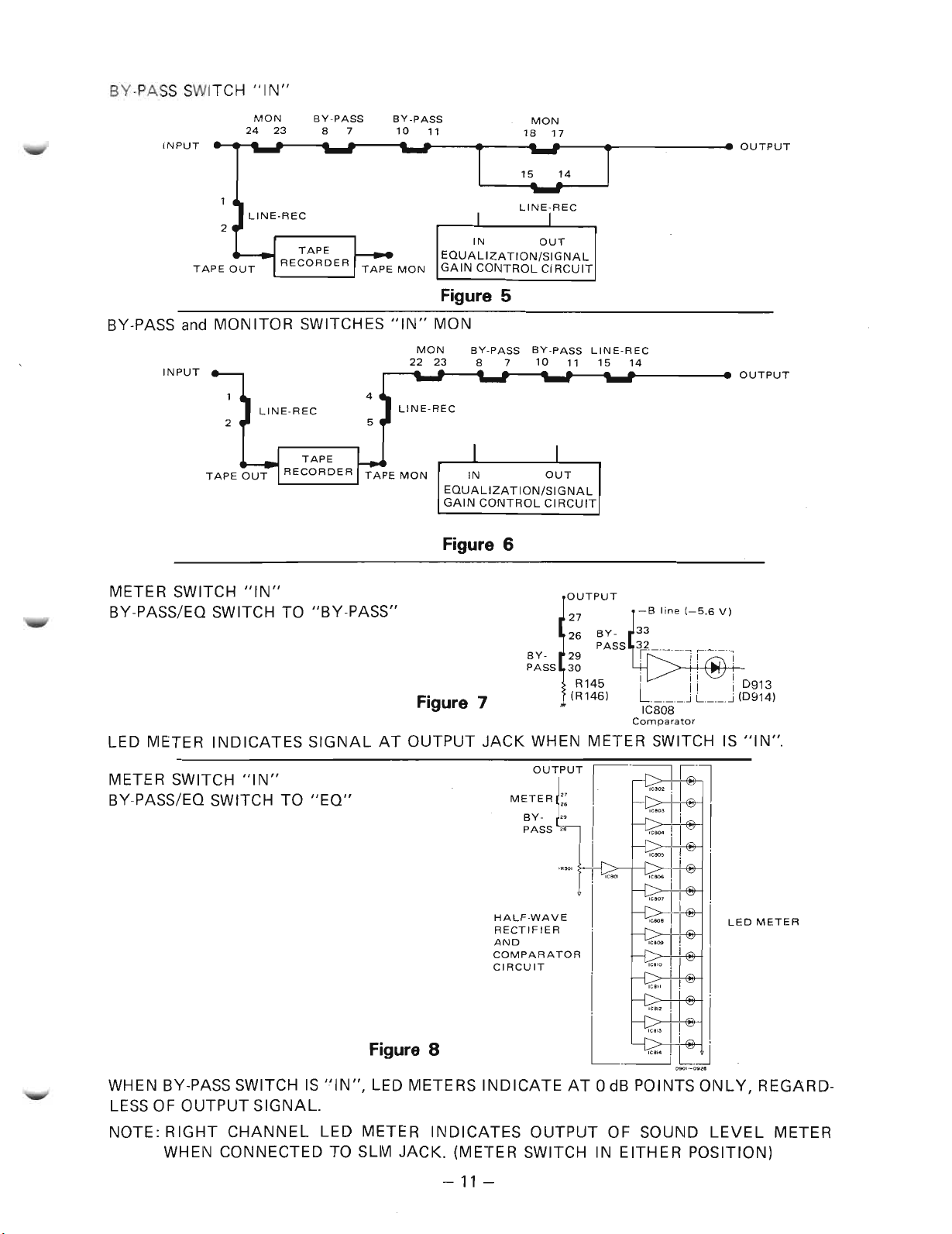
BY-PASS SWITCH "IN"
INPUT
MON
24 23
BY-PASS
8 7
BY-PASS
10 11
EQUALIZATION/SIGNAL
GAIN CONTROL CIRCUIT
Figure 5
BY-PASS and MONITOR SWITCHES "IN" MON
MON BY-PASS BY-PASS L1NE-REC
INPUT OUTPUT
22 23 8 7 10 11 15 14
LINE-REC
EQUALIZATION/SIGNAL
GAIN CONTROL CIRCUIT
MON
18 17
L1NE·REC
IN OUT
IN OUT
Figure 6
METER SWITCH "IN"
BY-PASS/EO SWITCH TO "BY-PASS"
Figure 7
LED METER INDICATES SIGNAL AT OUTPUT JACK WHEN METER SWITCH IS "IN".
METER SWITCH "IN"
BY-PASS/EO SWITCH TO "EO"
METER ::
HALF-WAVE
RECTIFIER
AND
COMPARATOR
CIRCUIT
BY- 29
PASS
OUTPUT
OUTPUT
27
26 BY-
30
R145
(R146)
-B line(-5.6 V)
PASS
Comparator
LED METER
Figure 8
WHEN BY-PASS SWITCH IS "IN", LED METERS INDICATE AT 0 dB POINTS ONLY, REGARD-
LESS OF OUTPUT SIGNAL.
NOTE: RIGHT CHANNEL LED METER INDICATES OUTPUT OF SOUND LEVEL METER
WHEN CONNECTED TO SLM JACK. (METER SWITCH IN EITHER POSITION)
- 11 -
Page 12
METER SWITCH "IN"
BY-PASS/EO SWITCH TO "EO"
INPUT
BY-PASS
~-------------------+~ ,
L..-.-+---!a
EQUALIZER
SIGNAL GAIN
CONTROL CIRCUIT
r--------------------,
I
, I
~ J
SIGNAL GAIN CONTROL
COMPARATOR
>--!,-----i
I
I
,
,
,
,
,
SIGNAL GAIN
LED
01003
(01005)
01002
(01004)
Figure 9
WHEN BY-PASS SWITCH IS "IN" AND METER SWITCH IS "OUT", SIGNAL GAIN CONTROL
LED DOES NOT INDICATE REGARDLESS OF INPUT SIGNAL.
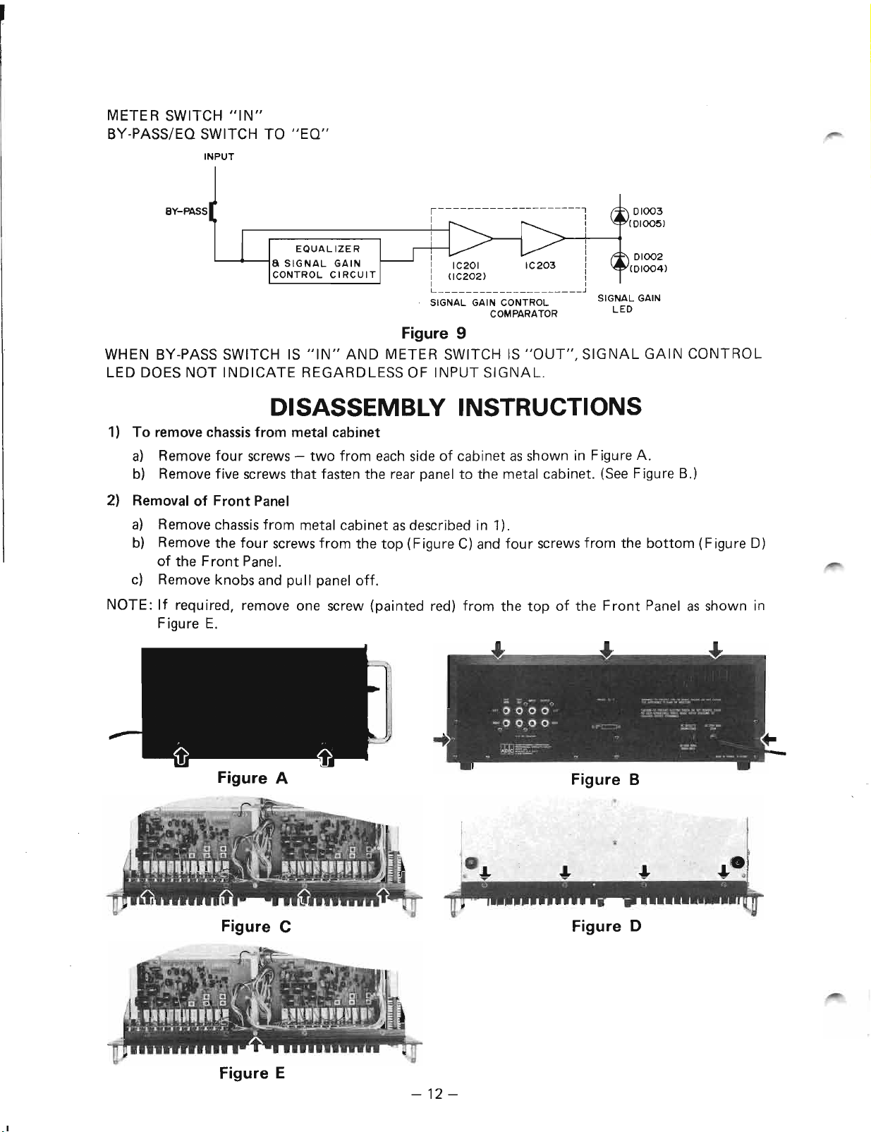
DISASSEMBLY INSTRUCTIONS
1) To remove chassis from metal cabinet
a) Remove four screws - two from each side of cabinet as shown in Figure A.
b) Remove five screws that fasten the rear panel to the metal cabinet. (See Figure B.)
2) Removal of Front Panel
a) Remove chassis from metal cabinet asdescribed in 1).
b) Remove the four screws from the top (Figure C) and four screws from the bottom (Figure D)
of the Front Panel.
c) Remove knobs and pull panel off.
NOTE: If required, remove one screw (painted red) from the top of the Front Panel as shown in
Figure E.
Figure A
Figure C
Figure E
Figure B
Figure D
-12-
Page 13

[L CHANNEL
J
TAP.E MON
TAPE OUT ' FOLLOWER AMP AMP'! FOLLOWER AMP AMP
INPUT
w
I
0
sLM
JACK
f
I:-METER
AMP a
COMPARATOR
L-O-------l RECTIFIER
HALF-WAVE
a AMP
IC801
rr:~QUE-NCY-E-a~Ai~IZATION~AMP---mm-:- :--u-SIGNAL-GAIN-C-ONTROC-AMP---uuu:
I I I I
: EMITTER DIFFERENTIAL FLAT:: EMITTER DIFFERENTIAL FLAT:
, AMP I' AMP ,
TR
VR301
LED
METER
CONTROL
I Ln
o
'"
n
I
TR
'.'~'= __,":'.'n j Lu~: :~_: ___n
SIGNAL GAIN
CONTROL
fSiGNAC
! -~ __
I
L__ _
FRQUENCY EQUALIZER GAIN CONTROL - ~vi~R SUPPLY ~ z
GAIN CoNTROL AMP-
~a~C,OMPARATOR
COMPARATOR
IC 203
SIGNAL GAIN
CONTROL LED
TR :':~:~ - ---
"-
-y
VRIOOI
:L
METER
OUT
T
f-'--t>----,
n_::
"~-:J
I ~
et:
o -
I-
hl
t-
s
I
0..
~ g8~~§
,
,
'
,
:1
I
,
I I
,
, I
, I
, 0702
, -_j
---
/
FREQUENCY SELECTOR
-
--
-
- -
Page 14

ADJUSTMENT PROCEDURES
(1) SIGNAL GAIN CONTROL ADJUSTMENT
EOUIPMENT REOUIREO (See Figure 10)
1. Audio Oscillator
2. AC Voltmeter
3. Calibrator (dB Attenuator)
4. Oscilloscope
NOTE: • Maintain voltage at 120 V AC (UL, C.S.A. and PX) (220/240 V AC for European models).
• Input - INPUT Jack
• Output - OUTPUT Jack
• Set TAPE MONITOR Switch to "OUT".
• Set BY-PASS/EO Switch to "EO".
• Set SIGNAL GAIN Control on Front Panel at center position.
SIGNAL GAIN LED PROCEDURE (See Figure 11)
Step
1.
Adjust Audio Oscillator output for 1 V at 1 KHz as read on AC Voltmeter.
Step 2.
Step 3.
Set Calibrator at 0 dB. Adjust VR 101 (left) for 1 Volt reading on output AC Voltmeter
and VR 102 (right) for 1 Volt reading on output AC Voltmeter.
Adjust VR201 (left) for both LED's (01002 and 01003) to light with equal intensity
and VR202 (right) for both LED's (01004 and 01005) to light with equal intensity.
(2) LED METER CALIBRATION PROCEDURE
Connect LED Meter calibration set-up as shown in Figure 10.
CALIBRATOR: OFF
AC VOLTMETER: 0.3 V Range
AUDIO OSCILLATOR: Frequency - 1 KHz
OUTPUT - 1.5 V min. into ext. 600
INT/EXT LOAD SWITCH (if any) - EXT. (Calibrator box to provide
rl
approximately 600
FREOUENCY EQUALIZER: Frequency Control - Flat position
Center Frequency Selector switch - Center position
METER switch - IN
BY-PASS/EO - EO
TAPE MONITOR - OUT
LlNE/REC - REC
METER CONTROL:
CALIBRATION PROCEDURE (Figure 12)
Step
1.
Set Trimmer Resistors on PCB as indicated below:
VRB01, VRB03, VRB05(L)
VRB02, VRB04, VRB06(R): at 12 o'clock position
2.
Step
Step
Step 4.
Adjust Audio Oscillator output for 1BO mV as read on AC voltmeter.
3.
Set Calibrator at 0 dB. Adjust VRB01 (left) for 12 dB on left LED Meter. And VRB02
(right) for 12 dB on right LED Meter. (All LED's are lit.) (Figure 10A)
Set Calibrator at -1 dB point: check that both 12 dB (left and- right) LED's are turned
(Figure 10B)
Left (VR301) - Max. counterclockwise
Right (VR401) - Max. clockwise
load to generator).
rl
load.
off.
-14 -
Page 15

Step 5. Set Calibrator at -24 dB point.
Adjust VR805 (left) for -12 dB on left LED Meter.
And VR806 (right) for -12 dB on right LED Meter.
Both LED's should be lit. (Figure 10C)
Step 6. Set Calibrator at -25 dB point, check that both -12 dB on left and right LED have
turned off. (Figure 10D)
Step
7.
Set Calibrator at -12 dB point.
Adjust VR803 (left) for 0 dB on left rED Meter.
And VR804 (right) for 0 dB on right LED Meter.
Both LED's should be lit. (Figure 10E)
8.
Step
Set Calibrator at -13 dB point.
Check for both OdB points. Left and right LED haveturned off. (Figure 10F)
Step
9.
RepeatSteps 3 through 8 for optimum performance.
NOTE: Refer to Check Point for each LED Meter below:
CHECK POINT FOR EACH LED METERS
LED Meter point
Calibrator position for
each LED that is lit.
Calibrator position for
each LED that is not lit.
r- --------------------,
I
I
I
CALIBRATION
I
I
(dB ATTENUATORl
I
I
I
I
I
-6 -18
I
-4 20
I
-2
0
(0
AUDIO
OSCILLATOR
o
®
1~lo-
AC VTVM.
,----------------,
i
CALIBRATOR I
I
(dB ATTENUATORl
I I
I 1
i
_;@_10-'2-14-,~,"
-4 -20
-2 -22
~ -24
--------------------~
I
II
I
I
-12 -10 -8
dB
dB
-24 -22 -20 -18 -16 -14
dB
dB dB dB dB dB
-25 -23
dB dB dB dB dB dB
-22
-24
r---
,-----------'
I
I
I I
i
I
I I
I ~
I
I I
0
1
I
L
@--~
"
INPUT OUTPUT
NOTE:
OUTPUT TERMINALS ON SET SHOULD BE CONNECTED TO
CALIBRATOR
(dB ATTENUATORl
_6-@"_10-12_14_16_
-4 -20
0 -24
(-ldB POINT)
-6
dB
dB dB dB
-21
-19 -17 -15 -13 -11
=
iHmm~~
888888888888e@888888888888:
"i
,
-22
_j
Figure 10 B
AC VT.V.M.
L_
_:_O~':·~8.::~~~O~~~
_j
Figure 10A
-15-
(SeeFigure 10 and Figure 10A through 10F.)
-4
-2
-12 -10
+2 +4
0
dB dB
+6 +8 +10 +12
dB dB dB
-8 -6 -4
dB dB dB dB
-2
dB dB dB
-9 -7 -5 -3
SS-3
D
~~i~ii~m~
Figure 10
,-----------1
CALIBRATOR
(dB ATTENUATORl
I
I
I
I
I
I
I
-6-@"_16_
-4 -20
-2 -22
o
L
Figure 10C
1------------'
1
1
(dB ATTENUATORl I
1 I
1
I
_6-@-'~'"
1
-4
1
-2 -22
I
0
I
I
L
Figure 10E
dB dB dB dB
c::=
c::: ~
1
I
I
E24dBi
-24
-20
I
1
I
1
1
I
I
1
I
1
_j
i
I
I
I
I
1
-10 -12 -14
,s
(-24dB POINT)
CALIBRATOR
-10ElE!l_14
I
(-12 dB POINT)
1
J
dB dB dB
OSCILLOSCOPE
r-r-r--
f-o
ACV.T.VM
I~I
r'
IOKO
LOAD
7fr
10 Kn
------
r
CALIBRATOR
I
I
(dB ATTENUATORl
I
I
I
I
I
1
I
I
I I
I
L
,---------,--,
I
I
I I
I _s@_,O
I
(-25dB POINT)
Figure 100
CALIBRATOR
(dB ATTENUATORl
-6 -IS
1
-4 -20
I
-2 -22
I
0
I
L__
~-~d~~~~ __
Figure 10 F
dB dB
-1
e
LOAD.
------l
-t~_16
-24
0
I
I
I
I
I
I
I
I
I
I
__J
I
I
i
1
I
I
1
I
J
Page 16

AMP P.C.B.
POWER SUPP LV
VR802
&
METER P
.C. B.
~
I
I
I
I
0
VA202
0
~
VR102
0
~
VA201
~
~
VRIOI
~DDOOOO
~
VR801
VR803
~ ®
~OOOOOO~O
~ ~
VR806 VR804
Figure 11 Figure 12
CALIBRATOR SCHEMATIC
RI
AUDIO
GENERATOR
510.Cl
R2
17.Cl
+12dB
AC
VOLTMETER
NOTE:
All resistors are
%W or 'hW, carbon.
±
5% or better,
R3
13.Cl
R4
Ion
R5
9.1.Cl
R6
S.S.Cl
R7
5.6.Cl
RS
4.3.Cl
R9
3.3n
RIO
2.7n
RII
2.2n
RI2
1.7n
RI3
1.3.Cl
RI4
5.1.Cl
L
OUTPUT TO
SS 3
- 16-
R
Page 17

TROUBLESHOOTI NG
SYMPTOM
1) No output
2) Power indicator LED does not
light.
3) Power indicator lights but no
output.
4) No output with test signal
appl ied to the input terminals.
5) "TAPE OUT" inoperative
6) "I NPUT" inoperative
7) "OUTPUT" inoperative
8) "TAPE MONITOR" inoperative
9) Frequency control 26/32/39 Hz
has no effect.
10) Frequency control 47/56/68 Hz
has no effect.
11) Frequency control 84/100/120
Hz has no effect.
12) Frequency control 150/180/215 1) Faulty VR504/604
Hz has no effect.
1) Faulty AC power cord
*Replace the cord.
2) Defective power switch
"Replace the switch.
3) Broken wire in the power transformer (Tl00l)
*Replace the transformer.
4) Check Fuse, European and PX only.
1) Defective LED Dl00l
*Replace the LED.
2) Open in the power transformer secondary winding
*Replace the transformer.
3) Check Fuse, European and PX only.
1) Defective diode D702 and/or D703
"Replace the diode{s).
2) Defective transistor TR701 and/or TR702
*Replace the transistor{s).
1) Defective transistor TR 101-116
*Replace the transistor{s).
2) Defective resistor or capacitor of Main Amp stage
*Replace the defective part{s).
1) Poor contact in "TAPE OUT" input jacks
*Repair or replace the jacks.
2) Faulty TAPE MONitor switch
*Repair or replace the switch.
1) Poor contact in "I NPUT" input jacks
*Repair or replace the jacks.
1) Poor contact in "OUTPUT" output jacks
"Repair or replace the jacks.
1) Poor contact in "TAPE MONitor" input jack
*Repair or replace the jack.
2) Faulty "TAPE MONitor" switch
*Repair or replace the switch.
1) Faulty VR501/601
*Repair or replace.
2) Defective R301 /401, 335/435, 336/436 or L301/401
*Replace the defective
1) Faulty VR502/602
*Repair or replace.
2) Defective R302/402, 303/403, 304/404, 337/437,338/438 or L302/402
"Replace,
1) Faulty VR503/603
*Repair or replace.
2) Defective R305/405, 306/406, 307/407, 339/439, 340/440 or L303/403
*Replace.
*Repair or replace.
2) Defective R308/408, 309/409, 310/410, 341/441, 342/442 or L304/404
*Replace.
CAUSE/REMEDY
0
parts.
-17-
Page 18

SYMPTOM
13) Frequency control 260/320/390 1) Faulty VR505/605
Hz has no effect. "Repair or replace.
2) Defective R311/411, 312/412, 313/413, 343/443, 344/444 or L305/405
"Replace.
14) Frequency control 470/560/680 1) Faulty VR505/605
Hz has no effect. "Repair or replace.
2) Defective R314/414, 315/415, 316/416, 345/445, 346/446 or L306/406
"Replace.
15) Frequency control 840/1 K/l.2 K 1) Faulty VR507/607
Hz has no effect. "Repair or replace.
2) Defective R317/417, 318/418/319/419, 347/447, 348/448 or L307/407
"Replace.
16) Frequency control 1.5 K/l.8 K/ 1) Faulty VR508/608
2.15 K Hz has no effect.
17) Frequency control 2.6 K/3.2 K/
3.9K Hz has no effect.
18) Frequency control 4.7 K/5.6 K/
6.8K Hz has no effect. "Repair or replace.
19) Frequency control 8.4 K/l 0 K/
12 K Hz has no effect. "Repair or replace.
20) Frequency control 15 K/18 K/
21.5 K Hz has no effect. "Repair or replace.
21) All controls have no effect.
22) LED Meter does not light up.
23) SIGNAL GAIN Control indicator 1) Defective TR 109-116
(LED) does not light up.
24) Popping Noise Protector does
not operate.
"Repair or replace.
2) Defective R320/420, 321/421,322/422,349/449,350/450 or L308/408
"Replace.
1) Faulty VR510/610
"Repair or replace.
2) Defective R323/423, 324/424, 325/425, 351/451,352/452 or L309/409
"Replace.
1) Faulty VR511/611
2) Defective R326/426, 327/427,328/428,353/453,354/454 or L310/41 0
"Replace.
1) Faulty VR511/611
2) Defective R329/429, 330/430, 331/431, 355/455, 356/456 or L311 /411
"Replace.
1) Faulty VR512/612
2) Defective R332/432, 333/433, 334/434, 357/457, 358/458 or L312/412
"Replace.
1) Defective Rlll/112 or Rl15/116
"Replace.
2) Defective Transistor TR 103-1 06
*Replace.
1) Defective IC801
"Replace.
2) Defective IC802-814
*Replace.
3) Defective LED Meter D901-926
"Replace.
2) Defective IC201-203
3) Defective LED Dl 002-1 005
4) Defective Diode D207-210
1) Defective TR201-203
2) Defective D205 or D206
3) Defective Reed Relay
CAUSE/REMEDY
j
"Replace.
"Replace.
"Replace.
"Replace.
*Replace.
"Replace.
*Repair or replace.
- 18-
Page 19

AMP P.C.B.(TOP
&
BOTTOM VIEWS)
TOP VIEW
t
I
BOTTOM VIEW
-19-
Page 20

POWER SUPPLY
&
METER
p.e.B.
{TOP
&
BOTTOM VIEWS}
TOP VIEW
BOTTOM VIEW
- 20-
Page 21

SWITCH (L) P.C.B. (TOP
TOP VIEW
&
BOTTOM VIEWS) .
BOTTOM VIEW
- 21 -
Page 22

SWITCH (R) P.C.B. (TOP & BOTTOM VIEWS)
TOP VIEW
BOTTOM VIEW
- 22-
Page 23

SLIDE VOLUME (L)
=.c.e.
TOP VIEW
(TOP
&
BOTTOM VIEWS)
BOTTOM VIEW
- 23-
....-
Page 24

SLIDE VOLUME (R)
=.c.e.
TOP VIEW
(TOP
&
BOTTOM VIEWS)
BOTTOM VIEW
- 24-
Page 25

ELECTRICAL PARTS LIST
NOTE: 1. ,. marks value changed during the course of production.
2. Serial number is indicated on the rear panel of the unit.
REF. NO.
CAPACITORS
Cl01/102
Cl03/104
C105/1 06
C107/108
C109/110
C111/112
C113/114
C 115/116
C117/118
C119/120
C121/122
C123/124
C125/126
C201/202
C2031204
C205/206
C207/208
C209/210
C211
C212/213
DESCRIPTION
Electrolytic
Tantalum
Ceramic
Ceramic
Ceramic
Electrolytic
Electrolytic
Tantalum
Ceramic
Electrolytic
Ceramic
Ceramic
Electrolytic 22,uF
Mylar 0.1 ,uF 50V
Mylar 0.1 ,uF
Electrolytic
Electrolytic
Ceramic
Electrolytic 100,uF
Ceramic
47 ,uF
2.2,u
100 pF 50V
10 pF
33 pF 50V
10,u
47,uF 50V 31-25-1061
2.2 ,uF
100 pF 50V
47,uF 35 V 31-25-1351
18 pF
47 pF
4.7 ,uF
4.7 ,uF 25 V 31-25-1353
150 pF 50V
0.047,uF 50V 31-25-1366
25 V
35 V 31-25-1059
F
50V ±5 %
35 V 31-25-1207
F
35 V 31-25-1059
50V ±5% 31-25-1364
50V ±5% 31-25-1365
35 V 31-25-1352
50V
25 V
16 V 31-25-1354
±5%
±5 %
±5 %
±5 %
±5%
±5%
BSR/ADC MFR'S
PART NO. PART NO.
31-25-1354
31-25-1028
31-25-1026
31-25-1068
31-25-1028
31-25-1099
31-25-1099
31-25-1353
31-25-1368
C301/401
C302/402
C303/403
C304/404
C305/405
C306/406
C307/407
C308/408
C309/409
C310/410
C311/411
C312/412
C313/413
*C314/414
*C314/414
C315/415
C316/416
C317/417
C318/418
C319/419
C320/420
C321/421
C322/422
Not used
Tantalum
Tantalum
Mylar 0.22,uF 50V
Tantalum 3.3 ,uF
Mylar 0.22,uF
Tantalum
Tantalum
Tantalum
Mylar
Tantalum
Mylar
Tantalum
Mylar 0.15,uF
(Use Serial No.1 through 1000)
Mylar
(Use after Serial No. 1001)
Tantalum
Mylar
Tantalum
Mylar
Tantalum
Tantalum
Tantalum
Mylar
4.7 ,uF
1 ,uF 35 V
2.2,uF
0.47,uF
2.2,u
0.47,uF 50V
1.5 ,uF 35 V
0.27,uF 50V
1 ,uF
0.068,uF
1.5 ,uF 35 V
0.15,u
1 ,uF
0.15,u
0.68,uF 35 V
1 ,uF 35 V
0.68,uF
0.047,uF
35 V
35 V
50V
35 V ±10 %
35 V
35 V
F
35 V ±10 %
50V
50V ±3 % 31-25-1380
50V ±3 %
F
35 V ±10 %
50V
F
35 V
50V
±10%
±10 %
±3 %
±10 %
±3 %
±10 %
±10 %
±3 %
±10%
±3 %
±3 %
±10 %
±3 %
±3 %
±3 %
±3 %
±3 %
31-25-1054
31-25-1079
31-25-1326
31-25-1077
31-25-1366
31-25-1202
31-25-1080
31-25-1202
31-25-1327
31-25-1204
31-25-1328
31-25-1079
31-25-1330
31-25-1078
31-25-1330
31-25-1079
31-25-1330
31-25-1201
31-25-1079
31-25-1201
31-25-1331
- 25-
Page 26

REF. NO. DESCR IPTION
BSR/ADC
PART NO.
MFR'S
PART NO.
C323/423
C324/424
C325/425 Tantalum
C326/426
C327/427
C328/428
C329/429
C330/430
C331/431 Not used
C332/432
C333/433
C334/434
C335/435 Mylar
C336/436 Mylar
C337/437
*C338/438 Mylar
*C338/438
C339/439
C340/440 Mylar
C341/441 Mylar
C342/442 Mylar
*C343/443 Mylar
*C343/443
C344/444 Mylar
C345/445 Mylar
C346/446 Mylar
C347/447
C348/448 Mylar
C349/449 Mylar
C350/450 Mylar
C351/451 Mylar
C352/452 Mylar
C353/453 Mylar
C354/454 Mylar
C355/455 Mylar
C356/456 Mylar
C357/457
C358/458 Mylar
C359/459 Mylar
C360/460
C361/461 Mylar
C362/462
C363/463
C364/464
Tantalum
Mylar
Mylar
Mylar
Mylar
Mylar
Mylar
Mylar
Mylar
Mylar
Mylar
Mylar
Mylar
Mylar
Polystyrene
Mylar
Mylar
Mylar
Mylar
Mylar
0.47/lF
0.15/lF
0.47/lF
0.39/lF
0.047/lF
0.22/lF
0.27/lF
0.22/lF
0.15/lF
0.015/lF
0.15/lF
0.018/lF 50V
0.1 /IF
0.082/lF
0.0082/lF 50V
(Use for Serial No.1 through 2000)
0.012/lF 50V
(Use after Serial No. 2001)
0.082/lF 50V
0.068/lF
0.0082/lF 50V
0.039/lF
0.0033/lF
(Use for Serial No.1 through 5000)
0.0068/lF
(Use after Serial No. 5001)
0.056/lF
0.0082/lF
0.033/lF
820pF 50V
0.027/lF 50V
0.0039/lF 50V
0.027/lF 50V
0.022/lF
0.0047/lF 50V ±3
0.01 /IF
0.0018/lF 50V
0.015 /IF
0.012 /IF 50V
0.0082/lF 50V
0.0012/lF
0.0056/lF
0.0047/lF 50V
0.068/lF 50V ±3
0.039/lF 50V ±3
0.0082/lF
0.001 /IF 50V
35 V
50V
35 V ±10
50V
50V
50V
50V
50V
50V
50V
50V
50V
50V
50V
50V
50V
50V
50 V
50V
50 V
50V
50V ±3
50V ±3
50V ±3
50 V
50V
±10
±3
±3
±3
±3
±3
±3
±3
±3
±3
±3
±3
±3
±3
±3
±3
±3
±3
±5
±3
±3
±3
±3
±3
±3
±3
±3
±3
±3
±3
±3
±3
±3
±3
±3
±3
%
%
%
%
%
%
%
%
%
%
%
%
%
%
%
%
%
%
%
%
%
%
%
%
%
%
%
%
%
%
%
%
%
%
%
%
%
%
%
%
%
%
%
31-25-1080
31-25-1330
31-25-1080
31-25-1332
31-25-1331
31-25-1333
31-25-1328
31-25-1333
31-25-1330
31-25-1334
31-25-1330
31-25-1376
31-25-1377
31-25-1378
31-25-1379
31-25-1392
31-25-1378
31-25-1380
31-25-1379
31-25-1382
31-25-1383
31-25-1397
31-25-1381
31-25-1379
31-25-1384
31-25-1396
31-25-1385
31-25-1386
31-25-1385
31-25-1387
31-25-1388
31-25-1389
31-25-1390
31-25-1391
31-25-1392
31-25-1379
31-25-1393
31-25-1394
31-25-1388
31-25-1380
31-25-1382
31-25-1379
31-25-1395
C701/702 Electrolytic
C703 Electrolytic
C704
C705
Electrolytic
Electrolytic 47/lF
220/lF 50V 31-25-1071
47/lF 35 V
330/lF 80V 31-25-1356
10 V
- 26-
31-25-1351
31-25-1357
Page 27

REF. NO.
DESCRIPTION
BSR/ADC MFR'S
PART NO. PART NO.
C706
C707
C708
C709/710
C711/712
C713/714
C715
C716
C801/802
C803/804
C805/806
C807/808
Cl00l
Cl00l
Cl00l
Cl00l
Cl 002/1 003
Cl004
Electrolytic
Electrolytic
Electrolytic
Electrolytic
Electrolytic
Electrolytic
Electrolytic
Ceramic
Tantalum
Ceramic
Ceramic
Electrolytic
Ceramic for Line Pass
0.01 ,uF
Ceramic for Line Pass
0.01 ,uF
Ceramic for Line Pass
0.01 ,uF
Ceramic for Line Pass
0.01 J.lF
Ceramic
Ceramic for Line Pass
0.01 ,uF
330,uF
100,uF
47,uF
100,u
100,u
470,uF
4.7 ,uF
0.047,uF
4.7 ,uF 35 V
30 pF 50 V
330 pF
10,u
125 V UK or LB type (U.S.A.) 31-25-1064
125 V MY type (Canadian) 31-25-1025 P-220044
250 V X type (European) 31-25-1002 P-220022
250 V X type (PX) 31-25-1002 P-220022
0.01 ,uF
250 V X type (European) 31-25-1002 P-220022
16 V 31-25-1358
16 V 31-25-1359
16 V 31-25-1360
35 V 31-25-1355
F
35 V
F
35 V 31-25-1359
50V
50V
±5%
50V
25 V 31-25-1208
F
50V 31-25-1369
±5 %
31-25-1355
31-25-1363
31-25-1366
31-25-1054
31-25-1027
31-25-1367
DIODES
0201/202
0203/204
0205/206
0207/208
0209/210
0701
0702/703
0704/705
0706/707
0708
0709
0710
0801/802
0803/804
0805/806
0807/808
0809/810
0811/812
0813/814
0815/816
0817/818
0819/820
0821/822
0823/824
Si Diode
Si Diode
Si Diode
Si Diode
Si Diode
Bridge Diode
Si Diode
Zener Diode
Si Diode
Zener Diode
Si Diode
Zener Diode
Si Diode
Si Diode
Si Diode
Si Diode
Si Diode
Si Diode
Si Diode
Si Diode
Si Diode
Si Diode
Si Diode
Si Diode
ITT-73N 31-53-1057
ITT-73N 31-53-1057
10E-lorSR-1K-2
ITT-73N 31-53-1057
ITT-73N
SVB-l0-200
10E-lorSR-1K-2 31-53-1053
WZ-220
10E-l or SR-l K-2 31-53-1053
WZ-056 or HZ-6B 1 31-53-1064
10E-lorSR-1K-2 31-53-1053
WZ-056 or HZ-6B 1 31-53-1064
ITT-73N 31-53-1057
ITT-73N 31-53-1057
ITT-73N 31-53-1057
ITT-73N
ITT-73N
ITT-73N 31-53-1057
ITT-73N 31-53-1057
ITT-73N
ITT-73N 31-53-1057
ITT-73N 31-53-1057
ITT-73N 31-53-1057
ITT-73N 31-53-1057
31-53-1053
31-53-1057
31-53-1 063 .~
31-53-1070
31-53-1057
31-53-1057
31-53-1057
- 27-
Page 28

REF. NO.
DESCRIPTION
BSR/ADC
PART NO.
MFR'S
PART NO.
I~
D825/826
D827/828
D829/830
Si Diode
Si Diode ITT-73N
Si Diode ITT-73N
ITT-73N 31-53-1057
FUSES
Midget Fuse 160 mAT/250 V
Midget Fuse 315 mAT/250 V
Fuse
1 A/250 V
INTEGRATED CIRCUITS
IC201 IC NJM4558DM
IC202 IC
IC203 IC NJM4558DM
IC801
IC802
IC803
IC804
IC805 IC
IC806 IC
IC807 IC
IC808 Ie
IC809 IC
IC810 IC NJM4558DM
IC811
IC812 IC
IC813 IC
IC814
IC
IC NJM4558DM
IC
IC NJM4558DM 31-54-1453
IC NJM4558DM 31-54-1453
IC
NJM4558DM
RC4709
NJM4558DM
NJM4558DM 31-54-1453
NJM4558DM
NJM4558DM
NJM4558DM
NJM4558DM
NJM4558DM 31-54-1453
NJM4558DM 31-54-1453
NJM4558DM
31-53-1057
31-53-1057
(European) 31-22-1407
(European)
(PX)
31-22-1415
31-22-1416
31-54-1453
31-54-1453
31-54-1453
31-54-1451
31-54-1453
31-54-1453
31-54-1453
31-54-1453
31-54-1453
31-54-1453
31-54-1453
31-54-1453
P-250105
P-250084
P-250059
INDUCTORS
L301/401 Inductor 6H ±3 % 31-36-1851
L302/402 Inductor
L303/403 Inductor
L304/404 Inductor
L305/405
L306/406 Inductor
L307/407 Inductor
L308/408 Inductor
L309/409 Inductor
L310/410
L311/411 Inductor
L312/412
Inductor
Inductor
Inductor
3.8 H ±3 % 31-36-1852 P-370048S
2.05 H ±3 % 31-36-1853
1 H ±3 %
0.6 H
0.36 H ±3 % 31-36-1856
0.21 H ±3 %
0.12 H ±3 % 31-36-1858 P-370023S
0.06 H
0.037 H ±3 % 31-36-1860
0.021 H
0.012 H ±3 %
±3 %
±3%
±3 %
31-36-1854
31-36-1855
31-36-1857
31-36-1859
31-36-1861 P-370026S
31-36-1862 P-370027S
LED's
D901-D926
D1001 LED SLP-144B (red)
D 1002/D 1003 LED GL-9PR3 (red)
D 1004/D 1005 LED GL-9PR3 (red)
LED Meter (red)
31-53-1069
Power Indicator 31-53-1068
Signal Level Indicator 31-53-1071
Signal Level Indicator
- 28-
31-53-1071
P-370044S
P-370045S
P-370051S
P-370052S
P-370062S
P-370054S
P-370024S
P-370025S
Page 29

REF. NO.
JUMPER WIRE
(AMP Board)
J1/3/10/11
J2/4/5/12-
21
J7/8/9
J6
(SWITCH L
J 1/2/3
(POWER SUPPLY
J1-8
J9
J 10
Jumper Wire
Jumper Wire
Jumper Wire
Jumper Wire
&
R Board)
I
Jumper Wire
Jumper Wire
Jumper Wire
Jumper Wire
RELAY
DESCRIPTION
&
METER Board)
BSR/ADC MFR'S
PART NO. PART NO.
7.5 mm P-320126
10 mm
12.5 mm P-320128
17.5 mm P-320130
10 mm
10mm
15 mm P-320129
12.5 mm
P-320127
P-320127
P-320127
P-320128
Reed Relay
RESISTORS
R 101/102
R103/104
R105/106
R107/1 08 Carbon
R109/110
R111/112
R113/114
R115/116
R117/118
R119/120
R121/122
R123/124
R125/126
R127/128
R129/130
R131/132
R133/134
R135/136 Carbon
R137/138
R139/140
R141/142 Carbon
R 143/144
R145/146 Carbon
R147/148
Carbon
Carbon
Carbon
Carbon
Carbon
Carbon
Carbon
Carbon
Metal Oxide
Carbon
Carbon
Carbon
Carbon
Carbon
Carbon
Carbon
Carbon
Metal Oxide
Carbon
Carbon
L23M 12 V 31-16-1036 P-290022
%WPZ 1 K~ J
% WPZ
%WPZ 220 K~ J
%WPZ
%WPZ
%WPZ
%WPZ
%WPZ 22 K~ J
%WPZ 3.3 K~ J
1W
%WPZ 120 K~ J
%WPZ 1 K~ J
% WPZ
%WPZ 270 K~ J
%WPZ 3.3 K~ J
%WPZ
% WPZ
%WPZ
%W PZ 15 K~ J
1W 2.2 K~ J
%WPZ 3.3 K~ J
%WPZ 1 K~ J
%WPZ 47 K~ J
%WPZ 470 K~ J
120 K~ J 31-23-1001-124
270 K~ J
3.3 K~ J 31-23-1001-332
3.3 K~ J
3.3 K~ J 31-23-1001-332
2.2 K~ J
47 K~ J
5.6 K~ J 31-23-1001-562
22 K~ J
5.6 K~ J
31-23- 1001- 102
31-23-1001-224
31-23-1001-274
31-23-1002-332
31-23-1001-223
31-23-1001-332
31-23-1003-222
31-23-1001-124
31-23-1001-1 02
31-23-1001-473
31-23-1001-274
31-23-1001-332
31-23-1001-223
31-23-1001-562
31-23-1001-153
31-23-1003-222
31-23-1002-332
31-23- 1001- 102
31-23-1001-473
31-23-1001-474
R201/202
R203/204
R205/206
R207/208
Carbon
Carbon
Carbon
Carbon
%WPZ 10 K~ J
%WPZ
%WPZ 4.7 K~ J
%WPZ
4.7 K~ J
47 ~ J
- 29-
31-23-1001-103
31-23-1001-472
31-23-1001-472
31-23-1001-470
Page 30

REF. NO.
DESCRIPTION
BSR/ADC
PART NO.
MFR'S
PART NO.
R209/21 0 Carbon
R211/212 Carbon
R213/214 Carbon
R215/216
R217/218
Carbon
Carbon
R219/220 Carbon
R221/222
R223/224
R225/226
R227/228
R229/230
R231/232
R233/234
R2351236
Carbon
Carbon
Carbon
Carbon
Carbon
Carbon
Carbon
Carbon
R237 Carbon
R238
Carbon
R239 Carbon
R240/241 Carbon
R242 Carbon
R243/244 Carbon
R245/246 Carbon
R247/248 Carbon
R249/250 Carbon
R251/252 Carbon
%WPZ
%WPZ
%WPZ
%WPZ
%WPZ
%WPZ
%WPZ
%WPZ
%WPZ
%WPZ
%WPZ
% W PZ
% WPZ
%WPZ
%WPZ
%WPZ
% VVPZ
%W PZ
%W PZ
%W PZ
%W PZ
%W PZ
% WPZ
% W PZ
3.3 Kn J
10 Kn J
22 Kn J
22 Kn J
31-23-1001-332
31-23- 1001- 103
31-23-1001-223
31-23-1001-223
1 Kn J 31- 23- 1001-1 02
91 Kn J
31-23-1001-913
10 Kn J 31-23-1001-103
2.2 Kn J
91 Kn J
2.2 Kn J
2.2 Mn J
2.2 Kn J
10 Kn J
100 n J
33 Kn J
15 Kn J
560 Kn J
10 Kn J
100 n J
2.2 Kn J
390 n J
390 n J
2.2 Kn J
10 Kn J
31-23-1001-222
31-23-1001-913
31-23-1001-222
31-23-1001-225
31-23-1001-222
31-23-1001-103
31-23-1001-101
31-23-1001-333
31-23-1001-153
31-23-1001-564
31-23- 1001-1 03
31-23-1001-1 01
31-23-1001-222
31-23-1001-391
31-23-1001-391
31-23-1001-222
31-23-1001-103
R301/401 Carbon
R302/402
R303/403
R304/404
R305/405
Carbon
Carbon
Carbon
Carbon
R306/406 Carbon
R307/407
Carbon
R308/408 Carbon
R309/409
Carbon
R310/410 Carbon
R311/411 Carbon
R312/412 Carbon
R313/413 Carbon
R314/414 Carbon
R315/415 Carbon
R316/416 Carbon
R317/417 Carbon
R318/418 Carbon
R319/419 Carbon
R320/420 Carbon
R321/421
Carbon
R322/422 Carbon
R323/423 Carbon
R324/424 Carbon
R325/425 Carbon
R326/426
Carbon
R327/427 Carbon
%W PZ
% WPZ
%WPZ
% WPZ
%WPZ
%WPZ
%WPZ
% WPZ
%W PZ
% WPZ
%W PZ
% WPZ
%WPZ
% WPZ
%W PZ
% W PZ
% WPZ
%W PZ
%WPZ
%W PZ
%WPZ
%WPZ
%WPZ
% WPZ
%WPZ
%WPZ
%WPZ
330 n J
220 n J
180 n J
150 n J
270 n J
31-23- 1001-331
31-23-1001-221
31-23-1001-181
31-23-1001-151
31-23-1001-271
240 n J 31-23-1001-241
200 n J
240 n J
200 n J
220 n J
240 n J
240 n J
31-23-1001-201
31-23-1001-241
31-23-1001-201
31-23-1001-221
31-23-1001-241
31-23-1001-241
240 n J 31-23-1001-241
330 n J
330 n J
300 n J
390 n J
390 n J
360 n J
300 n J
330 n J
330 n J
360 n J
360 n J
360 n J
430 n J
470 n J
31-23-1001-331
31-23-1001-331
31-23- 1001-301
31-23-1001-391
31-23-1001-391
31-23-1001-361
31-23-1001-301
31-23-1001-331
31-23-1001-331
31-23-1001-361
31-23-1001-361
31-23-1001-361
31-23- 1001-431
31-23- 1001-471
- 30-
Page 31

REF. NO.
DESCRIPTION
BSR/ADC
PART NO.
MFR'S
PART NO.
R328/428
R329/429
R330/430
R331/431
R332/432
R333/433
R334/434
R335/435
R336/436
R337/437
R338/438
R339/439
R340/440
R341/441
R342/442
R343/443
R344/444
R345/445
R346/446
R347/447
R348/448
R349/449
R350/450
R351/451
R352/452
R353/453
R354/454
R355/455
R356/456
R357/457
R358/458
Carbon
Carbon
Carbon
Carbon
Carbon
Carbon
Carbon
Carbon
Carbon
Carbon
Carbon
Carbon
Carbon
Carbon
Carbon
Carbon
Carbon
Carbon
Carbon
Carbon
Carbon
Carbon
Carbon
Carbon
Carbon
Carbon
Carbon
Carbon
Carbon
Carbon
Carbon
%W PZ
%WPZ
470 n J 31-23-1001-471
510n J
31-23-1001-511
% WPZ 510n J 31-23-1001-531
% W PZ 510nJ 31-23-1001-531
%WPZ
% WPZ
560 n J
560 n J
31-23-1001-561
31-23-1001-561
% W PZ 560 n J 31-23-1001-561
%W PZ 470 Kn J
%WPZ 470 Kn J
%WPZ 470 Kn J
31-23-1001-474
31-23-1001-474
31-23-1001-474
%WPZ 470 Kn J 31-23-1001-474
%WPZ 470 Kn J
%W PZ
%WPZ
470 Kn J
470 Kn J
%WPZ 470 Kn J
31-23-1001-474
31-23-1001-474
31-23- 1001 -474
31-23- 1001-474
%WPZ 470 Kn J 31-23-1001-474
% WPZ 470 Kn J
31-23-1001-474
%WPZ 470 Kn J 31-23-1001-474
%W PZ 470 Kn J 31-23-1001-474
% W PZ 470 Kn J 31-23-1001-474
% W PZ
%W PZ
%W PZ
% WPZ
% WPZ
% WPZ
%WPZ
%WPZ
%WPZ
%WPZ
470 Kn J
470KnJ
470 Kn J
470 Kn J 31-23-1001-474
470 Kn J
470 Kn J 31-23-1001-474
470 Kn J
470 Kn J
470 Kn J
470 Kn J
%WPZ 470 Kn J
31-23-1001-474
31-23-1001-474
31-23-1001-474
31-23-1001-474
31-23-1001-474
31-23-1001-474
31-23-1001-474
31-23-1001-474
31-23-1001-474
R701
R702
R703
R704
R705
R706
R707
R708
R709
R710
R711
R712/713
R714/715
R716/717
R718
R719
R801/802
R803/804
R805/806
Metal Oxide
Carbon
Carbon
Carbon
Carbon
Carbon
Carbon
Carbon
Carbon
Carbon
Carbon
Carbon
Carbon
Metal Oxide
Carbon
Carbon
Carbon
Carbon
Carbon
2W
%WPZ
%WPZ
%WPZ
%WPZ
22 n J 31-23-1004-220
3.3 Kn J
31-23-1001-332
8.2 Kn J 31-23-1001-822
3.3 Kn J 31-23-1001-332
470 Kn J
31-23-1001-474
%WPZ 22 Kn J 31-23-1001-223
%W PZ 1 Kn J 31-23- 1001- 102
%WPZ 33 Kn J
31-23-1001-333
% W PZ 22 Kn J 31-23-1001-223
% W PZ
% W PZ 22 Kn J
%W PZ
% W PZ
2W
% WPZ
% W PZ 3.3 Kn J
1 Kn J
31-23- 1001- 102
31-23-1001-223
1 Kn J
1 Kn J
31-23- 100 1-102
31-23-1001-102
56 n J 31-23-1004-560
47 Kn J
31-23-1001-473
31-23-1001-332
% WPZ 100 Kn J 31-23-1001-104
% W PZ
100 Kn J
31-23- 1001-1 04
% W PZ 22 Kn J 31-23-1001-223
-31-
Page 32

REF. NO. DESCRIPTION
BSR/ADC
PART NO.
MFR'S
PART NO.
R807/808
R809/81 0 Carbon
R811/812
R813/814 Carbon
R815/816 Carbon
R817/818
R819/820 Carbon
R821/822
R823/824 Carbon
R825/826 Carbon
R827/828 Carbon
R829/830
R831/832 Carbon
R833/834 Carbon
R835/836 Carbon
R837/838 Carbon
R839/840
R841/842 Carbon
R843/844 Carbon
R845/846 Carbon
R847/848 Carbon
R849/850 Carbon
R851/852 Carbon
R853/854 Carbon
R855/856 Carbon
R857/858 Carbon
R859/860 Carbon
R861/862 Carbon
R863/864 Carbon
R865/866 Carbon
R867/868
R869/870
R871/872 Carbon
R873/874 Carbon
R875/876 Carbon
R877/87S
R879/880 Carbon
R881/882 Carbon
R883/884 Carbon
R885/886 Carbon
R887/888 Carbon
R889/890 Carbon
R891/892 Carbon
R893/894 Carbon
R895/896 Carbon
R897/898 Carbon
R899/900 Carbon
R901/902
R903/904 Carbon
R905/906 Carbon
R907/908 Carbon
R909/910 Carbon
Carbon
Carbon
Carbon
Carbon
Carbon
Carbon
Carbon
Carbon
Carbon
Carbon
% W PZ
% W PZ
% WPZ
% WPZ
% W PZ
% WPZ
%W PZ
%WPZ
% W PZ
% WPZ
% W PZ
%WPZ
%WPZ
% WPZ
%WPZ
% W PZ
%W PZ
% WPZ
% WPZ
% WPZ
%WPZ
%WPZ
%W PZ
%W PZ
%W PZ
% W PZ
%W PZ
%W PZ
%W PZ
%W PZ
% W PZ
% W PZ
% W PZ
% W PZ
% W PZ
% W PZ
% W PZ
% W PZ
% W PZ
% WPZ
% WPZ
%WPZ
%WPZ
% W PZ
% W PZ
% WPZ
% WPZ
% W PZ
% W PZ
% W PZ
% W PZ
% W PZ
1.5 KSl J
10 KSl J
10 KSl J 31- 23- 1001-1 03
1.8 KSl J
10 KSl J
1.5 KSl J
10 KSl J
1.1 KSl J
10 KSl J
910 Sl
10 KSl J
620 Sl
10 KSl J
560 Sl
10 KSl J
10 KSl J 31-23-1001-103
300 Sl
10 KSl J 31-23-1001-103
220Sl
10 KSl J
150 Sl
10 KSl J 31-23-1001-103
130 Sl
10 KSl J 31-23-1001-103
10 KSl J 31- 23-1 001- 103
2.2MSl J 31-23-1001-225
2.2MSl J 31-23-1001-225
2.2MSl J 31-23-1001-225
2.2MQ J
2.2 MSl J
2.2MSl J 31-23-1001-225
2.2 MSl J
2.2 MSl J
2.2 MSl J 31-23-1001-225
2.2 MSl
2.2 MSl J 31-23.-1001-225
2.2 MSl J
2.2 MSl
4.7 KSl J
4.7 KSl J
4.7 KSl J 31-23-1001-472
4.7 KSl J 31-23-1001-472
4.7 KSl J
4.7 KSl J 31-23-1001-472
4.7 KSl J
4.7 KQ J 31- 23- 1001-472
4.7 KSl J
4.7 KSl J 31-23-1001-472
4.7 KSl J 31- 23- 1001-472
4.7 KQ J 31- 23- 1001-472
4.7 KSl J 31-23-1001-472
J
J
J
J
J 31-23-1001-221
J
J 31-23-1001-131
91
Sl
J
J
J
31-23-1001-152
31-23-1001-103
31-23-1001-182
31-23-1001-103
31-23-1001-152
31-23-1001-103
31- 23-1001- 112
31-23-1001-103
31-23-1001-911
31- 23- 1001- 103
31-23-1001-621
31-23-1001-103
31-23-1001-561
31-23-1001-103
31-23-1001-301
31- 23-1001-103
31-23-1001-151
31-23-1001-910
31-23-1001-225
31-23-1001-225
31-23-1001-225
31-23-1001-225
31-23-1001-225
31-23-1001-225
31-23-1001-225
31- 23-1 001-472
31-23-1001-472
31- 23-1 001-472
31- 23- 1001-472
31- 23-1 001-472
- 32-
Page 33

REF. NO.
OESCRIPTION
BSR/AOC
PART NO. PART NO.
MFR'S
R911/912
. SWITCHES
S301/401
S302/402
S303/403
S304/404
S305/405
S306/406
S307/407
S308/408
S309/409
S310/41 0
S311/411
S312/412
S1a, b
S2a, b
S3a, b
S4a, b
%
Carbon
Selector Switch
Selector Switch
Selector Switch
Selector Switch
Selector Switch
Selector Switch
Selector Switch
Selector Switch
Selector Switch
Selector Switch
Selector Switch
Selector Switch
Voltage Selector Switch (PX)
Power Switch (USA, Canadian
Power Switch (European)
LINE RECORD Switch
TAPE MONITOR/OUT Switch
BY-PASS/EQ Switch
METER/OUT Switch
WPZ
(26/32/39 Hz)
(47/56/68 Hz) ,
(84/100/120 Hz)
( 150/1 80/21 5 Hz)
(260/320/390 Hz)
(470/560/680 Hz)
(840/1 K/1.2 KHz)
(1.5 K/1.8 K/2.15 KHz)
(2.6 K/3.2 K/3.9 KHz)
(4.7 K/5.6 K/6.8 KHz)
(8.4 K/1 0 K/12 KHz)
(15 K/18 K/21.5 KHz)
47 KS1J 31-23-1001-473
31-16-1028 P-180423
31-16-1028 P-180423
31-16-1028
31-16-1028
31-16-1028
31-16-1028
31-16-1028
31-16-1028
31-16-1028
31-16-1028
31-16-1028
31-16-1028
31-16-1021
&
PX)
31-16-1029
31-16-1030
31-16-1031
31-16-1031
31-16-1031
31-16-1031
P-180423
P-180423
P-180423
P-180423
P-180423
P-180423
P-180423
P-180423
P-180423
P-180423
P-180333
P-180428
P-180429
P-180427
P-180427
P-180427
P-180427
TRANSFORMERS
T1001
T1001
T1001
Power Transformer 120 V AC, 60 Hz
Power Transformer 230 VAC, 50 Hz
Power Transformer 100 V/120 V /220 V /240 V
TRANSISTORS
TR 101/102
TR 103/104
TR 105/106
TR 107/108
TR 109/11 0
TR111/112
TR 113/114
TR 115/116
TR201/202
TR203
TR701
TR702
TR703
2SC1222(2)(F) or 2SC1313(G)
2SC1222(2)(F) or 2SC1313(G)
2SC1222(2)(F) or 2SC1313(G)
2SA953(L)
2SC1222(2)(F) or 2SC1313(G) 31-53-1051
2SC1222(2)(F) or 2SC1313(G)
2SC1222(2)(F) or 2SC1313(G)
2SA953(L)
2SC945A(P)
2SC945A(P)
2SC945A(P)
2SD314(E)
2SD600(E)
&
(USA
(European)
AC, 50/60 Hz (PX)
Canadian)
31-27-1027 P-100721
31-27-1028
31-27-1029 P-100723
31-53-1051
31-53-1051
31-53-1051
31-53-1062
31-53-1051
31-53-1051
31-53-1062
31-53-1055
31-53-1055
31-53-1055
31-53-1056
31-53-1072
P-100722
- 33-
Page 34

REF. NO.
DESCRIPTION
BSR/ADC
PART NO.
MFR'S
PART NO.
TR704
TR705
TR706
2SA750(E)
2SC945A(P)
2SB631 (E)
VARIABLE RESISTORS
VR 101/102 Trimmer Resistor
VR201/202
VR301 Trimmer Resistor 50 KnB
VR401 Trimmer Resistor 50 KnB
VR501-512/
VR601-612
VR501-512/ Slide Volume 50 Kn 5B
VR601-612
VR801/802
VR803/804 Trimmer Resistor 1 KnB
VR805/806
Trimmer Resistor 2 KnB
Slide Volume 50 Kn 5B
(Use for Serial No. 1-1,500 of USA Version)
(Use after Serial No.1 ,501 of USA Version and
other Versions)
Trimmer Resistor 100 KnB
Trimmer Resistor
50 KnB
500nB
31-53-1073
31-53-1055
31-53-1074
31-16-1033
31-16-1034
31-16-1035
31-16-1035
31-21-1010
31-21-1003
31-16-1026
31-16-1027
31-16-1032
P-170492
P-170488
P-170274
P-170274
P-170265
P-170543
P-170444
P-170433
P-170432
VR 1001/1002 Slide Volume 50 Kn 5B
31-21-1016
P-170529
- 34-
Page 35

EXPLODED VIEW PARTS LIST "
REF. NO.
1
2
3
4
5
6
7
8
9
10 Front ChassisAss'y
11 Slide Volume P.C.B.
12 ChassisFrame R
13
14 Chassis Frame C
15 P.C.B. Bracket C
16 P.C.B. Bracket A
17
17
17
17
18 P.C.B. Bracket B
19 Power Trans. Bracket
20
21 Foot D
22
23 Power Supply
24 Switch (L) P.C.B.
25 Switch (R) P.C.B.
26
27
27
27
28
29
29
30
31
31
31
32
32 Power Switch (European)
33
Front Panel Ass'y
Consists of Front Panel
Handle
Cabinet
Push Knob
Slide Control Knob
Selector Switch Knob
Meter Level Control Knob
Signal Gain Control Knob
Meter Holder
Consists of Front Chassis
ChassisFrame L
Back Panel (USA)
Back Panel (Canadian)
Back Panel (European)
Back Panel (PX)
Bottom Plate 31-13-1082
Amp P.C.B.
LED Meter P.C.B.
Consists of
AC Cord (USA
AC Cord (European)
AC Cord (PX)
Clamp Connector
AC Cord Strain Relief (USA, Canadian
AC Cord Strain Relief (European)
AC Outlet (USA, Canadian
Power Transformer (USA
Power Transformer (European)
Power Transformer (PX)
Power Switch (USA, Canadian
Line PassCapacitor (USA)
DESCRIPTION
Sheet
Blind Sheet B
Knob Guide
Blind Sheet A
Phone Jack Bracket
&
Meter P.C.B.
LED Meter Ass'y
14P Wiring Socket
14P Wiring Plug
Solderless Terminal
&
Canadian)
&
PX)
&
Canadian)
&
PX)
BSR/ADC
PART
31-14-1134
31-14-1140
31-40-1021
31-40-1003
31-14-1150
31-40-1004
31-14-1135
31-14-1145
31-14-1148
31-14-1139
31-14-1147
31-14-1138
31-14-1144
31-14-1141
31-14-1142
31-14-1143
31-13-1275
31-17-1522
31-34-1050
31-34-1049
31-34-1048
31-13-1078
31-13-1079
31-14-1151
31-14-1152
31-14-1153
31-14-1154
31-13-1080
31-13-1081
31-14-1155 P-610494
31-17-1523 U-23151
31-17-1526
31-17-1524 U-23153
31-17-1525
31-17-1527
31-29-1008
31-18-1020
31-18-1021
31-13-1627
31-46-1020
31-46-1018
31-46-1019
31-13-1252
&
PX)
31-13-1251
31-13-1066
31-18-1005
31-27-1027
31-27-1028
31-27-1029
31-16-1029
31-16-1030
31-25-1064
NO.
MFR'S
PART NO.
P-700452
P-700451
P-480269
P-480271
P-610692
P-480270
P-710180
P-600151
P-650138
P-650409
P-650408
P-650400
P-650418
P-411974
P-400269
P-400249
P-411973
U-23155
P-400256
P-400257
P-400258
P-412001
P-411999
P-411992
P-411993
P-411994
P-411995
P-412000
P-412003
P-412004
U-23152
U-23154
U-23156
P-230092
P-190263
P-190264
P-320313
P-310115
P-310105
P-310106
P-320006
P-480010
P-480080
P-190098
P-100721
P-100722
P-100723
P-180428
P-180429
-35-
Page 36

REF. NO.
DESCRIPTION
BSR/ADC
PART NO.
MFR'S
PART NO.
33
33
34
34
35
36
37
38
39
40
41
42
43
44
45
46
47
HARDWARE
S1
S2
S3
S4
S5
S6
S7
S8
S9
S10
S11
S12
S13
Line Pass Capacitor (Canadian)
Line Pass Capacitor (European
Cover for Capacitor (USA
Cover for Capacitor (Canadian)
SLM Jack
Power Indicator LED
LED Holder C
Slide Volume
4P RCA Pin Jack
Number Plate
Block Terminal (European)
Insulation Sheet (European)
Insulation Cap (European)
Fuse Holder (European) 31-18-1953
Midget Fuse 160 mAT, 250 V (European) 31-22-1407 P-250105
Midget Fuse 315 mAT, 250 V (European)
Voltage Selector Switch (PX)
Tapping Screw
Screw (black)
Tapping Screw (black)
Tapping Screw (black)
F lange Lock Screw
Tooth Tapping Screw (black)
Tapping Screw
Screw
Tapping Screw
Tapping Screw
Flange Lock Screw (black)
Tapping Screw (black) 3 x 8BT-3
Flange Lock Screw
&
PX)
&
PX)
3 x 8BT-2
4 x 14F
4 x 12BT-3
3 x 8BT-3
3 x 6P-FL
3 x 8BT-2
3 x 12BT-2
3 x 5P
4 x 10BT-3
3 x 20BT-3
3 x 8P-FL
3 x 6P-FL
31-25-1025
31-25-1002
31-40-1007
31-40-1018 P-610670
31-20-1010 P-190155
31-53-1075
31-18-1019 P-680219
31-21-1016 P-170529
31-20-1011
31-59-1224
31-18-1008
31-40-1023
31-40-1013
31-22-1415 P-250084
31-16-1021
P-220044
P-220022
P-610466
P-320137
P-730184
P-320251
P-690251
P-690284
P-260008
P-180333
N1
N2
W1
W2
W3
SW1
SW2
R1
Nut
Nut
Washer
Washer (black)
Washer
Spring Washer
Spring Washer
Rivet (black)
4N
3N
SS41 31-13-1100 P-420299
4W
3W
3SW
4SW
YB-320
- 36-
Page 37

MISCELLANEOUS PARTS LIST
I
OESCRIPTION
Pin Terminal for P.C.B.
Heat Sink for Transistor (Part of Power Supply P.C.B.)
Fuse Label (European)
Fuse Label (European)
Power Switch Cover (European)
LED Holder for Signal Level Indicator
&
Master Carton (USA, Canadian
Master Carton (PX)
Double Master Carton (PX)
Gift Box (USA, European
Gift Box (Canadian)
Sheet for Gift Box A
Sheet for Gift Box B
Snow Box
Cushion Plate
Owner's Manual
Warranty Card (USA) 2 years
Warranty Card (European
Frequency Response Curve Sheet
Caution Label (USA, European
C.S.A. Caution Label (Canadian)
QC Label
PASS Label
UL Label (USA)
C.S.A. Label (Canadian)
IHF Tag (USA)
AC Cord Tag (European)
<¥>
Mark Label (PX)
Patch Cord
Poly Bag for Set
Poly Bag for AC Cord (USA, Canadian
Poly Bag for AC Cord (European)
Service Manual
&
&
European)
PX)
PX) 1 year
&
PX)
&
PX)
BSR/AOC
PART NO.
31-13-1065
31-49-1003
31-59-1100 P-810720
31-59-1609 P-810906
31-40-1007
31-18-1022
31-59-1610
31-59-1612 P-800850
31-59-1613
31-59-1614
31-59-1615
31-59-1616
31-59-1617
31-59-1618
31-59-1619
31-59-1982
31-854-2231 P-810762
31-59-1475
31-59-1620
31-59-1899 P-810009
31-59-1268 P-810511
31-59-1227
31-59-1230 P-810183
31-59-1229 P-810100
31-59-1269
30-853-0463
31-59-1239 P-810698
31-59-1621 P-810902
31-46-1015
31-59-1622
31-59-1251 P-820041
31-59-1252
31-59-1983
MFR'S
PART NO.
P-320245
P-411332
P-480145
P-680220
P-800843
P-800851
P-800844
P-800845
P-820625
P-820626
P-820621
P-820657
P-810901
or P-810939
P-810782
P-810937
P-810019
P-810024
p-810nO
P-190124
P-820362
P-820418
- 37-
Page 38

SCHEMATIC DIAGRAM
-
r------------------------------------------------------------------------------------------~
"
o
o
N
,~
TRIOI
~
2SCI313(G}
or 2SCI222(2XF'}
TRI03. TRIOS TRI07 TRI09 TRill TRI13
2SCI313(G)x2 2SA9S3(L.) 2SCI313(G) 2SCI313(G)x2
of
2SCIZZZ(ZHFhZ or ZSCI222(2)(F) or2SCI222(2)(F)
13
TRIIS
2SA9S3(t}
A237
33K
,
''''
~
\
\
R242
100
o
"
.,
N
'"
L CH
OUTPUT
R CH
---------------------------~
"71.
3.3K
0903
R71S
47K
" CH
(530)
RIOI
IK
RIOS
220K
TRI02 TRI04 TRI06 TRIOe
2SCI313(G) 2SCI313(G) x2 2SA9S3(U
2SCI222(2)(F) or2SC(22212)(FlxZ
CII9
47/3!5
TRIiO TRII2 TRII4 TRII6
2SCI313(G) 2SCI313CG}.2 2SA9!53(L.)
Of'
2SCI222IZ)(FI
Of'
ZSCl2221Z)(FIx2
R207
41
0.1
R221
10K
R2l1
2.2K
R238
TA201 TA20Z TR203
2SC94,A(P) 2Se94&A(Phc2
15K
IC802"-814
NJM~80M
R802
lOOK "fT· 73M
0802
0911
47K
x2
S.LM.
49
(5 I b)
RIIO
3.3K
CII4
47/!50
RI44
'K
.OK
0207- 0210
ITT·73N.4
0804
SAME AS L
CHANNEL
I
0~I-0926
LEO
METER
I
L ~--
20 8
..
~
.,
or
>
o
.,
g;
-:-<>--
..
0
"
> >
'"
..
0
.,
'"
0
.,
>
'"
-
-
"
>
'"
-
01110 WZ-Oo<;
orNZ·S81
TR702
2S0314{E)
-----
TA701
2SC94!5A(P)
"702
3.3K
RrOI
22(2W)
0701
0103
10E·1
"103
82K
P<M'ER IND.
-,
POWER SW
CIOO(
0.01
UNSWfTCI£O
OlITLET
-
-
CI20
47/35
C204
0.1
-
-
I
C212
0.047
I
A·CI-t
SIGNAL GAIN
L.
I
..
o
...
VRIOO(
I
.OK
SIGNAL
GAIN
CONTROL(L)
\/R1002
OOK
SIGNAL GAIN
CONTROL(R}
I
'"
-
-
-
"
N
0 0
,.
I
.. ..
~
'"
or
>
..
0
e
or
> >
..
0
..
or
-
-
..
g;
I
I
,
R711
22K
C1+& At 130V
FOR
USA 8 CANADA MODELS
60Hz
I
-
I
0'"
"''''
or~
... 3:2 41Hz 68Hz
L-;;;26!"
L-__
39Hz 56Hz 84Hz
------
~~
FOR EUROP':_AN MODELS
-
-
-------,
AC
2~OV
SOI1z
_J
,
,
,
,
L
,
-------
IKJob: . 2.1!5KJob: 3.2KHz 4,7KJob: 6,SKHz 10KHz I!5KHz ZI.!5KHr
-------,
I
CIOOI 0,01
FOR P.X MODELS
-
1.2KHz
_...;;1.,;8:,:KH:.:':.....;2:.:.6:;KHz;
3.9KHz
- - -
,
AC
IOOVlI20V.
22OV/24OV
J'
-
5,6KHz 8.4KHz
12KHz 18KHz __
-
-
.I
I
-
NOTE: 1. ALL CAPACITANCE VALUES ARE INDICATED IN "j.LF" (Pf
2. ALL RESISTANCE VALUES ARE INDICATED IN "n" (Kn= 103n)
=
1O-6j.LF)
3. VOLTAGES ARE MEASURED TO CHASSIS GROUND WITH A VOLTMETER
r-
(DIGITAL VOLTMETER: OVER 10 Kn/V) WITH NO INPUT.
i
-38- -39-
Page 39

Page 40

PROFESSIONAL PRODUCTS GROUP
AUSTRALIA
CANADA
EUROPE
BSR (A'ASIA) PTY. LTD.
Monarch Works
P.O.Box 272, Anne Street
St. Mary's, NSW 2760, Australia
BSR (CANADA) LTD.
P.O.Box 7003, Station 'B'
26 Clairville Drive
Rexdale, ONT. M9V 4B3, Canada
BSR LTD.
Powke Lane, Cradley Heath
Warley, West Midlands B64 5QH
England
BSR (GERMANY) GMBH
Am Boksberg 4
3203 Sarstedt/Hannover
West Germany
BSR (FRANCE) S.A.
22-24 Allee des Jacheres
Z.1. Sofilic Sud
94263 F resnes Cedex 431
France
JAPAN
NEW ZEALAND BSR (NEW ZEALAND) LTD.
BSR (JAPAN) LTD.
No.7 Azuma Building
1-9 Kanda Sakuma-cho
Chiyoda-ku, Tokyo 101
Japan
G.P.O. Box 26-30
271 Victoria St. W.
Auckland 1, New Zealand
Audio Dynamics
BSR (US )
ADC PROFESSIO AL PROD. GROUP
RO TE 303
BLAUVELT, N.Y. 10913, U.S.A.
T .
31-59-1983
PRINTED IN JAPAN
 Loading...