

Page 1
RS-232/V.24, X.21
and V.35 PatchSwitch
User Manual
ADCP-50-304
Issue 19
June 1999
COMP
MODEM
MON
ADC
MADE IN USA
P/N
REV
DATE CODE
TD
TD
RD
RD
DCD
DCD
SQ
SQ
RTS
RTS
CTS
CTS
DSR
DSR
DTR
DTR
ALM
ALM
RST
RST
L
A
0
E
L
DLY
F
L
D
A
M
0
F
E
DLY
L
F
D
M
F
DLY
S/N
TD
TD
RD
RD
DCD
DCD
SQ
SQ
RTS
RTS
CTS
CTS
DSR
DSR
DTR
DTR
ALM
ALM
RST
RST
L
A
0
E
L
F
L
A
D
0
M
F
E
L
F
DLY
D
M
F
RD
RD
DCD
DCD
SQ
SQ
RTS
RTS
CTS
CTS
DSR
DSR
DTR
DTR
ALM
ALM
RST
RST
0
F
L
A
0
F
E
L
DLY
F
L
A
D
0
M
F
E
L
DLY
F
D
M
F
DLY
RD
RD
RD
DCD
DCD
DCD
SQ
SQ
SQ
RTS
RTS
RTS
CTS
CTS
CTS
DSR
DSR
DSR
DTR
DTR
DTR
ALM
ALM
ALM
RST
RST
RST
L
A
0
E
L
F
DLY
L
A
0
D
M
F
E
L
F
DLY
L
A
D
M
F
E
L
DLY
D
M
RD
RD
RD
DCD
DCD
DCD
SQ
SQ
SQ
RTS
RTS
RTS
CTS
CTS
CTS
DSR
DSR
DSR
DTR
DTR
DTR
ALM
ALM
ALM
RST
RST
RST
L
A
0
E
L
F
L
A
0
D
M
F
E
L
F
DLY
L
A
0
D
M
F
E
L
F
DLY
D
M
F
RD
RD
RD
DCD
DCD
DCD
SQ
SQ
SQ
RTS
RTS
RTS
CTS
CTS
CTS
DSR
DSR
DSR
DTR
DTR
DTR
ALM
ALM
ALM
RST
RST
RST
L
A
0
E
L
L
F
A
0
D
M
E
F
L
L
A
F
0
DLY
D
E
M
L
F
F
DLY
D
M
F
DLY
TD
TD
COMP
RD
B
DCD
MASTER
SQ
RTS
MODEM
CTS
ENABLE
DSR
DTR
ALM
MON
RST
ALARM
RESET
L
A
0
E
L
F
D
M
F
DLY
1586-A
A
TD
TD
TD
TD
TD
TD
TD
TD
TD
TD
1587-A
1059311 Rev A
Page 2

ADCP-50-304 • Issue 19 • June 1999 • Preface
COPYRIGHT
© 1999, ADC Telecommunications, Inc.
All Rights Reserved
Printed in the U.S.A.
TRADEMARK INFORMATION
ADC and ADC Telecommunications are registered trademarks of ADC Telecommunications, Inc.
DISCLAIMER OF LIABILITY
Contents herein are cu rrent a s of the da te of p ublic atio n. ADC r eserves the ri ght to chan ge t he co ntent s wi thout prior no tice . In no
event shall ADC be liable for any damages resulting from loss of data, loss of use, or loss of profits and ADC further
disclaims any and all liability for indirect, incidental, special, consequential or other similar damages. This disclaimer of
liability applies to all products, publications and services during and after the warranty period.
This publication may be verified at any time by contacting AD C’s Technical Assistance Center at 1-800-366-3891, extension 3223
(in U.S.A. or Canada) or 612-946-3223 (outside U.S.A. and Canada), or by writing to ADC Telecommunications, Inc., Attn:
Technical Assistance Center, Mail Station #77, P.O. Box 1101, Minneapolis, MN 55440-1101, U.S.A.
Page ii
ADC Telecommunications, Inc.
P.O. Box 1101, Minneapolis, Minnesota 55440-1101
In U.S.A. and Canada: 1-800-366-3891
Outside U.S.A. and Canada: (612) 938-8080
Fax: (612) 946-3292
Page 3

TABLE OF CONTENTS
Content Page
1 GENERAL. . . . . . . . . . . . . . . . . . . . . . . . . . . . . . . . . . . . . . . . . . . . . . . . . . . . . . . . . . . . . . . . . . . . . . . . . . . . . . . . . . . . . . . . . . . . . . . . . 1-1
2 PURPOSE AND SCOPE . . . . . . . . . . . . . . . . . . . . . . . . . . . . . . . . . . . . . . . . . . . . . . . . . . . . . . . . . . . . . . . . . . . . . . . . . . . . . . . . . . . . . 1-2
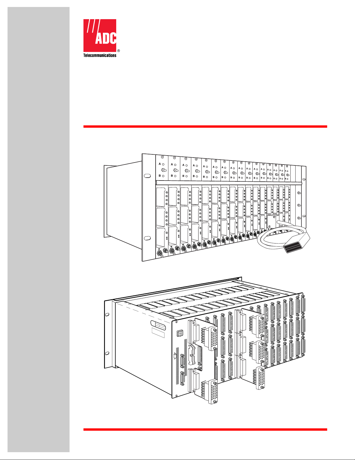
2.1 PatchSwitch Assembly Configurations . . . . . . . . . . . . . . . . . . . . . . . . . . . . . . . . . . . . . . . . . . . . . . . . . . . . . . . . . . . . . . . . . 1-2
2.2 PatchSwitch Equipment. . . . . . . . . . . . . . . . . . . . . . . . . . . . . . . . . . . . . . . . . . . . . . . . . . . . . . . . . . . . . . . . . . . . . . . . . . . . . . 1-5
3 SPECIFICATIONS . . . . . . . . . . . . . . . . . . . . . . . . . . . . . . . . . . . . . . . . . . . . . . . . . . . . . . . . . . . . . . . . . . . . . . . . . . . . . . . . . . . . . . . . . . 1-9
3.1 DMPS-10 AC Power Supply. . . . . . . . . . . . . . . . . . . . . . . . . . . . . . . . . . . . . . . . . . . . . . . . . . . . . . . . . . . . . . . . . . . . . . . . . . . 1-9
1 GENERAL. . . . . . . . . . . . . . . . . . . . . . . . . . . . . . . . . . . . . . . . . . . . . . . . . . . . . . . . . . . . . . . . . . . . . . . . . . . . . . . . . . . . . . . . . . . . . . . . . 2-1
2 PATCHING WITH IN-LINE A/B SWITCHING. . . . . . . . . . . . . . . . . . . . . . . . . . . . . . . . . . . . . . . . . . . . . . . . . . . . . . . . . . . . . . . . . . . . . . 2-1
3 A/B SWITCHING WITH OFF-LINE MONITOR ACCESS. . . . . . . . . . . . . . . . . . . . . . . . . . . . . . . . . . . . . . . . . . . . . . . . . . . . . . . . . . . . . 2-2
3.1 PS Control Module (RDM-15). . . . . . . . . . . . . . . . . . . . . . . . . . . . . . . . . . . . . . . . . . . . . . . . . . . . . . . . . . . . . . . . . . . . . . . . . . 2-3
3.2 LED/Alarm Patch Module with A/B Switching and In-Line Patch Access (PSM-01) . . . . . . . . . . . . . . . . . . . . . . . . . . . . . 2-7
3.3 Patch Module with A/B Switching and In-Line Patch Access (PSM-02) . . . . . . . . . . . . . . . . . . . . . . . . . . . . . . . . . . . . . . 2-12
4 A/B SWITCHING MODULE (PSM-03) . . . . . . . . . . . . . . . . . . . . . . . . . . . . . . . . . . . . . . . . . . . . . . . . . . . . . . . . . . . . . . . . . . . . . . . . . . 2-13
5 LED/ALARM PATCH MODULE WITH A/B SWITCHING AND OFF-LINE ACCESS (PSM-04) . . . . . . . . . . . . . . . . . . . . . . . . . . . . . . 2-14
6 PATCH MODULE WITH A/B SWITCHING AND OFF-LINE ACCESS (PSM-05) . . . . . . . . . . . . . . . . . . . . . . . . . . . . . . . . . . . . . . . . . 2-14
7 LED/ALARM PATCH INTERFACE (PSM-07) . . . . . . . . . . . . . . . . . . . . . . . . . . . . . . . . . . . . . . . . . . . . . . . . . . . . . . . . . . . . . . . . . . . . 2-14
7.1 Patch Interface (PSM-08) . . . . . . . . . . . . . . . . . . . . . . . . . . . . . . . . . . . . . . . . . . . . . . . . . . . . . . . . . . . . . . . . . . . . . . . . . . . . 2-15
8 TEST MODULE (PSM-12) . . . . . . . . . . . . . . . . . . . . . . . . . . . . . . . . . . . . . . . . . . . . . . . . . . . . . . . . . . . . . . . . . . . . . . . . . . . . . . . . . . . 2-16
9 TEST MODULE (PSM 13) . . . . . . . . . . . . . . . . . . . . . . . . . . . . . . . . . . . . . . . . . . . . . . . . . . . . . . . . . . . . . . . . . . . . . . . . . . . . . . . . . . . 2-17
10 PS RS-422/RS-232 INTERFACE CONVERTER MODULE (PSR-06) . . . . . . . . . . . . . . . . . . . . . . . . . . . . . . . . . . . . . . . . . . . . . . . . . . 2-18
11 PS CHASSIS POWER . . . . . . . . . . . . . . . . . . . . . . . . . . . . . . . . . . . . . . . . . . . . . . . . . . . . . . . . . . . . . . . . . . . . . . . . . . . . . . . . . . . . . . 2-19
ADCP-50-304 • Issue 19 • June 1999 • Pre fa ce
SECTION 1
INTRODUCTION
SECTION 2
FUNCTIONAL DESCRIPTION
SECTION 3
PATCHSWITCH V.35
1 PRODUCT OFFERING. . . . . . . . . . . . . . . . . . . . . . . . . . . . . . . . . . . . . . . . . . . . . . . . . . . . . . . . . . . . . . . . . . . . . . . . . . . . . . . . . . . . . . . 3-1
2 APPLICATION WITH EXISTING UNITS . . . . . . . . . . . . . . . . . . . . . . . . . . . . . . . . . . . . . . . . . . . . . . . . . . . . . . . . . . . . . . . . . . . . . . . . . 3-2
3 FUNCTION SELECTION-MODULES. . . . . . . . . . . . . . . . . . . . . . . . . . . . . . . . . . . . . . . . . . . . . . . . . . . . . . . . . . . . . . . . . . . . . . . . . . . . 3-4
4 FUNCTIONAL SELECTION—CONVERSION BOARD . . . . . . . . . . . . . . . . . . . . . . . . . . . . . . . . . . . . . . . . . . . . . . . . . . . . . . . . . . . . . . 3-5
5 HARDWARE INSTALLATION . . . . . . . . . . . . . . . . . . . . . . . . . . . . . . . . . . . . . . . . . . . . . . . . . . . . . . . . . . . . . . . . . . . . . . . . . . . . . . . . . 3-8
6 RECOMMENDED MATING CONNECTOR PARTS. . . . . . . . . . . . . . . . . . . . . . . . . . . . . . . . . . . . . . . . . . . . . . . . . . . . . . . . . . . . . . . . . 3-9
© 1999, ADC Telecommunications, Inc.
Page iii
Page 4

ADCP-50-304 • Issue 19 • June 1999 • Preface
TABLE OF CONTENTS
Content Page
1 GENERAL. . . . . . . . . . . . . . . . . . . . . . . . . . . . . . . . . . . . . . . . . . . . . . . . . . . . . . . . . . . . . . . . . . . . . . . . . . . . . . . . . . . . . . . . . . . . . . . . . 4-1
2 DESCRIPTION . . . . . . . . . . . . . . . . . . . . . . . . . . . . . . . . . . . . . . . . . . . . . . . . . . . . . . . . . . . . . . . . . . . . . . . . . . . . . . . . . . . . . . . . . . . . . 4-2
2.1 PSM-812001 X.21 LED/Alarm Patch Module with A/B Switching and Off-Line Patch Access . . . . . . . . . . . . . . . . . . . . . 4-2
2.2 PSM-813001 X.21 PatchSwitch Module with A/B Switching and Off-Line Patch Access . . . . . . . . . . . . . . . . . . . . . . . . . 4-3
2.3 PSM-832001 X.21 LED/Alarm PatchSwitch Interface Module. . . . . . . . . . . . . . . . . . . . . . . . . . . . . . . . . . . . . . . . . . . . . . . . 4-3
2.4 PSM-83301 X.21 PatchSwitch Module . . . . . . . . . . . . . . . . . . . . . . . . . . . . . . . . . . . . . . . . . . . . . . . . . . . . . . . . . . . . . . . . . . 4-4
2.5 PSM-832002 X.21 LED/Alarm PatchSwitch Test/Status Module . . . . . . . . . . . . . . . . . . . . . . . . . . . . . . . . . . . . . . . . . . . . . 4-4
2.6 PSO-839001 Backplane Adapter Module . . . . . . . . . . . . . . . . . . . . . . . . . . . . . . . . . . . . . . . . . . . . . . . . . . . . . . . . . . . . . . . . 4-5
2.7 PSO-836001 Backplane Adapter Module . . . . . . . . . . . . . . . . . . . . . . . . . . . . . . . . . . . . . . . . . . . . . . . . . . . . . . . . . . . . . . . . 4-5
2.8 PSO-839002 Backplane Adapter Module . . . . . . . . . . . . . . . . . . . . . . . . . . . . . . . . . . . . . . . . . . . . . . . . . . . . . . . . . . . . . . . . 4-5
3 FUNCTIONAL DESCRIPTION. . . . . . . . . . . . . . . . . . . . . . . . . . . . . . . . . . . . . . . . . . . . . . . . . . . . . . . . . . . . . . . . . . . . . . . . . . . . . . . . . 4-5
3.1 A/B Switch Modules. . . . . . . . . . . . . . . . . . . . . . . . . . . . . . . . . . . . . . . . . . . . . . . . . . . . . . . . . . . . . . . . . . . . . . . . . . . . . . . . . 4-5
3.2 Switch Module Interlocks . . . . . . . . . . . . . . . . . . . . . . . . . . . . . . . . . . . . . . . . . . . . . . . . . . . . . . . . . . . . . . . . . . . . . . . . . . . . 4-6
3.3 Monitor, Patch, and Access Modules. . . . . . . . . . . . . . . . . . . . . . . . . . . . . . . . . . . . . . . . . . . . . . . . . . . . . . . . . . . . . . . . . . . 4-6
3.4 Status Indication Modules. . . . . . . . . . . . . . . . . . . . . . . . . . . . . . . . . . . . . . . . . . . . . . . . . . . . . . . . . . . . . . . . . . . . . . . . . . . . 4-7
3.5 Alarm Modules . . . . . . . . . . . . . . . . . . . . . . . . . . . . . . . . . . . . . . . . . . . . . . . . . . . . . . . . . . . . . . . . . . . . . . . . . . . . . . . . . . . . . 4-7
3.6 Alarm Reset . . . . . . . . . . . . . . . . . . . . . . . . . . . . . . . . . . . . . . . . . . . . . . . . . . . . . . . . . . . . . . . . . . . . . . . . . . . . . . . . . . . . . . . 4-7
3.7 Alarm Time Delay . . . . . . . . . . . . . . . . . . . . . . . . . . . . . . . . . . . . . . . . . . . . . . . . . . . . . . . . . . . . . . . . . . . . . . . . . . . . . . . . . . . 4-8
3.8 B Alarm Enable/Disable. . . . . . . . . . . . . . . . . . . . . . . . . . . . . . . . . . . . . . . . . . . . . . . . . . . . . . . . . . . . . . . . . . . . . . . . . . . . . . 4-9
3.9 PSM-832002 Module Quiescent State Indicators . . . . . . . . . . . . . . . . . . . . . . . . . . . . . . . . . . . . . . . . . . . . . . . . . . . . . . . . . 4-9
4 POWER REQUIREMENTS. . . . . . . . . . . . . . . . . . . . . . . . . . . . . . . . . . . . . . . . . . . . . . . . . . . . . . . . . . . . . . . . . . . . . . . . . . . . . . . . . . . . 4-9
5 SPECIFICATIONS . . . . . . . . . . . . . . . . . . . . . . . . . . . . . . . . . . . . . . . . . . . . . . . . . . . . . . . . . . . . . . . . . . . . . . . . . . . . . . . . . . . . . . . . . 4-10
6 INSTALLATION . . . . . . . . . . . . . . . . . . . . . . . . . . . . . . . . . . . . . . . . . . . . . . . . . . . . . . . . . . . . . . . . . . . . . . . . . . . . . . . . . . . . . . . . . . . 4-10
6.1 Interlock Jumper Installation . . . . . . . . . . . . . . . . . . . . . . . . . . . . . . . . . . . . . . . . . . . . . . . . . . . . . . . . . . . . . . . . . . . . . . . . 4-10
6.2 Alarm Jumper Installation. . . . . . . . . . . . . . . . . . . . . . . . . . . . . . . . . . . . . . . . . . . . . . . . . . . . . . . . . . . . . . . . . . . . . . . . . . . 4-11
6.3 Alarm Time Delay Setting . . . . . . . . . . . . . . . . . . . . . . . . . . . . . . . . . . . . . . . . . . . . . . . . . . . . . . . . . . . . . . . . . . . . . . . . . . . 4-12
6.4 Adapter Installation . . . . . . . . . . . . . . . . . . . . . . . . . . . . . . . . . . . . . . . . . . . . . . . . . . . . . . . . . . . . . . . . . . . . . . . . . . . . . . . . 4-12
6.5 Module Installation. . . . . . . . . . . . . . . . . . . . . . . . . . . . . . . . . . . . . . . . . . . . . . . . . . . . . . . . . . . . . . . . . . . . . . . . . . . . . . . . . 4-12
6.6 Cable Connections. . . . . . . . . . . . . . . . . . . . . . . . . . . . . . . . . . . . . . . . . . . . . . . . . . . . . . . . . . . . . . . . . . . . . . . . . . . . . . . . . 4-12
SECTION 4
PATCHSWITCH X.21
1 GENERAL. . . . . . . . . . . . . . . . . . . . . . . . . . . . . . . . . . . . . . . . . . . . . . . . . . . . . . . . . . . . . . . . . . . . . . . . . . . . . . . . . . . . . . . . . . . . . . . . . 5-1
2 SPACE REQUIREMENTS . . . . . . . . . . . . . . . . . . . . . . . . . . . . . . . . . . . . . . . . . . . . . . . . . . . . . . . . . . . . . . . . . . . . . . . . . . . . . . . . . . . . 5-1
3 ENVIRONMENTAL CONSIDERATIONS . . . . . . . . . . . . . . . . . . . . . . . . . . . . . . . . . . . . . . . . . . . . . . . . . . . . . . . . . . . . . . . . . . . . . . . . . 5-1
4 POWER REQUIREMENTS. . . . . . . . . . . . . . . . . . . . . . . . . . . . . . . . . . . . . . . . . . . . . . . . . . . . . . . . . . . . . . . . . . . . . . . . . . . . . . . . . . . . 5-1
Page iv
© 1999, ADC Telecommunications, Inc.
SECTION 5
SITE PREPARATION
Page 5

TABLE OF CONTENTS
Content Page
1 GENERAL. . . . . . . . . . . . . . . . . . . . . . . . . . . . . . . . . . . . . . . . . . . . . . . . . . . . . . . . . . . . . . . . . . . . . . . . . . . . . . . . . . . . . . . . . . . . . . . . . 6-1
1.1 PatchSwitch Chassis Installation (For PatchSwitch V.35 Installation, see Section 3) . . . . . . . . . . . . . . . . . . . . . . . . . . . 6-1
1.2 PatchSwitch Module Installation Procedure . . . . . . . . . . . . . . . . . . . . . . . . . . . . . . . . . . . . . . . . . . . . . . . . . . . . . . . . . . . . . 6-2
1.3 Blank Panel Installation. . . . . . . . . . . . . . . . . . . . . . . . . . . . . . . . . . . . . . . . . . . . . . . . . . . . . . . . . . . . . . . . . . . . . . . . . . . . . . 6-2
1.4 Chassis Power Supply Connection Procedure . . . . . . . . . . . . . . . . . . . . . . . . . . . . . . . . . . . . . . . . . . . . . . . . . . . . . . . . . . . 6-2
1.5 Communications Network Interface Connections . . . . . . . . . . . . . . . . . . . . . . . . . . . . . . . . . . . . . . . . . . . . . . . . . . . . . . . . 6-3
1.6 Control Module DIP Switch Settings . . . . . . . . . . . . . . . . . . . . . . . . . . . . . . . . . . . . . . . . . . . . . . . . . . . . . . . . . . . . . . . . . . . 6-4
2 CONTROL MODULE AUTOFALLBACK JUMPER INSTALLATION . . . . . . . . . . . . . . . . . . . . . . . . . . . . . . . . . . . . . . . . . . . . . . . . . . . 6-6
3 CONTROL MODULE REMOTE CONTROL JUMPER INSTALLATION . . . . . . . . . . . . . . . . . . . . . . . . . . . . . . . . . . . . . . . . . . . . . . . . . 6-7
4 PS MODULE JUMPER INSTALLATION . . . . . . . . . . . . . . . . . . . . . . . . . . . . . . . . . . . . . . . . . . . . . . . . . . . . . . . . . . . . . . . . . . . . . . . . . 6-8
4.1 Interlock Jumper Installation. . . . . . . . . . . . . . . . . . . . . . . . . . . . . . . . . . . . . . . . . . . . . . . . . . . . . . . . . . . . . . . . . . . . . . . . . . 6-8
4.2 Alarm Jumper Installation . . . . . . . . . . . . . . . . . . . . . . . . . . . . . . . . . . . . . . . . . . . . . . . . . . . . . . . . . . . . . . . . . . . . . . . . . . . . 6-8
4.3 Automatic Alarm Reset Jumper Installation . . . . . . . . . . . . . . . . . . . . . . . . . . . . . . . . . . . . . . . . . . . . . . . . . . . . . . . . . . . . . 6-9
ADCP-50-304 • Issue 19 • June 1999 • Pre fa ce
SECTION 6
INSTALLATION
SECTION 7
OPERATION
1 GENERAL. . . . . . . . . . . . . . . . . . . . . . . . . . . . . . . . . . . . . . . . . . . . . . . . . . . . . . . . . . . . . . . . . . . . . . . . . . . . . . . . . . . . . . . . . . . . . . . . . 7-2
2 PATCHING — IN-LINE ACCESS MODULES . . . . . . . . . . . . . . . . . . . . . . . . . . . . . . . . . . . . . . . . . . . . . . . . . . . . . . . . . . . . . . . . . . . . . 7-2
2.1 Monitor Patching . . . . . . . . . . . . . . . . . . . . . . . . . . . . . . . . . . . . . . . . . . . . . . . . . . . . . . . . . . . . . . . . . . . . . . . . . . . . . . . . . . . 7-2
2.2 Intrusive Patching . . . . . . . . . . . . . . . . . . . . . . . . . . . . . . . . . . . . . . . . . . . . . . . . . . . . . . . . . . . . . . . . . . . . . . . . . . . . . . . . . . 7-2
3 PATCHING — OFF-LINE ACCESS MODULES . . . . . . . . . . . . . . . . . . . . . . . . . . . . . . . . . . . . . . . . . . . . . . . . . . . . . . . . . . . . . . . . . . . 7-2
4 INTERFACE MODULE. . . . . . . . . . . . . . . . . . . . . . . . . . . . . . . . . . . . . . . . . . . . . . . . . . . . . . . . . . . . . . . . . . . . . . . . . . . . . . . . . . . . . . . 7-3
4.1 Test Module. . . . . . . . . . . . . . . . . . . . . . . . . . . . . . . . . . . . . . . . . . . . . . . . . . . . . . . . . . . . . . . . . . . . . . . . . . . . . . . . . . . . . . . . 7-3
5 SWITCHING . . . . . . . . . . . . . . . . . . . . . . . . . . . . . . . . . . . . . . . . . . . . . . . . . . . . . . . . . . . . . . . . . . . . . . . . . . . . . . . . . . . . . . . . . . . . . . . 7-3
6 CONTROL MODULE SWITCHING (LOCAL). . . . . . . . . . . . . . . . . . . . . . . . . . . . . . . . . . . . . . . . . . . . . . . . . . . . . . . . . . . . . . . . . . . . . . 7-4
6.1 Interface Converter Module (PSR-06A) . . . . . . . . . . . . . . . . . . . . . . . . . . . . . . . . . . . . . . . . . . . . . . . . . . . . . . . . . . . . . . . . . 7-4
6.2 Single Channel Switching . . . . . . . . . . . . . . . . . . . . . . . . . . . . . . . . . . . . . . . . . . . . . . . . . . . . . . . . . . . . . . . . . . . . . . . . . . . . 7-4
6.3 Bank Switching. . . . . . . . . . . . . . . . . . . . . . . . . . . . . . . . . . . . . . . . . . . . . . . . . . . . . . . . . . . . . . . . . . . . . . . . . . . . . . . . . . . . . 7-5
6.4 Reset Alarms. . . . . . . . . . . . . . . . . . . . . . . . . . . . . . . . . . . . . . . . . . . . . . . . . . . . . . . . . . . . . . . . . . . . . . . . . . . . . . . . . . . . . . . 7-5
6.5 DC Pulse Control Switching . . . . . . . . . . . . . . . . . . . . . . . . . . . . . . . . . . . . . . . . . . . . . . . . . . . . . . . . . . . . . . . . . . . . . . . . . . 7-5
6.6 Remote Control Switching. . . . . . . . . . . . . . . . . . . . . . . . . . . . . . . . . . . . . . . . . . . . . . . . . . . . . . . . . . . . . . . . . . . . . . . . . . . . 7-6
6.7 Remote Control Commands . . . . . . . . . . . . . . . . . . . . . . . . . . . . . . . . . . . . . . . . . . . . . . . . . . . . . . . . . . . . . . . . . . . . . . . . . . 7-6
6.8 Command Conventions. . . . . . . . . . . . . . . . . . . . . . . . . . . . . . . . . . . . . . . . . . . . . . . . . . . . . . . . . . . . . . . . . . . . . . . . . . . . . . 7-6
6.9 Command Flags . . . . . . . . . . . . . . . . . . . . . . . . . . . . . . . . . . . . . . . . . . . . . . . . . . . . . . . . . . . . . . . . . . . . . . . . . . . . . . . . . . . . 7-7
6.10 Command Interpretation . . . . . . . . . . . . . . . . . . . . . . . . . . . . . . . . . . . . . . . . . . . . . . . . . . . . . . . . . . . . . . . . . . . . . . . . . . . . . 7-7
6.11 Command Responses . . . . . . . . . . . . . . . . . . . . . . . . . . . . . . . . . . . . . . . . . . . . . . . . . . . . . . . . . . . . . . . . . . . . . . . . . . . . . . . 7-8
6.12 Command Descriptions. . . . . . . . . . . . . . . . . . . . . . . . . . . . . . . . . . . . . . . . . . . . . . . . . . . . . . . . . . . . . . . . . . . . . . . . . . . . . . 7-8
6.13 Select PS Chassis Command . . . . . . . . . . . . . . . . . . . . . . . . . . . . . . . . . . . . . . . . . . . . . . . . . . . . . . . . . . . . . . . . . . . . . . . . . 7-9
6.14 GO Command . . . . . . . . . . . . . . . . . . . . . . . . . . . . . . . . . . . . . . . . . . . . . . . . . . . . . . . . . . . . . . . . . . . . . . . . . . . . . . . . . . . . . . 7-9
© 1999, ADC Telecommunications, Inc.
Page v
Page 6

ADCP-50-304 • Issue 19 • June 1999 • Preface
TABLE OF CONTENTS
Content Page
6.15 Request Software Revision Level (REV) Command) . . . . . . . . . . . . . . . . . . . . . . . . . . . . . . . . . . . . . . . . . . . . . . . . . . . . . 7-10
6.16 Request Status (UPdate Command). . . . . . . . . . . . . . . . . . . . . . . . . . . . . . . . . . . . . . . . . . . . . . . . . . . . . . . . . . . . . . . . . . . 7-10
6.17 Status Responses . . . . . . . . . . . . . . . . . . . . . . . . . . . . . . . . . . . . . . . . . . . . . . . . . . . . . . . . . . . . . . . . . . . . . . . . . . . . . . . . . 7-10
6.18 TLKxx Format. . . . . . . . . . . . . . . . . . . . . . . . . . . . . . . . . . . . . . . . . . . . . . . . . . . . . . . . . . . . . . . . . . . . . . . . . . . . . . . . . . . . . 7-10
6.19 TLKxx Execution . . . . . . . . . . . . . . . . . . . . . . . . . . . . . . . . . . . . . . . . . . . . . . . . . . . . . . . . . . . . . . . . . . . . . . . . . . . . . . . . . . 7-12
6.20 SPKxx Format. . . . . . . . . . . . . . . . . . . . . . . . . . . . . . . . . . . . . . . . . . . . . . . . . . . . . . . . . . . . . . . . . . . . . . . . . . . . . . . . . . . . . 7-18
6.21 Reset Alarm Status (IN Command). . . . . . . . . . . . . . . . . . . . . . . . . . . . . . . . . . . . . . . . . . . . . . . . . . . . . . . . . . . . . . . . . . . . 7-19
6.22 Enable/Disable Alarm Status Reporting (AL Command) . . . . . . . . . . . . . . . . . . . . . . . . . . . . . . . . . . . . . . . . . . . . . . . . . . 7-19
6.23 Request Switching (AB Command). . . . . . . . . . . . . . . . . . . . . . . . . . . . . . . . . . . . . . . . . . . . . . . . . . . . . . . . . . . . . . . . . . . 7-20
6.24 Request Super Chassis Command (SC Command) . . . . . . . . . . . . . . . . . . . . . . . . . . . . . . . . . . . . . . . . . . . . . . . . . . . . . . 7-22
6.25 De-Select The PS Chassis (UNT) . . . . . . . . . . . . . . . . . . . . . . . . . . . . . . . . . . . . . . . . . . . . . . . . . . . . . . . . . . . . . . . . . . . . . 7-23
6.26 Error Codes . . . . . . . . . . . . . . . . . . . . . . . . . . . . . . . . . . . . . . . . . . . . . . . . . . . . . . . . . . . . . . . . . . . . . . . . . . . . . . . . . . . . . . 7-23
6.27 Testing The Communications Line. . . . . . . . . . . . . . . . . . . . . . . . . . . . . . . . . . . . . . . . . . . . . . . . . . . . . . . . . . . . . . . . . . . . 7-24
SECTION 8
GENERAL INFORMATION
1 WARRANTY/SOFTWARE . . . . . . . . . . . . . . . . . . . . . . . . . . . . . . . . . . . . . . . . . . . . . . . . . . . . . . . . . . . . . . . . . . . . . . . . . . . . . . . . . . . . 8-1
2 REPAIR/ADVANCE REPLACEMENT POLICY. . . . . . . . . . . . . . . . . . . . . . . . . . . . . . . . . . . . . . . . . . . . . . . . . . . . . . . . . . . . . . . . . . . . 8-1
3 REPAIR CHARGES . . . . . . . . . . . . . . . . . . . . . . . . . . . . . . . . . . . . . . . . . . . . . . . . . . . . . . . . . . . . . . . . . . . . . . . . . . . . . . . . . . . . . . . . . 8-2
4 REPLACEMENT/SPARE PRODUCTS . . . . . . . . . . . . . . . . . . . . . . . . . . . . . . . . . . . . . . . . . . . . . . . . . . . . . . . . . . . . . . . . . . . . . . . . . . 8-2
5 RETURNED MATERIAL. . . . . . . . . . . . . . . . . . . . . . . . . . . . . . . . . . . . . . . . . . . . . . . . . . . . . . . . . . . . . . . . . . . . . . . . . . . . . . . . . . . . . . 8-2
6 CUSTOMER INFORMATION AND ASSISTANCE . . . . . . . . . . . . . . . . . . . . . . . . . . . . . . . . . . . . . . . . . . . . . . . . . . . . . . . . . . . . . . . . . 8-3
Page vi
© 1999, ADC Telecommunications, Inc.
Page 7

REVISION HISTORY
EDITION/ISSUE DATE REASON FOR CHANGE
1st Edition, Issue 1 02/83 Original.
1st Edition, Issue 2 03/83 Technical changes.
1st Edition, Issue 3 03/83 Warranty changes.
1st Edition, Issue 4 07/83 Technical changes.
2nd Edition, Issue 1 02/84 Incorporation of remote control.
2nd Edition, Issue 2 10/84 Technical changes.
3rd Edition, Issue 1 03/86 Incorporated PSM-12 and PSM-13 Test Modules.
3rd Edition, Issue 2 05/86 Edited Com munications Network Interface Connections paragraph for clarification an d
4th Edition, Issue 1 07/86 Incorporated PSM-1 2 and PSM-13 Test Modules. Added autofailback feature and super
5th Edition, Issue 1 12/86 Delete references to PSM-14 CTRL Module.
6th Edition, Issue 1 06/88 Technical changes and clarification.
7th Edition, Issue 1 10/88 Added V.35 modules and conversion boards.
7th Edition, Issue 2 08/89 Changed Figure 3-6.
8th Edition, Issue 1 05/90 Added new information on PSM-15.
8th Edition, Issue 2 06/90 Ch an ged DIP Switch Settings in Figure 5-3 and in Control Module DIP Switch Set ti ngs
9th Edition, Issue 1 09/91 General technical changes and added X.21 modul es.
9th Edition, Issue 2 05/92 Add ed DMP S-10 Power Supply.
10th Edition, Issue 1 03/93 Added DC control.
Issue 19 06/99 Update to current forma t st andards.
ADCP-50-304 • Issue 19 • June 1999 • Pre fa ce
corrected connect ors designations in Figure 4-1.
chassis selection (SC comman d) to Remote Control Module, st at us response for TLK
(terminal) selection, and Ver tical interlock to PSM-01, PSM-02, and PSM-03. Added PSM04, PSM-05 Patch Modules with off-line access, and RS-422/RS-232 Data Converter Module.
paragraph.
ABOUT THIS MANUAL
This user manual describes the RS-232/V.24 and V.35 PatchSwitch equipment. The manual
provides information necessary to install and operate these units. The manual is intended fo r use
at communications network facilities and users who monitor and maintain the network. Section 1
provides a general description of the ADC equipment. Section 2 provides a functional
description of the equipment components. Section 3 provides a complete description of V.35
modules. Section 4 provides a description of X.21 modules. Sections 5 and 6 describe the
equipment site preparation an d installation. Sectio n 7 describes the op eration of the equipm ent.
General Information Section explains the equipment warranty, repair/exchange policy, charges,
replacement/spare parts, returned material and customer suppor t services.
Portions of the Patch Modules are covered by U.S. Pat. No. 4,363,941 and corresponding
foreign Letters Patent.
© 1999, ADC Telecommunications, Inc.
Page vii
Page 8

ADCP-50-304 • Issue 19 • June 1999 • Preface
RELATED PUBLICATIONS
Listed below are all the related manuals, their content, and their publication numbers. Copies of
these publications can be ordered by contacting the ADC Technical Assistance Center at
1-800-366-3891 (in U.S.A. or Canada) or 612-946-3000, extension 3223 (outside U.S.A. and
Canada.
Title ADCP Number
Network Control Products Catalog 517
PatchSwitch Remote Control Unit User Manual ADCP-50-302
PatchSwitch V.35 Installation and User Guide ADCP-50-311
Remote Test Access (RTA) Espion 500 System User Manual ADCP-50-100
Remote Test Access (RTA) System User Manual ADCP-50-101
ADMONISHMENTS
Important safety admoni shmen ts are used throughou t thi s manual to warn of possi ble haza rds to
persons or equipment. An admonishment identifies a possible hazard and then explains what
may happen if the hazard is not avoided. The admonishments — in the form of Dangers,
Warnings, and Cautions — must be followed at all times. These warnings are flagged by use of
the triangular alert icon (seen below), and are listed in descending order of severity of injury or
damage and likelihood of occurrence.
Danger: Danger is used to indicate the presence of a hazard that will cause severe personal
injury, death, or substantial property damage if the hazard is not avoided.
Warning: Warning is used to indicate the presence of a hazard that can cause severe personal
injury, death, or substantial property damage if the hazard is not avoided.
Caution: Caution is used to indicate the presence of a hazard that will or can cause minor
personal injury or property damage if the hazard is not avoided.
Page viii
© 1999, ADC Telecommunications, Inc.
Page 9

GENERAL SAFETY PRECAUTIONS
Danger: To prevent electrical shock, never install telephone equipment in a wet location or
during a lightning storm. When installing or modifying telephone lines, disconnect lines on the
network side before working with uninsulated lines or terminals.
Danger: The chassis must be properly grounded to ensure equipment and human safety.
Danger: Electric modules can be damaged by electrostatic discharge (ESD). Before handling
modules, wear an anti-static discharge wrist strap to prevent damage to electronic components.
Place modules in anti-static packing material when transporting or storing. When working on
modules, always place them on an approved anti-static mat that is electrically grounded.
FCC COMPLIANCE STATEMENT
This product has been certified to comply with the requirements for class A computing devices
per part 15 of the FCC regulations.
ADCP-50-304 • Issue 19 • June 1999 • Pre fa ce
Danger: This equipment generates, uses, and can radiate radio frequency energy and if not
installed and used in accordance with the user manual, may cause interference to radio
communications. It has been tested and found to comply with limits for a Class B computing
device pursuant to Subpart J of Part 15 of FCC Rules, which are designed to provide reasonable
protection against such interference when operated in a commercial environment. Operation of
this equipment in a residential area is likely to cause interference in which case the user, at his
own expense, will be required to take whatever measures may be required to correct the
interference.
© 1999, ADC Telecommunications, Inc.
Page ix
Page 10

INTRODUCTION
Page 11

SECTION 1: INTRODUCTION
Content Page
1 GENERAL. . . . . . . . . . . . . . . . . . . . . . . . . . . . . . . . . . . . . . . . . . . . . . . . . . . . . . . . . . . . . . . . . . . . . . . . . . . .1-1
2 PURPOSE AND SCOPE . . . . . . . . . . . . . . . . . . . . . . . . . . . . . . . . . . . . . . . . . . . . . . . . . . . . . . . . . . . . . . . . . . .1-2
2.1 PatchSwitch Assembly Configurations . . . . . . . . . . . . . . . . . . . . . . . . . . . . . . . . . . . . . . . . . . . . . . . . . .1-2
2.2 PatchSwitch Equipment . . . . . . . . . . . . . . . . . . . . . . . . . . . . . . . . . . . . . . . . . . . . . . . . . . . . . . . . . . . .1- 5
3 SPECIFICATIONS. . . . . . . . . . . . . . . . . . . . . . . . . . . . . . . . . . . . . . . . . . . . . . . . . . . . . . . . . . . . . . . . . . . . . . .1-9
3.1 DMPS-10 AC Power Supply. . . . . . . . . . . . . . . . . . . . . . . . . . . . . . . . . . . . . . . . . . . . . . . . . . . . . . . . . .1-9
_________________ ___________________ ______________________________________ _______________________________
1 GENERAL
ADC PatchSwitch Digital Patching with RS-232/V.24, X.21, and V.35 Switching equipment,
hereinafter refe rr ed t o a s PatchSwitch or PS, p rovides conveni ent ac ces s t o RS- 232 (ANSI/EIA-
232) or CCITT V.24, X.21, or V.35 circuits for patching or switching to allow monitoring,
testing, and reconfiguring of a communications network. The V.35 description is located in
Section 3. The X.21 description is located in Section 4.
ADCP-50-304 • Issue 19 • June 199 9 • Sec tion 1: In troduction
Note:
The PatchSwitch equipment described in this manual conforms to EIA/CCITT (RS232/Recommendation V.24), interfa ce between Data Terminal Equipment (DTE) and Data
Communication Equipment (DCE) known as the Serial Binary Data Int er change or SBDI.
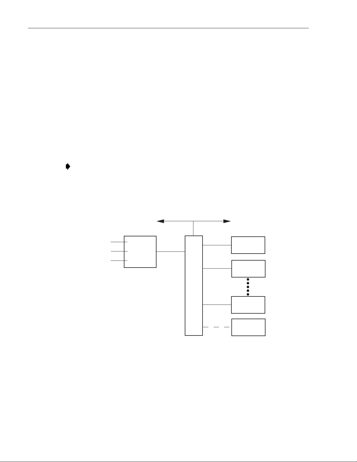
The PatchSwitch product line is a flexible, modular system providing the following features:
1. Monitoring of digital communications leads without circuit interruption;
2. Line access and switching on data communications circuit directed toward two (A/B)
equipments at the DTE end and as directed toward the modem at the DCE end;
3. Loss of monitored signal alarming circuits which identify the down circuit with either or
both visual and audible indications;
4. Optional signal monitoring and alarming of eight different RS-232 signal lines;
5. Optional interlocking in groups of two to 16 modules with A/B switching;
6. Optional interlocking in groups of two to 16 chassis with A/B switching;
7. Optional test module with three (3) RS-232 female ports for convenient interface with
compatible test equipment, with or without lead status monitoring LEDs (8-leads
monitored);
8. Flexibility of t he modular system appr oach al lo ws th e additi on of chas sis and modul es and
the interchange of modules on a single line basis;
9. Module replacement or removal with no need for rear cable disconnection;
10. All female DTE and DCE connectors or female DTE and male DCE connectors;
11. High density chassis occupies 7 inches (17.78 cm) in height within a standard 19-inch
(48.26 cm) wide rack;
© 1999, ADC Telecommunications, Inc.
Page 1-1
Page 12

ADCP-50-304 • Issue 19 • June 1999 • Section 1: Introduction
12. Remote switching and alarm c ontrol opera tion up to 1,0 00 fee t a way from t he P at chSwit ch
chassis rack;
13. Remote operator control via ser ial da ta communic ation s circ uits e mploy ing eit her RS-2 32,
RS-422 or V.35 standards;
14. Optional autofallback to either A/B switch position on detection of an alarm;
15. Local or remote bank switching using manual or serial control;
16. 0, +5V and –5 to –48 Vdc pulse controlled bank switching, and
17. Direct test access to off-line devices.
2 PURPOSE AND SCOPE
The purpose of this manual is to provide the user with information necessary to install and
operate the PatchSwitch equipment. Section 1 is a general description of the PatchSwitch
equipment.
2.1 PatchSwitch Assembly Configurations
Prepackaged standard product PS assemblies are configured as listed in Table 1-1. All
assemblies contain 16 PS modules in the leftmost 16 positions of the 18 position chassis. The
17th position contains a blank panel and the 18th position contains the PS Chassis Control
Module. Each of the 16 modules provides patching and/or A/B (A channel DTE or B channel
DTE) fallback switching for all 23 leads of an RS-232/V.24 or V.35 circuit. Bank switching,
switching operation enab le, and mast er ala rm reset are al l pro vid ed for in t he Control Module of
the PS Chassis. Each module may be configured as part of an interlocked group.
Only one module of an interlock ed gr oup can be in the B stat e at one time. Eac h ass embly has a
blank designation strip for operator labeling of the circuits. The PS assembly has two main
functions. First, it allows a user to select from two DTE channels to be connected to a DCE.
Secondly, it allows the user to monitor and restore data channels through the use of manual
patching. The PS assembly gives positive indication of the current DTE channel in use and
allows the operato r to switch all 16 channel s in the PS assembly with a si ngle switch (bank
switch). With user selectable serial remote control, the switching function can be located up to
1,000 feet away for the PS chassis assembly. With user selectable dc controlled bank switching,
the bank switching function can be located up to 500 feet away.
Page 1-2
© 1999, ADC Telecommunications, Inc.
Page 13

ADCP-50-304 • Issue 19 • June 199 9 • Sec tion 1: In troduction
The Interlocked group feature protects a device used as a substitute. A spare device may be
connected to the DTE-B port of several A/B switching modules as shown in Figure 1-1. The A/B
Interlock Jumper of each module in the group m ust be in the same position. When one device
fails, the spare device may be substituted. Now, If another device fails, the interlocked group
feature prevents the spare from being substituted for the second failed device.
Table 1-1. PatchSwitch (PS) Assembly Configurations
ADC
NUMBER DESCRIPTION
PSA-01
RS-232 16 Line LED/Alarm Patching with A/B Switching
(Female DTE/DCE Connectors
)
PSA-02 RS-232 16 Line LED/Alarm Patching with A/B Switching
(Female DTE and Male DCE Connectors)
PSA-03 RS-232 16 Line Patching with A/B Switching
(Female DTE/DCE Connectors)
PSA-04 RS-232 16 Line Patching with A/B Switching
(Female DTE and Male DCE Connectors)
PSA-05 RS-232 16 Line A/B Switching
(Female DTE/DCE Connectors)
PSA-06 RS-232 16 Line A/B Switching
(Female DTE and Male DCE Connectors)
PSA-07 RS-232 16 Line LED/Alarm A/B Switching with
Off-Line Patch Access (Female DTE/DCE Connectors)
PSA-08 RS-232 16 Line LED/Alarm A/B Switching with Off-Line
Patch Access (Female DTE and Male DCE Connectors)
PSA-09 RS-232 16 Line A/B Switching with Off-Line Patch Access
(Female DTE/DCE Connectors)
PSA-10 RS-232 16 Line A/B Switching with Off-Line Patch Access
(Female DTE and Male DCE Connector)
PSA-11 V.35, 16 Line LED/Alarm A/B Switching with Off-Line
Patch
CHASSIS
MODULES
16 PSM-01
1 PSM-09
16 PSM-01
1 PSM-09
16 PSM-02
1 PSM-09
16 PSM-02
1 PSM-09
16 PSM-03
1 PSM-09
16 PSM-03
1 PSM-09
16 PSM-04
1 PSM-09
16 PSM-04
1 PSM-09
16 PSM-05
1 PSM-09
16 PSM-05
1 PSM-09
16 PSM-16
1 PSM-09
CHASSIS*
WITH CONTROL
MODULE ONLY
RDC-01
RDC-02
RDC-01
RDC-02
RDC-01
RDC-02
RDC-01
RDC-02
RDC-01
RDC-02
RDC-01
PSA-12 V.35, 16 Line LED/Alarm A/B Switching with Off-Line
Patch
16 PSM-16
1 PSM-09
PSA-13 V.35, 16 Line A/B Switching with Off-Line Patch 16 PSM-17
1 PSM-09
PSA-14 V.35, 16 Line A/B Switching with Off-Line Patch 16 PSM-17
1 PSM-09
* Requires Power Supply
© 1999, ADC Telecommunications, Inc.
RDC-02
RDC-01
RDC-02
Page 1-3
Page 14
ADCP-50-304 • Issue 19 • June 1999 • Section 1: Introduction
MODULE 1
MODULE 2
MODULE 3
A
B
A
B
A
B
MODEM
1
MODEM
2
MODEM
3
MODULE 4
A
B
MODEM
SPARE
MODEM
FRONT
PROCESSOR
Figure 1-1. Typical Hot Spare Mo dem Configuration
4
END
1588-A
Page 1-4
© 1999, ADC Telecommunications, Inc.
Page 15

2.2 PatchSwitch Equipment
The PS equipment consists of a chassis with a control module and associated power supply,
modules forpatching and/or switching and interfacing, blank panel and patch cords. Table 1-2 lists
the PS equipment.
(V.35 Modules are described in Section 3. X.21 Modules are described in Section 4)
ADC NUMBER DESCRIPTION COMMENTS
RDC-01 PatchSwitch Chassis,
16 position
RDC-02 PatchSwitch Chassis,
16 position
ADCP-50-304 • Issue 19 • June 199 9 • Sec tion 1: In troduction
Table 1-2. PatchSwitch Equipment
Standard rack mounted chassis which includes a
control module. Requi res Power Supply. Chassis can
hold up to 16 PS modules and one patch interface,
test data converter , or blank module. Provides female
DCE and DTE connectors.
Same as RDC-01 except provides male DCE
connectors.
PSM-01 LED/Alarm Patch Module with
A/B Switching
A/B electromechanical switching between two data
communications devi ces ; and co mpu ter, modem and
monitor patching functions. Also includes RS232/
V.24 LED and Alarm functions.
PSM-02 Patch Model with A/B Switching Same as PSM-01 except no LED and alarm
functions.
PSM-03 Module with A/B Switching Only A/B electromechanical switching between two data
communications devices.
PSM-04 LED/Alarm Patch Module with
Off-Line Access
Same as PSM-01 except it provides direct test access
to off-line device when module is in either A or B
(sub) state.
PSM-05 Patch Module with Off-Line
Same as PSM-04 except no LEDs or alarm.
Access
PSM-07 LED Alarm Patch Interface Connects one o r two data ports to other test equip-
ment via patch cords. Also includes RS-232/V.24,
LEDs and alarm.
PSM-08 Patch Interface Same as PSM-07 except no LEDs and alarm.
PSM-09 Blank Panel Covers unused card slots.
PSM-12 RS-232/V.24 LED/Alarm
Tes t Module
Provides an interface port for test equipment requir-
ing RS-232/V.24 circuit compatibility. Normally
positioned in slot 17 of RDC-01 and RDC-02.
However, this PS module may be mounted in any
slot, except for 18, of the above PS chassis. Includes
eight LEDs for RS-232 lead status monitoring,
an adjustable alarm and patch jack port.
PSM-13 Test Module Same as PSM-12 without LEDs and alarm
circuitry.
PSM-15 Control Module Chassis control module permitting local, or
dc pulse serial remote switch and alarm control.
PSW-000001 PatchSwitch Power Supply
(6 pin in-line connector)
Dual output supply used with PSC-01/PSC-02
chassis with input power source from 90 to 240 Vac,
48-63 Hz.
© 1999, ADC Telecommunications, Inc.
Page 1-5
Page 16

ADCP-50-304 • Issue 19 • June 1999 • Section 1: Introduction
Table 1-2. PatchSwitch Equipment, continued
(V.35 Modules are described in Section 3. X.21 Modules are described in Section 4)
ADC NUMBER DESCRIPTION COMMENTS
PSW-000002 PatchSwitch Power Supply
(9 pin in-line connector)
PSW-000003 PatchSwitch Power Supply
(9 pin in-line connector)
PSR-06 Data Converter Module Converts signals to provide RS-232/RS-422
Dual output supply used with RDC-01/RDC-02
chassis with input power source –48 Vdc.
Dual output supply used with RDC-01/RDC-02
chassis with input power source from 90 to
240 Vac, 48-63 Hz.
compatibility for remotely controlled PatchSwitch
equipment.
PMPC-2
PMPC-3
PMPC-4
PMPC-6
PMPC-8
PMPC-10
Standard Patch Cord, 2-feet
Standard Patch Cord, 3-feet
Standard Patch Cord, 4-feet
Standard Patch Cord, 6-feet
Standard Patch Cord, 8-feet
Standard Patch Cord, 10-feet
Patch cords are 26 conductor cable with ADC
patching connectors on both ends. For use with
PSM-01, PSM-02, PSM-04, PSM-05, PSM-07,
PSM-08, PSM-1 2 and PSM-13.
2.2.1 PatchSwitch Chassis
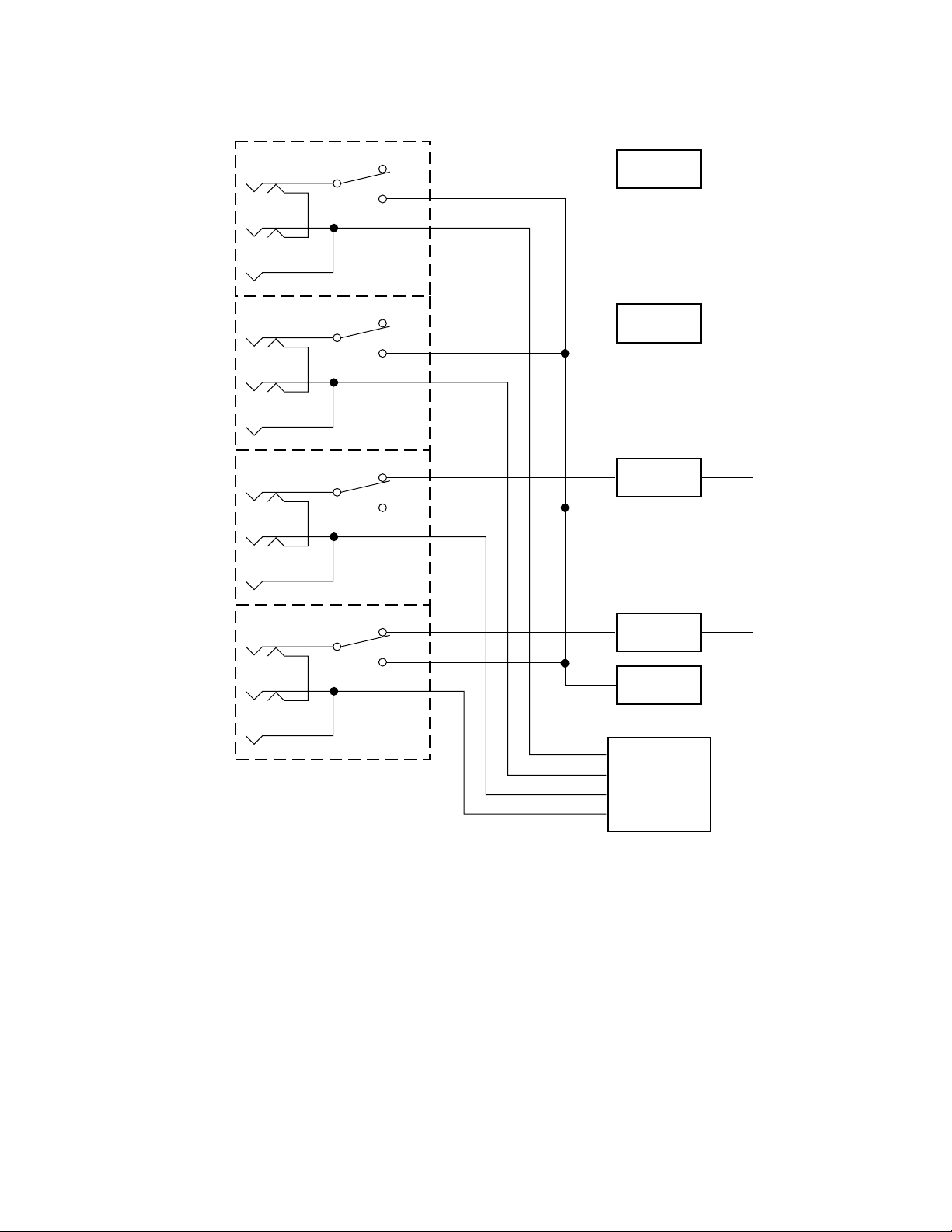
The PS chassis is the stan dard EI A 19-in ch rack moun ted uni t wit h a ba ckplane and s pace f or 18
modules. The early chassis (PSC-01 and PSC-02) can be identified by the six pin in-line power
connector located on the back upper left corner of the chassis. The later chassis (RDC-01 and
RDC-02) can be identified by the nine pin square power connector located on the back upper
left corner of the chassis.
The RDC-01/02 backplane consists of a printed circuit board assembly with eighteen 96-pin
connectors on the inside of the card cage and 50 D-subminiature (DB) 25-pin connectors, two
(DB) 9-pin connectors , one 20-pin dual in-lin e (DI N ) con nector and one 9-pin squar e co nnector
on the back of the board.
2.2.2 PatchSwitch Control Module (RDM-15B)
Manual operation of the PatchSwitch Control Module switches provides local control of the
switch and alarm functions. The Control Module is microprocessor-based and provides the
interfacing cap abilities for b oth m anua l, dc pulse bank swit ching and remote cont rol operations.
A four-position DIP switch on the Control Module encodes the chassis identification number.
Remote control devices use this number to select the PS chassis (see Table 6-1). The Control
Module is located in position 18 (slot 18) of all PatchSwitch chassis.
Page 1-6
© 1999, ADC Telecommunications, Inc.
Page 17

ADCP-50-304 • Issue 19 • June 199 9 • Sec tion 1: In troduction
2.2.3 Data Converter Module (PSR-06)
This module is a printed circuit board assembly with components, a front panel with four LED
status indicators and a rear 96-pin DIN connector. The module interfaces with the ADC Remote
Control Unit, a user's CRT terminal, or computer, and converts signals providing RS-422/RS232 compatib ility to permit remote s erial control for PatchSwitch equipm ent to be co nnected to
RS-232 modem or CRTs.
2.2.4 LED/Alarm Patch Module with A/B Switching (PSM-01)
This PS module is a printed circuit board assembly with components, a front panel (two toggle,
one rotary and one touch switch, three patch 26-pin connectors, and 11 LEDs), and rear 96-pin
DIN connector. It may be mounted in any of the first 16 module positions.
2.2.5 Patch Module with A/B Switching (PSM-02)
This PS module has the same features as PSM-01 except without RS-232/V.24 lead status
indicators and alarming.
2.2.6 A/B Switching Module (PSM-03)
This PS module is a printed circuit board assembly with components, a front panel (one toggle
switch and two LEDs) and a rea r 96-pin DIN conne ctor. It may be mounted in any of the first 16
module positions.
2.2.7 Led/Alarm Patch Module with A/B Switching and Off-Line Access (PSM-04)
This module is the same as PSM-01 except that when it is in A or B state, the off-line port
provides direct test access to the off-line device.
2.2.8 Patch Module with A/B Switching and Off-Line Access (PSM-05)
Same as PSM-04 except this module has no LEDs or alarm.
2.2.9 LED/Alarm Patch Interface (PSM-07)
This module (normally mounted in the 17th position of the chassis but may be mounted in the
1st through 16th position) is a patch interface module with LED and alarm; the model is a
printed circuit board assembly with components, a front panel (one toggle, one rotary and one
touch switch, two patch 26-pin connectors and nine LEDs), and a rear 96-pin DIN connector.
2.2.10 Patch Interface (PSM-08)
This module (normally mounted in the 17th position of the chassis but may be mounted in the
1st through 16th position) is a patch interface module; the module is a printed circuit board
assembly with a front panel (two patch 26-pin connectors) and rear 96-pin connector.
© 1999, ADC Telecommunications, Inc.
Page 1-7
Page 18

ADCP-50-304 • Issue 19 • June 1999 • Section 1: Introduction
2.2.11 Blank Panel (PSM-09)
This panel is used in chassis module positions in lieu of a module. The panel is a two piece
assembly secured to the chassis by two mounting screws.
2.2.12 Test Module (PSM-12)
Test Module PSM-12 is normally mounted in the slot position 17 of the PS chassis, but may be
mounted in any slot to the left of position 17 (1 through 16). This module provide the user with
RS-232/V.24 interface capabilities and status monitoring for eight (8) leads and alarm
conditions. The module contains three female RS-232/V.24 ports (one on the front panel and
two on the rear of the module) and a patch jack. All four connectors are hardwired in parallel.
The eight RS-232/V.24 leads monitored for status include: TD; RD; DCD; SQ; RTS; CTS;
DSR; and DTR. Each lead contains an associated LED indicator, located on the front panel,
which turns on when the signal is active (or high). An adjustable alarm circuit with associated
LED (ALM) is also provided to inform the user when a preselected alarm condition exits. After
an alarm conditions occurs, the alarm circuit may be reset by the operator touching the finger
reset (RST) switch. A toggle switch is also provided to enable/disable the alarm LED.
2.2.13 Test Module (PSM-13)
Test Module PSM-13 is normally mounted in slot 17 of the PS chassis, but may be mounted in
any slot to the left of position 17 (1 through 16). This module provides the user with interface
capabilities to spare devices or test equipment. The front panel of the Test Module contains one
female DB25 port and one patch jack. The rear of the module at slot position 17 contains two
female RS-232/V.24 ports. All four connectors are hardwired in parallel.
2.2.14 PatchSwitch Chassis AC Power Supply (PSW-000001)
This power supply is a plug-in unit used when the power source is from 90 to 240 Vac, 48-63
Hz. This power s uppl y has a six pin in-line c onne ct or f or use wi th chassis PSC-01 and PSC-02.
2.2.15 PatchSwitch Chassis AC Power Supply (PSW-000003)
This power supply is a plug-in unit used when the power supply source is from 90 to 240 Vac,
48-63 Hz. This power supply has a nine pin square connector for use with chassis RDC-01 and
RDC-02.
2.2.16 Standard Patch Cords (PMPC-X)
The standard patch cords used with the PC chassis modules are described in Table 1-2.
Page 1-8
© 1999, ADC Telecommunications, Inc.
Page 19

3 SPECIFICATIONS
Physical Character is ti cs
PS Chassis
Environmental Conditions
Ambient Temperature:
Relative Humidity:
Power Requirements
PS Chassis:
ADCP-50-304 • Issue 19 • June 199 9 • Sec tion 1: In troduction
Height: 7 inches (17.78 cm)
Width: 19 inches (48.3 cm)
Depth: 12 inches (30.12 cm)
Operating: +32° F to +122° F (0° C to +50° C)
Storage: –40° F to +158° F (–40° C to +70° C)
Operating:10% to 80% noncondensing
Storage: 5% to 90% noncondensing
+5 Vdc @ 3 amps
+12 Vdc @ 1 amp (switching)
3.1 DMPS-10 AC Power Supply
The DMPS-10 AC Power Supply provides all dc operating voltages and current required by up to
four fully-populated RDC-01 or RDC-02 chassis. The rack mounted power supply plugs directly
into a standard 110 Vac primary power source outlet. This power supply can also be set for use
with 240 Vac. The power supply comes equipped with one nine-conductor power cord and an AC
line cord. The DMPS-10 will power one PS assembly and can house up to three additional
DMPS-10 EXP expansion power modules to supply power for four PS chassis assemblies.
© 1999, ADC Telecommunications, Inc.
Page 1-9
Page 20

DESCRIPTION
FUNCTIONAL
Page 21

SECTION 2: FUNCTIONAL DESCRIPTION
Content Page
1 GENERAL. . . . . . . . . . . . . . . . . . . . . . . . . . . . . . . . . . . . . . . . . . . . . . . . . . . . . . . . . . . . . . . . . . . . . . . . . . . .2-1
2 PATCHING WITH IN-LINE A/B SWITCHING . . . . . . . . . . . . . . . . . . . . . . . . . . . . . . . . . . . . . . . . . . . . . . . . . . . . . .2-1
3 A/B SWITCHING WITH OFF-LINE MONITOR ACCESS. . . . . . . . . . . . . . . . . . . . . . . . . . . . . . . . . . . . . . . . . . . . . . .2-2
3.1 PS Control Module (RDM-15) . . . . . . . . . . . . . . . . . . . . . . . . . . . . . . . . . . . . . . . . . . . . . . . . . . . . . . . .2-3
3.2 LED/Alarm Patch M odule with A/B Switching and In- Line Patch Access (PSM-01). . . . . . . . . . . . . . . . . . . . .2-7
3.3 Patch Module with A/ B Swit ching and In-Line Patch Acc es s (PSM -02) . . . . . . . . . . . . . . . . . . . . . . . . . . .2-11
4 A/B SWITCHING MODULE (PSM -0 3). . . . . . . . . . . . . . . . . . . . . . . . . . . . . . . . . . . . . . . . . . . . . . . . . . . . . . . . .2-12
5 LED/ALARM PATCH MODULE WITH A/B SWITCHING AND OFF-LINE ACCESS (PSM-04) . . . . . . . . . . . . . . . . . . . . . .2-13
6 PATCH MODULE WITH A/B SWITCHING AND OFF-LINE ACCESS (PSM-05) . . . . . . . . . . . . . . . . . . . . . . . . . . . . . . .2-13
7 LED/ALARM PATCH INTERFACE (PSM-07). . . . . . . . . . . . . . . . . . . . . . . . . . . . . . . . . . . . . . . . . . . . . . . . . . . . .2-13
7.1 Patch Interface (PSM -08) . . . . . . . . . . . . . . . . . . . . . . . . . . . . . . . . . . . . . . . . . . . . . . . . . . . . . . . . . .2-14
8 TEST MODULE (PSM-12) . . . . . . . . . . . . . . . . . . . . . . . . . . . . . . . . . . . . . . . . . . . . . . . . . . . . . . . . . . . . . . . .2-15
9 TEST MODULE (PSM 13) . . . . . . . . . . . . . . . . . . . . . . . . . . . . . . . . . . . . . . . . . . . . . . . . . . . . . . . . . . . . . . . .2-16
10 PS RS-422/RS-232 INTER FACE CONVERTER MOD ULE (PSR-06). . . . . . . . . . . . . . . . . . . . . . . . . . . . . . . . . . . . . .2-17
11 PS CHASSIS POWER . . . . . . . . . . . . . . . . . . . . . . . . . . . . . . . . . . . . . . . . . . . . . . . . . . . . . . . . . . . . . . . . . . . 2-18
_________________ ___________________ ______________________________________ _______________________________
ADCP-50-304 • Issue 19 • June 1999 • Se ct ion 2: Fun ct i ona l Description
1 GENERAL
This section describes how the PatchSwitch equipment functionally operates in a data
communications netw ork. The PS equipment pro vide s two main f uncti ons. A user selec ts one o f
two DTE data cha nnel s to connect to a DCE. Add it ion al ly, the user can monitor an d r es tor e dat a
channels with a manual patch.
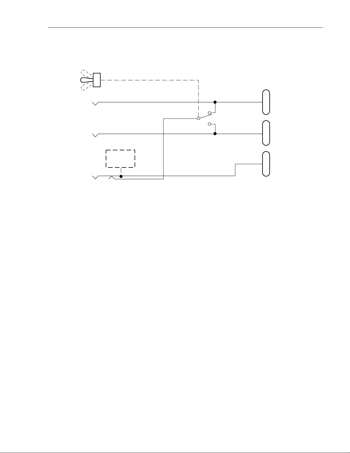
2 PATCHING WITH IN-LINE A/B SWITCHING
A functiona l diagram illustrati ng patching wi th in-line A/B swit ching is shown in Figure 2-1.
Computer access is through the COMPUTER patch cord jack and either the DTE-A or DTE-B
jack. Modem connection is through the MODEM patch cord jack and the DCE jack. Monitor
connection is through the MONITOR patch cord jack.
© 1999, ADC Telecommunications, Inc.
Page 2-1
Page 22
ADCP-50-304 • Issue 19 • June 1999 • Section 2: Functional Description
FRONT PANEL
CONNECTIONS
COMPUTER
MODEM
MONITOR
LED/ALARM
ELECTRONICS
(PSM-01
ONLY)
Figure 2-1. PatchSwitch with In-Line Access (PSM-01, PSM-02)
BACKPLANE
CONNECTIONS
A
B
J1 DTE-A
J2 DTE-B
J3 DCE
1607-A
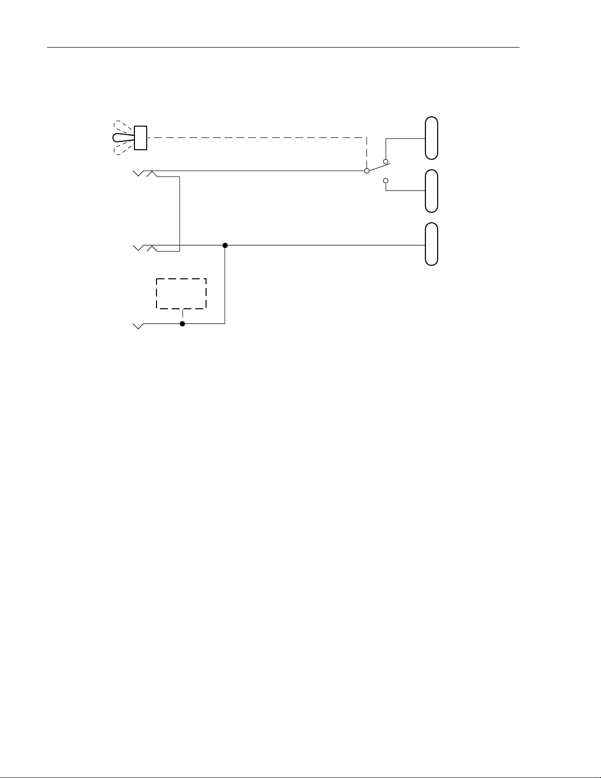
3 A/B SWITCHING WITH OFF-LINE MONITOR ACCESS
The capability for accessing the off-line DTE device is illustrated in Figure 2-2. The upper port
(A) provides patch cord access to the upper “D” subminiature connector (J-1) on the chassis
rear panel. When the module is in the “A” or normal state, this provides a monitor function. If
the module is in the “B” or “sub” state, this provides direct test access to the off-line device.
The middle port (B) functions in the same manner for the middle connector (J-2) on the chassis
backplane; “B” state, monitor access. “A” state, test access to the off-line “B” device.
The lower port (C) provides “intrusive” test access to the lower (J-3) connector on the chassis
backplane. Insertion of a patch cord in this port, regardless of switch status, breaks the circuit
and connects the patch cord to the common (DCE) device.
Page 2-2
© 1999, ADC Telecommunications, Inc.
Page 23
FRONT PANEL
CONNECTIONS
A
B
ADCP-50-304 • Issue 19 • June 1999 • Se ct ion 2: Fun ct i ona l Description
BACKPLANE
CONNECTIONS
A
B
LED/ALARM
ELECTRONICS
(PSM-04
ONLY)
C
Figure 2-2. PatchSwitch with Off-Line Access (PSM-04, PSM-05)
3.1 PS Control Module (RDM-15)
The PS Contro l Mod ule (C M) c ontro ls the overall manu al o pera tions of th e mod ules cont ained
in the PS chassis. Three toggle switche s l oca ted on the front panel have the fo ll owing functi ons:
1. Bank switch all PS modules to either the “A” or “B” position. That is, switch all modules
at the same time to either the “A” position or “B” position.
A
B
J1 DTE-A
J2 DTE-B
J3 DCE
1608-A
2. Enable the bank switch and the individual module A/B switches.
3. Reset all of the modules' alarm circuits.
The audible alarm circuitry is in the CM. It activates when an individual PS module detects an
alarm condition (according to the alarm selection configuration on the module). Alarm
conditions are detected only by modules which contain circuitry. The alarm circuitry must also
be conditioned by proper strapping (jumper) of the individual PS chassis module.
When the alarm conditi on occurs, the individual module energizes it s ye ll ow LED indicator and
the CM audible alarm sounds. The operator toggles the reset switch to reset the alarm circuitry.
The PS Control Module is equipped with a selectable remote control feature. Depending on the
strap position the CM will either accept serial RS-422 or dc level (pulse) signals through the 9pin D-subminiature connector. The CM is shipped strapped for RS-422 control.
With the CM strapped for serial RS-422 remote control, the CM provides an interface between
the PS chassis modules and a remote control device (see Figure 2-3 and Figure 2-4). The
following devices can be used for remote control of a PS chassis.
1. PatchSwitch Remote Control Unit (RCU, PSR-03) (See ADCP-50-302 User Manual.)
2. Terminal or computer (asynchronous ASCII device).
© 1999, ADC Telecommunications, Inc.
Page 2-3
Page 24
ADCP-50-304 • Issue 19 • June 1999 • Section 2: Functional Description
A remote control device can control the operation of up to 16 full PS chassis assemblies (16
modules each) using a dedicated communications channel. This channel has four signals:
1. Transmit Data (TD)
2. Receive Data (RD)
3. Clear-To-Send (CTS)
4. Request-To-Send (CTS)
Each of the abo ve signals ha s t he same function as th e corresponding sig nal s defined by the RS232 standard.
The communications channel transmission medium is a cable consisting of four twisted wires
within an overall shield. The shield is ground potential.
Note:
The electrical characteristics of the communications channel cable (9-wire)
conform to RS-422A/V.11 (X.27) standards.
COMMUNICATIONS
CHANNEL**
MASTER A/B
ENABLE
RESET
REMOTE
CONTROL DEVICE
CONTROL
MODULE*
SLOT 18
* STANDARD
CONTROL OR
REMOTE
CONTROL
** USED ONLY
BY REMOTE
CONTROL
MODULE
P/S
C
H
A
S
S
S
B
A
C
K
P
L
A
N
E
TO NEXT P/S CHASSIS
MODULE 0
SLOT 1
MODULE 1
I
SLOT 2
P/S MODULES
2 THROUGH 14
(SLOT 3-15)
MODULE 15
SLOT 16
SLOT 17
1609-A
Figure 2-3. Control Module, Simplified Block Diagram (Standard and Remote)
Page 2-4
© 1999, ADC Telecommunications, Inc.
Page 25
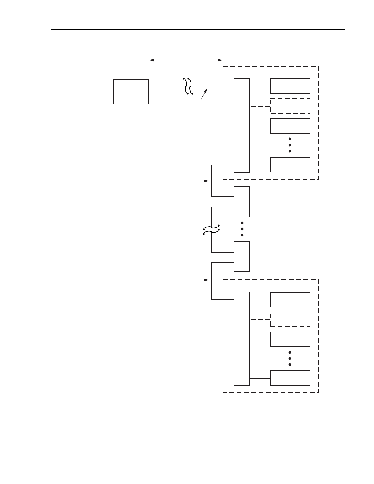
UP TO 1000 FT.
(304 M)
ADCP-50-304 • Issue 19 • June 1999 • Se ct ion 2: Fun ct i ona l Description
PATCHSWITCH CHASSIS 0
REMOTE
CONTROL
UNIT
RS-422
RS-232
COMMUNICATION
RS-422
COMMUNICATION
CHANNEL
RS-422
CHANNEL
B
A
C
K
P
L
A
N
E
PS CHASSIS 1
PS CHASSIS 6
CM 0
SLOT 18
SLOT 17
PS MODULE
SLOT 16
SLOTS
2 – 15
PS MODULE
SLOT 1
PS CHASSIS
2 – 5
RS-422
COMMUNICATION
CHANNEL
PATCHSWITCH CHASSIS 7
B
A
C
K
P
L
A
N
E
SLOTS
2 – 15
CM 7
SLOT 18
SLOT 17
PS MODULE
SLOT 16
PS MODULE
SLOT 1
1610-A
Figure 2-4. RCU to Local PatchSwtich Chassis, Interconnection Block Diagram
© 1999, ADC Telecommunications, Inc.
Page 2-5
Page 26

ADCP-50-304 • Issue 19 • June 1999 • Section 2: Functional Description
The cable connectors are 9-pin, D-subminiature. Both end-connectors are male. The cable may
be up to 1,000 feet in length. Connector pin assignments are detailed in Table 2-1.
Table 2-1. Communications Channel Connector Pin Assignments
SIGNAL NAME PIN NUMBER DIRECTION OF SIGNAL
TD +
TD –
6
7
Input
Input
RD +
RD –
CTS +
CTS –
RT S +
RT S –
GRD – 1Ground
2
3
4
5
8
9
Output
Output
Output
Output
Input
Input
Each PS chassis contains two female 9-pin D-subminiature connectors wired in parallel. A
cable connects one PS chassis to another in daisy-chain fashion. A long cable connects the
remote contro l device to the first (or last) P S chassis i n the chai n. Up to 16 PS chass is may be
interconnected via the communications cable to a remote control device.
All transmissions between the PatchSwitch Control Module and the remote control device must
use the ASCII character set. The PS chassis is a DCE device and has the following data
transmission characteristics:
1. Speed of 1200 bits per second
2. Asynchronous transmission
3. Bit-serial ASCII data (8 bit no parity)
4. One Stop bit.
During normal operations, only one (of the possible 16) PS chassis CM may transmit on the
communications channel at one time. When a PS Chassis is selected by the remote control
device, all other PS chassis connected on the same channel are disabled (de-selected). All
manual controls on a CM are always functional.
With the CM strapped for dc pulse control, the CM provides capability to bank switch PS chassis
modules by application of 0V (GND), +5V or –5 V to –48V dc voltage levels on the 9- pin Dsubminiature connector. The connector pin assignments are detailed in Table 2-2.
Page 2-6
© 1999, ADC Telecommunications, Inc.
Page 27

ADCP-50-304 • Issue 19 • June 1999 • Se ct ion 2: Fun ct i ona l Description
Table 2-2. DB-9 Pinout and Signal Characteristics
PIN OULTAGE INPUT CHANNEL (SWITCHED TO)
1 Chassis Ground N/A
2 –48V +5% (–5V min) B
3+5V +5% B
4 Remote Ground In B
5 Signal Return N/A
6 –48V +5% (–5V min) A
75V +5% A
8 Remote Ground In A
9 Signal Return N/A
The dc voltages indicated in Table 2-2 must be present for a minimum of 250 msec
Note:
to ensure switching.
Up to four (4) PS chassis can be bank switched by daisy chaining the CMs via the 9-pin Dsubminiature and ensuring that each CM is strapped for dc pulse control.
The CM is also equipped with a selectable Autofallback feature. When an alarm condition is
detected, automatic switching is performed between the “A” and “B” sides of the PS modules.
The “A” to “B” side, or “B” to “A” automatic switching operation is selected by installing a
jumper on the CM circuit board. After configuring the Autofallback option, the PS module
detecting the alarm swi tc hes to t he designated side (dep endi ng on the strap install ed) , it re mains
in the switched position regardless of subsequent alarm status.
Alarm indications are automatically reset after the module detecting the alarm switches to the
appropriate side if the module is strapped for “Automatic Reset” (recommended). When the
front panel alarm (
ALM
) selection is posi ti one d in the
OFF
position, the autof al lback feature is
disabled for that module.
3.2 LED/Alarm Patch Module with A/B Switching and In-Line Patch Access (PSM-01)
This PS module provides patching and switching functions together with lead status, switch
status, and alarm indications. A simplified circuit of this module is shown in Figure 2-5.
The A/B switch activates relays to connect the computer patch cord jack either the DTE-A port
or the DTE-B port. The indicators show A/B switch position, alarm and RS-232 lead status.
Figure 2-6 shows a more detailed diagram of the module. In addition to switching between
DTE-A or DTE-B, th e rel ay s als o swit ch in th e int er lo ck ju mp er. Interlockin g is use d to pro te ct
the user from accidentally switching a common backup piece of equipment onto two or more
different data lines. This is accomplished by allowing only the first module in that group to
switch. The remaining modules r emain in the “no rmal sta te” or the “A” position. Modules in the
“B” position once switched to “A” will remain in the “A” position.
© 1999, ADC Telecommunications, Inc.
Page 2-7
Page 28

ADCP-50-304 • Issue 19 • June 1999 • Section 2: Functional Description
The three classes of interlock groups available are:
1. Global Interlock: Groups 1 and 2 are global and may be extended to all chassis in a
system, using a 20-p in i nt er cha ssi s i nt er loc k cable. W it h t hi s gr ouping, all modules having
a jumper placed on group 1 make up one group, and all modules with a ju mp er on gr oup 2
make up the other group. Interchassis interlock cables must be installed between chassis.
Each module interlock group may have no more than one jumper installed at a time.
2. Horizontal Interlock: Groups 3 and 4 are horizontal and they include only modules in the
individual chassis. With this grouping, all modules having a jumper placed on group 3
make up one group, and all modules with a jumper on group 4 make up the other group.
These groupings do not extend out of the chassis and are not affected by the interchassis
interlock cable. Each module interlock group jumper block may have no more than one
jumper installed at a time.
3. Vertical Interlock: The vertical in terl ock ju mper po siti on is la beled V. Placi ng a jump er in
this position interlocks all modules in the same slot location in other chassis having a
jumper install ed on the same V position . Interchassis interlo ck cables must be installe d
between chassis. The interchassis interlock cable is a 20 position ribbon cable (4WC-03)
with a 20-pin connector for each chassis. Each module interlock group jumper block may
have no more than one jumper installed at a time.
LEDs show the status of eight RS-232 leads. Each lead has a jumper connection to the alarm
circuit control logic. The alarm is thus user selectable for any of eight leads. The EIA RS-232/
CCITT V.2 4 modem interface signal l eads are shown in Table 2-3. The al arm circuit control
logic supplies the alarm signal to the control module and an alarm indicator. This logic is also
controlled by the RST (Reset) touch switch, toggle switch OFF (LED off, audible alarm off),
ALM (LED and audible alarm on) and LED (LED on, audible alarm off), and rotary switch
DLY (alarm time delay setting). The alarm may be automatically reset if the automatic alarm
reset jumper is in place. LED status indicators with their color and signal definition is shown in
Table 2-4. Table 2-5 shows the alarm delay settings.
Caution: The bank switching feature is not compatible with the group interlock feature. If no
module in an interlocked group is in the B state when a bank switch to the B state is initiated,
only the first module in this group will switch to the B state. Data may be lost when more than
one module is in the B state of an interlocked group. If one module in an interlocked group is in
the B state when a bank switch is initiated, the rest of the modules in that interlocked group do
not switch to the B state; consequently, the system maintains its integrity
.
Page 2-8
© 1999, ADC Telecommunications, Inc.
Page 29
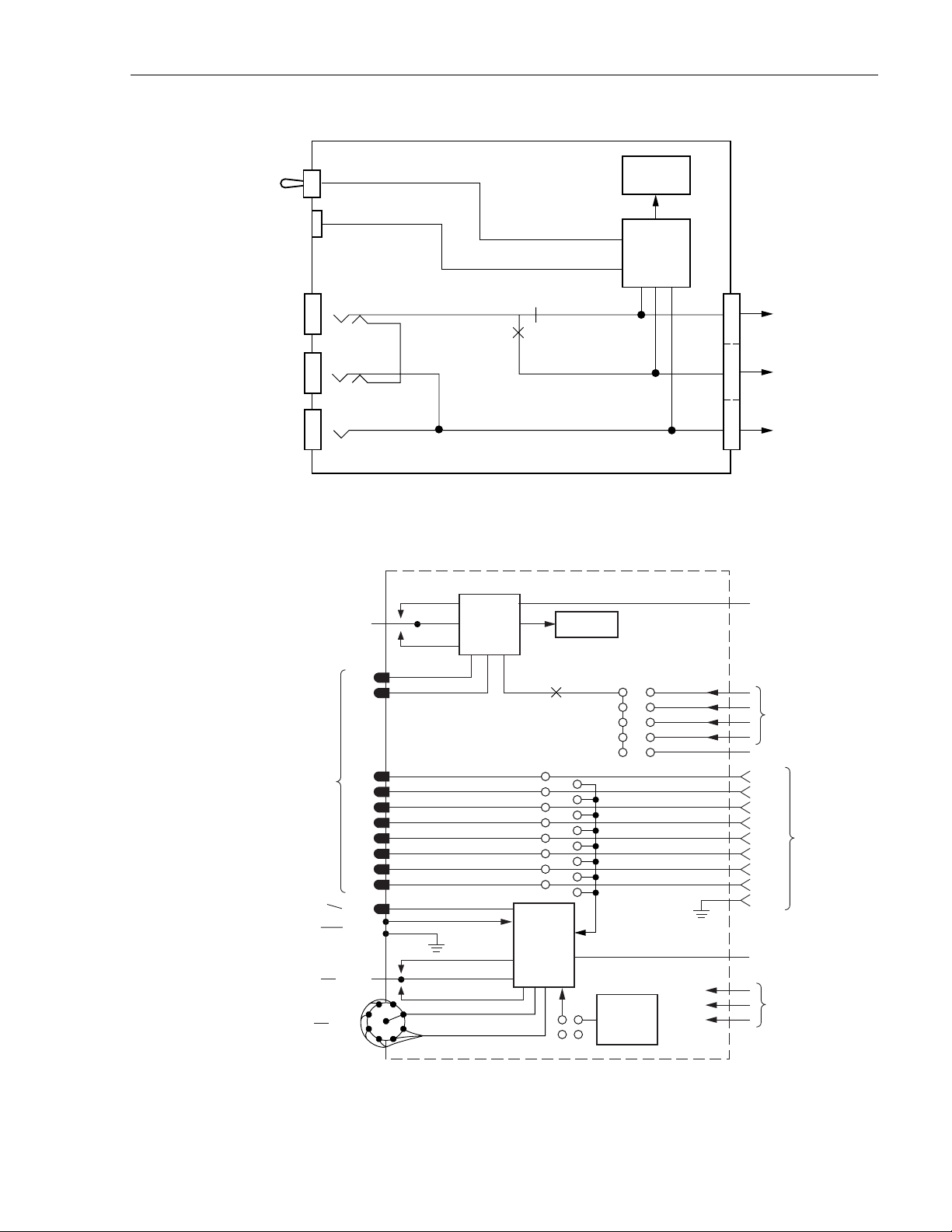
ADCP-50-304 • Issue 19 • June 1999 • Se ct ion 2: Fun ct i ona l Description
A/B
SWITCH
1641-A
INDICATORS
COMPUTER
MODEM
MONITOR
A/B
RELAY
A/B
RELAYS
A/B
DTE AND
ALARM
LOGIC
DTE
(A)
DTE
(B)
DCE
UPPER
INTERFACE
PORT
LOWER
INTERFACE
PORT
Figure 2-5. LED/Alarm Patch Module with A/B Switchin g Simplified Circuit Diagram
STATUS
INDICATORS
ALARM
INDICAT OR
TOUCH
SWITCH
TOGGLE
SWITCH
ROTARY
SWITCH
TOGGLE
SWITCH
ALM
DL Y
TD
RD
DCD
SQ
RTS
CTS
DSR
DTR
ALM
RST
A
B
OFF
LED
A
B
A/B
SWITCH
LOGIC
A/B SWITCH CONTROL
A/B
RELAYS
INTERLOCK
A/B
RELAYS
ALARM
JUMPER
ALARM
CIRCUIT
CONTROL
LOGIC
AUTOMA TIC
ALARM
RESET
STORE
A/B
JUMPER
GROUP 1
2
3
4
V
ALARM
+5 Vcd
GND
+12 Vcd
1611-A
CONTROL
MODULE
PIN 2
PIN 3
PIN 8
PIN 21
PIN 4
PIN 5
PIN 6
PIN 20
PIN 7
CONTROL
MODULE
BACKPLANE
RS-232
LEADS
BACKPLANE
Figure 2-6. LED/Alarm Patch Module with A/B Switching Detailed Circuit Diagram
© 1999, ADC Telecommunications, Inc.
Page 2-9
Page 30

ADCP-50-304 • Issue 19 • June 1999 • Section 2: Functional Description
Table 2-3. RS-232 Modem Terminal Interface
PIN NAME SOURCE FUNCTION CIRCUIT CCITT/EIA
1* FG — Frame Ground 101 (AA)
2* TD DTE Transmitted Data 103 (BA)
3* RD DCE Received Data 104 (BB)
4* RTS DTE Request To Send 105 (CA)
5* CTS DCE Clear To Send 106 (CB)
6* DSR DCE Data Set Ready 107 (CC)
7* SG — Signal Ground 102 (AB)
8* DCD DCE Data Carrier Detect 109 (BA)
9* DCE Positive DC Test Voltage
10* DCE Negative DC Test Voltage
11*
12* SRLSD DCE Sec Data Carrier Detect 122 (SCF)
13* (S)CTS DCE Sec Clear To Send 121 (SCB)
14* STD DTE Sec Transmittal Data 128 (SBA)
15* TC DCE Transmitter Clock 114 (DB)
16* SRD DCE Sec Received Data 119 (SBB)
17* RC DCE Receiver Clock 115 (DD)
18*
LL DTE Local Loopback 141 (LL)
19* SRTS DTE See Request To Send 120 (SCA)
20* DTR DTE Data Terminal Ready 108/2 (CD)
21* SQ DCE Signal Quality Detect 110 (CG)
22* RI DCE Ring Indicator 125 (CE)
23* DTE Data Rate Selector 111 (CH)
Data Rate Selector 112 (CI)
24* ETC DTE Ext Transmitter Clock 113 (DA)
25* TM DCE Test Mode 142 (TM)
Page 2-10
© 1999, ADC Telecommunications, Inc.
Page 31

ADCP-50-304 • Issue 19 • June 1999 • Se ct ion 2: Fun ct i ona l Description
Table 2-4. LED Status Indicators
LED STATUS INDICATOR COLOR SIGNAL DEFINITION
A Red DTE-A
B Green DTE-B
TD Green Transmitted Data
RD Green Received Data
DCD Green Data Carrier Detect
SQ Green Signal Quality Detect
RTS Red Request To Send
CTS Red Clear To Send
DSR Red Data Set Ready
DTR Red Data Terminal Ready
ALM Yellow Alarm On
Table 2-5. Alarm Time Delay Settings
TIME DELAY
ARC LENGTH 50 HZ AND 60 HZ ENVIRONMENT
γ
1 µsec
Shortest 64 msec
256 msec
0.51 sec
1.02 sec
8.19 sec
32.75 sec
Longest 65.5 sec
3.3 Patch Module with A/B Switching and In-Line Patch Access (PSM-02)
This PS module operates similarly to the PSM-01 by providing patching, switching, and switch
status indicatio n, e xcept it does no t cont ain LED statu s indi cator s and alar m ci rcuitry. A detailed
circuit diagram of this module is shown in Figure 2-7.
© 1999, ADC Telecommunications, Inc.
Page 2-11
Page 32

ADCP-50-304 • Issue 19 • June 1999 • Section 2: Functional Description
4 A/B SWITCHING MODULE (PSM-03)
This module provides A/B swit ching only. A simplified circuit diagr am of t his module is show n
in Figure 2-8.
The A/B switch activates the A/B relays. The A/B relays complete the channel between the DCE
and either DTE-A or DTE-B. The re lays also switc h in the interl ock jumper. Interlocking from
the control mod ule protects the user fr om accidentally switchin g common backup equip ment
onto two or more different data lines. The thre e classes of interlo ck groups available are:
1. Global Interlock: Groups 1 and 2 are global and may be extended to all chassis in a
system, using a 20-p in i nt er cha ssi s i nt er loc k cable. W it h t hi s gr ouping, all modules having
a jumper placed on group 1 make up one group, and all modules with a ju mp er on gr oup 2
make up the other group. Interchassis interlock cables must be installed between chassis.
Each module interlock group may have no more than one jumper installed at one time.
2. Horizontal Interlock: Groups 3 and 4 are horizontal and they include only modules in the
individual chassis. With this grouping, all modules having a jumper placed on group 3
make up one group and all modules with a jumper on group 4 make up the other group.
These groupings do not extend out of the chassis and are not affected by the interchassis
interlock cable. Each module interlock group jumper block may have no more than one
jumper installed at a time.
3. Vertical Interlock: The vertical in terl ock ju mper po siti on is la beled V. Placi ng a jump er in
this position interlocks all modules in the same slot location in other chassis having a
jumper instal led on the came V position. Interch assis interlock c ables must be inst alled
between chassis. The interchassis interlock cable is a 20 position ribbon cable (4WC-03)
with a 20-pin connector for each chassis. Each module interlock group jumper block may
have no more than one jumper installed at a time.
TOGGLE
SWITCH
INDICATORS
A
B
A
B
Figure 2-7. Patch Module with A/B Switching Detailed Circuit Diagram
A/B
SWITCH
LOGIC
A/B
REPLAYS
A/B
REPLAYS
ALARM
A/B
INTERLOCK
JUMPER
GROUP 1
2
3
4
V
1612-A
BACKPLANE
Page 2-12
© 1999, ADC Telecommunications, Inc.
Page 33

ADCP-50-304 • Issue 19 • June 1999 • Se ct ion 2: Fun ct i ona l Description
TOGGLE
SWITCH
A/B SWITCH CONTROL
A
B
A
B
A/B
SWITCH
LOGIC
A/B
RELAYS
A/B
RELAY
A/B
RELAYS
A/B
INTERLOCK
JUMPER
GROUP 1
2
3
4
V
VERTICAL
INTERLOCK
1613-A
CONTROL
MODULE
TO CHASSIS
BACKPLANE
DTE
(A)
DTE
(B)
DCE
UPPER
INTERFACE
PORT
LOWER
INTERFACE
PORT
Figure 2-8. A/B Switching Module Simplified Circuit Diagram
5 LED/ALARM PATCH MODULE WITH A/B SWITCHING AND OFF-LINE ACCESS (PSM-04)
This module i s the same as PSM-01 except that when it is in the A/B state, the o ff-line port
provides direct test access to the off-line device (see Figure 2-2).
6 PATCH MODULE WITH A/B SWITCHING AND OFF-LINE ACCESS (PSM-05)
This module is the same as PSM-04 except it does not have LEDs or Alarm.
7 LED/ALARM PATCH INTERFACE (PSM-07)
This PS module provides interface patching together with status and alarm indications. A
simplified circuit illustrating patching only is shown in Figure 2-9.
The COMPUTER patch cord jack connects directly to the chassis rear upper interface port. The
MONITOR patch cord jack connects directly to the chassis rear lower interface port. The
monitoring and alar m ci rcuits of the PS mod ule are show n in Figure 2-10. LEDs s how the statu s
of eight RS-232 leads. Each lea d has a j umper conne ct ion to the alarm circuit cont ro l lo gic. The
© 1999, ADC Telecommunications, Inc.
Page 2-13
Page 34

ADCP-50-304 • Issue 19 • June 1999 • Section 2: Functional Description
alarm is thus user select able for any one of eight leads of th e lo wer patch por t. The EIA RS-232 /
CCITT V.2 4 modem interface signal l eads are shown in Table 2-3. The al arm circuit control
logic supplies the alarm signal to the control module and an alarm indicator. This logic is also
controlled by the RST (Reset) touch switch, toggle switch OFF (LED off, audible alarm off),
ALM (LED and audible alarm on), LED (LED on, audible alarm off), and rotary switch DLY
(alarm time delay setting). The alarm may be automatically reset if the automatic alarm reset
jumper is in place. LED status indicators with their color and signal definition are shown in
Table 2-4. Alarm delay settings are shown in Table 2-5.
7.1 Patch Interface (PSM-08)
This PS module provides interface patching. A simplified circuit showing patching is shown in
Figure 2-9.
The COMPUTER patch cord jack connects directly to the chassis rear upper interface port. The
MONITOR patch cord jack connects directly to the chassis rear lower interface port.
COMPUTER
MONITOR
UPPER
INTERFACE
PORT
LOWER
INTERFACE
PORT
1614-A
Figure 2-9. Patch Interface Simplified Circuit Diagram
Page 2-14
© 1999, ADC Telecommunications, Inc.
Page 35

ADCP-50-304 • Issue 19 • June 1999 • Se ct ion 2: Fun ct i ona l Description
TOGGLE
SWITCH
TD
RD
DCD
SQ
RTS
CTS
DSR
DTR
ALM
ALM
RST
BACKPLANE
ALARM
JUMPER
STATUS
INDICATORS
PIN 2
PIN 3
PIN 8
PIN 21
PIN 4
PIN 5
PIN 6
PIN 7
PIN 20
LOWER
INTERFACE
RS-232C
LEADS
ALARM
CONTROL
MODULE
+5 Vcd
GND
STORE
AUTOMATIC
ALARM
RESET
ALARM
CIRCUIT
CONTROL
LOGIC
OFF
LED
DL Y
ROTAR Y
SWITCH
TOUCH
SWITCH
ALARM
INDICAT OR
1615-A
8 TEST MODULE (PSM-12)
Test Module PSM-12 provides the user with RS-232/V.24 interface capabilities, status
indicators for eight (8) leads and alarm conditions. A simplified block diagram illustrating the
test module connections is shown in Figure 2-11. Two female RS-232/V.24 TEST ports, located
on the rear of the test module, are available for connecting the test equipment. Another female
RS-232/V.24 port and a patch jack are located on the module front panel. All four connectors
are hardwi red in paral lel.
The eight RS-232/V.24 circuit leads having LED indicators are: TD; RD; DCD; SQ; RTS; CTS;
DSR; and DTR. When a monitored circuit lead is active (signal present), the associated LED
indicator turns on (only while the signal is present). The colors and signal definitions for the
applicable LED status indicators are detailed in Table 2-4.
An adjustable alarm circuit with associated LED (ALM), is provided to inform the user when a
preselected alarm condition exists on one of the monitored leads. Each monitored lead has a
jumper connection to the alarm circuit control logic. The alarm is user selectable for any one of
the eight leads. The RS-232/V.24 interface signal leads are defined in Tab le 2- 3. The alarm
circuit control logic supplies the alarm signal to the control unit and an alarm indicator.
Figure 2-10. LED/Alarm Patch Interface Detailed Circuit Diagram
Except for th e A/B switching circuits, the circ uit diagram shown in Figu re 2-6 is
Note:
applicable to PSM-12.
© 1999, ADC Telecommunications, Inc.
Page 2-15
Page 36

ADCP-50-304 • Issue 19 • June 1999 • Section 2: Functional Description
This logic is also controlled by the RST (Reset) touch switch, toggle switch OFF (LED off,
audible alarm off), ALM (LED and audible alarm on), LED (LED on, audible alarm off), and
rotary switch DLY (alarm time delay setting). The alarm may be automatically reset if the
automatic alarm reset jumper is in place. Alarm delay settings are shown in Table 2-5. After an
alarm condition occ urs , the oper ator may res et the circu it b y placin g a finger on the RST (t ouch )
switch contacts.
L
E
D
R
S
2
3
2
(F)
M
O
PATCH
JACK
N
I
T
O
R
9 TEST MODULE (PSM 13)
Test Module PSM- 13 p rovides the user wit h t he same RS-232/V.24 interface c apa bil ities as Test
Module PSM-12, except it does not contain status and alarm monitoring. A simplified block
diagram illustrating the test module connections is shown in Figure 2-1 2 .
MONITOR
CIRCUIT
Figure 2-11. P SM-12 Test Module with LED Monitoring
1616-A
(F)
(F)
R
S
2
TEST
3
PORT
2
R
S
2
TEST
3
PORT
2
R
S
2
3
2
(F)
M
O
PATCH
JACK
N
I
T
O
R
Page 2-16
© 1999, ADC Telecommunications, Inc.
Figure 2-12. PSM-13 Test Module without LED Monitoring
1617-A
(F)
(F)
R
S
2
TEST
3
PORT
2
R
S
2
TEST
3
PORT
2
Page 37

ADCP-50-304 • Issue 19 • June 1999 • Se ct ion 2: Fun ct i ona l Description
10 PS RS-422/RS-232 INTERFACE CONVERTER MODULE (PSR-06)
The PatchSwitch modul e conver ts sign als to pr o vid e RS-422/RS- 232 compat ibil ity for remot ely
controlled PatchSwitch equipment, see Figure 2-13. Mounted in slot position 17 of the
PatchSwitch chassis, the Data Conv er te r Mo dul e i nt er f aces with the ADC Remo te Cont r ol Unit,
CRT terminal, or computer directly, or indirectly through modems and telephone lines. The
module is a printed circuit board assembly with components , a fr ont pane l wit h four LED status
indicators and a rear 96-pin DIN connector. There is one eight-position programming plug
provided on the circu it board t o assi gn th e Inte rf ace Conver ter m odule a s a DTE or DCE. Thi s is
done by placing the eight position programming plug into one of two DIP Sockets labeled DTE
or DCE. There is also a two-position Berg Post to inactivate interface when Data Set Ready
(DSR) is not asserte d (DTE mode only). A simple bl oc k di agr am i ll ustrating the Data Conv er te r
connections is shown in Figure 2-14. Table 2-6 lists LED status indicators.
The functions of the Data Converter status indicators (LEDs are as follows):
RSP
(Respond) flashes when data is being transmitted from the control module.
CMD
(Command) flashes when data is being received by the control module.
SEL
(Select) turns on when any attached PatchSwitch chassis has been addressed.
CTL
(Control) turns on when a control device is on-line and ready (RTS or CTS signal).
REMOTE
CONTROL
UNIT
NOTE:
THE PSR-06A IS REQUIRED ONLY IN ONE
SWITCH CHASSIS AT EACH REMOTE LOCATION.
THE OTHER CHASSIS ALL COMMUNICATE
USING THE RS-232 COMMUNICATION CHANNEL.
RS-232
RS-422
RS-232
MODEM
PUBLIC
TELEPHONE
NETWORK
RS-232
MODEM
RS-422 COMMUNICATION CHANNEL
TO ADDITIONAL PS CHASSIS
PATCHSWITCH CHASSIS 0
B
A
C
K
P
L
A
N
E
DATA CONVERTER
SLOTS
2 – 15
SLOT 18
PSR-06A
SLOT 17
PS MODULE
SLOT 16
PS MODULE
CM 0
SLOT 1
1562-A
Figure 2-13. RCU to Remote PatchSwitch Chassis
© 1999, ADC Telecommunications, Inc.
Page 2-17
Page 38

ADCP-50-304 • Issue 19 • June 1999 • Section 2: Functional Description
L
E
D
LEVEL 1
CONVERTER
Figure 2-14. PSR-06 Interface Converter
DTE/DCE
SELECTOR
1560-A
CHASSIS
BACKPLANE
CONNECTIONS
R
S
UPPER 25-PIN
2
"D" SUB TO/FROM
3
2
RCU OR TERMINAL
(F)
9-PIN "D" SUBS
TO/FROM OTHER
CHASSIS RDMS
OR RDCS
SLOT POSITION 17
11 PS CHASSIS POWER
A power supply unit is used with the PS Chassis. The PSW-000001 or PSW -000003 is used when
input power is 90 to 240 VAC. The block diagram of the power supply is shown in Figure 2-15.
Table 2-6. Converter Module LED Status Indicators
STATUS
INDICATOR COLOR
SIGNAL DEFINITION
DCE DTE
CMD Green TD RD
RSP Green RD TD
SEL Red CTS RTS
CTL Red RTS CTS
+5 V
+12 V
GND
1619-A
FROM
POWER
SOURCE
110 V, 60 Hz
OR
220 V, 50 Hz
PSW-000001
OR
PSW-000003
TO PS
CHASSIS
Page 2-18
© 1999, ADC Telecommunications, Inc.
Figure 2-15. PS Chassis Power Supply Block Diagram
Page 39

PATCHSWITCH V.35
Page 40

SECTION 3: PATCHSWITCH V.35
Content Page
1 PRODUCT OFFERING . . . . . . . . . . . . . . . . . . . . . . . . . . . . . . . . . . . . . . . . . . . . . . . . . . . . . . . . . . . . . . . . . . . .3-1
2 APPLICATION WITH EXISTING UNITS. . . . . . . . . . . . . . . . . . . . . . . . . . . . . . . . . . . . . . . . . . . . . . . . . . . . . . . . .3-2
3 FUNCTION SELECTION-M O DU LES . . . . . . . . . . . . . . . . . . . . . . . . . . . . . . . . . . . . . . . . . . . . . . . . . . . . . . . . . . .3-4
4 FUNCTIONAL SELECTION—CONVERSION BOARD . . . . . . . . . . . . . . . . . . . . . . . . . . . . . . . . . . . . . . . . . . . . . . . .3- 5
5 HARDWARE INSTALLATION. . . . . . . . . . . . . . . . . . . . . . . . . . . . . . . . . . . . . . . . . . . . . . . . . . . . . . . . . . . . . . . .3-8
6 RECOMMENDED MATING CONNECTOR PARTS . . . . . . . . . . . . . . . . . . . . . . . . . . . . . . . . . . . . . . . . . . . . . . . . . . .3-9
_________________ ___________________ ______________________________________ _______________________________
1 PRODUCT OFFERING
The ADC V.35 PatchSwitch makes a v ailable four modules, four con v ersion boa rds and the n ecessary
conv ersion pa tchcords for use with the 34- pin “V.35 Interface” data communications hardw are.
The units are designed to be compatible with the RDC-01, RDC-02, PSC-01, and PSC-02
standard PatchSwitch chassis. The V.35 modules utilize grey front panels so they can be mixed
with other interfaces and still be identified a V.35 circuits. The modules provide monitor and
patch access in the Serial Binary Data Interchange (SBDI) portion of data communications
circuit. Some modules also provide local and remote alarming as well as signal status
indication. A more detailed description of each module is given in Tab le 3- 1. The SBDI is
typically found between the MODEM (DCE) and the TERMINAL/COMPUTER (DTE). A
single circuit requi res one module and one conversi on board which conne cts betw een DTE-A or
DTE-B and DCE. Switching takes place between DTE-A and DTE-B to connect to DCE. As an
alternative to the V.35 conversion boards, V.35 cables using DB-25 connectors can be used to
attach easily to the RDC-01/PSC-01 and RDC-02/PSC-02 PatchSwitch chassis.
ADCP-50-304 • Issue 19 • June 1999 • Section 3: PatchSwitch V.35
Table 3-1. Product Description
PSM-16 PatchSwitch Module provides monitor, patch access and A/B Switching for DTE-A or
DTE-B and DCE plus V.35 LED signal indication and circuit loss alarming.
PSM-17 PatchSwitch Module provides monitor, patch access and A/B Switching for DTE-A or
DTE-B and DCE.
PSM-18 Interface Module provides patch access for test and/or line monitor equipment, plus LED
signal indication and circuit loss alarming.
PSM-19 Interface Module provides patch access for test, and/or line monitor equipment.
FFM-01 PatchSwitch Conversion Board with female/female/male V.35 connectors and three male
DB-25 connectors. Intended for use with the RDC-01/PSC-01 PatchSwitch chassis.
FFM-02 PatchSwitch Conversion Board with female/female/male V.35 connectors and male/
male/female DB-25 connectors. Intended use on the RDC-02/PSC-02 PatchSwitch chassis.
FF-01 PatchSwitch Conversion board with female/female V.35 connectors and male/male DB-25
connectors. Intended for use with RDC-01/PSC-01 and RDC-02/PSC-02 PatchSw itch
chassis to accommodate PSM-18 or PSM-19 Patch Interface Modules.
FF-02 PatchSwitch Conversion board with female/male V.35 connectors and male/female DB-25
connectors. Intended for use with RDC-02/PSC-02 PatchSwitch chassis to accommodate
PSM-18 or PSM-19 Patch Interface Modules.
© 1999, ADC Telecommunications, Inc.
Page 3-1
Page 41

ADCP-50-304 • Issue 19 • June 1999 • Section 3: PatchSwitch V.35
2 APPLICATION WITH EXISTING UNITS
The V.35 PatchSwitch modules can be identified by their gray color. A conversion board must
be installed onto the chassis, as shown in Figure 3-1 and Figure 3-2, before the V.35 module
assembly is placed into service. If the conversion boards are not practical, user cables can be
manufactured by local sources to terminate the standard V.35 interface into a DB-25 connector
which can then be connected directly to the RDC-01/PSC-01 or RDC-02/PSC-02 chassis.
Standard pin arrangements for the V.35 interface to the DB-25 connector can be found in
Ta bl e 3 -2 . As defined further in this guide, optional leads are available on the conversion board
to allow for any six of the normally unused leads on V.35 to be passed throug h the module. This
option allows the user to configure to his specific needs.
Once the V.35 module is in service, it's use is the same as a regular PatchSwitch module. Test
equipment such as a data line monitor can be connected to the V.35 patch Interface modules or the
LED/Alarm options on the PSM-18 can be used as diagnostic functions with the PS M-17 using
patch cords from one other module to the other. The DTE-A/DTE-B ports on the PSM-16 and
PSM-17 can be used to provide bridge monitor on activ e circuits or patching into the “C” port can
split the circuit and isolate towards the DCE leaving the “A ” and “B” ports to isolate towards
DTE-A and DTE-B respectively. The PSM-18 and PSM-19 interface modules can be used to
attach to test equipment, patch in stand-by spare equipment, to be used as trunking jacks, or in the
case of the PSM-18 LED/ALARM unit it can be used a diagnostic unit with the PSM-17.
PATCH
MODULE
A
B
C
SWITCHING
CIRCUIT
STATUS, DELAY, AND
ALARM CIRCUITS
A
B
FRONT LOADING BOARD
BACKPLANE
REAR BOARD
Figure 3-1. Switch Module and Conversion Board
V.35
FEMALE A
FEMALE B
MALE C
1623-A
Page 3-2
© 1999, ADC Telecommunications, Inc.
Page 42

ADCP-50-304 • Issue 19 • June 1999 • Section 3: PatchSwitch V.35
BACKPLANE
PATCH
MODULE
A
C
STATUS, DELAY, AND
ALARM CIRCUITS
FRONT LOADING BOARD
REAR BOARD
Figure 3-2. V.35 Interface Module and Conversion Board
V.35
FEMALE A
FEMALE C
1624-A
Table 3-2. Normal Pin Assignments
V.35 PIN NAME ORIGIN
SIGNAL
DESCRIPTION
DB-25
CONNECTOR PIN
A FG Frame Ground 1
B SG Signal Ground 7
C RTS DTE Request to Send 4
D CTS DCE Clear to Send 5
E DSR DCE Data Set Ready 6
F DCD DCE Data CXR Detect 8
H DTR DTE Data Term Ready 20
J RI DCE Ring Indicator 22
P TD (+) DTE Trans Data (+) 2
S TD (–) DTE Trans Data (–) 14
R RD (+) DCE Rec Data (+) 3
T RD (–) DCE Rec Data (–) 19
U TCE (+) EXT Trans Clck Ext (+) 24
W TCE (–) EXT Trans Clck Ext (–) 23
© 1999, ADC Telecommunications, Inc.
Page 3-3
Page 43

ADCP-50-304 • Issue 19 • June 1999 • Section 3: PatchSwitch V.35
Table 3-2. Normal Pin As signments, c ontinued
V.35 PIN NAME ORIGIN
V RC (+) DCE Rec Clck (+) 17
X RC (–) DCE Rec Clck (–) 18
Y TC (+) DCE Trans Clck (+) 15
AA TC (–) DCE Trans Clck (–) 16
MM BSY DCE Busy Signal 25
K, L, M, N, Z, BB, CC,
DD, EE, FF, HH, JJ, KK,
LL, NN
3 FUNCTION SELECTION-MODULES
Several optional i tems shown in Table 3-3 should be considered before any PSM-16 or PSM-18
modules are placed into service. Factory settings are noted, refer to Figure 3-3 table for item
locations. If factory settings are acceptable, no action is required.
ITEM DESCRIPTION FUNCTION
A
B Alarm Sig Source
Trans Clk Source
(Factory Setting)
(Factory Setting)
SIGNAL
DESCRIPTION
Unassigned Pins
Table 3-3. Optional Items on the Module
DTE DCE
W,U AA, Y
TD RD RTS CTS RC DTR DCD TC
DB-25
CONNECTOR PIN
X
C Alarm Reset Polarity
(Factory Setting)
DAlarm Reset
(Factory Setting)
E Alarm Delay
(Factory Setting)
* This screwdriver adjustment is made at the rotary switch on the face of the module near the bottom. Note the length of the lines
around the switch, the longer the line, the greater the ti me delay. Switch position 8 is straight up.
Sw Pos T D
8 None
7 62.5 msec
6 250 msec
5 500 msec
4 1.0 sec
3 8.0 sec
2 32.0 sec
1 64.0 sec
Page 3-4
© 1999, ADC Telecommunications, Inc.
ALM+ ALM
X
AUTO MANUAL
NOT-LCHD (LCHD)
X
NO YES
*SW pos 8 7 6 5 4 3 2 1
X
Page 44

DS1
DS2
ITEM
B
ADCP-50-304 • Issue 19 • June 1999 • Section 3: PatchSwitch V.35
1
P1
22
ITEM
C
Figure 3-3. PSM-16 and PSM-17 Module PC Bo ard (Component Side)
4 FUNCTIONAL SELECTION—CONVERSION BOARD
The item found in Table 3-4 is associated w ith the conversion board. Refer to Figure 3-4 or
Figure 3-5 for item locations. The option available on the conversion board allows the user the
ability to manage the V.35 lead set. This option, as noted in Table 3-5, allows the user to custom
configure the leads patched in each of his V.35 modules for his specific needs. Normal Pin
Assignments are shown in Table 3-6.
ALM +
ALM –
E34
E36
E14
E16
E18
E20
E22
E24
LCHD
E30
E26
LCHD
E32
TDRDRTS
E28
CTS
DCDTCRC
ITEM
DTR
E44
E42
E40
E38
Y
U
W
AA
1625-A
D
ITEM
A
Table 3-4. Optional Item on the Conversion Board
1.
Are any of the normally unassigned leads required by this circuit?
(See Table 3-5)
NO
(Factory Set)
See note on
YES
Table 3-5
© 1999, ADC Telecommunications, Inc.
Page 3-5
Page 45

ADCP-50-304 • Issue 19 • June 1999 • Section 3: PatchSwitch V.35
CC
KK
NN
DD
CC
KK
NN
DD
JJ
Z
N
L
E2
E3
E4
E5
E6
E7
JJ
Z
N
L
E2
E3
E4
E5
E6
E7
E7
E6
E5
E4
E3
E2
EE
HH
LL
FF
BB
M
K
EE
HH
LL
FF
BB
M
K
V.35 THREE MALES
TABLE
3-4 AND 3-5
L
K
N
M
Z
BB
DD
FF
JJ
LL
NN
HH
KK
EE
CC
1626-A
Figure 3-4. FFM-01 and FFM-02 Conversion Board
EE
CC
HH
KK
LL
NN
FF
JJ
BB
DD
M
Z
K
N
L
E2
E3
E4
E5
E6
E7
V.35 MALE/FEMALE
TABLE
3-4 AND 3-5
CC
EE
KK
HH
NN
LL
JJ
FF
DD
BB
Z
M
N
K
L
E2
E3
E4
E5
E6
E7
Page 3-6
© 1999, ADC Telecommunications, Inc.
1627-A
Figure 3-5. FF-01 and FF-02 Conversion MRodules
Page 46

ADCP-50-304 • Issue 19 • June 1999 • Section 3: PatchSwitch V.35
Table 3-5. Connections of Unassigned Pins on Subboard
o---K
o---L
o---M
o---N
oE2 o---Z
oE3 o---BB
oE4 o---CC
oE5 o---DD
oE6 o---EE
oE7 o---FF
o---HH
o---JJ
o---KK
o---LL
o---NN
The Pin pattern and identification is as noted above for the fifteen (15) leads unused from the V.35 connector
and the six (6) leads unused through the patchi ng function. Any one of the fifteen leads to a maximum of six
may be routed through the patch mechanism by means of straps if the user desires to bring more than the 19
lead V.35 interface through the patch mechanism. The procedure to follow to add a lead th rough the patch
mechanism is simple. Assume you desire to bring lead EE through the patch mechanism on a DTE-A, DTE-B,
and DCE module. Simply add a strap from E2 to EE on each of the three connector units on the FFM-01 or
FFM-02 Subboard and lead EE is now routed through the patch mechanism and also switched from A to B if
that action occurs. The procedure for the interface modules is the same. A strap added from E2 to EE on the top
port will cause EE to appear at the top port only. If it is to appear also at the bottom port the additional strap
must also be added there.
Table 3-6. Normal Pin Assignments
PIN NAME ORIGIN SIGNAL DESCR PIN NAME ORIGIN SIGNAL DESCR
A FG Frame Ground T RD (–) DCE Rec Data (–)
B SG Signal Ground U TCE (+) EXT Trans Clck Ext (+)
C RTS DTE Request to Send W TCE (–) EXT Trans Clck Ext (–)
D CTS DCE Clear to Send X RC (–) DCE Rec Clck (–)
E DSR DCE Data Set Ready V RC (+) DCE Rec Clck (+)
F DCD DCE Data CXR Detect Y TC (+) DCE Trans Clck (+)
H DTR DTE Data Term Ready AA TC (–) DCE Trans Clck (D) (–)
J RI DCE Ring Indicator MM BSY DCE Busy Signal
P TD (+) DTE Trans Data (+) K, L, M, N, Z, BB, CC, DD, EE,
S TD (–) DTE Trans Data (–)
FF, HH, JJ, KK, LL, NN
R RD (+) DCE Rec Data (+)
© 1999, ADC Telecommunications, Inc.
Unassigned Pins
Page 3-7
Page 47

ADCP-50-304 • Issue 19 • June 1999 • Section 3: PatchSwitch V.35
5 HARDWARE INSTALLATION
Remove po we r to t he she lf b y t urnin g of f the power supply or unplugg ing the power transforme r
connected to the chassis.
If proceeding with an upgrade of a current installation it may be necessary to remove any cable
wrap, clamps or cord form any existing cable brackets to allow room for installation of the
conversion boards. Be careful not to damage cables or connectors in the process.
Working at the back of the equipment bay, install an FFM-01 or FFM-02 conversion board, as
appropriate, into a slot at the right-most vacant position of the chassis. Conversion boards can
only be installed in positions 1 through 16. Proceed as follows. While facing the back of the
chassis, hold the conversion board in a vertical position with the 34-pin connectors towards
yourself and the 25-pin connectors away for you. Place the three 25-pin connectors into the
three 25-pin mating connectors on the chassis and press firmly into place. Tighten the two
mounting screws per connector to assure a good connection.
The FF-01 or FF-02 conversi on board is meant t o convert the 17t h posit ion of t he RDC-01/P SC01 or RDC-02/PSC-02 PatchSwitch chassis to be used with the PSM-18 or PSM-19 interface
modules. In addition, this module can also convert position 1 to 16 of the RDC-01/PSC-01
chassis to be used as interface module positions. If position 1-16 of a RDC-02/PSC-02 chassis
must be converted to interface module positions, then the FF-02 must be used.
Bring the end of the DCE cable in from the side of the equipment rack and connect it to the
bottom connector on the conversion board. Form the cable neatly away from the board along an
equipment rack cable bracket towards the equipment rack upright. Be sure that the conversion
board does not have any side pressure from the cable in any direction. Using cable straps or
appropria te cord, fasten the cable to the cable bracket as app licable.
Bring the end of the “B” DTE cable in from the other side of the equipment rack and connect it
to the middle connector on the conversion board. Form the cable neatly away from the
connector sub-boa rd al ong an equipmen t r ack c able b rac ket towards t he equ ipme nt ra ck upri ght.
Be sure that the conversion board does not have any side pressure from the cable in any
direction. Using cable straps or appropriate cord fasten the cable to the cable bracket. Bring the
end of the “A” DTE cable in from the the side of the equipment rack and connect it to the top
connector on the conversion board. Form the cabl e neat ly a w ay fr om t he conv ersi on board along
an equipment rack cable support bracket towards the equipment rack upright. Install additional
conversion boards using the directions above. Work from the right side of the chassis towards
the left (as see n from the rear). T his gives room to the left in w hich to work and makes for a
much neater installation.
Carefully install the PatchSwitch V.35 module into the chassis making sure that the 96-pin DIN
connector on the front of the unit engages the connector in the chassis. Tighten the hold-down
screws on the front of the module
Plug the power transformer removed earlier back into its socket or turn on the power supply to
re-establish power for the units.
Page 3-8
© 1999, ADC Telecommunications, Inc.
Page 48

6 RECOMMENDED MATING CONNECTOR PARTS
DESCRIPTION VENDOR PART NUMBER
Connector V.35 (Female) WINCHESTER
POSITRONICS
ADCP-50-304 • Issue 19 • June 1999 • Section 3: PatchSwitch V.35
MRAC MS 34S
VMCT-34F-000000-538-Z
Contacts (Female) WINCHESTER
POSITRONICS
Hood WINCHESTER
POSITRONICS
Connector V.35 (Male) AMP INC 201357-1
Contacts (Male) AMP INC 66703-2
100-51024S
FC 124N2
MRE34JTDH
G34-00000-40
The hold down scr e ws on t he cabl e plugs for th e ADC V.35 Connector Subb oar d are
Note:
a standard NSC 6/32 t hread. Some plugs ar e different. They look similar but have different
pin assignments. Make sure your plugs are compatible before connecting them.
Replacement connectors can be fashioned using the above parts list. This list does not
imply that only these parts will fit. Compatible parts may be available from other vendors.
© 1999, ADC Telecommunications, Inc.
Page 3-9
Page 49

PATCHSWITCH X.21
Page 50

SECTION 4: PATCHSWITCH X.21
Content Page
1 GENERAL. . . . . . . . . . . . . . . . . . . . . . . . . . . . . . . . . . . . . . . . . . . . . . . . . . . . . . . . . . . . . . . . . . . . . . . . . . . .4-1
2 DESCRIPTION. . . . . . . . . . . . . . . . . . . . . . . . . . . . . . . . . . . . . . . . . . . . . . . . . . . . . . . . . . . . . . . . . . . . . . . . .4-2
2.1 PSM-812001 X.21 LED/ Alarm Patch Module with A/B Swi tc hi ng and Off-Line Patch Access . . . . . . . . . . . . . .4-2
2.2 PSM-813001 X.21 Patch Switch Module with A/B Switchi ng and Off-Line Patch Access . . . . . . . . . . . . . . . . .4-3
2.3 PSM-832001 X.21 LED/ Alarm PatchSwitch Interfac e Module . . . . . . . . . . . . . . . . . . . . . . . . . . . . . . . . . . .4-3
2.4 PSM-83301 X.21 PatchS wi tc h Module . . . . . . . . . . . . . . . . . . . . . . . . . . . . . . . . . . . . . . . . . . . . . . . . . .4-4
2.5 PSM-832002 X.21 LED/ Alarm PatchSwitch Test/Status Module . . . . . . . . . . . . . . . . . . . . . . . . . . . . . . . . .4-4
2.6 PSO-839001 Backplane Adapter Module . . . . . . . . . . . . . . . . . . . . . . . . . . . . . . . . . . . . . . . . . . . . . . . . .4-5
2.7 PSO-836001 Backplane Adapter Module . . . . . . . . . . . . . . . . . . . . . . . . . . . . . . . . . . . . . . . . . . . . . . . . .4-5
2.8 PSO-839002 Backplane Adapter Module . . . . . . . . . . . . . . . . . . . . . . . . . . . . . . . . . . . . . . . . . . . . . . . . .4-5
3 FUNCTIONAL DESCRIPTION . . . . . . . . . . . . . . . . . . . . . . . . . . . . . . . . . . . . . . . . . . . . . . . . . . . . . . . . . . . . . . .4-5
3.1 A/B Switch Modul es . . . . . . . . . . . . . . . . . . . . . . . . . . . . . . . . . . . . . . . . . . . . . . . . . . . . . . . . . . . . . . .4-5
3.2 Switch Module Interlocks . . . . . . . . . . . . . . . . . . . . . . . . . . . . . . . . . . . . . . . . . . . . . . . . . . . . . . . . . . .4-6
3.3 Monitor, Patch, and Access Modules . . . . . . . . . . . . . . . . . . . . . . . . . . . . . . . . . . . . . . . . . . . . . . . . . . .4-6
3.4 Status Indication Modules . . . . . . . . . . . . . . . . . . . . . . . . . . . . . . . . . . . . . . . . . . . . . . . . . . . . . . . . . .4-7
3.5 Alarm Modules . . . . . . . . . . . . . . . . . . . . . . . . . . . . . . . . . . . . . . . . . . . . . . . . . . . . . . . . . . . . . . . . . .4-7
3.6 Alarm Reset . . . . . . . . . . . . . . . . . . . . . . . . . . . . . . . . . . . . . . . . . . . . . . . . . . . . . . . . . . . . . . . . . . . .4-7
3.7 Alarm Time Delay . . . . . . . . . . . . . . . . . . . . . . . . . . . . . . . . . . . . . . . . . . . . . . . . . . . . . . . . . . . . . . . .4-8
3.8 B Alarm Enable/Di s abl e . . . . . . . . . . . . . . . . . . . . . . . . . . . . . . . . . . . . . . . . . . . . . . . . . . . . . . . . . . . .4-9
3.9 PSM-832002 Module Quiescent State Indica tors . . . . . . . . . . . . . . . . . . . . . . . . . . . . . . . . . . . . . . . . . . .4-9
4 POWER REQUIREMEN TS . . . . . . . . . . . . . . . . . . . . . . . . . . . . . . . . . . . . . . . . . . . . . . . . . . . . . . . . . . . . . . . . .4-9
5 SPECIFICATIONS. . . . . . . . . . . . . . . . . . . . . . . . . . . . . . . . . . . . . . . . . . . . . . . . . . . . . . . . . . . . . . . . . . . . . .4-10
6 INSTALLATION . . . . . . . . . . . . . . . . . . . . . . . . . . . . . . . . . . . . . . . . . . . . . . . . . . . . . . . . . . . . . . . . . . . . . . . 4-10
6.1 Interlock Jumpe r Ins tallation. . . . . . . . . . . . . . . . . . . . . . . . . . . . . . . . . . . . . . . . . . . . . . . . . . . . . . . . 4-10
6.2 Alarm Jumper Installation . . . . . . . . . . . . . . . . . . . . . . . . . . . . . . . . . . . . . . . . . . . . . . . . . . . . . . . . .4-11
6.3 Alarm Time Delay Setting . . . . . . . . . . . . . . . . . . . . . . . . . . . . . . . . . . . . . . . . . . . . . . . . . . . . . . . . . .4-12
6.4 Adapter Installation . . . . . . . . . . . . . . . . . . . . . . . . . . . . . . . . . . . . . . . . . . . . . . . . . . . . . . . . . . . . . .4-12
6.5 Module Installa ti on . . . . . . . . . . . . . . . . . . . . . . . . . . . . . . . . . . . . . . . . . . . . . . . . . . . . . . . . . . . . . .4-12
6.6 Cable Connection s. . . . . . . . . . . . . . . . . . . . . . . . . . . . . . . . . . . . . . . . . . . . . . . . . . . . . . . . . . . . . . .4-12
_________________ ___________________ ______________________________________ _______________________________
ADCP-50-304 • Issue 19 • June 1999 • Section 4: PatchSwitch X.21
1 GENERAL
The ADC PatchSwitch X.21 consists of several modules and backplane adapters that allow you
to conveniently manage your X.21 networks. These modules and adapters are designed to be
compatible with the standard PatchSwitch chassis RDC-01, RDC-02, PSC-01, and PSC-02.
They can be mounted in the same chassi s with the P atchS witch RS-2 32 modules. Once the X.21
module is in place its use is similar to the standard PatchSwitch module. Each module that
requires power is powered by the chassis power supply. Portions of the Patch Modules are
covered by U.S. Pat. No. 4,363,941 and corresponding foreign Letters Patent.
Page 4-1
© 1999, ADC Telecommunications, Inc.
Page 51

ADCP-50-304 • Issue 19 • June 1999 • Section 4: PatchSwitch X.21
2 DESCRIPTION
The ADC PatchSwitch X.21 modules provide monitor and patch access to X.21 leads. Some
modules also provide local and remote alarming, testing, or status indicators.
2.1 PSM-812001 X.21 LED/Alarm Patch Module with A/B Switching and Off-Line Patch Access
This module provides monitoring and access to 15 active X.21 leads, A/B Switching, LED
signal status indication, and call request and termination time-out alarming. A block diagram
representing the PSM-812001 Module is shown in Figure 4-1.
SWITCHING
CIRCUIT
ALARM
CIRCUITS
Figure 4-1. PSM-812001 Mod ul e Block Diagra m
1628-A
Page 4-2
© 1999, ADC Telecommunications, Inc.
Page 52

ADCP-50-304 • Issue 19 • June 1999 • Section 4: PatchSwitch X.21
2.2 PSM-813001 X.21 PatchSwitch Module with A/B Switching and Off-Line Patch Access
This module provides monitoring and access to 15 active X.21 leads and A/B/ Switching. A
Block diagram representing the PSM-813001 module is shown in Figure 4-2.
SWITCHING
CIRCUIT
Figure 4-2. PSM-813001 Mod ul e Block Diagra m
2.3 PSM-832001 X.21 LED/Alarm PatchSwitch Interface Module
This Module provides monitoring and access to 15 active X.21 leads, LED signal status
indication, and call request and termination time-out alarming. A block diagram representing
the PSM-832001 module is shown in Figure 4-3.
ALARM
CIRCUITS
1629-A
1630-A
Figure 4-3. PSM-832001 Mod ul e Block Diagra m
© 1999, ADC Telecommunications, Inc.
Page 4-3
Page 53

ADCP-50-304 • Issue 19 • June 1999 • Section 4: PatchSwitch X.21
2.4 PSM-83301 X.21 PatchSwitch Module
This module provides monitoring and access to 15 active X.21 leads. A block diagram
representing the PSM-833001 module is shown in Figure 4-4.
Figure 4-4. PSM-833001 Mod ul e Block Diagra m
2.5 PSM-832002 X.21 LED/Alarm PatchSwitch Test/Status Module
This module provides monitoring and access to 15 active X.21 leads through a standard patch
port. In parallel wi th thi s port ther e is a female 15-pi n D-sub c onnect or tha t may be c onnect ed to
external equipment. LED signal status indication, call request and termination time-out
alarming, and six quiescent state indicators are also provided on this module. A block diagram
representing the PSM-832002 module is shown in Figure 4-5.
ALARM
CIRCUITS
1631-A
Page 4-4
© 1999, ADC Telecommunications, Inc.
1632-A
Figure 4-5. PSM-832002 Mod ul e Block Diagra m
Page 54

2.6 PSO-839001 Backplane Adapter Module
Three 15-pin D-sub connect or s, l ocated on the back of this backplane adapter provide a point of
connection for customer cabling. The top two rear connectors are female and the bottom one is
male. Three male 25 pin D-sub connectors on the front of the backplane adapter provide
connections to the RDC-01/PSC-01 PatchSwitch chassis backplane.
2.7 PSO-836001 Backplane Adapter Module
Three 15 pin D-sub connectors, located on the back of this backplane adapter provide a point of
connection for customer cabling. The top two rear connectors are female and the bottom one is
male. Three 25 pin D-sub connectors on the front of the backplane adapter provide connections
to the RDC-02/PSC-02 PatchSwitch chassis backplane. The top two front connectors are male
and the bottom one is female.
2.8 PSO-839002 Backplane Adapter Module
This adapte r is used with the In terface or Test/Status modu le only and is always installed in
chassis slot 17. Two female 15-pin D-sub connectors, located on the back of this backplane
adapter provide a point of connection for customer cabling. Two male 25 pin D-sub connectors
on the front of the backplane adapter provide connections to slot 17 of any PatchSwitch chassis
backplane.
ADCP-50-304 • Issue 19 • June 1999 • Section 4: PatchSwitch X.21
3 FUNCTIONAL DESCRIPTION
3.1 A/B Switch Modules
All X.21 PatchSwitch modules with A/B switching are capable of switching either rear port A
or rear port B to rear port C. This switching is accomplished using the front panel toggle switch
in conjunction with an enable signal from the backplane. See Figure 4-6 for a block diagram
showing the switching configuration.
© 1999, ADC Telecommunications, Inc.
Page 4-5
Page 55

ADCP-50-304 • Issue 19 • June 1999 • Section 4: PatchSwitch X.21
PATCH
A
B
C
A/B
SWITCHING
MODULE
CHASSIS
BACKPLANE
SWITCHING
CIRCUIT
ALARM
CIRCUITS
A
B
Figure 4-6. A/B Switching Block Diagram
BACKPLANE
ADAPTER
1633-A
X.21
A
B
C
3.2 Switch Module Interlocks
The A/B switch activates the A/B relays. The A/B relays complete the X.21 circuit between the
DCE and either the DTE-A or DTE-B. The relays also switch in the interlock group. A and B
status indicators show the DTE-A and DTE-B selection. Switch Interlocks prevent you from
accidentally switching two modules to the same spare or equipment. The A/B interlock jumper
Groups 1, 2, 3, and 4 allow for connection of each module to one of four different groups. The
A/B interlock Group V allows each module on a chassis to be interlocked vertically with
corresponding modules on any chassis connected with an interchassis interlock cable (catalog
number 4WC-03).
3.3 Monitor, Patch, and Access Modules
These modules contain three front panel jacks for easy access to the X.21 data circuit, and rear
connectors for attaching the module to the digital circuit. The rear connectors are provided to
interface with the computers communications network. A portion of the rear connector is used
to attach the X.21 circuit from the DTE (a computer or front end processor). The remainder of
the rear connector is used to attach the circuit to the DCE (a modem).
In the normal mode (no patch cords inserted into the top or middle front jacks), the X.21 circuit
has a through-path into and out of the Patch module. In the normal mode, the insertion of a
patch cord connector into the top or middle front panel jack allows the entire circuit to be
monitored with no interruption of the signals. In the patch mode, insertion of a patch cord
connector into the bottom front panel jack breaks the circuit and permits monitoring of only the
DCE portion of the data circuit.
Page 4-6
© 1999, ADC Telecommunications, Inc.
Page 56

3.4 Status Indication Modules
The six X.21 circuit leads having LED indicators are: T, C, R, I, S, and B. When a monitored
circuit lead is active (signal present), the associated LED indicator turns on only while the
signal is present. The colors and signal definitions for the applicable Led Status indicators
shown in Table 4-1.
ABBREVIATION SIGNAL NAME/LEAD LED COLOR SIGNAL ORIGIN
T Transmit Green DTE
C Control Green DTE
R Receive Red DCE
I Indication Red DCE
S Signal Element Timing Red DCE
B Byte Timing Red DCE
ADCP-50-304 • Issue 19 • June 1999 • Section 4: PatchSwitch X.21
Table 4-1. Signal Status
3.5 Alarm Modules
Two time-out alarm functions are provided.
Alarm A Monitors the time between the raising of C lead and the raising of the I lead during
Alarm B Monitors the time between the dropping of the I lead and the dropping of the C lead
The alarm is indicated by the amber LED and/or an audible alarm located in the chassis. Both
alarms have independent variable delays and can be turned off.
The three position toggle switch located on the front panel allows the following choices:
ALM Visual and Audible alarms on.
OFF Visual and Audible alarms off.
LED Visual alarm only.
3.6 Alarm Reset
the call request phase. If this value is greater than the user selected interval, the A
alarm LED and/or audible alarm is activated.
or the dropping of the C lead and the dropping of the I lead, during the call clear
phase. If this value is greater than the user selected interval, the B alarm LED and/or
audible alarm is activated.
To reset the alarm on the PSM-832002 push the switch marked RST. To reset alarm on all other
alarm modules touch the the pads marked RST. If alarm condition has not cleared, the alarm
will time-out, and alarm will be tripped again.
© 1999, ADC Telecommunications, Inc.
Page 4-7
Page 57

ADCP-50-304 • Issue 19 • June 1999 • Section 4: PatchSwitch X.21
3.7 Alarm Time Delay
The PSM-832002 Test/Status module contains two eight position rotary switches on the front
panel. One for the A alarm delay and one for the B alarm delay. All other modules contain one
eight position rotary switch on the front panel. This s witch is use d to set the B alarm delay. The
A alarm time delay is set using a 16 position rotary switch located on the PC board.
Time delay values are fixed. The switch positions are time values ranging from none to 105.9
sec. nominal. Time delay settings (8 position switch) are denoted on the front panel by varying
length arcs aroun d th e rotary switch, the lo nger the arc — the greater the time del ay. Time delay
settings (16 position switch) are denoted on the switch by numbers and letters. Time delay
values are listed in Table 4-2 and Table 4-3.
Table 4-2. A Alarm Time Delay Settings
SWITCH POSITION
0 None None
1 0.9 sec 1.9 sec
2 1.9 sec 7.9 sec
TIME DELAY
PSM-832002 MODULE OTHER ALARM MODULES
3 3.9 sec 9.9 sec
4 7.9 sec 31.9 sec
5 15.9 sec 33.9 sec
6 31.9 sec 39.9 sec
7 63.9 sec 41.9 sec
8 — 63.9 sec
9 — 65.9 sec
A — 71.9 sec
B — 73.9 sec
C — 95.9 sec
D — 97.9 sec
E — 103.9 sec
F — 105.9 sec
Page 4-8
© 1999, ADC Telecommunications, Inc.
Page 58

3.8 B Alarm Enable/Disable
The alarm can be disabled by moving the jumper labeled ALMB/ALMB on the module board.
The alarm is enabled when the jumper is in the ALMB position. The alarm is disabled when the
jumper is in the ALMB position.
ADCP-50-304 • Issue 19 • June 1999 • Section 4: PatchSwitch X.21
Table 4-3. B Alarm Time Delay Settings
ARC LENGTH SWITCH POSITION TIME DELAY
V0None
Shortest 1 55 msec
2 117 msec
3 242 msec
4 492 msec
5 992 msec
6 1.9 sec
Longest 7 3.9 sec
3.9 PSM-832002 Module Quiescent State Indicators
Six LEDs located on the front panel indicate the presence of the quiescent states found in
Table 4-4. When the module is powered up and not connected to a X.21 circuit LED number
one will be on indicating a state one condition. This is like an idle state on a live X.21 circuit.
Table 4-4. Quiescent State Indicators
STATE DTE DCE LED COLOR
1 Ready Ready Green
14 Controlled Not Ready Ready Red
18 Ready Not Ready Red
22 Uncontrolled Not Ready Not Ready Red
23 Controlled Not Ready Not Ready Red
24 Uncontrolled Not Ready Ready Red
4 POWER REQUIREMENTS
The PatchSwitch chassis requires a power supply (110 Vac/60 Hz, 220 Vac/50 Hz, or –48 Vdc
input) to supply the modules with power. The power supply provides the correct dc output
voltage and current for the PatchSwitch chassis.
© 1999, ADC Telecommunications, Inc.
Page 4-9
Page 59

ADCP-50-304 • Issue 19 • June 1999 • Section 4: PatchSwitch X.21
5 SPECIFICATIONS
Module specification are shown in Table 4-5.
PARAMETER SPECIFIC AT IONS REMARKS
Dimensions
H × W × D 6.95 × 0.94 × 9.82 inches Install in RDC-01 or RDC-02 chassis
X.21 Modules 6.95 × 0.6 × 2.75 inches Install in RDC-01 or RDC-02 chassis
Adapter Mofule
Environmental
Temperature
Operating +32° to 122° F (0° to 50° C)
Storage –32° to 158° F (–40° to 70° C)
Relative humidity
Table 4-5. Speci fications
Operating 10 to 80% No condensation
Storage 5 to 90% No condensation
Power
Power Supply +5 volts dc PSW-000003 (ac power source)
Current Supply 200.0 ma max.
6 INSTALLATION
Remove power to the shelf by turning off the power supply or unplugging the power supply
connected to the PatchSwitch chassis.
6.1 Interlock Jumper Installation
If an interlock option is desired for the system, the proper jumper must be connected in each A/B
Switch Module befor e installation in the chassis. Each A /B switch module has five interlock
positions. One jumpe r position for each of four interlock g roups labeled 1 through 4 and on e
vertical interlock group labeled V. See Figure 4-7 for the location of the jumpers on the module.
+12 volts dc
Interlocking is used to protect the user from accidentally switching a common backup piece of
equipment onto two or more di fferent data l in es. Thi s i s acc ompl ished by allowing only the fi rst
module in that group to switch. The remaining modules remain in the “normal state” or the “A”
position. Modules in the “B” position once switched to “A” will remain in the “A” position.
Page 4-10
© 1999, ADC Telecommunications, Inc.
Page 60

ADCP-50-304 • Issue 19 • June 1999 • Section 4: PatchSwitch X.21
The three classes of interlock groups available are:
1. Global Interlock: Groups 1 and 2 are global and may be extended to all chassis in a
system, using a 20-p in i nt er cha ssi s i nt er loc k cable. W it h t hi s gr ouping, all modules having
a jumper placed on group 1 make up one group, and all modules with a ju mp er on gr oup 2
make up the other group. Interchassis interlock cables must be installed between chassis.
Each module interlock gr oup j umper bl ock may have no more than one jumper ins ta ll ed a t
one time.
2. Horizontal Interlock: Groups 3 and 4 are horizontal and they include only modules in the
individual chassis. With this grouping, all modules having a jumper placed on group 3
make up one group, and all modules with a jumper on group 4 make up the other group.
These groupings do not extend out of the chassis and are not affected by the interchassis
interlock cable. Each module interlock group jumper block may have no more than one
jumper installed at a time.
3. Vertical Interlock: The vertical in terl ock ju mper po siti on is la beled V. Placi ng a ju mper in
this position interlocks all modules in the same slot location in other chassis having a
jumper installed on the same V position. Interchassis interlock cables must be installed
between chassis. The interchassis interlock cable is a 20 position ribbon cable (4WC-03)
with a 20-pin connector for each chassis. Each module interlock group jumper block may
have no more than one jumper installed at a time.
6.2 Alarm Jumper Installation
Determine B alarm Enable or Disable before installing module. Modules are shipped with the
jumper strap placed in the ALMB position as shown in Figure 4-7. In this position the B Alarm
is enabled. To disable the B Alarm move the jumper to ALMB
16 POSITION
A ALARM SWITCH
SW1
0
4
C
3
X.21 PATCHSWITCH
.
INTERLOCK
JUMPER
+
+
+
ALMB
ALMB
+
+
+
+
1234V
B ALARM
ENABLE/DISABLE
JUMPER
Figure 4-7. Jumper Strap and B Alarm Time Delay Setting Location
© 1999, ADC Telecommunications, Inc.
1634-A
Page 4-11
Page 61

ADCP-50-304 • Issue 19 • June 1999 • Section 4: PatchSwitch X.21
6.3 Alarm Time Delay Setting
Time delay values are fixed. The switch positions are time values ranging from none to 105.9
seconds nominal. The PSM-832002 Test/Status module contains two eight position rotary
switches (A and B Alarm) on the front panel that can be set after the module is installed. All
other modules contain one eight position rotary switch (B Alarm) on the front panel. This
switch can be set afte r the module is installed. The A alarm time delay (cal l request) is set usi ng
a 16 position rotary switch located on the PC board.
Time delay settings (8 position switch) are denoted on the front panel by varying length arcs
around the rotary switch, the longer the arc – the greater the time delay. Time delay settings (16
position switch) are deno te d on t he switch by numbers and l et te rs . Set des ir ed t ime de la y bef ore
installing module in the chassis. Time delay values are listed in Table 4-2 and Table 4-3.
6.4 Adapter Installation
Working at t he b ack of t he cha ssis, insta ll PSO-8 39001 or PSO-836001 adapt ers, as approp riat e,
into a slot at the right-most vacant position of the chassis. The PSO-839002 adapter is normally
installed in position 17 behind the PSM-832002 Test Module. While facing the back of the
chassis, hold the adapter in a vertical position with the 15-pin connectors towards yourself and
the 25-pin connectors away from you. Place the three 25-pin connectors into the three 25-pin
mating connectors on the chassis and press firmly i nt o place. Using the sc rews provided, tighten
the connector to assure a good connection.
6.5 Module Installation
PSM-832002 module is installed in the right most chassis slot when chassis is viewed from the
front. If slot 17 is open install PSM-832002 module in this slot. The other modules can be
installed in any of the other chassis slots.
Carefully install PatchSwitch X.21 modules into the chassis making sure connectors on the
bottom edge of the module engage the slots on the mother board as appropriate. Using a #3
Phillips head screwdriver tighten hold down screws on the front of the modules.
6.6 Cable Connections
The next step is to attach the data communications network to the rear connectors.
The top two rear X.21 connectors are provided for the attachment of the DTE portion of the
circuit. Bring the end of the “B” DTE cable in from one side of the equipment rack and connect
it to the middle connector on the adapter. Bring the end of the “A” DTE cable in from one side
of the equipment rack and connect it to the top connector on the adapter.
The bottom rear X.21 connector is provided for the attachment of the DCE portion of the
circuit. Bring the end of the DCE cab le in fr om the ot her sid e of the equipment rack an d connec t
it to the bottom connector.
Form the cables neatly away from the modules along the back of the chassis towards the
equipment rack upright. Use cable ties as necessary to secure cables in place.
Plug in the power supply or turn power on to establish power for the modules.
Page 4-12
© 1999, ADC Telecommunications, Inc.
Page 62

SITE PREPARATION
Page 63

SECTION 5: SITE PREPARATION
Content Page
1 GENERAL. . . . . . . . . . . . . . . . . . . . . . . . . . . . . . . . . . . . . . . . . . . . . . . . . . . . . . . . . . . . . . . . . . . . . . . . . . . .5-1
2 SPACE REQUIREMENTS . . . . . . . . . . . . . . . . . . . . . . . . . . . . . . . . . . . . . . . . . . . . . . . . . . . . . . . . . . . . . . . . . .5-1
3 ENVIRONMENTAL CONSIDERATIONS . . . . . . . . . . . . . . . . . . . . . . . . . . . . . . . . . . . . . . . . . . . . . . . . . . . . . . . . .5-1
4 POWER REQUIREMEN TS . . . . . . . . . . . . . . . . . . . . . . . . . . . . . . . . . . . . . . . . . . . . . . . . . . . . . . . . . . . . . . . . .5-1
_________________ ___________________ ______________________________________ _______________________________
1 GENERAL
This section contains the information necessary to prepare a facility for installing the
PatchSwitch hardware.
2 SPACE REQUIREMENTS
ADCP-50-304 • Issue 19 • June 1999 • Section 5: Site Preparation
All PatchSwitch chassis are normally installed into existing standard 19-inch racks (or in 23inch racks with appropriate adapters). Each chassis occupies a rack space of 7 inches in height
and 12 inches in depth.
Prior to installation, select the rack positions in the system where the chassis and other units of
PatchSwitch equipment are to be located.
3 ENVIRONMENTAL CONSIDERATIONS
The allowable ambi ent temp eratu re range for shi pping or stor age is –40° F to +158° F (–40° C
to + 70° C). For operation, the allowable ambient temperature range is from +32° F to +122° F
(0° C to +50° C). The re lative humidity may vary from 10% to 80% in the rang e of +32° F to
+122° F (0° C to +50° C) provided there is no condensation.
4 POWER REQUIREMENTS
Each PS chassis uses a power supply that requires a source of 110 Vac, 60Hz (or 220 Vac, 50
Hz) single phase commercial power. The PSW-000001 or PSW-000003 power supplies are
stand-alone ac to dc converters with six-foot line power cords and six-foot chassis power cords.
Convenience outlets must be within 12 feet of the chassis rear power connector.
© 1999, ADC Telecommunications, Inc.
Page 5-1
Page 64

ADCP-50-304 • Issue 19 • June 1999 • Section 5: Site Preparation
Page 5-2
© 1999, ADC Telecommunications, Inc.
Page 65

INSTALLATION
Page 66

SECTION 6: INSTALLATION
Content Page
1 GENERAL. . . . . . . . . . . . . . . . . . . . . . . . . . . . . . . . . . . . . . . . . . . . . . . . . . . . . . . . . . . . . . . . . . . . . . . . . . . .6-1
1.1 PatchSwitch Chass is Ins ta llation (For PatchSwitch V.35 Installation, see Section 3) . . . . . . . . . . . . . . . . . . .6-1
1.2 PatchSwitch Modul e I nst allation Procedure. . . . . . . . . . . . . . . . . . . . . . . . . . . . . . . . . . . . . . . . . . . . . . .6-2
1.3 Blank Panel Installat ion . . . . . . . . . . . . . . . . . . . . . . . . . . . . . . . . . . . . . . . . . . . . . . . . . . . . . . . . . . . .6-2
1.4 Chassis Power Supply Connec tion Procedure . . . . . . . . . . . . . . . . . . . . . . . . . . . . . . . . . . . . . . . . . . . . .6-2
1.5 Communications Network Interface Con nec tions . . . . . . . . . . . . . . . . . . . . . . . . . . . . . . . . . . . . . . . . . . .6-3
1.6 Control Module DIP Swi tc h Set tings. . . . . . . . . . . . . . . . . . . . . . . . . . . . . . . . . . . . . . . . . . . . . . . . . . . .6-4
2 CONTROL MODULE AUTOFALLBACK JUMPER INSTALLATION . . . . . . . . . . . . . . . . . . . . . . . . . . . . . . . . . . . . . . . .6-6
3 CONTROL MODULE REMOTE CONTROL JUMPER INSTALLATION . . . . . . . . . . . . . . . . . . . . . . . . . . . . . . . . . . . . . .6-7
4 PS MODULE JUMPER INSTALLATION . . . . . . . . . . . . . . . . . . . . . . . . . . . . . . . . . . . . . . . . . . . . . . . . . . . . . . . . .6-8
4.1 Interlock Jumpe r Ins tallation. . . . . . . . . . . . . . . . . . . . . . . . . . . . . . . . . . . . . . . . . . . . . . . . . . . . . . . . .6-8
4.2 Alarm Jumper Installation . . . . . . . . . . . . . . . . . . . . . . . . . . . . . . . . . . . . . . . . . . . . . . . . . . . . . . . . . .6-8
4.3 Automatic Alarm R eset Jumper Installation. . . . . . . . . . . . . . . . . . . . . . . . . . . . . . . . . . . . . . . . . . . . . . .6-9
_________________ ___________________ ______________________________________ _______________________________
ADCP-50-304 • Issue 19 • June 1999 • Sec t io n 6: Ins tal lat io n
1 GENERAL
This section contains the information necessary to install the PatchSwitch equipment.
1.1 PatchSwitch Chassis Installation (For PatchSwitch V.35 Installation, see Section 3)
Warning: To pr event electr ic al s hock, nev er i nstall PatchSwitch equipment in a wet location or
during a lightning storm. When installing or modifying telephone lines, disconnect lines at the
network interface before working with uninsulated lines or terminals
Carefully remove the PatchSwitch chassis from its shipping container and visually inspect the
unit(s) for signs of damage.
When PatchSwitch equipment is shipped from the factory, each component and all
Note:
associated parts, hardware and accessories are properly packaged according to accepted
practices for transporting via commercial common carrier. Evidence of actual or possible
damage to the equipment, and/or missing parts, should immediately be reported to the
commercial carrier or his agent and notify ADC Telecommunications, Inc.
The PatchSwitch equipment is normall y s hi pped with the modules ins ta lled i n the chassis. If th e
modules are not contained in the chassis location slots when the shipment is received, perform
the PatchSwi t ch Modul es Installation Procedure. When the c hassis is received with t he modules
installed, perform the following procedure:
.
1. Mount the PS chassis in the selected rack space.
2. Secure the chassis to the rack with the appropriate standard hardware.
After each PS chassis is installed, perform the Chassis Power Supply Connection Procedure in
this section of the manual.
© 1999, ADC Telecommunications, Inc.
Page 6-1
Page 67

ADCP-50-304 • Issue 19 • June 1999 • Section 6: Insta llatio n
1.2 PatchSwitch Module Installation Procedure
Modules may be instal led be fore o r aft er the ch assis is in st alled in the rack. If the modul es ar e to
be installed after the chassis is installed, disconnect the power supply from the wall outlet
before performing the following procedure.
Warni n g : A potential shock hazard exists whenever making adjustments inside any electrical
device. Use extreme caution when approaching these areas. Ensure that the power to the rack
and chassis is off. To avoid personal injury and/or equipment damage, the power to the chassis
must remain off until all installation and connection procedures are completed.
1. Select the appropriate strapping options as determined by your application and described
in Section 2, Section 3, and Section 4 of this manual.
2. Grasp the module by the front panel and insert it into the selected chassis position.
3. Slide the module into the guides until the unit is firmly seated.
4. Using a #3 Phillips-head screwdriver, secure the module to the chassis by tightening the
two captive front panel screws.
5. Repeat the previous procedure for each module to be installed.
1.3 Blank Panel Installation
The blank panel is installed onto the chassis by positioning the blank panel over the empty
chassis slot pos iti on and s ecu ring i t to the ch assis us ing th e tw o ca ptive f ront p anel Ph illi ps- head
screws.
1.4 Chassis Power Supply Connection Procedure
Each PS chassis requires a separate power supply. The ac power supplies (PSW-000001 and
PSW-000003) are equipped with six-foot line power cords and six-foot dc power cords.
The dc power cord contains five wires terminated with a female connector that plugs into a
connector on the rear of the PS chassis.
The backplane connector and the dc power cord are “keyed” to prevent improper installation.
See Figure 6-1 for power supply connector location.
These steps must be performed as indicated (first a then b). Performing step b first
Note:
will prevent the power supply from operating (no output voltage).
1. Connect the dc power supply cord female connector onto the chassis power supply male
connector.
2. Connect power supply to input power source.
War n in g : To avoid possible personal and equipment damage, the power supply must not be
installed until all installation procedures are completed.
3. Repeat steps 1 and 2 for each chassis and power supply.
Page 6-2
© 1999, ADC Telecommunications, Inc.
Page 68

ADCP-50-304 • Issue 19 • June 1999 • Sec t io n 6: Ins tal lat io n
POWER
SUPPLY
CONNECTOR
INTERCHASSIS
INTERLOCK
INTERFACE
CONNECTORS
COMMUNICATIONS
CHANNEL
CONNECTORS
Figure 6-1. RDC-01/02 PatchSwitch Chassis Rear View
1.5 Communications Network Interface Connections
The back of each PS chassis (see Figure 6-1) contains 50 standard D-sub 25 pin connect ors use d
to interface PatchSwitch modules with a communications network. In the top row, beginning at
the right in the illustration, the first 16 connectors (DTE A) are for connecting PatchSwitch
modules to Computer ci rcui ts via c ustomer suppli ed ca bles. The 16 connec tors i n th e cente r row
(DTE B) connect PatchSwitch modules to alternate Computer circuits via user supplied cables.
The first 16 connectors in the bottom row (DCE), connect PatchSwitch modules to modem
circuits via user supplied cables.
1559-A
DTE (A)
CONNECTORS
DTE (B)
CONNECTORS
DCE
CONNECTORS
The top and bottom connectors of slot 17 are usually connected to test equipment so that a DTE
or DCE may be connected to the test equipment via patch cord and the interface module.
With the PSR-06 RS-422/RS-232 Interface Converter Module installed in the PatchSwitch
chassis (slot pos it ion 17), the top connec tor of slot position 17 provides the con nec ti on point for
the RS-232 control device (modem, computer, CRT or RCU). Two 9-pin female type D-sub
connectors on the backplane of the chassis provide for CM interface with another PS chassis.
The bottom connector of slot position 17 is not used in this case. An eight position
programming plug is provided on the PSR-06 Interface Converter printed circuit board for
assigning the PatchSwitch assembly as a DTE or DCE device.
When system is directly connected to a terminal or computer the PSR-06 Interface Converter
module should have the programming plug in the DCE position (see Figure 6-2). A straight
through cable can then be used to connect the top connector of slot 17 to the terminal of
computer. When system is connected to a modem, the PSR-06 Interface Converter module
should have the programming plug in the DTE position. Make sure the programming plug is
inserted into the correct DIP Socket, DTE or DCE as appropriate. There is also a two position
Berg Strap used on the Berg Posts labeled DSR. In DTE mode, position the strap on the
bottom and center post and in DCE mode position the strap on the top and center post. Refer to
Figure 6-2 for illustration of Berg strap and programming plug.
© 1999, ADC Telecommunications, Inc.
Page 6-3
Page 69

ADCP-50-304 • Issue 19 • June 1999 • Section 6: Insta llatio n
RSP
CMD
SEL
CTL
DCE/DTE BERG
POST FOR DSR
JUMPER
BERG
STRAP
DIP
SOCKET
1.6 Control Module DIP Switch Settings
When PatchSwitch equipment is configured for serial remote control, the chassis address must
be selected on each control module. For dc pulse control, the chassis address is ignored. Each
CM contains a four - pos it ion DIP switch to identify its chassis address. Bi t p osi tions 1 through 4
on the DIP switch are set to an identifying address assigned to that chassis during the
installation of the PS chassis system.
U3 U1
U5
U4 U6
Figure 6-2. Data Converter Module
U2
PROGRAMMING
PLUG
DTE
DCE
1635-A
Caution: Make certain that each chassis on a communications channel is assigned a different
(unique) identifying address in the range of 0 through 15 (000
Page 6-4
© 1999, ADC Telecommunications, Inc.
through 11112)
2
.
Page 70

ADCP-50-304 • Issue 19 • June 1999 • Sec t io n 6: Ins tal lat io n
Table 6-1 shows the binary switch settings corresponding to the identifying PS chassis
addresses.
Table 6-1. Control Module DIP Switch Address Settings
SWITCH POSITIONS FOR BINARY ADDRESSES
PS CHASSIS
ADDRESS1 2 3 4
On On On On 00
OffOnOnOn01
On Off On On 02
Off Off On On 03
On On Off On 04
Off On Off On 05
On Off Off On 06
Off Off Off On 07
On On On Off 08
Off On On Off 09
On Off On Off 10
Off Off On Off 11
On On Off Off 12
Off On Off Off 13
On Off Off Off 14
Off Off Off Off 15
Some older control modules only allow addresses up to “07”. These can be identified by the
digits –7702 at the end of the part number. Models with digits –7708 or –7709 are capable of
addresses to “15”. Both can be intermixed in a system as long as the –7702 versions are
assigned addresses of “07” or below.
A switch in the ON position represents a zero (0) bit, and conversely, a switch in the down
position (not ON) represents a one (1) bit.
For example, when facing the component side of the CM circuit board, the address for the
chassis nu mber 10 is set as shown in Figure 6-3.
123 4
ON
1636-A
Figure 6-3. Control Module DIP Switch Settings for Chassis 10
© 1999, ADC Telecommunications, Inc.
Page 6-5
Page 71

ADCP-50-304 • Issue 19 • June 1999 • Section 6: Insta llatio n
2 CONTROL MODULE AUTOFALLBACK JUMPER INSTALLATION
When the autofallback option is selected, the proper jumper must be installed on the CM
(Figure 6-4) before the module is installed in the PS chassis. Each CM has a group of four
jumper select io ns l o cate d on th e si de of t h e c irc ui t b oa rd . Re fe r t o Figur e 6- 5 for an illustration
of the autofallback jumpers.
If the jumper is installed in the “AUTO SW B” position, an alarm condition on any module
within the PS chassis will cause switching to the “B” position from the “A” position. Similarly,
if the jumper is in the “AUTO SW A” position, an alarm condition will cause a switch, to the
“A” position from the “B” posit ion. If the automatic sw itching is not desire d, leave the jumper
in the “STORE” position.
When installed, the autofallback selection does not override the CM software selection. That is,
the software can change the switch position when the jumper strap is installed. However, if the
alarm condition persists, the autofallback feature switches it back.
Caution: Do not jumper both the “AUTO SW A” and “AUTO SW B” at the same time. This
type of installation causes the circuits to switch positions every time an alarm condition is
sensed, and can cause “hunting” if both A and B alarm persists
.
It is recommended that systems configured for autofallback have all modules strapped for auto
alarm reset.
RS-422 SERIAL CONTROL
WHEN IN LOWER POSITION,
DC PULSE CONTROL WHEN
IN UPPER POSITION
CHASSIS
ADDRESS
SWITCH
AUTOFALLBACK
JUMPER
Page 6-6
© 1999, ADC Telecommunications, Inc.
1563-A
Figure 6-4. Control Module RDM-15
Page 72

ADCP-50-304 • Issue 19 • June 1999 • Sec t io n 6: Ins tal lat io n
AUTO SW B
AUTO SW A
INTLK V
STORE
1568-A
Figure 6-5. Autofallback Jumpers
3 CONTROL MODULE REMOTE CONTROL JUMPER INSTALLATION
The CM is fact ory set to configure the 9-pin D-subminiatur e connector as an RS-422 serial port .
When the dc pulse control bank switching option is selected, the 2 × 8 jumper bloc k must be
installed on the dc pulse control side of the 3 × 8 jumper selections. Refer to Figure 6-6 for
illustration of the Remote Con trol Jumpers.
Caution: In correct strapping of remote control jumpers ma y result in damage to componen ts
and/or inadvertent switching.
DC PULSE
CONTROL
RS-422 SERIAL
CONTROL
1561-A
Figure 6-6. Remote Control Jumpers
© 1999, ADC Telecommunications, Inc.
Page 6-7
Page 73

ADCP-50-304 • Issue 19 • June 1999 • Section 6: Insta llatio n
4 PS MODULE JUMPER INSTALLATION
4.1 Interlock Jumper Installation
If an interlock option is desired for the system, the proper jumper must be connected in each A/
B Switching Module before it is installed into the chassis. Each A/B Switching Module has five
interlock jumper positions. One jumper position for each of four interlock groups (labeled “1”
through “4”) and one vertical interlock group (labeled “V” or “Store”). Refer to Figure 6-7 for
the location of the jumpers on the module.
Interlocking is used to protect the user from accidentally switching a common backup piece of
equipment onto two or more di fferent data l in es. Thi s i s acc ompl ished by allowing only the fi rst
module in that group to switch. The remaining modules remain in the “normal state” or the “A”
position. Modules in the “B” position once switched to “A” will remain in the “A” position.
The three classes of interlock groups available are:
1. Global Interlock: Groups 1 and 2 are global and my be extended to all chassis at an
installation, u si ng a n i nte rchassis interl ock cable. W i th this grouping, a ll modul es having a
jumper on group 1 make up one group, and all modules wit h a j umper on group 2 make up
the other group (providing interchassis cables are installed between chassis).
2. Horizontal Interlock: Groups 3 and 4 are horizontal and they include only modules in the
individual chas sis. With thi s grou ping, al l modules i n a cha ssis ha ving a jumper on group 3
make up one group, and all modules having a jumper on group 4 make up the other group.
These groupings do not extend out of the chassis and are not affected by the interchassis
cable.
3. Vertical Interlock: The vertical interlock jumper position is labeled with the letter “V”or
the word “Store”. Installing a jumper on this position interlocks all modules in the same
slot location in other chassis having a jumper on the same (V) position. (Providing an
interchassis interlock cable is in place between the chassis). The interchassis interlock
cable is a 20 position ribbon cable with a 20-pin connector for each chassis.
The interlock group jumper block must only have zero or one jumper installed. Never try to
have more than one interlock jumpe r on any module.
4.2 Alarm Jumper Installation
The alarm jumper must be installed before the module is installed in the chassis. Each module
with the alarming feature has eight alarm jumper positions. Refer to Figure 6-7 for the location
of the jumpers. Select the signal whose absence triggers the alarm, and place the jumper in the
appropriate position. Only one signal may be selected for alarm detection.
Page 6-8
© 1999, ADC Telecommunications, Inc.
Page 74

4.3 Automatic Alarm Reset Jumper Installation
The automatic reset jumper must be installed before the module is installed in the chassis. Each
module with the alarming feature has automatic reset and store jumper contacts in the lower
right corner of the component side as shown in Figure 6-7. The alarm automatically reset s whe n
the jumper is on the left set of contacts. The jumper may be stored (i.e., the alarm does not
automatically reset) on the right set of contacts.
ADCP-50-304 • Issue 19 • June 1999 • Sec t io n 6: Ins tal lat io n
INTERLOCKED
GROUP JUMPER
ALARM
JUMPER
Figure 6-7. Jumper Locations
1564-A
AUTOMATIC ALARM
RESET JUMPER
© 1999, ADC Telecommunications, Inc.
Page 6-9
Page 75

OPERATION
Page 76

SECTION 7: OPERATION
Content Page
1 GENERAL. . . . . . . . . . . . . . . . . . . . . . . . . . . . . . . . . . . . . . . . . . . . . . . . . . . . . . . . . . . . . . . . . . . . . . . . . . . .7-2
2 PATCHING — IN-LINE ACCESS MODULES. . . . . . . . . . . . . . . . . . . . . . . . . . . . . . . . . . . . . . . . . . . . . . . . . . . . . .7-2
2.1 Monitor Patching . . . . . . . . . . . . . . . . . . . . . . . . . . . . . . . . . . . . . . . . . . . . . . . . . . . . . . . . . . . . . . . . .7-2
2.2 Intrusive Patchi ng . . . . . . . . . . . . . . . . . . . . . . . . . . . . . . . . . . . . . . . . . . . . . . . . . . . . . . . . . . . . . . . .7-2
3 PATCHING — OFF-LINE ACCESS MODULES. . . . . . . . . . . . . . . . . . . . . . . . . . . . . . . . . . . . . . . . . . . . . . . . . . . . .7-2
4 INTERFACE MODULE . . . . . . . . . . . . . . . . . . . . . . . . . . . . . . . . . . . . . . . . . . . . . . . . . . . . . . . . . . . . . . . . . . . .7-3
4.1 Test Module . . . . . . . . . . . . . . . . . . . . . . . . . . . . . . . . . . . . . . . . . . . . . . . . . . . . . . . . . . . . . . . . . . . .7-3
5 SWITCHING . . . . . . . . . . . . . . . . . . . . . . . . . . . . . . . . . . . . . . . . . . . . . . . . . . . . . . . . . . . . . . . . . . . . . . . . . .7-3
6 CONTROL MODULE SWITCHING (LOCAL) . . . . . . . . . . . . . . . . . . . . . . . . . . . . . . . . . . . . . . . . . . . . . . . . . . . . . .7-4
6.1 Interface Converter Module (PSR-06A) . . . . . . . . . . . . . . . . . . . . . . . . . . . . . . . . . . . . . . . . . . . . . . . . . .7-4
6.2 Single Channel Swit ching. . . . . . . . . . . . . . . . . . . . . . . . . . . . . . . . . . . . . . . . . . . . . . . . . . . . . . . . . . .7-4
6.3 Bank Switching . . . . . . . . . . . . . . . . . . . . . . . . . . . . . . . . . . . . . . . . . . . . . . . . . . . . . . . . . . . . . . . . . .7-5
6.4 Reset Alarms . . . . . . . . . . . . . . . . . . . . . . . . . . . . . . . . . . . . . . . . . . . . . . . . . . . . . . . . . . . . . . . . . . .7-5
6.5 DC Pulse Control Switchi ng. . . . . . . . . . . . . . . . . . . . . . . . . . . . . . . . . . . . . . . . . . . . . . . . . . . . . . . . . .7-5
6.6 Remote Control Switc hing . . . . . . . . . . . . . . . . . . . . . . . . . . . . . . . . . . . . . . . . . . . . . . . . . . . . . . . . . .7-6
6.7 Remote Control Comma nds. . . . . . . . . . . . . . . . . . . . . . . . . . . . . . . . . . . . . . . . . . . . . . . . . . . . . . . . . .7-6
6.8 Command Convent ions. . . . . . . . . . . . . . . . . . . . . . . . . . . . . . . . . . . . . . . . . . . . . . . . . . . . . . . . . . . . .7-6
6.9 Command Flags . . . . . . . . . . . . . . . . . . . . . . . . . . . . . . . . . . . . . . . . . . . . . . . . . . . . . . . . . . . . . . . . .7-7
6.10 Command Interpretation. . . . . . . . . . . . . . . . . . . . . . . . . . . . . . . . . . . . . . . . . . . . . . . . . . . . . . . . . . . .7- 7
6.11 Command Responses. . . . . . . . . . . . . . . . . . . . . . . . . . . . . . . . . . . . . . . . . . . . . . . . . . . . . . . . . . . . . .7-8
6.12 Command Descriptions . . . . . . . . . . . . . . . . . . . . . . . . . . . . . . . . . . . . . . . . . . . . . . . . . . . . . . . . . . . .7-8
6.13 Select PS Chassis Command. . . . . . . . . . . . . . . . . . . . . . . . . . . . . . . . . . . . . . . . . . . . . . . . . . . . . . . . .7-9
6.14 GO Command . . . . . . . . . . . . . . . . . . . . . . . . . . . . . . . . . . . . . . . . . . . . . . . . . . . . . . . . . . . . . . . . . . .7-9
6.15 Request Software Revision Level (REV) Command) . . . . . . . . . . . . . . . . . . . . . . . . . . . . . . . . . . . . . . . .7-10
6.16 Request Status (UPdate Command) . . . . . . . . . . . . . . . . . . . . . . . . . . . . . . . . . . . . . . . . . . . . . . . . . . .7-10
6.17 Status Responses . . . . . . . . . . . . . . . . . . . . . . . . . . . . . . . . . . . . . . . . . . . . . . . . . . . . . . . . . . . . . . . 7-10
6.18 TLKxx Format . . . . . . . . . . . . . . . . . . . . . . . . . . . . . . . . . . . . . . . . . . . . . . . . . . . . . . . . . . . . . . . . . .7-10
6.19 TLKxx Execution . . . . . . . . . . . . . . . . . . . . . . . . . . . . . . . . . . . . . . . . . . . . . . . . . . . . . . . . . . . . . . . .7-12
6.20 SPKxx Format . . . . . . . . . . . . . . . . . . . . . . . . . . . . . . . . . . . . . . . . . . . . . . . . . . . . . . . . . . . . . . . . . .7-18
6.21 Reset Alarm Status (IN Command). . . . . . . . . . . . . . . . . . . . . . . . . . . . . . . . . . . . . . . . . . . . . . . . . . . .7-19
6.22 Enable/Disable Alarm Status Reporti ng (AL Command) . . . . . . . . . . . . . . . . . . . . . . . . . . . . . . . . . . . . .7-19
6.23 Request Switching (AB Command). . . . . . . . . . . . . . . . . . . . . . . . . . . . . . . . . . . . . . . . . . . . . . . . . . . .7-20
6.24 Request Super Chassis Command (SC Comm and) . . . . . . . . . . . . . . . . . . . . . . . . . . . . . . . . . . . . . . . . .7-22
6.25 De-Select The PS Chassis (UNT) . . . . . . . . . . . . . . . . . . . . . . . . . . . . . . . . . . . . . . . . . . . . . . . . . . . . .7-23
6.26 Error Codes. . . . . . . . . . . . . . . . . . . . . . . . . . . . . . . . . . . . . . . . . . . . . . . . . . . . . . . . . . . . . . . . . . . .7-23
6.27 Testing The Communications Line . . . . . . . . . . . . . . . . . . . . . . . . . . . . . . . . . . . . . . . . . . . . . . . . . . . . 7-24
_________________ ___________________ ______________________________________ _______________________________
ADCP-50-304 • Issue 19 • June 1999 • Section 7: Operation
© 1999, ADC Telecommunications, Inc.
Page 7-1
Page 77

ADCP-50-304 • Issue 19 • June 1999 • Section 7: Opera tion
1 GENERAL
The PS equipment functions i n eit her patching or switchin g meth ods of ope rat ion. The patching
operations includ e int rusiv e moni tor and interface whil e the switching operati ons are performed
either locally or remotely.
2 PATCHING — IN-LINE ACCESS MODULES
In patching operations, patch cord connections are made through the front of the PS equipment
modules. Those areas to be patched (communications network equipment) are connected to
connectors on the rear of the PS equipment chassis. Refer to Figure 6-1 in Section 6 of this manual.
All patch cords for use on this equipment ar e listed i n Table 1-2 in Section 1 of this manual.
2.1 Monitor Patching
Monitoring patching is performed by inserting a patch cord into the MONITOR jack of a PS
equipment module. This provides a bridge connection to the RS-232/V.24 circuit, and this
connection induces no interruption of the circuit. Now that the data circuit has been accessed,
the other end of the patch cord can be inserted into the jack of an Interface Module that has test
equipment attached to it. This monitor function can also be accomplished by patching a
monitoring device (e.g., data line monitor) d irectly into the desired M ONITOR jack cir cuit.
2.2 Intrusive Patching
Intrusive patching is used to perform a restoral function on a failed component, to make a
substitution of a different device, or to reroute a communications path. The patching function is
activated by inserting a patch cord into either the COMPUTER or MODEM jacks of a PS
equipment module. This action splits the circuit and routes the signals through the patch cord.
The other end of the patch cord can then be inserted into another jack and in so doing, attach a
different device. For example, it has been determined that a particular circuit has a bad modem.
A patch cor d is th e n in s erte d int o that C OM P UTE R ja c k, a nd th e o th er e n d o f t h e pa tc h c or d is
connected to the jack of a spare modem. This patching function has split the original circuit,
rerouted the computer si gna ls t hr ough t he patch cord, and fin al ly co nnected the spare modem to
the original data communications circuit.
Tandem operation of computers and/or modems is not recommended; and consequently, patch
cords should not be used to connect a COMPUTER jack to another COMPUTER jack or
MODEM jack to a MODEM jack.
3 PATCHING — OFF-LINE ACCESS MODULES
When the module is in the normal (A) state the upper port provides patch cord access to the
upper “D” subminiature connector on the chassis rear panel, thus providing a “monitor”
function. When the module is in the “B” or “sub" state, this port provides direct test access to
the off-li ne device.
Page 7-2
© 1999, ADC Telecommunications, Inc.
Page 78

The middle port functions in a similar manner for the middle connector on the chassis rear
panel. When in the “B” state, monitor access; “A” state, test access to the off-line “B” device.
The lower port provides intrusive access to the lower connector on the chassis backplane.
Insertion of a patch cord in this port, regardless of switch status, breaks the circuit and connects
the patchc ord to the co mmon (DCE) devi ce.
4 INTERFACE MODULE
When an Interf ace Mo dule is used, i t is co nnec ted b y inser ting a patch c ord into t he MONIT OR,
COMPUTER, or MODEM jacks of a PS equipment module. This provides the access to these
jacks to insert test equipment. The computer and modem circuits are split so their operation is
affected. This is not true in the case of the monitor circuit. Test equipment, in this case, is
connected to the chassis rear interface connector(s).
4.1 Test Module
When a test module is used, i t is co nnec ted in the communi catio ns l ine to access te st equi pment.
This is first accomplished by inserting a patch cord between either the MONITOR,
COMPUTER, or MODEM patch jacks of a PS equipment module and the test module patch
jack. The test module pr o v ide s t wo RS-232/V.24 ports for con nec ti ng t est eq uip ment on t he r ea r
of the module. Refer to Section 2 for a detailed functional description of the test modules.
ADCP-50-304 • Issue 19 • June 1999 • Section 7: Operation
5 SWITCHING
All PS module switching operations are performed in conjunction with the Control Module
(CM). The Control Module is used to enable the switching of all the modules contained in the
PS chassis. Modules in a PS chassis can be switched individually or all at one time (bank
switching). The switches located on the individual modules and Control Module are listed in
Table 7-1.
A bank switching operation switches all of the A/B modules in a PS chassis to either the “A”
position or “B” position. Both individual and banking operations may be done either locally or
remotely.
Caution: The bank switching feature is not compatible with the group interlock feature. If no
module in an interlocked group is in the B state when a bank switch to the B state is initiated,
the first module in this group will switch to th e B state. Data may be lost w hen more than one
module is in the B state. If one module in an interlocked group is in the B state when a bank
switch is initiated, the rest of the modules in that interlock group do not switch to the B state;
consequently, the system maintains its integrity.
© 1999, ADC Telecommunications, Inc.
Page 7-3
Page 79

ADCP-50-304 • Issue 19 • June 1999 • Section 7: Opera tion
NAME FUNCTION USED ON
AB MASTER
Momentary Toggle
A/B switch operates all 16 chassis modules
with A/B switching function to the A or B
DTE channel position.
Table 7-1. Co ntrol Switches
PS Chassis Control
Module (RDM-15B)
ENABLE
Momentary Toggle
In either up or down posit ion , e nabl es operator
to make an A/B switch (both channel and
gang).
ALARM RESET
Meomentary Toggle
AB Momentary
Toggle Switch
RST Touch All ows operator to reset alarm. All Modules with
Alarm Three Position
OFF/ALM/LED
DLY alarm Delay
Eight Position Rotary
In either up or down position, enables operator to
reset PS chassis modules alarm(s) from on to off.
Allows operator to switch from channel A to B or B
to A.
Allows operator to select OFF (LED off; audible
alarm off), ALM (LED and audible alarm on), and
LED (LED on, audible alarm off).
Allows operator to select eight dif ferent tim e delays
for alarm operation.
6 CONTROL MODULE SWITCHING (LOCAL)
The switch function designators for the three momentary toggle switches located on the front
panel of the control module are termed:
1. A/B MASTER
2. ENABLE
All Switch Modules
Alarm Capability
3. ALARM RESET
6.1 Interface Converter Module (PSR-06A)
The Interface Converter Module is used in conjunction with the Control Module to provide
compatibility between a PatchSwitch Control Module and an RS-232 control device (modem
computer, CRT or RCU). Only the first PS Chassis in a group needs to have a PSR-06A
installed.
6.2 Single Channel Switching
To switch a PS module, the operator toggles the ENABLE switch to either off-center position
while simultaneously toggling the channel's A/B switch (located on the PS module) in the
desired direction. The channel switching operation does not require the operator to maintain the
toggled position of either switch while waiting for the module switch function to occur. Once
the toggling operation is performed, the circuitry senses the switch change and completes the
module switching operation upon receiving an internal timing signal.
Page 7-4
© 1999, ADC Telecommunications, Inc.
Page 80

6.3 Bank Switching
Bank switching is performed by the operator toggling the A/B MASTER switch (located on the
Control Module) to either the A or B position and then toggling the ENABLE (directly below
the A/B MASTER switch) switch (off-center position). This operation causes all of the PS
chassis modules to switch to the channel (A or B) corresponding to the selection of the A/B
MASTER switch. To avoid a slight delay in the switching operation, the A/B MASTER switch
should be held in position (A or B) while toggling the ENABLE switch.
Bank switching starts with module 0 (slot l) and ends with PS chassis module 15 (slot 16). The
individual module A/B switches are disabled while the A/B MASTER switch is toggled in
either the A or B position.
6.4 Reset Alarms
To reset the module alarms, the operator toggles the ALARM RESE T switch (located on the
Control Module) to either off-center position. If a constant alarm condition exists, the yellow
LED indicators for each module sensing an alarm remain lit and the audible alarm remains
activated, if enabled. I f a constant alarm condition no longer exists, toggling the ALARM RESET
switch extinguishes all of the module alarm LEDs (yellow) and silences the audible alarm.
ADCP-50-304 • Issue 19 • June 1999 • Section 7: Operation
The alarm reset funct ion c lears all the al arm ci rcuit s. An in di vi dual mod ule alar m circu it may b e
selectively reset by touching the two posts on the alarming module.
6.5 DC Pulse Control Switching
The PatchSwitch Control Module is capable of Bank switching the PS chassis modules which
perform A/B switching by responding to dc voltage pulses received over the communications
channel fro m a remote device. In order to e nable dc pulse control, the remote control jumper
block must be set to the dc pulse control selection. Bank switching via (signal ground), +5V or
–5V to –48V dc to the corresponding lead (s ee Table 2-2 for pin assignments) for a minimum of
250 msec and should be removed within 1 sec after application since all other switching
functions are disabled during this time.
If a “switche d to” A dc voltag e level is applie d while a “swi tched to” B dc voltage
Note:
level is active, all modules will switch to the A position but will be restored to the B
position after the “switched to” A signal is removed, provided the “switched to” B signal
remains active.
As with front panel bank switching, all modules in the PS chassis will switch to the channel (A
or B) corresponding to the dc voltage applied per Table 2-2.
Bank switching starts with module 0 (slot 1) and ends with PS module 15 (slot 16). The
individual module A/B switches are disabled while the dc voltage is present.
© 1999, ADC Telecommunications, Inc.
Page 7-5
Page 81

ADCP-50-304 • Issue 19 • June 1999 • Section 7: Opera tion
6.6 Remote Control Switching
The PatchSwitch Control Module is capable of controlling the PS chassis modules by
responding to commands received on the communicat ions cha nnel fr om a remote cont rol device
with the remote control jumper block in the RS-422 serial communications position. The CM
also monitors the status of the PS chassis module A/B switches and alarm conditions and
reports this information to the requesting remote control device via the same communications
channel.
There are three types of devices which can remotely control a PatchSwitch system:
1. ADC Model SSN-100589 software running on a personal computer (PC)
2. User’s terminal or computer
3. PatchSwitch Remote Control Unit (RCU)
The PatchSwitch Remote Control Unit (RCU) is described in a separate publication. Refer to
ADC Publication Number ADCP-50-302, PatchSwitch Remote Control Unit User Manual for
operating instruct io ns.
The following information enables the user to communicate between a PatchSwitch Control
Module (CM) and terminal or computer. This portion of the manual describes the ASCII
commands exec ute d by a terminal for perfor ming the swi tc hi ng and moni to ring functions of the
PS chassis modules.
6.7 Remote Control Commands
Commands are issued by the remote control device to: l) select the desired PS chassis; 2)
perform the selected module(s) AIB switching operations; 3) request the status of the selected
chassis PS modules; 4) reques t the sel ecte d CM softw a re re v ision level; 5) en able/ disabl e alarm
reporting; 6) clear all alarm reporting conditions; and 7) de-select PS chassis.
6.8 Command Conventions
Remote control devices must issue commands compatible to the CM software. When entering
commands on an ASCII keyboard, observe the following conventions.
String Entries.
string must contain a Carriage Return (CR) and a Line Feed (LF) character for a command
terminator. The CM command string buffer can hold up to forty (40) characters. This number
includes the CR/LF characters, terminating the command string.
All keyboard commands are entered in ASCII character strings. Each command
Backspace (con trol- H) and del ete- line (c ontrol -U) ch aract ers are re cogniz ed b y the CM soft war e
and are valid in the command string. There is no distinction between upper and lower case alpha
characters as the CM software converts all lower case alpha ch aracters to upper case (caps).
Parameter Entries
parameter separator may be any non-digit (0-9) character. There are no restrictions on the
number of blank character spaces or zero characters preceding (or leading) the parameter,
except for the 40 character buffer limit.
Page 7-6
© 1999, ADC Telecommunications, Inc.
. Command parameters are usually separated by commas, although a
Page 82

Non-digit and non- bla nk characters are r ecog n iz ed by the CM software as parameter s epar at o r s.
Therefore, two such consecutive characters (non-digit and nonblank) are recognized as a null
parameter. Each null parameter is replaced with a default value assigned by the CM software. If
the null parameter does not have a legal default value assigned to it, the CM issues an error
message to the remote control d evice.
6.9 Command Flags
Two flags are used to inform the CM when to execute an incoming command. The two
command flags are:
1. Execute Flag
2. Echo Flag
Note:
SPK, SC, UNT) and the GO command. Command flags are applicable to the commands
(AB, IN, UP, REV, AL) issued to request switching, status or reset (clear alarms).
ADCP-50-304 • Issue 19 • June 1999 • Section 7: Operation
These flags DO NOT apply to select/ de-select PS chassis commands (TLK, CRT,
Execute Flag
. Any valid command string containing a pound sign (#) character causes the CM
to execute the command immediately. The “#” character may be located anywhere within the
command string and may appear as a parameter separator.
Echo Flag.
Any command character string containing the dollar sign ($) character causes the
CM to re-transmit the command string to the remote control device. This permits the operator to
review and verify the parameter selections previously entered and transmitted to the selected PS
chassis. If the parameters are valid, but incorrectly entered, the operator should re-enter the
command string.
When a command string contains “$” characters, the CM software saves the command. The
command remains stored in the CM until a GO command is recognized. When a GO command
is recognized, the software attempts to execute the command string received (currently stored)
just prior to GO command. If the command is invalid, an error message is returned to the
sending device. If the character string is a valid command, the actions defined by the command
are executed. After the command is executed, the command is erased by the system software.
Any subsequent GO commands are ignored by the CM until the next command string is
received. The “$” character may be located anywhere within the command string and may
appear as a p arameter separator.
6.10 Command Interpretation
All valid commands must appear as the first characters in the string. Characters appearing after
the command (as well as any parameters) do not affect the CM command interpretation. For
example, the system would correctly interpret the GO command from the following character
strings:
GO-JUMP/IN THE LAKE
GOPHER STATE
© 1999, ADC Telecommunications, Inc.
Page 7-7
Page 83

ADCP-50-304 • Issue 19 • June 1999 • Section 7: Opera tion
In the next example, the system would not inter pret the GO command from th e strings:
bGO (b meaning blank)
GGO
As previously stated, commands may be entered in either upper or lower case alpha characters.
Case has no effect on the CM interpretation.
6.11 Command Responses
Whenever an activated (selected) PS chassis receives a command string, the CM responds by
sending one of the following character strings to the terminal (remote control device):
RDYxx
MSGxx
ERRxx, (error code)
The characters “xx” identify the chassis (CM) originating the response. The identification
characters “xx” have a value in the range of 00-07.
If the last command did not execute properly, or if the command parameters (or syntax) were
invalid, the CM returns an error message containing an error code. The error codes are defined
at the end of this section.
If a change in the PS chass is occurred after t he CM transmitted the last st atus information to t h e
remote control device, the CM responds with MSGxx.
If a temporary status change occurred and the status of the chassis returned to the
Note:
status last transmitted, the software does not indicate a change. That is, the CM does not
respond with MSGxx.
If neither an error condition or status change occurred since the chassis responded to the last
command, the CM responds with RDYxx.
6.12 Command Descriptions
The CM responds to ASCII character commands received on the connected communications
data channel. These commands provide the user with the following functional operations:
1. Select PS Chassis
2. Request Software Revision Level
3. Request Status
4. Reset Alarm Status
5. Enable/Disable Alarm Status Reporting (valid only with CRTxx)
6. Request Switching
7. De-select the PS Ch assis
Page 7-8
© 1999, ADC Telecommunications, Inc.
Page 84

6.13 Select PS Chassis Command
The remote control device sele ct s a PS ch assis by issuin g an activation command cont aining the
chassis' identification number. Chassis' identificat i on number s ar e det er mi ne d b y t he settings on
the DIP switch located on the chassis CM. Refer to Section 6 for a description of the DIP switch
settings.
There are four different select commands acceptable by the CM. The first three select
commands identify the type of remote control device connected to the data communications
channel. The fourth command selects multiple chassis simultaneously. The four different select
commands are defined and used as follows:
TLKxx Command (talk) issued by a terminal user to select PS chassis xx
The identification "xx" must be characters in the range 00- l5.
Note:
SPKxx Command (talk) issued by the PatchSwitch Remote Control Unit to select PS chassis
“xx”.
CRTxx Command (talk) issued by the SwitchMate Intelligent Controller to select PS chassis
“xx”.
ADCP-50-304 • Issue 19 • June 1999 • Section 7: Operation
SC, xx, xx, xx xxCommand (Super Chassis) issued by a terminal user to select multiple PS
If the chassis identification (xx) number in the “TLK”, “CRT” or “SPK” command on a CM
matches the DIP switch settings, the identified chassis is selected. If the chassis identification
number in the command does not match the DIP switch settings on a CM, the chassis is deselected. When setting the CM DIP switches, the user must ensure that no two CMs have the
same identifier (address). Refer to the Installation Section, Section 6, for the DIP switch
selection procedure.
When the Super Chassis (SC) command is used to select multiple chassis, each selected chassis
identification (xx) number (parameter) is entered in a string using commas for parameter
separators. All other chassis in the system are de-selected.
6.14 GO Command
The GO command requests the selected PS Chassis to execute the command string that
immediately preceded the GO command. Normall y, the GO command is issued by the user after
the remote control device receives a RDYxx response. Once the pending command is executed,
subsequent GO commands received by the CM software are disregarded. The GO command
string is terminated with the CR/LF characters.
chassis simultaneously. Up to sixteen chassis may be selected (e.g., 00, 01,
02, 05, 07 or “all” for sixteen).
© 1999, ADC Telecommunications, Inc.
Page 7-9
Page 85

ADCP-50-304 • Issue 19 • June 1999 • Section 7: Opera tion
6.15 Request Software Revision Level (REV) Command)
The REV command requests the CM to transmit the software revision level. The REV
command string must co ntain a command fl ag (# or $) prior t o the line feed ( LF) ch ar act er. If an
echo flag occurs in the command string, the user must issue a GO command before the PS
chassis will return the revision level message. When the remote control device sends the
“REV#CRLF” command string, the selected PS chassis respond with the following message:
Patch Remote Control Module
Revision x.y
Copyright ADC Telecommunications, Inc.
The characters x.y above represent the revision level of the software.
6.16 Request Status (UPdate Command)
The UPdate command requests t he CM to tr ansmit the status of al l t he modules contained in t he
selected PS chassis. The UPdate command string must contain a command flag (# or $) prior to
the string terminating CR/LF characters. If an echo flag ($) occurs in the UPdate command
string, the user must issue a GO command before the PS chassis status is transmitted.
6.17 Status Responses
Status is transmitted from the CM to the requesting remote control device in one of three
formats. The format transmitted depends upon the type of select command used when the
chassis is originally selected. If the “TLKxx” command activated the PS chassis, the status
response formats outlined in Table 7-2 through Tab le 7- 5 are returned. The status response
format associated with the "SPKxx" command is outlined in Table 7-6. The status response
format associated with the “CRTxx” command is described in the SwitchMate Switch Cluster
Controller Software Specification, ADCP-50-595.
6.18 TLKxx Format
When using the TLKXX format, control is by means of menu selections, module position
entries, and control keys. Each of these are described in the following paragraphs.
6.18.1 Menu Selection
When using the TLKxx format, most data entries are through menu selections. All menus are
described later in this section as part of the operating procedures.
The > symbol shown with each menu is the “invitation to type”, indicating that system is
waiting for operator input. Default key-ins are shown in parenthesis. A dash in parenthesis
indicates that there is no default selection for the menu.
(–) > — To enter a selection, type selection number and press RETURN.
(3) > — The number in parenthesis indi cat es the default se le cti on. To ente r a differen t s el ect ion,
type desired selection number and press RETURN. If number in parenthesis is the number of
the desired menu item, just press RETURN.
Page 7-10
© 1999, ADC Telecommunications, Inc.
Page 86

ADCP-50-304 • Issue 19 • June 1999 • Section 7: Operation
6.18.2 Module Position Entrie s
Some displays are instru ctions to enter the nume ri cal modul e pos it ions of A/B Switch Modules.
To enter module numbers enter each number, separated by commas (Example: 3, 7, 11, 14) and
press RETURN. The comma is always used as an input delimiter.
Two or more A/B Switch Module numbers in a sequence may be entered as a group by entering
the lowes t a nd h igh est numbers in the seq uenc e, s epa rated by a dash (Example: l-4). Ente ri ng 3 l5 will select modules 3 through 15. To enter all module numbers, only the letter A needs to be
entered.
6.18.3 Control Key
The Ctrl X key may be pressed at any time during TLKxx operation to return control to the
previous menu or deselect the chassis.
6.18.4 Status Displa ys
Various types of switch displays occur frequently in establishing switch configurations. These
are described in Table 7-2.
Table 7-2. Status Displays
STATUS DISPLAY DISPLAY DEFINITION
Status Display #1
Chassis No. Xx Chassis No. XX — XX = the chassis number for which status is displayed.
Module # 1 2 3 4 5 6 7 8
9 10 11 12 13 14 15
Sw Status a/b/n/m/l/q/-
Failed Act
Module # — Module numbers on selected chassis for which switch status
is displayed. Module 0 is defined as the module in the leftmost position in
the chassis.
Sw Status — Current switch status on each of the indicated modules.
a — Equipment channel A is selected on A/B Switch Modules.
b — Equipment channel B is selected on A/B Switch Modules.
n — Normal Mode is selected on Test Access Modules.
m — Monitor Mode is selected on Test Access Modules.
l — Line Mode is selected on Test Access Modules.
q — Equipment Mode is selected on Test Access Modules.
- — Indicates blank slot (not occupied by any module).
Failed Act — Previous command did not execute correctly.
^ — Indicated module failed to perform command action.
Blank - Indicated module completed command action.
© 1999, ADC Telecommunications, Inc.
Page 7-11
Page 87

ADCP-50-304 • Issue 19 • June 1999 • Section 7: Opera tion
6.19 TLKxx Execution
CRT actions and displays involved in operating in the TLKxx format are shown in Figure 7-1
and defined in Table 7-3.
Enter TLKxx with xx equal to the two-digit chassis address (00 to 15) and press RETURN.
Completion of chassis selection always results in a status display of the selected chassis
followed by the Select Operation Menu. If the chassis had previously been selected by the SC
command and a GS command was executed, the status display is preceded by a message
indicating successful or unsuccessful execution of the command. SC and GS commands are
described later in this section.
ENTER
TLKxx
IN SC COMMAND
GS NOT EXECUTED
IN SC COMMAND
GS EXECUTED
STATUS
DISPLAY
GS APPLICATION XXXXXXXXXXX
OR OR
GS APPLICATION XXXXXXXXXXX
SELECT
OPERATION
1. SWITCH
2. SETUP
3. STATUS
FAILED
ON-LINE
Figure 7-1. Chassis Selection and Configuration via TLKxx Command
1638-A
Page 7-12
© 1999, ADC Telecommunications, Inc.
Page 88

ADCP-50-304 • Issue 19 • June 1999 • Section 7: Operation
Table 7-3. Chassis Selection and Configuration via TLKxx Command
ACTION DISPLAY DISPLAY DEFINITION
Enter:
TLKxx Request to talk with chassis number xx, with xx equal to any chassis
number from 00 to 15. (Two digits must always be entered for
chassis number.)
Entry of TLKxx displays:
GS application
xxxxxxxxxxx on-line
or
GS application
xxxxxxxxxxx failed
followed by:
Chassis No. XX
xxxxxxxxxxx Application
Module # 0 l 2 3 4 5 6 7 8 9
10 11 12 13 14 15
Sw Status
The selected chassis has been configured for Application
xxxxxxxxxx (name of up to eleven characters). This is displayed
only after use of the GS selection.
An attempt was made to configure the selected chassis for Application xxxxxxxxxxx, ho we ver the chas sis was not corr ectly conf igured.
This is displayed only after use of the GS selection.
Switch status as defined in
Table 7-2
.
Select Operation
l. Switch
2. Setup
3. Status
Enter switch and setup
conditions as d escribed in
Figure 7-2
and in
and
Table 7-4
Figure 7-3
.
Allows entry of switch and setup conditions.
6.19.1 Changing Switch Status
All menus and selections involved in establishing access module switch configurations are
shown in Figure 7-2 and defined in Table 7-4. The Main Menu, Select Operation, immediately
follows the opening status display or completion of a previous operation.
6.19.2 Saving a Current Configuration
Up to five different switch configurations can be stored in memory for use at a future time. All
displays and actions involved in storing of a configuration after it has been established are
shown in Figure 7-3 and defined in Table 7-5. Procedures for selecting and using a stored
configuration are defined in Figure 7-2 and Table 7-4.
The first menu in saving a cur r ent co nfiguration i s Se le ct Operation, which immedi ately follo w s
the opening status display or completion of a previous operation.
6.19.3 Select Operation Menu
The main menu used for establishing switch configurations is the Select Operation Menu. This
is the first menu displayed after the status display.
© 1999, ADC Telecommunications, Inc.
Page 7-13
Page 89

ADCP-50-304 • Issue 19 • June 1999 • Section 7: Opera tion
ACTION/DISPLAY DISPLAY DEFINITION
Enter 1. Switch from the Select Operation
Menu to display the present switch status
followed by: Select Switch Action
l. Normal (A)
2. Substitute (B)
4. Configuration Switch
Ctrl X To Exit
(--) >
Enter the desired switch action from the
Select Switch Action Menu.
Selection of any of the options 1 through 7
on the Select Switch Action Menu Displays:
Card Selections — Key in Card Position(s)
or A for all.
Ctrl X to Exit
Table 7-4. Change Switch Selection
l. Normal (A) – Selects Equipment channel A on
A/B Switch Modules.
2. Substitute (B) – Selects Equipment channel B on
A/B Switch Modules.
3. Invert (A/B) – Reverses the Equipment channel
A/B selection on A/B Switch Modules.
4. Configuration Switch – Allows selection of one
of five predefined switch configuration presently
stored in memory.
Ctrl X – Redisplays the Select Operation Menu.
Followed by one of the following
as determined by the selection from the
Select Switch Action Menu: Switch
to (A) Normal Switch to (B) Substitute
Invert Switch Status Switch to Monitor
Break to Equipment Break to Line
(--) >
Enter the card position numbers (0 to 15)
of the A/B Switch Modules to be switched
to the selected configuration. Use commas
as delimiters, or a dash if a range is entered.
If all A/B Switch Modules are to be
switched to this configuration, enter A.
Command Action Complete
Chassis No. xx Module
# 0 1 2 3 4 5 6 7 8 9 10 11 12 13 14 15
Sw Status
or
Current Application Module
# 0 1 2 3 4 5 6 7 8 9 10 11 12 13 14 15
Sw Status Failed Act Command Action
Incomplete Retry Command?
l. Yes
2. No
Ctrl X To Exit
(2) >
Allows one or more A/B Switch Module to
be switched to the selected configuration.
–
Ctrl X
Switching actions have occurred as commanded.
Switch status as defined in
Switch status as defined in
Switching actions have not occurred as commanded.
1. Yes – Reattempts last switch action.
2. No – Does not reattempt last switch action,
Ctrl X – Redisplays the Select S w itch Action Menu.
Redisplays the Select Switch Action Menu.
Table 7-2
Table 7-2
and redisplays the Select Switc h Action Menu.
.
.
Page 7-14
© 1999, ADC Telecommunications, Inc.
Page 90

ADCP-50-304 • Issue 19 • June 1999 • Section 7: Operation
Table 7-4. Change Switch Selection, continued
ACTION/DISPLAY DISPLAY DEFINITION
Enter 7. Configuration Switch from the
Select Switch Action Menu to display:
Select Configuration
l. (11 Characters)
Five selectable predefined chassis configurations,
each identified by a 11-character name.
2. (11 Characters)
3. (11 Characters)
Ctrl X – Redisplays the Select S w itch Action Menu.
4. (11 Characters)
5. (11 Characters)
Ctrl X To Exit
(--) >
Enter the desired predefined
configuration: This entry displays:
Chassis No. XX xxxxxxxxxxx
Application Module # 0 1 2 3 4 5 6 7 8 9
Similar to status display shown in Table 7-2,
except it shows the predefined configuration selected
before it actually reconfigures the chassis.
10 11 12 13 14 15 Sw Status
This display is immediately followed by:
Switch to Displayed Configuration
1. Yes
2. No
Ctrl X To Exit
(2) >
1. Yes – Reconfigures the chassis modules as displayed.
2. No – Redisplays the Select Switch action Menu to
allow selection of a different configuration.
Ctrl X – Redisplays the Select S w itch Action Menu.
Enter l. Yes or 2. No
Entry of 1. Yes displays
either xxxxxxxxxxx Application
Online followed by the Select Switch
Reconfiguration occurred as commanded.
Action Menu
or
Chassis No. XX Module # 0 1 2 3 4 5 6 7 8
9 10 11 12 13 14 15 Sw Status Failed Act
Switch status as defined in
Command Action
Incomplete Retry Command?
Switching actions have not occurred as commanded.
1. Yes
2. No
Ctrl X To Exit
(2) >
1. Yes – Reattempts last switch action.
2. No – Does not reattempt last switch action,
and redisplays the Select Switch Action Menu.
Ctrl X – Redisplays the Select S w itch Action Menu.
Table 7-2
.
© 1999, ADC Telecommunications, Inc.
Page 7-15
Page 91

ADCP-50-304 • Issue 19 • June 1999 • Section 7: Opera tion
ACTION/DISPLAY DISPLAY DEFINITION
Enter 3. Status from the Select
Operation Men u to display:
Select Status Action
l. Display Status
2. Save Current as Configuration
Ctrl X To Exit
(1) >
To save the current configuration enter 2.
Save Current as Configuration from the
Select Status Action Menu.
This entry displays:
Select Configuration to Display or Replace
l. xxxxxxxxxxx
2. xxxxxxxxxxx
3. xxxxxxxxxxx
4. xxxxxxxxxxx
5. xxxxxxxxxxx
Ctrl X To Exit Action Menu.
(--) >
Select the configuration memory location in
which the current configuration is to be
stored. Entry of this selection shows two
status displays; the first shows the switch
configuration as currently defined, and the
second shows the switch configuration of
the selected configuration to be overwritten.
These displays are followed by:
Replace xxxxxxxxxxx with Current Status?
l. Yes
2. No
Ctrl X To Exit
(2) >
Enter l. Yes if the current configuration
is to be stored at the selected location.
Note:
The previous contents of this
configuration memory will be lost after
the current configuration is stored.
Table 7-5. Change Switch Status
l. Display Status – Redisplays the current status
followed Action Menu.
2. Save Current as Configuration – Allows storage
of the place of one of the five presently stored
configurations.
xxxxxxxxxxx – Eleven-character name of a previously
stored configuration. Up to five configurations can be
stored, each with a different eleven-character name,
Undefined configurations are initially labeled ??????
Ctrl X – Redisplays the Select Status
Allows comparison of the two configurations before
actually overwriting the stored values with the current.
l. Yes – Allows overwriting to be performed.
2. No – Redisplays the Select Status Action Menu
for selection of a different configuration to be
overwritten.
Ctrl X – Redisplays the Select Status Action Menu.
This entry displays:
Configurati on Nam e
Selection
Key in up to Eleven Characters
for Configuration Name
Ctrl X To Exit
(??????) >
Enter the eleven-character name to
store the configuration. This displays:
Configurati on xxxxxxxxxxx
Saved followed by the Select
Status Action Menu.
Page 7-16
© 1999, ADC Telecommunications, Inc.
Allows entry of a name for the new configuration to be
stored.
xxxxxxxxxxx — Name of configuration
(up to eleven-characters).
Page 92

SELECT
OPERATION
SWITCH
SELECT
SWITCH
ACTION
1. NORMAL (A)
2. SUBSTITUTE (B)
3. INVERT (AB)
CONFIGURATION
SWITCH
CARD
SELECTION
ADCP-50-304 • Issue 19 • June 1999 • Section 7: Operation
2. NO
DISPLAY
OF
NEW
CHASSIS
COMMAND
ACTION
INCOMPLETE
RETRY
COMMAND?
1. YES
DISPLAY
OF STATUS
SWITCH TO (A) NORMAL
SWITCH TO (B) SUBSTITUTE
INVERT SWITCH STATUS
COMMAND
ACTION
COMPLETE
OR
CONFIGURATION
SELECT
CONFIGURATION
SELECT
OPERATION
1. SWITCH
2. SETUP
3. STATUS
3. STATUS
SELECT
STATUS
ACTION
2. SAVE CURRENT
AS CONFIGURATION
SELECT
CONFIGURATION
TO DISPLAY
OR REPLACE
DISPLAY
OF
SELECTED
CONFIGURATION
SWITCH
TO
DISPLAYED
CONFIGURATION
2. NO
1. YES
Figure 7-2. Changing Switch Status
1. DISPLAY
STATUS
STATUS
DISPLAY
OR
XXXXXXXXXX
APPLICATION
ONLINE
CONFIGURATION
XXXXXXXXXX
SAVED
1639-A
STATUS
DISPLAY,
CURRENT
VALUES
STATUS
DISPLAY,
CONFIGURATION
XXXXXXXXXX
REPLACE
XXXXXXXXXXX
WITH CURRENT
STATUS?
Figure 7-3. Saving a Current Configuration
2. NO
1. YES
CONFIGURATION
NAME
SLECTION
1640-A
© 1999, ADC Telecommunications, Inc.
Page 7-17
Page 93

ADCP-50-304 • Issue 19 • June 1999 • Section 7: Opera tion
6.20 SPKxx Format
When a remote control device selects a PS chassis by issuing a “SPKxx” command, and then
requests status by issuing a “UP#” command, the CM responds with the condensed status
format. The condensed status format is a string of eight hexadecimal digits representing the
switch positions and alarm conditions for all 16 module slots contained in the selected PS
chassis. The “SPKxx” command is used by the RCU.
Each digit displayed is a hexadecimal code representing the switch position or alarm condition
for four PS modules. As shown in the example of Tab l e 7 -6 , the first four hexadecimal digits
“56A3” define the switch positions for all l6 modules. The first hexadecimal digit “5” is
decoded to it’s bin ary equiva lent which is “0101”. These four binary digits (bi ts ) a re ass ign ed t o
module addresses 15 (most significant) through 12. The response is read from left to right with
Module l5 assigned to the most significant bit in the hexadecimal code. A “0” bit indicates the
module is in the ‘A’ switch position and conversely, a “1” bit indicates the module is in the “B”
switch position.
The second, third and fourth hexadecimal digits (616, A16 and 316) are decoded to their binary
equivalents which are “0110”, “1010”, and “00l1”, respectively. These 12 bits are assigned to
module addresses 11 through 0 (least significant). In this example (56A3)16, modules 15, 13,
11, 8 6, 4, 3, and 2 are in the “A” switch position and modules 14, l2, 10, 9, 7, 5, l, and 0 are in
the “B” switch position.
The alarm st atus for the same l6 PS modules is displayed in the last four hexadec imal digits
“10l0”. The alarm status code is read in the same manner as the switch status code. The fifth
hexadecimal digit “1” is decoded to it's binary equivalent which is “000l”. These four binary
digits (bits) are assigned to module addresses 15 (most significant) through 12. A “0” bit
indicates a no alarm condition for the module and conversely, a “l” bit indicates the module
detected an alarm.
The second, third and fourth hexadecimal digits (0
, 116 and 016) are decoded to their binary
16
equivalents which are “0000”, “000l”, and “0000”, respectively. These twelve bits are assigned
to module addresses l l through 0 (least significant). Therefore, in this example (1010)
16
modules l2 and 4 indicate an alarm con dit ion is detected and the remaining mo dul es in dic at e no
alarm is de tected.
Tab le 7- 6 shows an example of the condensed status format received by a terminal when a
request for status is issued for PS Chassis 0l. This format is primarily used by the Control
Module to transmit status to the ADC Remote Control Unit (PSR-03) indicator display.
,
Page 7-18
© 1999, ADC Telecommunications, Inc.
Page 94

Table 7-6. “SPKxx” Command Status Responses
KEY IN RESPONSE DEFINITIONS OR COMMENTS
SPK01 RDY01 Chassis 01 selected
UP Request status update
ADCP-50-304 • Issue 19 • June 1999 • Section 7: Operation
56A31010 5
16
6
16
A
3
16
1
16
0
16
1
16
0
16
6.21 Reset Alarm Status (IN Command)
The IN (Initialize) command requests the CM to reset the alarm status in all the modules
contained in the selected PS chassis. The IN command string must contain a command flag (#
or $) prior to the string terminating characters. If an echo flag occurs in the IN command string,
the user must issue a GO command before the selected PS chassis resets the alarm reporting
status in the a ssociated modules. W hen the term inal sends t he “IN#CRL F” command , the CM
software resets all modules that are indicating an alarm condition.
= 010102 = Modules l5 and l3 in “A” switch position.
Modules l4 and l2 in “B” switch position.
= 01102 = Modules 11 and 8 in “A” switch position.
Modules l0 and 9 in “B” switch position.
= 10102 = Modules 6 and 4 in “A” switch position.
16
Modules 7 and 5 in “B” switch position.
= 00112 = Modules 3 and 2 in “A” switch position.
Modules l and 0 in “B” switch position.
= 00012 = Modules 15, l4, and 13 no alarm detected.
Module l2 in alarm.
= 00002 = Modules 11, l0, 9, and 8 no alarm detected.
= 00012 = Modules 7, 6, and 5 no alarm detected.
Module 4 in alarm.
= 00002 = Modules 3, 2, 1, and 0 no alarm detected.
6.22 Enable/Disable Alarm Status Reporting (AL Command)
The AL (ALarm) command enables or disables the alarm status reporting for any one or all
modules in the selected PS chassis. This command enables or disables the appearance of an
alarm condition in t he st atus r espons e fro m the CM. Actual ly, the reporting PS chassis may have
an alarm conditio n, b u t the softw a re ign ores t hi s condi tion when t he di sable functi on is in ef f ect .
The AL command is a software function only, and does not change the state of the hardware
when executed.
The AL command must contain a string of parameters for defining the action (enable or
disable), the type of c ir cui t c ard , the slot number where the act io n is to start and the slot number
where the action is to end. The AL command string parameters must be in valid syntax and
contain a command flag (# or $) prior to the string terminating characters. If an echo flag ($)
occurs in the AL command string, the user must issue a GO command before the PS chassis
enables or disables alarm status reporting for the selected module slots. If an execute flag (#) is
contained in the AL command string, the CM executes the AL command string immediately
when it is received.
© 1999, ADC Telecommunications, Inc.
Page 7-19
Page 95

ADCP-50-304 • Issue 19 • June 1999 • Section 7: Opera tion
The format for the AL command string parameters is as follows:
AL, <action>, <cardtype> , <startslot> , <endslot>,
The CM issues an error message if any parame ter value is not wit hin the specified range of
values. An error message occurs if the startslot value is greater than the endslot value.
<flag>CRLF
Note:
Alarm conditions are always reported to a Remote Control Unit (PSR-03) and
terminal.
Tab le 7- 7 describes the syntax for the command string parameters and defines the software
operations performed when the AL command is executed.
Table 7-7. Enable/Disable Alarm Stratus Reporting, AL Command String Parameters and Definitions
OPERATION
Enable/Disable
Alarm Status
Reporting
COMMAND STRING
PARAMETERS DEFINITIONS OR COMMANDS
Al, <action>,
<card type>
"'<startslot>,
AL — indicates the following character string is an
alarm enable/disable status command.
<endslot> , <flag>
<action> — Enable or disable alarm reporting. Where:
0 = disable alarm reporting;
l = enable alarm reporting. No default value.
<cardtype> = 15. Defines card type which must be
AB (15). Default is 15.
startslot> — Indicates first slot (module) in group
selected for alarm action. Range: 0-15. No default.
endslot> - Indic ates last slot (m odule) in group
selected for alarm action. Range 0-15. Default value
is the same value entered for the start slot.
<flag> — command flag. No default.
Where: # = Execute
$ = Echo
followed by CR LF.
Examples: AL,0,1,15,4,8$ Return command (echo) character string to originating
AL,1 , ,6# Enables alarm-status-reporting for module 6.
6.23 Request Switching (AB Command)
The AB command switches one or more modules contained in the selected PS chassis. This
command permits the operator to assign an alternate path for circuit operation. The AB
command also establishes the current position of the A/B switch for all selected modules.
The AB command contains a str ing of pa rame ters that define the modul e slot( s) sel ec ted and t he
switch position (acti on) for the module(s). The AB command string parameters must be in valid
syntax and contain a command flag ( # or $) prio r to the string terminatin g char ac ter s. I f an ec ho
Page 7-20
© 1999, ADC Telecommunications, Inc.
terminal. Enter GO command to execute alarm-statusreporting command. Disables alarm-status-reporting
for modules 4 through 8.
Execute command immediately.
Page 96

ADCP-50-304 • Issue 19 • June 1999 • Section 7: Operation
flag ($) occurs in the AB command string, the user must issue a GO command to perform the
switching operations. If an execute flag (#) occurs in the AB command string, the CM executes
the AB command string imme diately when it is received.
Caution: When using Autofallback, the operator’s switching commands may be negated. That
is, modules in alarm state switch to the side specified by the jumper (A or B). This switching
operation is performed regardless of the operator’s commands
.
The The forma t for the AB command is:
AB , <namslot> , <numslot> , <numskip>, <action> ,<flag>
Ta b le 7 - 8 describes the syntax for the command string parameters and defines the operations
performed when the AB command executes.
Table 7-8. Request To Switch Module, AB Command String Parameters and Definitions
OPERATION
Request to
Switch Module
Examples: AB,4,1,0,1#
COMMAND STRING
PARAMETERS DEFINITIONS OR COMMENTS
AB, <namslot>,
<numslot>,
<numskkp>,<action>
<flag>
AB,0,0,0,0$
GO
AB — indicates a switch request.
namslot> — name of starting slot. Range: 0-15.
No default.
numslot> — number of slots to switch. Range: 0-15.
Default = l. ALL = 0.
<numskip> — number of slots to skip between switched slots.
Range: 0-15. Default = 0.
action> — indicates the action the switch is to perform.
Range: 0-2.
Where: 0 — switch to “A”
1 — switch to “B”
2 — toggle switch to opposite position.
No default.
<flag> - command flag. No default.
Where: # = Execute
$ = Echo
Switch only slot 4 module to the “B” side. Ex ecute comman d
immediately .
Return command (echo) character string to originating
terminal.
Enter GO command to execute switch request (preceding
character string). Switch all modules to the “A” side.
AB,0,8,1,1#
AB,5,,,0#
Switch 8 slots (modules) to the “B” side, starting with
module 0, skipping every other slot. Execute command
immediately. Modules 0, 2, 4, 6, 8, 10, 12, 14 and l6 switch
to the “B” side.
Switch only module 5 to the “A” side. Execute command
immediately.
Page 7-21
© 1999, ADC Telecommunications, Inc.
Page 97

ADCP-50-304 • Issue 19 • June 1999 • Section 7: Opera tion
6.24 Request Super Chassis Command (SC Command)
The SC (Super Chassis) command is a quick-switch feature used by the remote control device
(terminal) to simultaneously select multiple chassis. This command is normally used in
conjunction with a subsequent AB or AL command to perform AB switching and/or to enable
alarm reporting after the chassis are selected. All chassis selected by the SC command, have their
status response “silenced”. That is, status is not provided by any chassis selected as a result of the
SC command. All chassis specified for selection in the command become activated immediately
upon receiving the SC command.
Only the AB, AL and IN commands are valid commands associated with the SC
Note:
command.
For example, when the command “SC,00,0l,02,04” is issued, chassis numbers (chassis
identifiers) 00, 01, 02 and 04 are selected. Similarly, if the command “SC,ALL ” is issued, all
chassis in the system are immediately selected and all status responses are silenced. Each chassis
specified by the SC command operates independently from all other chassis in the system.
All chassis in the system not selected by the SC command are de-selected.
Ta b le 7 - 9 describes the syntax for the command string parameters and defines the operations
performed by the SC command. Examples of the valid subsequent commands AB and AL are
also shown.
Table 7-9. Request Super Chassis, SC Command String Parameters and Definitions
OPERATION
Select Chassis and
Execute Command
Request to Switch
Modules
COMMAND STRING
PARAMETERS DE FIN ITIO N S OR COMME NT S
SC ,x ,x,x
SC,ALL
AB ,w,x,y,z#
Used in conjunction with the AB, IN and AL commands to
cause multiple chassis operations.
Where: SC — Select super chassis.
x — Chassis address number. Range 00 through
07 and ALL are valid.
Any number of chassis may be selected. Subsequent commands cause operations on the selected chassis’ modules.
Select all chassis.
Refer to Request to Switch Module definitions listed in
Table 7-8.
Where: AB - Indicates a switch request.
w = namslot
x = numslot
y = numskip
z = action (0, 1, or 2)
# — Execute immediately
Page 7-22
© 1999, ADC Telecommunications, Inc.
Page 98

ADCP-50-304 • Issue 19 • June 1999 • Section 7: Operation
Table 7-9. Request Super Chassis, SC Command String Parameters and Definitions, continued
OPERATION
Enable/Disable
Alarm Status
Reporting
Examples:
COMMAND STRING
PARAMETERS DE FIN ITIO N S OR COMME NT S
AL,w,x,y,z#
SC,ALL
AB,0,0,0,2#
SC,2,5,7
AL,1,,8,15#
6.25 De-Select The PS Chassis (UNT)
The UNT (UNTalk) command de-s elects all chass is in the system . The UNT comman d string
does not require a command flag (# or $) prior to the string terminating characters. All
command fla gs contai ned in th e UNT comm and stri ng are ign ored by the C M software . When
the UNT command executes, all chassis in the system are immediately de-selected.
Note:
nications system, any acti v e chassi s on the communications line is automatical ly de-select ed.
When a remote control device (terminal) selects another chassis in the commu-
Refer to Enable/Disable Alarm Status Reporting definitions
listed in
Where: AL - indicates alarm status operation.
w = action(0 or l)
x = cardtype(15)
y = startslot
z = endslot
# — Execute immediately
Select all chassis in system. Toggle switch position of all
modules in all chassis.
Select chassis 2,5 and 7. Enable alarm reporting for modules
through 15 on chassis 2, 5 and 7.
Table 7-7
.
6.26 Error Codes
The CM responds with an error message when the remote control device issues a command
containing a parameter syntax error or when the CM cannot prop-erly execute the last switch
command received. Error code ERR00,??? will be received when an incorrect syntax has been
entered. Check the command and try again. The error message has the format:
ERRxx,nn,yyyy
Where: ERR — indicates an error message.
The error codes are:
*15,l0yy AB card yy failed to switch, where yy is in the range 00-15.
* This error will occur if a bank switch command is sent to a switch chassis which is not fully
loaded with l6 switch modules.
xx = the PS chassis identification name in the range 00-07.
nn = the type of error (error code).
yyyy = the specific error.
© 1999, ADC Telecommunications, Inc.
Page 7-23
Page 99

ADCP-50-304 • Issue 19 • June 1999 • Section 7: Opera tion
l7,2000 If no chang e in status oc curred in th e SwitchMat e System, th e CM cannot execute the
UP command.
18,1000Parameter syntax error in AB command.
19,1001Invalid action parameter in AL command.
19,l002 Invalid cardtype parameter in AL command.
19,1003Invalid startslot number in AL command.
19,1004Invalid endslot number in AL command.
19,1005Startslot number is greater than endslot number in AL command.
6.27 Testing The Communications Line
Once a chassis is activated by a terminal, the user may test the quality of the communications
line transmission by sending a message (test data) or random character string to the selected
chassis. The test data string must include an echo command flag before sending the LF
termination character. All character strings entered containing a “$” sign character and
terminated with a LF, are returned to the issuing terminal. Because the selected PS chassis does
not act upon data received until a GO command is recognized, no error is indicated. If a GO
command is executed and the data previously sent to the chassis is invalid, the CM responds
with an error message.
If the test data contains a “#” character, an error message is immediately returned to the
originating remote control device.
Page 7-24
© 1999, ADC Telecommunications, Inc.
Page 100

GENERAL INFORMATION
 Loading...