

A-Data ADS8608A8A
A
Synchronous DRAM 8M x 8 Bit x 4 Banks
General Description
The ADS8608A8A are four-bank Synchronous
DRAMs organized as 8,388,608 words x 8 bits x 4
banks.
Synchronous design allows precise cycle control
with the use of system clock I/O transactions are
possible on every clock cycle.
Range of operating frequencies, programmable
burst length and programmable latencies allow the
same device to be useful for a variety of high
bandwidth high performance memory system
applications
Ordering Information.
Part No. Frequency Interface Package
ADS8608A8A-75 133Mhz-333 LVTTL 400mil 54pin TSOPII
Features
•JEDEC standard LVTTL 3.3V power supply
•MRS Cycle with address key programs
-CAS Latency (2 & 3)
-Burst Length (1,2,4,8,& full page)
-Burst Type (sequential & Interleave)
•4 banks operation
ll inputs are sampled at the positive edge of
•
the system clock
•Burst Read single write operation
•Auto & Self refresh
•DQM for masking
•8192 Refresh Cycles
•Package:54-pins 400 mil TSOP-Type II
ADS8608A8A-75A 133Mhz-222 LVTTL 400mil 54pin TSOPII
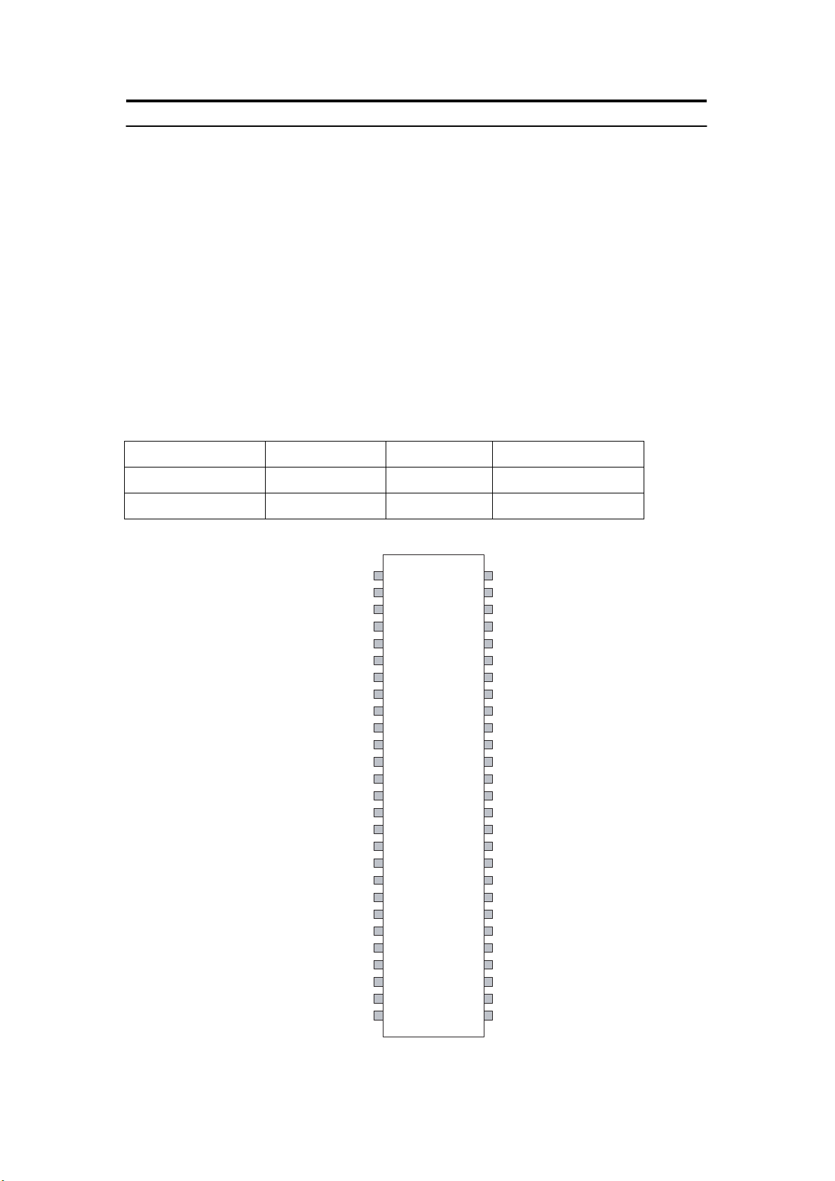
Pin Assignment
V
CC
DQ0
V
CCQ
NC
DQ1
V
SSQ
NC
DQ2
CCQ
V
NC
DQ3
SSQ
V
NC
CC
V
NC
/WE
/CAS
/RAS
/CS
BS0
BS1
A10/AP
A0
A1
A2
A3
CC
V
1
2
3
4
5
6
7
8
9
10
11
12
13
14
15
16
17
18
19
20
21
22
23
24
25
26
27 28
54
53
52
51
50
49
48
47
46
45
44
43
42
41
40
39
38
37
36
35
34
33
32
31
30
29
Vss
DQ7
Vss
NC
DQ6
V
CCQ
NC
DQ5
V
SSQ
NC
DQ4
V
CCQ
NC
V
SS
NC
DQM
CLK
CKE
A12
A11
A9
A8
A7
A6
A5
A4
V
SS
Q
54-pin plastic TSOP II 400 mil
Rev 1.0 December, 2001
1
A-Data ADS8608A8A
Pin Description
PIN NAME FUNCTION
CLK System Clock Active on the positive edge to sample all inputs.
CKE Clock Enable Masks system clock to freeze operation from the next clock cycle. CKE
should be enabled at least on cycle prior new command. Disable input
buffers for power down in standby
/CS Chip Select Disables or Enables device operation by masking or enabling all input
except CLK, CKE and L(U)DQM
A0~A12 Address Row / Column address are multiplexed on the same pins.
Row address : A0~A12
Column address : A0~A9
BS0~BS1 Banks Select Selects bank to be activated during row address latch time.
Selects bank for read / write during column address latch time.
DQ0~DQ7 Data Data inputs / outputs are multiplexed on the same pins.
/RAS Row Address Strobe Latches row addresses on the positive edge of the CLK with /RAS low
/CAS Column Address Strobe Latches Column addresses on the positive edge of the CLK with /CAS low
/WE Write Enable Enables write operation and row recharge.
VCC/VSS Power Supply/Ground Power and Ground for the input buffers and the core logic.
VCCQ/VSSQ Data Output Power/Ground Power supply for output buffers.
NC No Connection This pin is recommended to be left No Connection on the device.
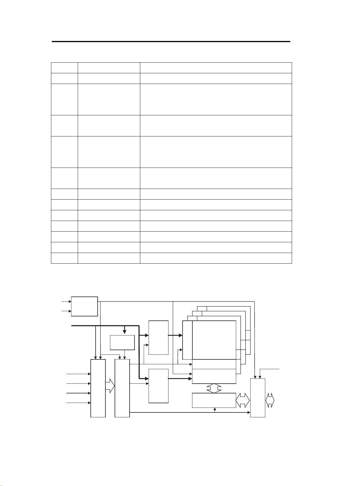
Block Diagram
CLK
CKE
Address
/CS
/RAS
/CAS
/WE
Clock
Generator
Mode
Register
Command Decoder
Control Logic
Address
Buffer
&
Refresh
Counter
Column
Address
Buffer
&
Refresh
Counter
Row Decoder
Amplifier
Column Decoder
Data Control Circuit
Bank3
Bank2
Bank1
Bank0
Data Latch
DQM
DQ
Rev 1.0 December, 2001
2
A-Data ADS8608A8A
Absolute Maximum Ratings
Parameter Symbol Value Unit
Voltage on any pin relative to Vss VIN, Vout -0.3 ~Vcc+0.3 V
Voltage on VDD supply relative to Vss VCC, VCCQ -0.3 ~ 4.6 V
Storage temperature TSTG -55 ~ +150
Power dissipation PD 1 W
Short circuit current IOUT 50 mA
Note : Permanent device damage may occur if ABSOLUTE MAXIMUM RATING are exceeded.
Functional operation should be restricted to recommended operating condition.
Exposure to higher than recommended voltage for extended periods of time could affect device reliability.
℃
DC Operating Condition
Voltage referenced to Vss = 0V, TA = 0 to 70 ℃
Parameter Symbol Min Typ Max Unit Note
Supply voltage VCC, VCCQ 3.0 3.3 3.6 V
Input logic high voltage VIH 2.0 3.0 VCC+0.3 V 2
Input logic low voltage VIL -0.3 - 0.8 V 2
Note : 1. VIH (max)=Vcc/ VccQ+1.2V for pulse width ≦ 5ns acceptable.
2.V
IL(min)=-Vss/ VssQ-1.2V for pulse width ≦ 5ns acceptable.
AC Operating Condition
Voltage referenced to Vss = 0V, TA = 0 to 70 ℃
Parameter Symbol Value Unit Note
AC input high / low level voltage VIH / VIL 2.4 / 0.4 V
Input timing measurement reference level voltage Vtrip 1.4 V
Input rise / fall time TR / tF 2 Ns
Output timing measurement reference level Voutfef 1.4 V
Output load capacitance for access time measurement CL 50 pF 2
Note: 1. 3.15V ≦ VDD ≦ 3.6V is applied for ADS8608A8A55.
2. Output load to measure access times is equivalent to two TTL gates and one capacitor (30pF). For details,
refer to AC/DC output load circuit.
Rev 1.0 December, 2001
3
 Loading...