

ACT ACT-S512K8N-055P4Q, ACT-S512K8N-055F4Q, ACT-S512K8N-055F3Q, ACT-S512K8N-045P4Q, ACT-S512K8N-045F4Q Datasheet
...
www.aeroflex.com
eroflex Circuit Technology - Advanced Multichip Modules © SCD1664 REV C 5/10/00
Features
ACT–S512K8 High Speed
4 Megabit Monolithic SRAM
■ Low Power Monolithic CMOS 512K x 8 SRAM
■ Full Military (-55°C to +125°C) Temperature Range
■ Input and Output TTL Compatible Design
■ Fast 17,20,25,35,45 & 55ns Maximum Access Times
■ +5 V Power Supply
■ MIL-PRF-38534 Compliant MCMs Available
■ Industry Standard Pinouts
■ Packaging – Hermetic Ceramic
● 36 Lead, .92" x .51" x .13" Flat Package (FP), Aeroflex code# "F3"
● 36 Lead, .92" x .43" x .184" Small Outline J lead (CSOJ),
Aeroflex code# "F4"
(.155 MAX thickness available, contact factory for details)
● 32 Lead, 1.6" x .60" x .20" Dual-in-line (DIP), Aeroflex code# "P4"
■ DESC SMD# 5962–95613 Released(F3,F4,P4)
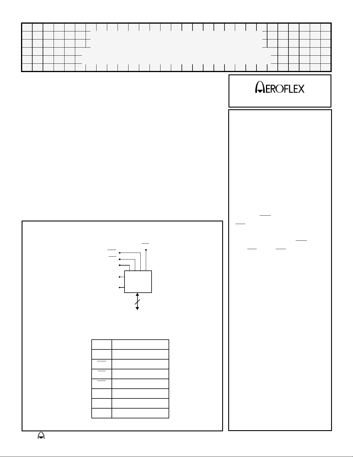
Block Diagram – Flat Package(F3,F16), DIP(P4) & CSOJ(F4)
CE
WE
OE
A0 – A18
Vss
Vcc
512Kx8
8
I/O0-7
CIRCUIT TECHNOLOGY
General Description
The ACT–S512K8 is a high
speed, 4 Megabit CMOS
Monolithic SRAM designed for
full temperature range military,
space, or high reliability mass
memory and fast cache
applications.
The MCM is input and output
TTL compatible. Writing is
executed when the write
enable (WE
(CE
) inputs are low and output
enable (OE) is high.Readingis
accomplished when WE
and CE
Access time grades of 17ns,
20ns, 25ns, 35ns, 45ns and
55ns maximum are standard.
The +5 Volt power supply
version is standard and +3.3
Volt lower power model is a
future optional product.
) and chip enable
is high
and OE are both low.
The products are designed
Pin Description
0-7 Data I/O
I/O
0–18 Address Inputs
A
for operation over the
temperature range of -55°C to
+125°C and under the full
military environment. A DESC
WE
CE
OE
CC Power Supply
V
SS Ground
V
NC Not Connected
Write Enable
Chip Enable
Output Enable
Standard Military Drawing
(SMD) number is released.
The ACT-S512K8 is
manufactured in Aeroflex’s
80,000 square foot
MIL-PRF-38534 certified
facility in Plainview, N.Y.
Absolute Maximum Ratings
Symbol Parameter MINIMUM MAXIMUM Units
-55 +125 °C
-65 +150 °C
- 1.1 W
-0.5 V
+ 0.5 V
CC
-0.5 +7.0 V
- +150 °C
T
V
T
STG
P
V
CC
T
C
Case Operating Temp.
Storage Temperature
D
G
Maximum Package Power Dissipation
Maximum Signal Voltage to Ground
Power Supply Voltage
J
Junction Temperature
Recommended Operating Conditions
Symbol Parameter Minimum Maximum Units
V
CC
V
IH
V
IL
T
A
Power Supply Voltage
Input High Voltage
Input Low Voltage
Operating Temp. (Mil)
+4.5 +5.5 V
+2.2 V
+ 0.3 V
CC
-0.5 +0.8 V
-55 +125 °C
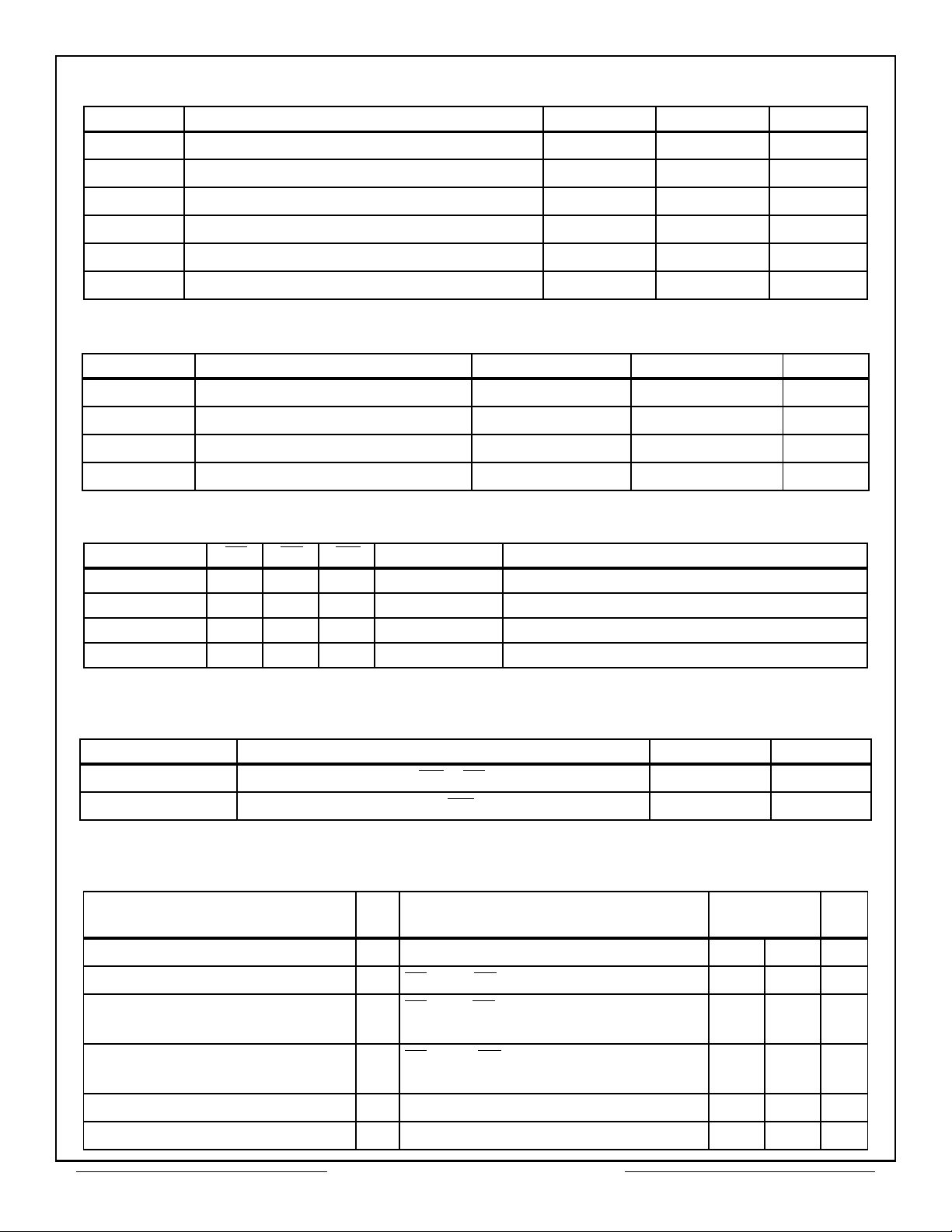
Truth Table
Mode CE OE WE Data I/O Power
Standby H X X High Z Standby (deselect/power down)
Read L L H Data OUT Active
Output Disable L H H High Z Active (deselected)
Write L X L Data IN Active
Capacitance
(V
= 0V, f = 1MHz, Tc = 25°C, unless otherwise noted, Guaranteed but not tested)
IN
Symbol Parameter Maximum Units
C
IN
C
OUT
Input Capacitance (A
0-18
Output Capacitance (I/O
, WE & OE)
& CE)
0-7
20 pF
20 pF
DC Characteristics
(VCC = 5.0V, VSS = 0V, Tc = -55°C to +125°C, unless otherwise specified)
Parameter Sym Conditions
I
Input Leakage Current
Output Leakage Current
Operating Supply Current
Standby Current
Output Low Voltage
Output High Voltage
VCC = Max, VIN=0toV
LI
I
CE = VIH, OE = VIH, V
LO
CE = VIL, OE = VIH, Vcc=5.5V,
I
CC
f=5MHz CMOS Compatible
CE = Vcc, OE= VIH, Vcc=5.5V,
I
SB
f=5MHz CMOS Compatible
V
IOL = 8 mA, Vcc = 4.5V
OL
V
IOH = -4 mA, Vcc = 4.5V
OH
CC
OUT
= 0toV
CC
ALL SPEEDS
Min Max
-10 +10 µA
-10 +10 µA
- 170 mA
- 20 mA
- 0.4 V
2.4 - V
Units
Aeroflex Circuit Technology SCD1664 REV C 5/10/00 Plainview NY (516) 694-6700
2
Read Cycle
Parameter
Read Cycle Time
Address Access Time
Chip Select Access Time
Output Hold from Address Change
Output Enable to Output Valid
Chip Select to Output in Low Z (1)
Output Enable to Output in Low Z (1)
Chip Deselect to Output in High Z (1)
Output Disable to Output in High Z (1)
Note 1. Guaranteed by design, but not tested
Write Cycle
Parameter
Write Cycle Time
Chip Select to End of Write
Address Valid to End of Write
Data Valid to End of Write
Write Pulse Width
Address Setup Time
Address Hold Time
Output Active from End of Write (1)
Write to Output in High Z (1)
Data Hold from Write Time
Note 1. Guaranteed by design, but not tested
AC Characteristics
(VCC = 5.0V, VSS= 0V, Tc= -55°C to +125°C)
Sym
t
t
t
t
t
Sym
t
t
t
t
t
–017
Min Max
17 - 20 - 25 - 35 - 45 - 55 -
t
RC
- 17 - 20 - 25 - 35 - 45 - 55
t
AA
- 17 - 20 - 25 - 35 - 45 - 55
ACS
0 - 0 - 0 - 0 - 0 - 0 -
t
OH
- 9 - 10 - 12 - 25 25 25 ns
t
OE
2 - 2 - 2 - 4 - 4 - 4 - ns
CLZ
0 - 0 - 0 - 0 - 0 - 0 -
OLZ
- 9 - 10 - 12 - 15 - 20 - 20
CHZ
- 9 - 10 - 12 - 15 - 20 - 20
OHZ
–017
Min Max
17 - 20 - 25 - 35 - 45 - 55 - ns
WC
15 - 15 - 20 - 25 - 35 - 50 - ns
CW
t
15 - 15 - 20 - 25 - 35 - 50 - ns
AW
12 - 12 - 15 - 20 - 25 - 25 - ns
DW
t
14 - 14 - 15 - 25 - 35 - 40 - ns
WP
t
2 - 2 - 2 - 2 - 2 - 2 - ns
AS
t
0 - 0 - 0 - 0 - 5 - 5 - ns
AH
0 - 0 - 0 0 5 - 5 - ns
OW
- 9 - 9 - 10 - 15 - 20 - 25 ns
WHZ
t
0 - 0 - 0 - 0 - 0 - 0 - ns
DH
–020
Min Max
–020
Min Max
–025
Min Max
–025
Min Max
Min Max
Min Max
–035
–035
–045
Min Max
–045
Min Max
–055
Min Max
–055
Min Max
Units
ns
ns
ns
ns
ns
ns
ns
Units
Data Retention Electrical Characteristics (Special Order Only)
(Tc = -55°C to +125°C)
Parameter Sym Test Conditions
for Data Retention
V
CC
Data Retention Current (1)
Available in Low Power version. Call For Information.
V
DR
I
CCDR1
CE ≥ V
V
CC
CC
= 3V
– 0.2V
ALL SPEEDS
Min Typ Max
2 - 5.5 V
- 0.5 7.0 mA
Units
Truth Table
Mode CE OE WE Data I/O Power
Standby H X X High Z Standby (deselect/power down)
Read L L H Data Out Active
Output Disable L H H High Z Active (deselected)
Write L X L Data In Active
Aeroflex Circuit Technology SCD1664 REV C 5/10/00 Plainview NY (516) 694-6700
3
 Loading...