

ACT ACT-PS512K8Y-020L2T, ACT-PS512K8Y, ACT-PS512K8X, ACT-PS512K8W, ACT-PS512K8N Datasheet
...
CIRCUIT TECHNOLOGY
www.aeroflex.com
eroflex Circuit Technology - Advanced Multichip Modules © SCD3764 REV A 6/2/98
General Description
The ACT-PS512K8 is a
Plastic High Speed, 4 Megabit
(4,194,304 bits) CMOS
Monolithic SRAM organized as
524,288 words by 8 bits.
Designed for high-speed, high
density, high reliablility, mass
memory and fast cache system
applications.
The plastic monolithic is
input and output TTL
compatible.Writingisexecuted
when the write enable (WE
)
and chip enable (CE
) inputs are
low. Reading is accomplished
when WE
is high and CE and
output enable (OE
) are both
low. Access time grades of
10ns 12ns, 15ns, 17ns, 20ns
and 25ns are standard.
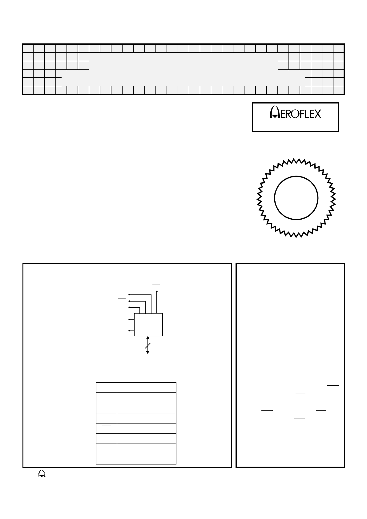
512Kx8
OE
A0 – A18
I/O0-7
8
WE
CE
Pin Description
I/O
0-7 Data I/O
A
0–18 Address Inputs
WE
Write Enable
CE
Chip Enable
OE
Output Enable
V
CC Power Supply
V
SS Ground
NC Not Connected
Vss
Vcc
Block Diagram – SOJ (L2)
Plastic Path™ Features
■ Low Power Monolithic CMOS 512K x 8 SRAM
■ Operating Temperature Range
● Full Military (-55°C to +125°C)
● Industrial (-40°C to +85°C)
■ Burn-in and Temperature Cycle Available
■ 10, 12, 15, 17, 20 & 25ns Access Times
■ +5V Power Supply
■ Industry Standard Pinouts
● Center Power / Ground Pins
■ TTL Compatible I/O
■ 3.3V Device I/O Interfacing
■ JEDEC Standard 36 pin Plastic SOJ Package
● 36 Lead, .93" x .405" x 0.148 Small Outline J lead (SOJ),
Aeroflex code# "L2"
■ Fully Static Operation
● No Clocks or Refresh Required
4 Megabit Plastic Monolithic SRAM
ACT-PS512K8 High Speed
F
I
E
I
D
C
E
R
T
A
E
R
O
F
L
E
X
L
A
B
S
I
N
C
.
ISO
900
1
Aeroflex Circuit Technology SCD3764 REV A 6/2/98 Plainview NY (516) 694-6700
2
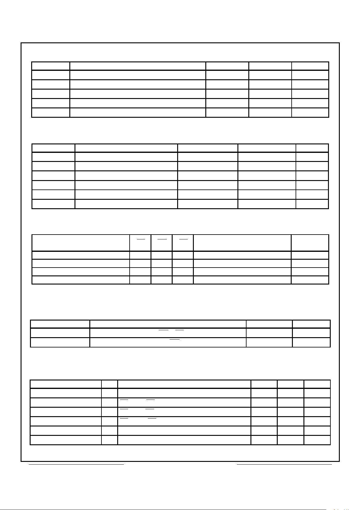
Absolute Maximum Ratings
Symbol Parameter MINIMUM MAXIMUM Units
T
C
Case Operating Temperature
-55 +125 °C
T
STG
Storage Temperature
-65 +150 °C
P
D
Maximum Package Power Dissipation
1.0 W
V
G
Maximum Signal Voltage to Ground
-0.5 V
CC
+ 0.5 V
V
CC
Power Supply Voltage
-0.5 +7.0 V
Recommended Operating Conditions
Symbol Parameter Minimum Maximum Units
V
CC
Power Supply Voltage
+4.5 +5.5 V
V
SS
Ground
0 0 V
V
IH
Input High Voltage
+2.2 V
CC
+ 0.5 V
V
IL
Input Low Voltage
-0.5 +0.8 V
T
C
Operating Temperature (Military)
-55 +125 °C
T
C
Operating Temperature (Industrial)
-40 +85 °C
Truth Table
Mode CE WE OE Data I/O
Supply
Current
Standby H X X High Z I
SB
Output Disable L H H High Z I
CC
Read L H L Data OUT I
CC
Write L L X Data IN I
CC
Capacitance
(VIN & V
OUT
= 0V, f = 1MHz, TC = 25°C, unless otherwise noted, Guaranteed but not tested)
Symbol Parameter Maximum Units
C
IN
Input Capacitance (A
0-18
, WE & OE)
6 pF
C
OUT
Output Capacitance (I/O
0-7
& CE)
8 pF
DC Characteristics
(VCC = 5.0V, VSS = 0V, TC = -55°C to +125°C or -40°C to +85°C)
Parameter Sym Conditions Min Max Units
Input Leakage Current
I
LI
VCC = Max, VIN=VSStoV
CC
-10 +10 µA
Output Leakage Current
I
LO
CE = VIH, OE = VIH, V
OUT
= VSStoV
CC
-10 +10 µA
Operating Supply Current
I
CC
CE = VIL, OE = VIH,f=5MHz,Vcc=5.5V
130 mA
Standby Current
I
SB
CE = VIH, OE= VIH, f=5MHz,Vcc=5.5V
20 mA
Output Low Voltage
V
OL
IOL = 8 mA, Vcc = 4.5V
0.4 V
Output High Voltage
V
OH
IOH = -4 mA, Vcc = 4.5V
2.4 V
Note: DC Test conditions: VIL = 0.3V, VIH = Vcc - 0.3V.
 Loading...