

ACT ACT-PD1M16W-070L4I, ACT-PD1M16N-070L4T, ACT-PD1M16N, ACT-PD1M16Y-070L4T, ACT-PD1M16Y Datasheet
...
www.aeroflex.com
eroflex Circuit Technology - Advanced Multichip Modules © SCD3750 REV A 8/31/98
ACT–PD1M16 Fast Page Mode
F
E
I
D
C
E
R
T
A
E
R
O
F
L
E
X
L
A
B
S
I
N
C
.
16 Megabit Plastic Monolithic DRAM
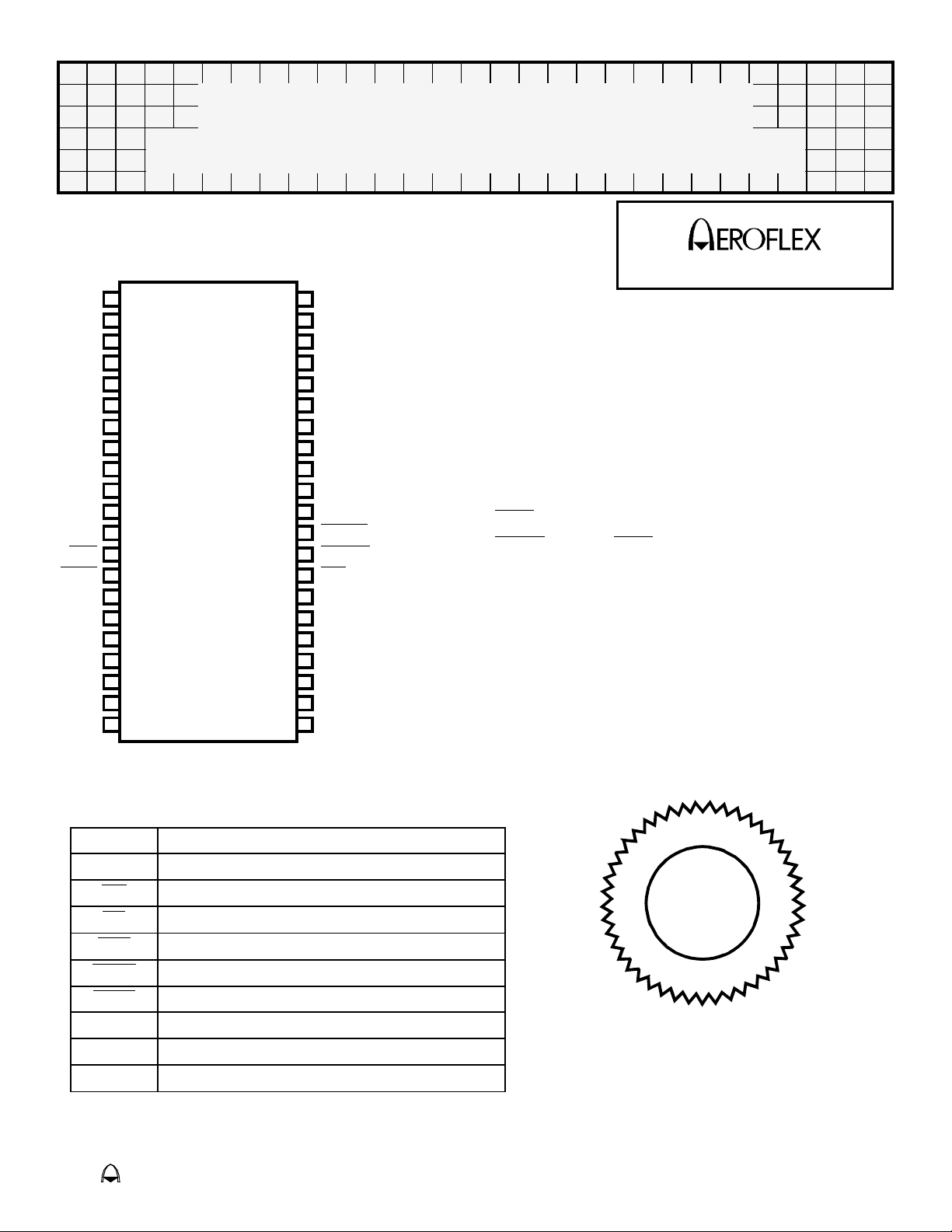
Vcc
I/O0
I/O1
I/O2
I/O3
Vcc
I/O4
I/O5
I/O6
I/O7
NC
NC
WE
RAS
NC
NC
A0
A1
A2
A3
Vcc
Pin Configuration
Top View
1
2
3
4
5
6
7
8
9
10
11
12
13
14
15
16
17
18
19
20
21
42
41
40
39
38
37
36
35
34
33
32
31
30
29
28
27
26
25
24
23
22
VSS
I/O15
I/O14
I/O13
I/O12
SS
V
I/O11
I/O10
I/O9
I/O8
NC
LCAS
UCAS
OE
A9
A8
A7
A6
A5
A4
SS
V
CIRCUIT TECHNOLOGY
Features
■ Fast Access Time (tRAC): 70ns
■ Power Supply: 5.0V ± 0.5V
■ Packaging
● 42 Lead Plastic Surface-Mount SOJ (L4)
■ Industrial and Military Temperature Ranges
■ Three-State Unlatched Output
■ Fast Page Mode
■ RAS-Only Refresh
■ xCAS Before RAS Refresh
■ Hidden Refresh
■ 1024 Cycle Refresh in 16ms
■ Low Power Dissipation
■ Long Refresh Period Option
Pin Description
0–9 Address Inputs
A
0-15 Data Input / Output
I/O
WE
Read/Write Enable
OE
RAS
UCAS
LCAS
CC +5.0V Power Supply
V
SS Ground
V
NC Not Connected
Upper Byte Control / Column Address Strobe
Lower Byte Control / Column Address Strobe
Output Enable
Row Address Strobe
ISO
900
1
I
Absolute Maximum Ratings
Symbol Parameter MINIMUM MAXIMUM Units
T
C
T
STG
I
OS
P
T
V
CC
V
T
Stresses beyond those listed under “absolute maximum ratings” may cause permanent damage to the device. These are
stress ratings only, and functional operation of the device at these or any other conditions beyond those indicated under
“recommended operating conditions” is not implied. Exposure to absolute-maximum rated conditions for extended periods may
affect device reliability.
* All voltage values are with respect to Vss.
Case Operating Temp.
Storage Temperature
Short Circuit Output Current
Power Dissipated
Supply Voltage Range
Voltage Range on any Pin*
-55 +125 °C
-55 +150 °C
- 50 mA
- 1 W
-1.0 +7.0 V
-1.0 +7.0 V
Recommended Operating Conditions
Symbol Parameter Minimum Maximum Units
V
CC
V
IH
V
IL
T
CM
T
CI
Power Supply Voltage
Input High Voltage
Input Low Voltage
Operating Temp. (Mil)
Operating Temp. (Ind.)
+4.5 +5.5 V
+2.4 - V
- +0.8 V
-55 +125 °C
-40 +85 °C
Capacitance
(V
= 0V, f = 1MHz, Tc = 25°C)
IN
Symbol Parameter Maximum Units
C
I(A)
C
I(RC)
C
I(OE)
C
I(WE)
C
O
These parameters are guaranteed by design but not tested.
A
Input Capacitance
0-9
RAS and CAS Input Capacitance
OE Input Capacitance
WE Input Capacitance
Output Capacitance
10 pF
10 pF
10 pF
10 pF
15 pF
DC Characteristics
(VCC = 5.0V, VSS = 0V, TCI or TCM)
Parameter Sym Conditions Min Max Units
Output Low Voltage
Output High Voltage
Input Leakage Current
Output Leakage Current
Read or Write Cycle Current
1,2
V
IOL = 4.2 mA
OL
V
IOH = -5 mA
OH
I
VI=0to+6.5V, All others 0V to V
L
I
I
CC1
O
VO=0toV
V
= 5.5V, minimum cycle
CC
CAS high
CC,
CC
- 0.4 V
2.4 V
-10 +10 µA
-10 +10 µA
190 mA
Aeroflex Circuit Technology SCD3750 REV A 8/31/98 Plainview NY (516) 694-6700
2
DC Characteristics (continued)
(VCC = 5.0V, VSS = 0V, T CI or TCM)
Parameter Sym Conditions Min Max Units
VIH = 2.4V (TTL), After 1 memory cycle,
I
CC2
Standby Current
I
CC3
Average Page Current
1. Measured with a maximum of one address change while RAS = VIL.
2. Measured with a maximum of one address change while CAS
2
I
CC4
and CAS high
RAS
VIH = Vcc - 0.05V (CMOS), After 1 memory
cycle, RAS
and CAS high
RAS low, CAS cycling
= VIH.
- 2 mA
- 1 mA
- 100 mA
AC Characteristics*
(VCC = 5.0V ±10%, VSS= 0V, TCI or TCM)
Parameter
Access Time from Column-Address
Low Access Time from CAS
CAS
Column Access Time from CAS
Precharge
Access Time from RAS
Access Time
OE
1
Output Buffer Turn-off Delay
Output Buffer Turn-off Delay Time from OE
* Valid data is presented at the outputs after all access times are satisfied but can go from the high-impedance
state to an invalid-data state prior to the specified access times as the outputs are driven when CAS
OFF and tOEZ are specified when the outputs are no longer driven. The outputs are disabled by bringing either
1. t
or CAS high.
OE
1
Sym Min Max Units
AA - 35 ns
t
tCAC - 20 ns
tCPA - 40 ns
tRAC - 70 ns
tOEA - 20 ns
tOFF 0 15 ns
tOEZ 0 15 ns
goes low.
AC Characteristics
(VCC = 5.0V, VSS = 0V, TCI or TCM)
Parameter
Cycle Time, Read or Write Random 1
Cycle Time, Fast Page Mode Read or Write
Cycle Time, Fast Page Mode Read-Modify-Write
Pulse Duration, RAS Low Fast Page Mode
Pulse Duration, RAS Low Nonpage Mode
Pulse Duration, CAS Low
4
Pulse Duration, CAS High Precharge Time
Pulse Duration, RAS High Precharge Time
Pulse Duration, WE Low
Setup Time, Column Address before CAS Low
Setup Time, Row Address before RAS Low
Setup Time, Data
5
Setup Time, WE High before CAS Low
Setup Time, WE Low before CAS High
Setup Time, WE Low before RAS High
1,2
3
3
Sym Min Max Units
RC 130 -
t
tPC 45 -
1
tPRWC 90 -
tRASP 70 200,000
tRAS 70 10,000 ns
tCAS 20 10,000 ns
tCP 10 -
tRP 50 -
tWP 15 -
tASC 0 -
tASR 0 - ns
ns
ns
ns
ns
ns
ns
ns
ns
tDS 0 - ns
t
t
t
RCS
CWL
RWL
0 - ns
20 - ns
20 - ns
Aeroflex Circuit Technology SCD3750 REV A 8/31/98 Plainview NY (516) 694-6700
3
 Loading...