

ACT ACT-F512K8N-150P4Q, ACT-F512K8N-150F7Q, ACT-F512K8N-150F6Q, ACT-F512K8N-120P4Q, ACT-F512K8N-120F7Q Datasheet
...
www.aeroflex.com
Features
ACT–F512K8 High Speed
4 Megabit Monolithic FLASH
CIRCUIT TECHNOLOGY
■ Low Power Monolithic 512K x 8 FLASH
■ TTL Compatible Inputs and CMOS Outputs
■ Access Times of 60, 70, 90, 120 and 150ns
■ +5V Programing, 5V ±10% Supply
■ 100,000 Erase / Program Cycles
■ Low Standby Current
■ Page Program Operation and Internal
Program Control Time
■ Supports Full Chip Erase
■ Embedded Erase and Program Algorithms
■ Supports Full Chip Erase
■ MIL-PRF-38534 Compliant Circuits Available
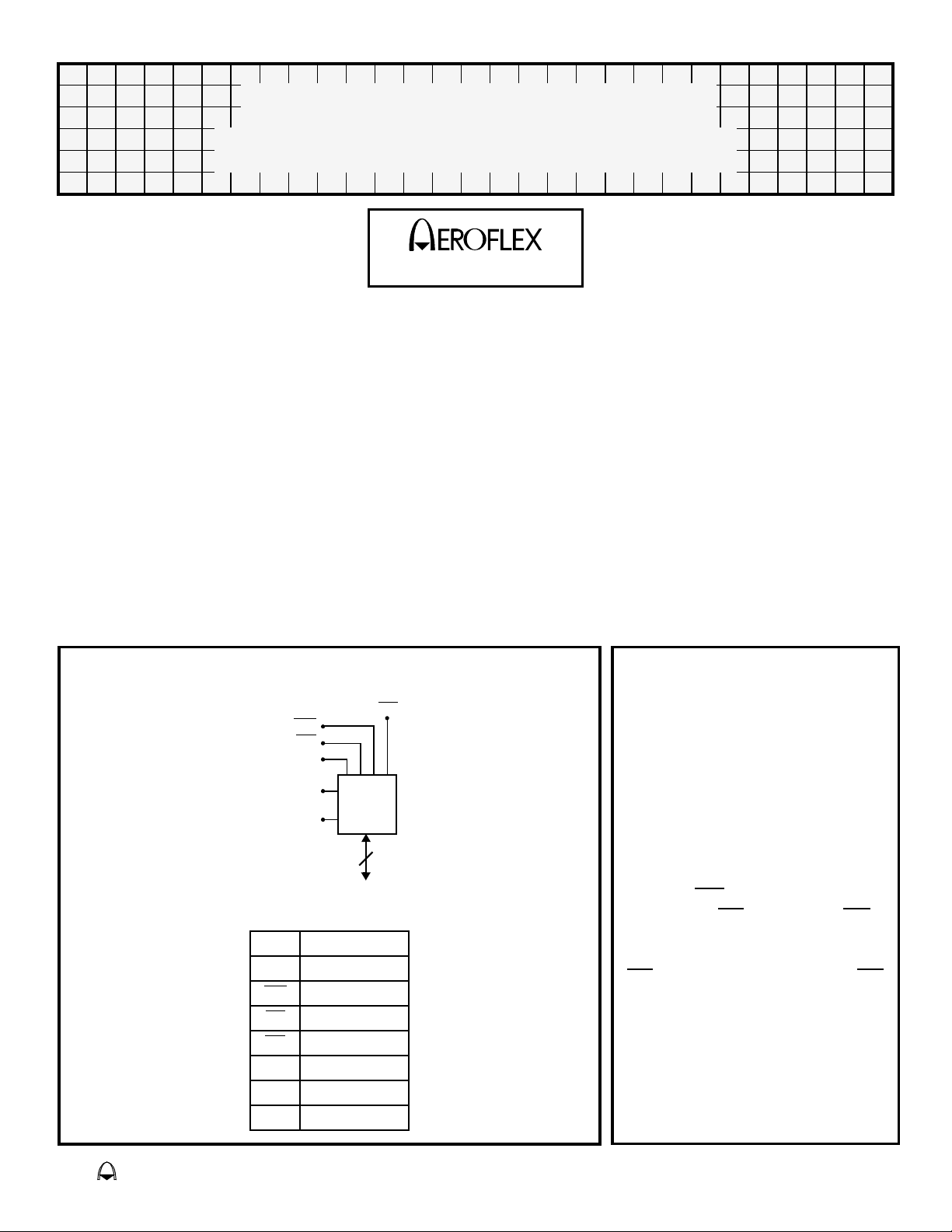
Block Diagram – DIP (P4) & Flat Packages (F6,F7)
CE
WE
OE
A0 – A18
Vss
Vcc
Pin Description
I/O
0-7 Data I/O
A
0–18 Address Inputs
WE
CE
OE
V
CC Power Supply
V
SS Ground
NC Not Connected
512Kx8
8
I/O0-7
Write Enable
Chip Enable
Output Enable
■ Industry Standard Pinouts
■ Packaging – Hermetic Ceramic
● 32 Lead, 1.6" x .6" x .20" Dual-in-line Package (DIP),
Aeroflex code# "P4"
● 32 Lead, .82" x .41" x .11" Ceramic Flat Package
(FP), Aeroflex code# "F6"
● 32 Lead, .82" x .41" x .132" Ceramic Flat Package
(FP Lead Formed), Aeroflex code# "F7"
■ Sector Architecture
● 8 Equal size sectors of 64K bytes each
● Any Combination of Sectors ccan be erased with one
command sequence.
■ Commercial, Industrial and Military
Temperature Ranges
■ DESC SMD Pending
5962-96692 (P4,F6,F7)
General Description
The ACT–F512K8 is a high
speed, 4 megabit CMOS
monolithic Flash module
designed for full temperature
range military, space, or high
reliability applications.
This device is input TTL and
output CMOS compatible. The
command register is written by
bringing WE
IL), while CE is low and OE is
(V
at logic high level (V
is accomplished by chip Enable
) and Output Enable (OE)
(CE
being logically active, see
Figure9. Access time grades of
60ns, 70ns, 90ns, 120ns and
150ns maximum are standard.
The ACT–F512K8 is
available in a choice of
to a logic low level
IH). Reading
eroflex Circuit Technology - Advanced Multichip Modules © SCD1668 REV A 4/28/98

General Description, Cont’d,
hermetically sealed ceramic packages; a
32 lead .82" x .41" x .11"flat package in
both formed or unformed leads or a 32 pin
1.6"x.60" x.20" DIP package for operation
over the temperature range -55°C to
+125°C and military environmental
conditions.
The flash memory is organized as
512Kx8 bits and is designed to be
programmed in-system with the standard
system 5.0V Vcc supply. A 12.0V V
PP is
not required for write or erase operations.
The device can also be reprogrammed with
standard EPROM programmers (with the
proper socket).
The standard ACT–F512K8 offers
access times between 60ns and 150ns,
allowing operation of high-speed
microprocessors without wait states. To
eliminate bus contention, the device has
separate chip enable (CE
) and output enable (OE) controls. The
(WE
), write enable
ACT–F512K8 is command set compatible
with JEDEC standard 1 Mbit EEPROMs.
Commands are written to the command
register using standard microprocessor
write timings. Register contents serve as
input to an internal state-machine which
controls the erase and programming
circuitry. Write cycles also internally latch
addresses and data needed for the
programming and erase operations.
Reading data out of the device is similar
to reading from 12.0V Flash or EPROM
devices. The ACT–F512K8 is programmed
by executing the program command
sequence. This will invoke the Embedded
Program Algorithm which is an internal
algorithm that automatically times the
program pulse widths and verifies proper
cell margin. Typically, each sector can be
programmed and verified in less than 0.3
second. Erase is accomplished by
executing the erase command sequence.
This will invoke the Embedded Erase
Algorithm which is an internal algorithm
that automatically preprograms the array, (if
it is not already programmed before)
executing the erase operation. During
erase, the device automatically times the
erase pulse widths and verifies proper cell
margin.
The device is typically erased and
verified in 1.5 seconds (if already
completely preprogrammed).
Also the device features a sector erase
architecture. The sector mode allows for
64K byte blocks of memory to be erased
and reprogrammed without affecting other
blocks. The ACT-F512K8 is erased when
shipped from the factory.
The device features single 5.0V power
supply operation for both read and write
functions. lnternally generated and
regulated voltages are provided for the
program and erase operations. A low V
CC
detector automatically inhibits write
operations on the loss of power. The end of
program or erase is detected by Data
Polling of D7 or by the Toggle Bit feature on
D6. Once the end of a program or erase
cycle has been completed, the device
internally resets to the read mode.
All bits of each die, or all bits within a
sector of a die, are erased via
Fowler-Nordhiem tunneling. Bytes are
programmed one byte at a time by hot
electron injection.
A DESC Standard Military Drawing
(SMD) number is pending.
Aeroflex Circuit Technology SCD1668 REV A 4/28/98 Plainview NY (516) 694-6700
2
z
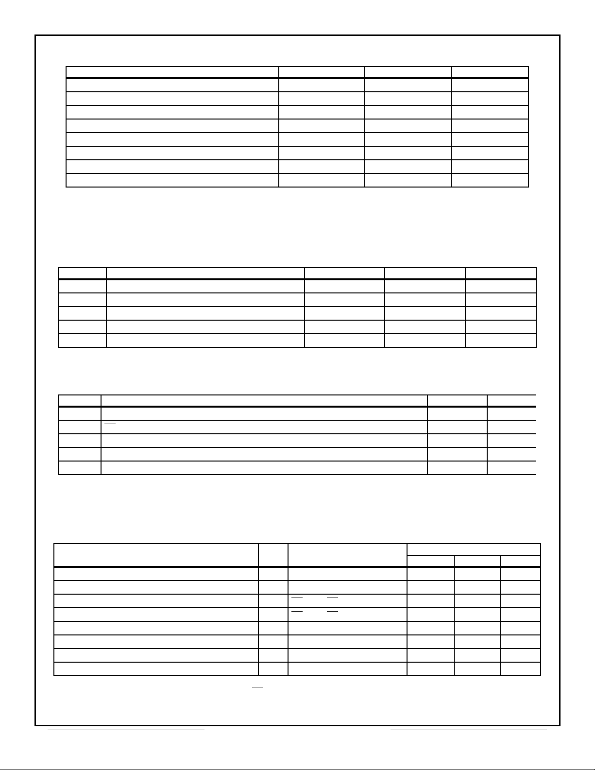
Absolute Maximum Ratings
Parameter Symbol Range Units
C -55 to +125 °C
Case Operating Temperature
Storage Temperature Range
Supply Voltage Range
Signal Voltage Range (Any Pin Except A9) Note 1
Maximum Lead Temperature (10 seconds)
Data Retention
Endurance (Write/Erase cycles)
A9 Voltage for sector protect, Note 2
Note 1. Minimum DC voltage on input or I/O pins is -0.5V. During voltage transitions, inputs may undershoot V
up to 20ns. Maximum DC voltage on input and I/O pins is V
overshoot to V
Note 2. Minimum DC input voltage on A9 is -0.5V. During voltage transitions, A9 may undershoot VSS to -2.0V for periods of up to 20ns.
CC + 2.0V for periods up to 20 ns.
T
STG -65 to +150 °C
T
CC -2.0 to +7.0 V
V
G -2.0 to +7.0 V
V
300 °C
10 Years
100,000 Minimum
ID -2.0 to +14.0 V
V
CC + 0.5V. During voltage transitions, inputs and I/O pins may
SS to -2.0v for periods of
Maximum DC input voltage on A9 is +12.5V which may overshoot to 14.0V for periods up to 20ns.
Normal Operating Conditions
Symbol Parameter Minimum Maximum Units
CC
V
V
V
Tc
V
Power Supply Voltage
IH
Input High Voltage
IL
Input Low Voltage
Operating Temperature (Military)
ID
A9 Voltage for sector protect
+4.5 +5.5 V
+2.0 V
+ 0.5 V
CC
-0.5 +0.8 V
-55 +125 °C
11.5 12.5 V
Capacitance
(VIN= 0V, f = 1MHz, Tc = 25°C)
Symbol Parameter Maximum Units
AD
C
C
C
C
C
A0 – A18 Capacitance
OE
OE Capacitance
WE
Write Enable Capacitance
CE
Chip Enable Capacitance
I/O
I/O0 – I/O7 Capacitance
15 pF
15 pF
15 pF
15 pF
15 pF
Parameters Guaranteed but not tested
DC Characteristics – CMOS Compatible
(Vcc = 5.0V, Vss = 0V, Tc = -55°C to +125°C, unless otherwise indicated)
Parameter Sym Conditions
LI
I
CC = 5.5V, VIN = GND to VCC
Input Leakage Current
Output Leakage Current
Active Operating Supply Current for Read (1)
Active Operating Supply Current for Program or Erase (2)
Operating Standby Supply Current
Output Low Voltage
Output High Voltage
Low Power Supply Lock-Out Voltage (4)
V
LOX32
I
I
I
I
V
V
CC = 5.5V, VIN = GND to VCC
V
CC1
CC2
CC3
OL
V
OH
LKO 3.2 V
= VIL, OE = VIH, f = 5MHz
CE
= VIL, OE = VIH
CE
CC = 5.5V, CE = VIH, f = 5MHz
V
IOL = +8.0 mA, VCC = 4.5V
IOH = –2.5 mA, VCC = 4.5V
Note 1. The Icc current listed includes both the DC operating current and the frequency dependent component (At 6 MHz). The frequency
component typically is less than 2 mA/MHz, with OE
Note 2. Icc active while Embedded Algorithm (Program or Erase) is in progress.
Note 3. DC Test conditions: V
IL = 0.3V, VIH = VCC - 0.3V, unless otherwise indicated.
at VIN.
Note 4. Parameter Guaranteed by design, but not tested.
Speeds 60, 70, 90, 120 & 150ns
Minimum Maximum Units
10 µA
10 µA
50 mA
60 mA
1.6 mA
0.45 V
0.85 x V
CC V
Aeroflex Circuit Technology SCD1668 REV A 4/28/98 Plainview NY (516) 694-6700
3
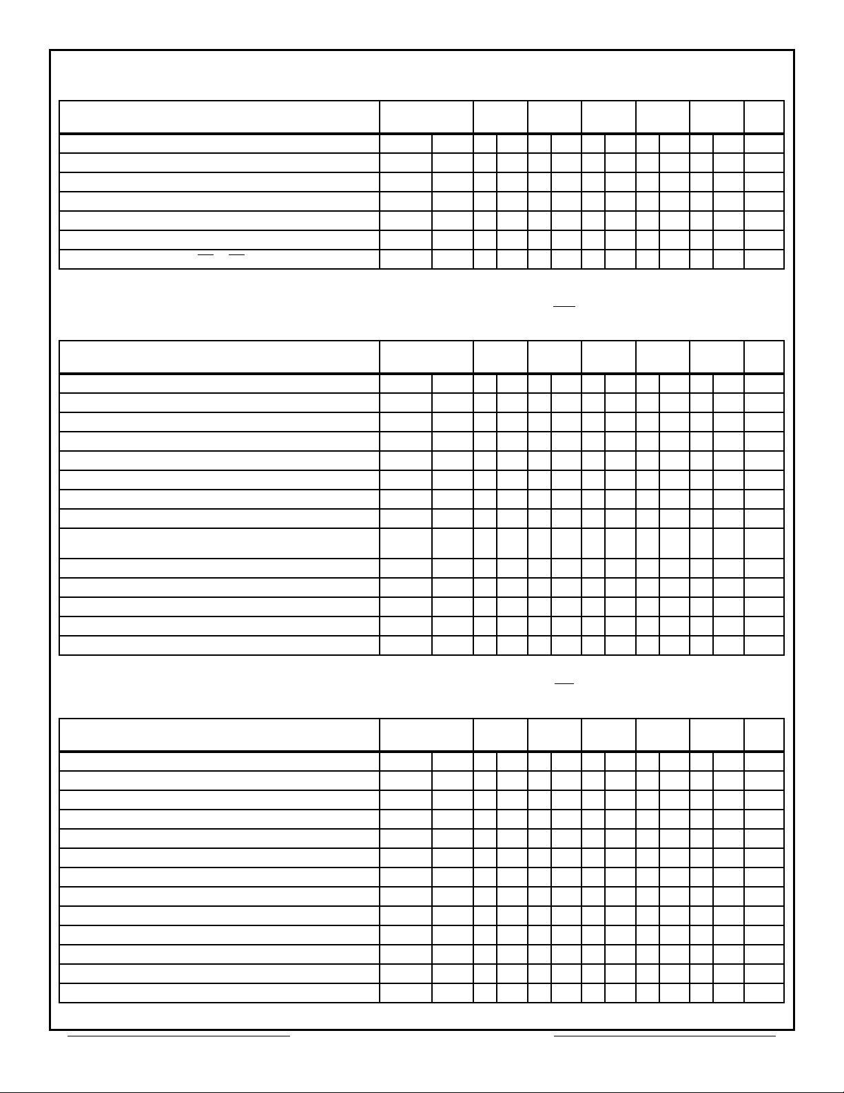
Parameter
Read Cycle Time
Address Access Time
Chip Enable Access Time
Output Enable to Output Valid
Chip Enable to Output High Z (1)
Output Enable High to Output High Z(1)
Output Hold from Address, CE
or OE Change, Whichever is First
Note 1. Guaranteed by design, but not tested
AC Characteristics – Write/Erase/Program Operations, WE Controlled
Parameter
Write Cycle Time
Chip Enable Setup Time
Write Enable Pulse Width
Address Setup Time
Data Setup Time
Data Hold Time
Address Hold Time
Write Enable Pulse Width High
Duration of Byte Programming Operation
Typ = 16 µs
Sector Erase Time
Read Recovery Time before Write
Vcc Setup Time
Chip Programming Time
Chip Erase Time
AC Characteristics – Read Only Operations
(Vcc = 5.0V, Vss = 0V, Tc = -55°C to +125°C)
Symbol
JEDEC Stand’d
AVAV tRC 60 70 90 120 150 ns
t
AVQV tACC 60 70 90 120 150 ns
t
ELQV tCE 60 70 90 120 150 ns
t
GLQV tOE 30 35 35 50 55 ns
t
EHQZ tDF 20 20 20 30 35 ns
t
GHQZ tDF 20 20 20 30 35 ns
t
t
AXQX tOH 0 0 0 0 0 ns
(Vcc = 5.0V, Vss = 0V, Tc = -55°C to +125°C)
Symbol
JEDEC Stand’d
AVAC tWC 60 70 90 120 150 ns
t
ELWL tCE 0 0 0 0 0 ns
t
WLWH tWP 40 45 45 50 50 ns
t
AVWL tAS 0 0 0 0 0 ns
t
DVWH tDS 40 45 45 50 50 ns
t
WHDX tDH 0 0 0 0 0 ns
t
WLAX tAH 45 45 45 50 50 ns
t
WHWL tWPH 20 20 20 20 20 ns
t
WHWH1 14 TYP 14 TYP 14 TYP 14 TYP 14 TYP µs
t
WHWH2 30 30 30 30 30 Sec
t
GHWL 0 0 0 0 0 µs
t
VCE 50 50 50 50 50 µs
t
WHWH3 120 120 120 120 120 Sec
t
–60
Min Max
–60
Min Max
–70
Min Max
–70
Min Max
50 50 50 50 50 Sec
–90
Min Max
–90
Min Max
–120
Min Max
–120
Min Max
–150
Min Max
–150
Min Max
Units
Units
AC Characteristics – Write/Erase/Program Operations, CE Controlled
(Vcc = 5.0V, Vss = 0V, Tc = -55°C to +125°C)
Parameter
Write Cycle Time
Write Enable Setup Time
Chip Enable Pulse Width
Address Setup Time
Data Setup Time
Data Hold Time
Address Hold Time
Chip Select Pulse Width High
Duration of Byte Programming
Sector Erase Time
Read Recovery Time
Symbol
JEDEC Stand’d
AVAC tWC 60 70 90 120 150 ns
t
WLEL tWS 0 0 0 0 0 ns
t
ELEH tCP 40 45 45 50 55 ns
t
AVEL tAS 0 0 0 0 0 ns
t
DVEH tDS 40 45 45 50 55 ns
t
EHDX tDH 0 0 0 0 0 ns
t
ELAX tAH 45 45 45 50 55 ns
t
EHEL tCPH 20 20 20 20 20 ns
t
WHWH1 14 TYP 14 TYP 14 TYP 14 TYP 14 TYP µs
t
WHWH2 30 30 30 30 30 Sec
t
tGHEL 0 0 0 0 0 ns
Chip Programming Time
WHWH3 120 120 120 120 120 Sec
Chip Erase Time
Aeroflex Circuit Technology SCD1668 REV A 4/28/98 Plainview NY (516) 694-6700
t
4
–60
Min Max
–70
Min Max
–90
Min Max
–120
Min Max
–150
Min Max
50 50 50 50 50 Sec
Units
Device Operation
The ACT–F512K8 Monolithic is composed of One, Four
megabit flash device. Programming of the ACT–F512K8
is accomplished by executing the program command
sequence. The program algorithm, which is an internal
algorithm, automatically times the program pulse widths
and verifies proper cell status. Sectors can be programed and verified in less than 1 second. Erase is
accomplished by executing the erase command
sequence. The erase algorithm, which is internal, automatically preprograms the array if it is not already programed before executing the erase operation. During
erase, the device automatically times the erase pulse
widths and verifies proper cell status. The entire memory is typically erased and verified in 1.5 seconds (if
pre-programmed). The sector mode allows for 64K byte
blocks of memory to be erased and reprogrammed without affecting other blocks.
Bus Operation
READ
The ACT–F512K8 has two control functions, both of
which must be logically active, to obtain data at the outputs. Chip Enable (CE
be used for device selection. Output-Enable (OE
output control and should be used to gate data to the
output pins of the chip selected. Figure 7 illustrates AC
read timing waveforms.
OUTPUT DISABLE
With Output-Enable at a logic high level (VIH), output
from the device is disabled. Output pins are placed in a
high impedance state.
STANDBY MODE
The ACT-F512K8 standby mode consumes less than 6.5
mA. In the standby mode the outputs are in a high
impedance state, independent of the OE
device is deselected during erasure or programming, the
device will draw active current until the operation is completed.
) is the power control and should
) is the
input. If the
WRITE
Device erasure and programming are accomplished via
the command register. The contents of the register
serve as input to the internal state machine. The state
machine outputs dictate the function of the device.
The command register itself does not occupy an addressable memory location. The register is a latch used to
store the command, along with address and data information needed to execute the command. The command
register is written by bringing WE
IL), while CE is low and OE is at VIH. Addresses are
(V
latched on the falling edge of WE
to a logic low level
or CE, whichever happens later. Data is latched on the rising edge of the WE
or CE whichever occurs first. Standard microprocessor
write timings are used. Refer to AC Program Characteristics and Waveforms, Figures 3, 8and13.
Command Definitions
Device operations are selected by writing specific
address and data sequences into the command register.
Table 3 defines these register command sequences.
READ/RESET COMMAND
The read or reset operation is initiated by writing the
read/reset command sequence into the command register. Microprocessor read cycles retrieve array data from
the memory. The device remains enabled for reads until
the command register contents are altered.
The device will automatically power-up in the read/reset
state. In this case, a command sequence is not required
to read data. Standard microprocessor read cycles will
retrieve array data. The device will automatically
power-up in the read/reset state. In this case, a command sequence is not required to read data. Standard
Microprocessor read cycles will retrieve array data. This
default value ensures that no spurious alteration of the
memory content occurs during the power transition.
Refer to the AC Read Characteristics and Figure 7 for
the specific timing parameters.
BYTE PROGRAMING
The device is programmed on a byte-byte basis. Programming is a four bus cycle operation. There are two
"unlock" write cycles. These are followed by the program
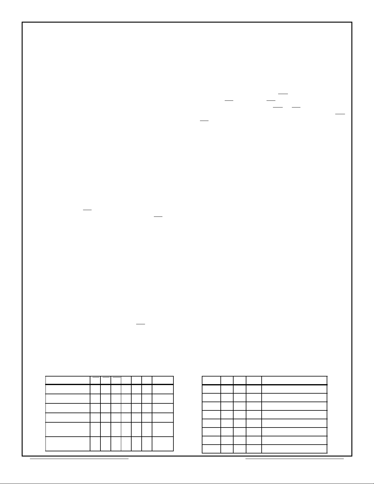
Table 1 – Bus Operations
Operation CE OE WE A0 A1 A9 I/O
READ
STANDBY
OUTPUT DISABLE
WRITE
ENABLE SECTOR
PROTECT
VERIFY SECTOR
PROTECT
Aeroflex Circuit Technology SCD1668 REV A 4/28/98 Plainview NY (516) 694-6700
L L H A
H X X X X X HIGH Z
L H H X X X HIGH Z
L H L A
L V
ID L X X VID X
L L H L H V
0 A1 A9 DOUT
0 A1 A9 DIN
ID Code
5
Table 2 – Sector Addresses Table
A16 A15 A14 Address Range
SA0 0 0 0 00000h – 03FFFh
SA1 0 0 1 04000h – 07FFFh
SA2 0 1 0 08000h – 0BFFFh
SA3 0 1 1 0C000h – 0FFFFh
SA4 1 0 0 10000h – 13FFFh
SA5 1 0 1 14000h – 17FFFh
SA6 1 1 0 18000h – 1BFFFh
SA7 1 1 1 1C000h – 1FFFFh
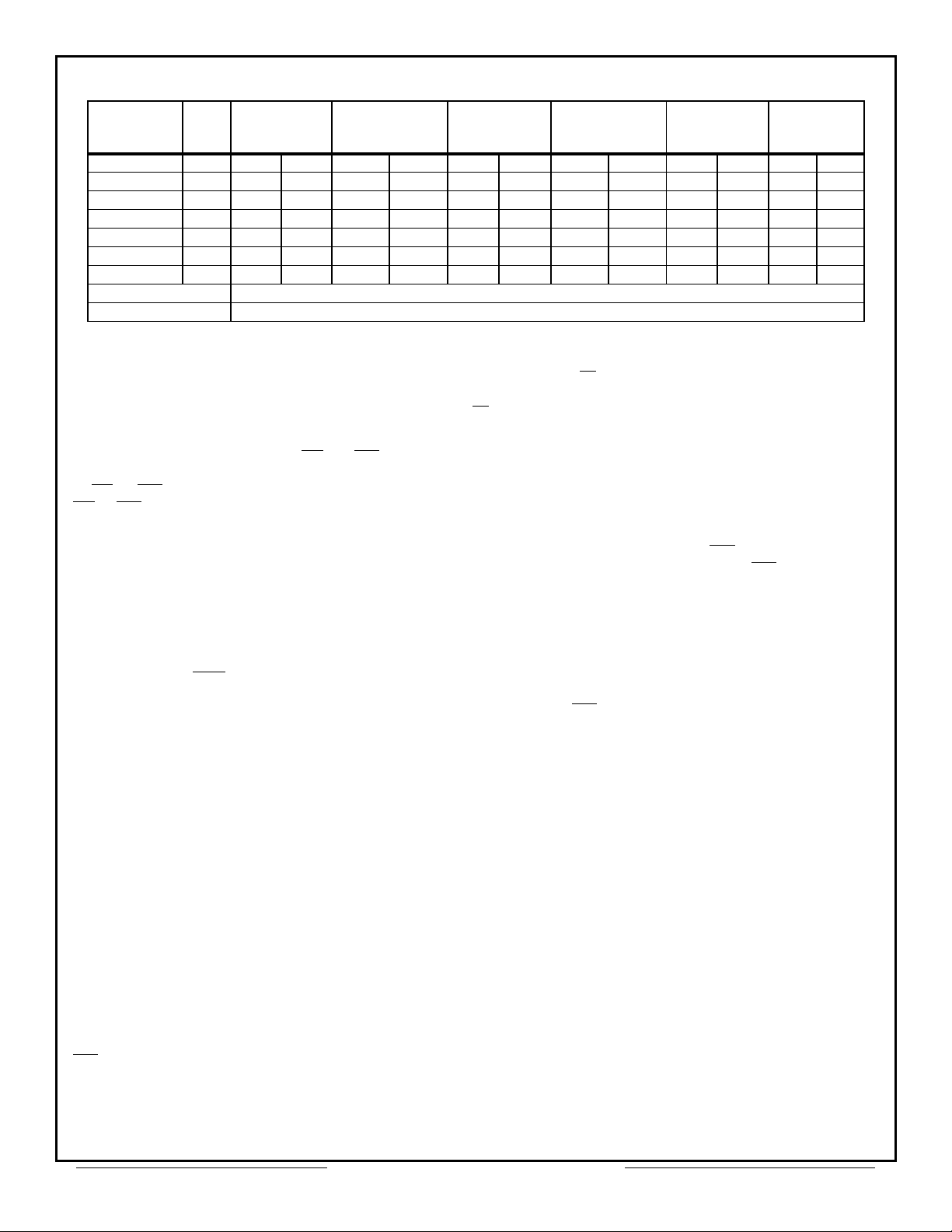
Table 3 — Commands Definitions
Command
Sequence
Required Addr Data Addr Data Addr Data Addr Data Addr Data Addr Data
Read/Reset 1 XXXH F0H
Read/Reset 4 5555H AAH 2AAAH 55H 5555H F0H RA RD
Autoselect 4 5555H AAH 2AAAH 55H 5555H 90H
Byte Program 6 5555H AAH 2AAAH 55H 5555H A0H PA PD
Chip Erase 6 5555H AAH 2AAAH 55H 5555H 80H 5555H AAH 2AAAH 55H 5555H 10H
Sector Erase 6 5555H AAH 2AAAH 55H 5555H 80H 5555H AAH 2AAAH 55H SA 30H
Sector Erase Suspend Erase can be suspended during sector erase with Address (Don’t care), Data (B0H)
Sector Erase Resume Erase can be resumed after suspend with Address (Don’t care), Data (30H)
NOTES:
1. Address bit A15, A16, A17 and A18 = X = Don't Care. Write Sequences may be initiated with A15 in either state.
2. Address bit A15, A16, A17 and A18 = X = Don't Care for all address commands except for Program Address (PA) and Sector Address (SA).
3. RA = Address of the memory location to be read
PA = Address of the memory location to be programmed. Addresses are latched on the falling edge of the WE
SA = Address of the sector to be erased. The combination of A18, A17, A16 will uniquely select any sector.
4. RD = Data read from location RA during read Operation.
PD = Data to be programmed at location PA. Data is latched on the rising edge of WE
set-up command and data write cycles. Addresses are
latched on the falling edge of CE
occurs later, while the data is latched on the rising edge
or WE whichever occurs first. The rising edge of
of CE
or WE begins programming. Upon executing the pro-
CE
gram algorithm command sequence the system is not
required to provide further controls or timings. The
device will automatically provide adequate internally
generated program pulses and verity the programmed
cell status. The automatic programming operation is
completed when the data on D
written to this bit at which time the device returns to the
read mode and addresses are no longer latched. The
device requires a valid address be supplied by the System at this time. Data
memory location which is being programmed.
Programming is allowed in any address sequence and
across sector boundaries.
Figure 3 illustrates the programming algorithm using typical command strings and bus operations.
Bus
Write
Cycles
First Bus Write
Cycle
Second Bus Write
Cycle
or WE, whichever
7 is equivalent to data
Polling must be performed at the
Third Bus Write
Cycle
.
Fourth Bus
Read/Write Cycle
pulse.
Fifth Bus Write
Cycle
Sixth Bus Write
SECTOR ERASE
Sector erase is a six bus cycle operation. There are two
"unlock" write cycles. These are followed by writing the
"setup" command. Two more "unlock" write cycles are
then followed by the sector erase command. The sector
address (any address location within the desired sector)
is latched on the falling edge of WE
(data) is latched on the rising edge of WE
100µs from the rising edge of the last sector erase command will initiate the sector erase command(s).
Multiple sectors may be erased concurrently by writing
the six bus cycle operations as described above. This
sequence is followed with writes of the sector erase command 30H to address in other sectors desired to be concurrently erased. A time-out of 100µs from the rising
edge of the WE
pulse for the last sector erase command
will initiate the sector erase. If another sector erase
command is written within the 100µs time-out window
the timer is reset. Any command other than sector erase
within the time-out window will reset the device to the
, while the command
. A time-out of
Cycle
read mode, ignoring the previous command string.
CHIP ERASE
Chip erase is a six bus cycle operation. There are two
'unlock' write cycles. These are followed by writing the
'set-up' command. Two more 'unlock' write cycles are
then followed by the chip erase command.
Chip erase does not require the user to program the
device prior to erase. Upon executing the erase algorithm (Figure 4) sequence the device automatically will
Loading the sector erase buffer may be done in any
sequence and with any number of sectors (0 to 7).
Sector erase does not require the user to program the
device prior to erase. The device automatically programs all memory locations in the sector(s) to be erased
prior to electrical erase. When erasing a sector or sectors the remaining unselected sectors are not affected.
The system is not required to provide any controls or timings during these operations.
program and verify the entire memory for an all zero data
pattern prior to electrical erase. The system is not
required to provide any controls or timings during these
operations.
The automatic erase begins on the rising edge of the last
pulse in the command sequence and terminates
WE
when the data in D7 is "1" (see Write Operation Status
section - Table 4) at which time the device returns to read
the mode. See Figures 4 and9.
Data Protection
The ACT–F512K8 is designed to offer protection against
accidental erasure or programming caused by spurious
system level singles that may exist during power transitions. During power up the device automatically resets
the internal state machine in the read mode. Also, with
Aeroflex Circuit Technology SCD1668 REV A 4/28/98 Plainview NY (516) 694-6700
6

its control register architecture, alteration of the memory
content only occurs after successful completion of specific multi-bus cycle command sequences.
The device also incorporates several features to prevent
inadvertent write cycles resulting from Vcc power-up and
power-down transitions or system noise.
LOW Vcc WRITE INHIBIT
To avoid initiation of a write cycle during Vcc power-up
and power-down, a write cycle is locked out for V
than 3.2V (typically 3.7V). If V
CC <VLKO, the command
CC less
register is disabled and all internal program/erase circuits are disabled. Under this condition the device will
reset to read mode. Subsequent writes will be ignored
until the Vcc level is greater than V
LKO. It is the users
responsibility to ensure that the control pins are logically
correct to prevent unintentional writes when Vcc is above
3.2V.
WRITE PULSE GLITCH PROTECTION
Noise pulses of less than 5ns (typical) on OE, CE or WE
will not initiate a write cycle.
LOGICAL INHIBIT
Writing is inhibited by holding anyone of OE = VIL, CE =
IH or WE = VIH. To initiate a write cycle CE and WE
V
must be logical zero while OE is a logical one.
POWER-UP WRITE INHIBIT
Power-up of the device with WE = CE = VIL and OE =
IH will not accept commands on the rising edge ofWE.
V
The internal state machine is automatically reset to the
read mode on power-up.
Write Operation Status
D7
DATA POLLING
The ACT-F512K8 features Data Polling as a method to
indicate to the host that the internal algorithms are in
progress or completed. During the program algorithm, an
attempt to read the device will produce compliment data
of the data last written to D
an attempt to read the device will produce a "0" at the D
Output. Upon completion of the erase algorithm an
attempt to read the device will produce a "1" at the D
Output.
For chip Erase, the Data
edge of the sixth WE
sequence. For sector erase, the Data
the last rising edge of the sector erase WE
polling must be performed at a sector address within any
of the sectors being erased and not a protected sector.
Otherwise, the status may not be valid. Once the algo-
7. During the erase algorithm,
Polling is valid after the rising
pulse in the six write pulse
Polling is valid after
pulse. Data
rithm operation is close to being completed, data pins
(D
7) change asynchronously while the output enable
) is asserted low. This means that the device is driv-
(OE
ing status information on D
7 at one instance of time and
then that byte's valid data at the next instant of time.
Depending on when the system samples the D
it may read the status or valid data. Even if the device
has completed internal algorithm operation and D
valid data, the data outputs on D
invalid. The valid data on D0-D
cessive read attempts. The Data
0 - D6 may be still
7 will be read on the suc-
Polling feature is only
active during the programming algorithm, erase algorithm, or sector erase time-out.
See Figures 6 and 10 for the Data Polling specifications.
D6
TOGGLE BIT
The ACT–F512K8 also features the "Toggle Bit" as a
method to indicate to the host system that algorithms are
in progress or completed.
During a program or erase algorithm cycle, successive
attempts to read data from the device will result in D
toggling between one and zero. Once the program or
erase algorithm cycle is completed, D
6 Will stop toggling
and valid data will be read on successive attempts. During programming the Toggle Bit is valid after the rising
edge of the fourth WE
pulse in the four write pulse
sequence. For chip erase the Toggle Bit is valid after the
rising edge of the sixth
WE pulse in the six write pulse
sequence. For Sector erase, the Toggle Bit is valid after
the last rising edge of the sector erase
WE pulse. The
Toggle Bit is active during the sector time out.
See Figure 1 and 5.
D5
EXCEEDED TIMING LIMITS
D5 will indicate if the program or erase time has
exceeded the specified limits. Under these conditions
5 will produce a "1". The Program or erase cycle was
D
not successfully completed. Data
Polling is the only
operation function of the device under this condition.
The CE
circuit will partially power down the device under
these conditions by approximately 2 mA. The OE
pins will control the output disable functions as
WE
shown in Table 1. To reset the device, write the reset
command sequence to the device. This allows the system to continue to use the other active sectors in the
device.
7
7
D3
SECTOR ERASE TIMER
After the completion of the initial sector erase command
sequence the sector erase time-out will begin. D
remain low until the time-out is complete. Data Polling
and Toggle Bit are valid after the initial sector erase command sequence.
7 Output,
7 has a
6
and
3 will
Aeroflex Circuit Technology SCD1668 REV A 4/28/98 Plainview NY (516) 694-6700
7
 Loading...