

ACT ACT-7000SC-225F17M, ACT-7000SC-210F17T, ACT-7000SC-200F17C, ACT-7000SC Datasheet

ACT 7000SC
64-Bit Superscaler Microprocessor
Features
■
Full militarized QED RM7000 microprocessor
■
Dual Issue symmetric superscalar microprocessor with
instruction prefetch optimized for system level
price/performance
●
150, 200, 210, 225 MHz operating frequency
Consult Factory for latest speeds
●
MIPS IV Superset Instruction Set Architecture
■
High performance interface (RM52xx compatible)
●
600 MB per second peak throughput
●
75 MHz max. freq., multiplexed address/data
●
Supports 1/2 clock multipliers (2, 2.5, 3, 3.5, 4, 4.5, 5, 6, 7, 8, 9)
●
IEEE 1149.1 JTAG (TAP) boundary scan
■
Integrated primary and secondary caches - all are 4-way set
associative with 32 byte line size
●
16KB instruction
●
16KB data: non-blocking and write-back or write-through
●
256KB on-chip secondary: unified, non-blocking, block writeback
■
MIPS IV instruction set
●
Data PREFETCH instruction allows the processor to overlap cache
miss latency and instruction execution
●
Floating point combined multiply-add instruction increases
performance in signal processing and graphics applications
●
Conditional moves reduce branch frequency
●
Index address modes (register + register)
■
Embedded supply de-coupling capacitors and additional PLL
filter components
■
Integrated memory management unit (ACT52xx compatible)
●
Fully associative joint TLB (shared by I and D translations)
●
48 dual entries map 96 pages
●
4 entry DTLB and 4 entry ITLB
●
Variable page size (4KB to 16MB in 4x increments)
■
Embedded application enhancements
●
Specialized DSP integer Multiply-Accumulate instruction,
(MAD/MADU) and three-operand multiply instruction (MUL/U)
●
Per line cache locking in primaries and secondary
●
Bypass secondary cache option
●
I&D Test/Break-point (Watch) registers for emulation & debug
●
Performance counter for system and software tuning & debug
●
Ten fully prioritized vectored interrupts - 6 external, 2 internal, 2
software
●
Fast Hit-Writeback-Invalidate and Hit-Invalidate cache operations
for efficient cache management
■
High-performance floating point unit - 600 M FLOPS
maximum
●
Single cycle repeat rate for common single-precision operations
and some double-precision operations
●
Single cycle repeat rate for single-precision combined multiplyadd operations
●
Two cycle repeat rate for double-precision multiply and
double-precision combined multiply-add operations
■
Fully static CMOS design with dynamic power down logic
●
Standby reduced power mode with WAIT instruction
●
4 watts typical @ 2.5V Int., 3.3V I/O, 200MHz
■
208-lead CQFP, cavity-up package (F17)
■
208-lead CQFP, inverted footprint (F24), with the same pin
rotation as the commercial QED RM5261
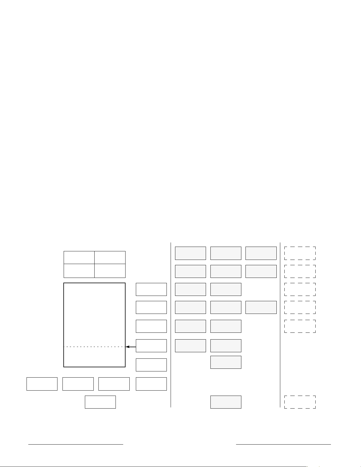
BLOCK DIAGRAM
Store Buffer
Packer / Unpacker
MultAdd, Add, Sub,
Secondary Tags
Set A
Primary Data Cache
4 - Way Set Associative
Write Buffer
Read Buffer
D Bus
Floating-Point
Load /Align
Floating-Point
Register File
Comparator
Floating-Point
Cvt, Div, Sqrt
Multiplier Array
On -Chip 256K Byte Secondary Cache, 4 -Way Set Associative
Secondary Tags
Set B
System /Memory
Floating -Point Control
DTag
DTLB
Pad Buffer
Address Buffer
Joint TLB
Coprocessor 0
Control
PC Incrementer
Branch PC Adder
ITLB Virtuals
Program Counter
Secondary Tags
ITag
ITLB
DVA
IVA
Set C
Primar y Instruction Cache
F-Pipe Bus
Load Aligner
Integer Register File
M Pipe F Pipe
Adder
StAin/Sh Shifter
FA Bus
DTLB Virtuals
Secondary Tags
Set D
4 -Way Set Associative
A/D Bus
Prefetch Buffer
Instruction Dispatch Unit
F Pipe Register
M Pipe Register
Int Mult. Div. MaddPLL/Clocks
Pad Bus
M-Pipe Bus
Adder
LogicalsLogicals
Integer Control
eroflex Circuit
Technology
– MIPS RISC Microprocessors © SCD7000SC REV B 7/30/01
DESCRIPTION
The ACT 7000SC is a highly integrated symmetric
superscalar microprocessor capable of issuing two
instructions each processor cycle. It has two high
performance 64-bit integer units as well as a high
throughput, fully pipelined 64-bit floating point unit. To
keep its multiple execution units running efficiently,
the ACT 7000SC integrates not only 16KB 4-way set
associative instruction and data caches but backs
them up with an integrated 256KB 4-way set
associative secondary as well. For maximum
efficiency, the data and secondary caches are
writeback and nonblocking. A RM52XX family
compatible, operating system friendly memory
management unit with a 64 / 48-entry fully associative
TLB and a high-performance 64-bit system interface
supporting hardware prioritized and vectored
interrupts round out the main features of the
processor.
The ACT 7000SC is ideally suited for highend
embedded control applications such as
internetworking, high performance image
manipulation, high speed printing, and 3-D
visualization.
HARDWARE OVERVIEW
The ACT 7000SC offers a high-level of integration
targeted at high-performance embedded
applications. The key elements of the ACT 7000SC
are briefly described below.
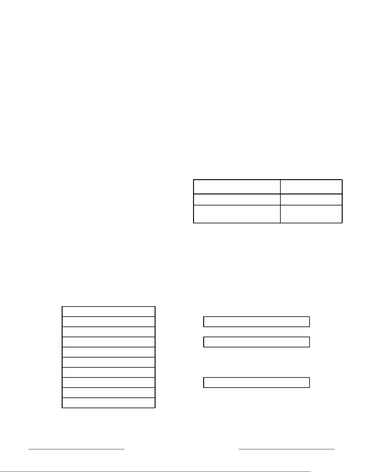
CPU Registers
Like all MIPS ISA processors, the ACT 7000SC
CPU has a simple, clean user visible state consisting
of 32 general purpose registers, or GPR’s, two special
purpose registers for integer multiplication and
division, and a program counter; there are no
condition code bits. Figure 1 shows the user visible
state.
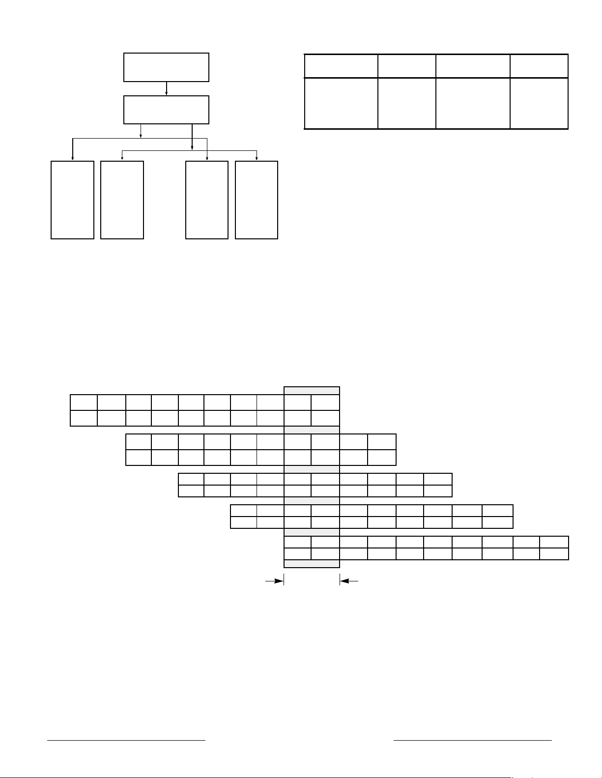
Superscalar Dispatch
The ACT 7000SC has an efficient symmetric
superscalar dispatch unit which allows it to issue up to
two instructions per cycle. For purposes of instruction
issue, the ACT 7000SC defines four classes of
instructions: integer, load/store, branches, and
floating-point. There are two logical pipelines, the
function
, or F, pipeline and the
memory
, or M,
pipeline. Note however that the M pipe can execute
integer as well as memory type instructions.
Table 1 – Instruction Issue Rules
F Pipe M Pipe
one of: one of:
integer, branch, floating-point,
integer mul, div
Figure 2 is a simplification of the pipeline section
and illustrates the basics of the instruction issue
mechanism.
integer, load/store
General Purpose Registers
63 0 Multiply/Divide Registers
063
r1 HI
r2 63
•LO
•
• Program Counter
•63
r29 PC
r30
r31
0
0
0
Figure 1 – CP0 Registers
Aeroflex Circuit Technology SCD7000SC REV B 7/30/01 Plainview NY (516) 694-6700
2
.
Table 2 – Dual Issue Instruction Classes
Instruction
Cache
Dispatch
Unit
F Pipe IBus
M Pipe IBus
FP
F Pipe
FP
M Pipe
Integer
F Pipe
Integer
M Pipe
Figure 2 – Instruction Issue Paradigm
The figure illustrates that one F pipe instruction and
one M pipe instruction can be issued concurrently but
that two M pipe or two F pipe instructions cannot be
issued. Table 2 specifies more completely the
instructions within each class.
integer load/store floating-point branch
add, sub, or, xor,
shift, etc.
lw, sw, ld, sd,
ldc1, sdc1,
mov, movc,
fmov, etc.
fadd, fsub, fmult,
fmadd, fdiv, fcmp,
fsqrt, etc.
beq, bne,
bCzT, bCzF, j,
etc.
The symmetric superscalar capability of the ACT
7000SC, in combination with its low latency integer
execution units and high-throughput fully pipelined
floating-point execution unit, provides unparalleled
price/performance in computational intensive
embedded applications.
Pipeline
The logical length of both the F and M pipelines is
five stages with state committing in the register write,
or W, pipe stage. The physical length of the
floating-point execution pipeline is actually seven
stages but this is completely transparent to the user.
Figure 3 shows instruction execution within the
ACT 7000SC when instructions are issuing
simultaneously down both pipelines. As illustrated in
the figure, up to ten instructions can be executing
simultaneously. This figure presents a somewhat
simplistic view of the processors operation however
since the out-of-order completion of loads, stores, and
I0 1l 2l 1R 2R 1A 2A 1D 2D 1W 2W
I1 1l 2l 1R 2R 1A 2A 1D 2D 1W 2W
I2 1l 2l 1R 2R 1A 2A 1D 2D 1W 2W
I3 1l 2l 1R 2R 1A 2A 1D 2D 1W 2W
I4 1l 2l 1R 2R 1A 2A 1D 2D 1W 2W
I5 1l 2l 1R 2R 1A 2A 1D 2D 1W 2W
I6 1l 2l 1R 2R 1A 2A 1D 2D 1W 2W
I7 1l 2l 1R 2R 1A 2A 1D 2D 1W 2W
I8 1l 2l 1R 2R 1A 2A 1D 2D 1W 2W
I9 1l 2l 1R 2R 1A 2A 1D 2D 1W 2W
one cycle
Instruction cache access
1I-1R:
Instruction virtual to physical address translation
2I:
Register file read, Bypass calculation, Instruction decode, Branch address calculation
2R:
Issue or slip decision, Branch decision
1A:
Data vir tual address calculation
1A:
Integer add, logical, shift
1A-2A:
Store Align
2A:
Data cache access and load align
2A-2D:
Data virtual to physical address translation
1D:
Register file write
2W:
Figure 3 – Pipeline
Aeroflex Circuit Technology SCD7000SC REV B 7/30/01 Plainview NY (516) 694-6700
3
long latency floating-point operations can result in
Table 3 – ALU Operations
there being even more instructions in process than
what is shown.
Note that instruction dependencies, resource
conflicts, and branches result in some of the
instruction slots being occupied by NOPs.
Integer Unit
Like the ACT 52xx family, the ACT 7000SC
Unit F Pipe M Pipe
Adder add, sub add, sub, data address
add
Logic logic, moves, zero shifts
(nop)
Shifter non zero shift non zero shift, store
logic, moves, zero shifts
(nop)
align
implements the MIPS IV Instruction Set Architecture,
and is therefore fully upward compatible with
applications that run on processors such as the
R4650 and R4700 that implement the earlier
generation MIPS III Instruction Set Architecture.
Additionally, the ACT 7000SC includes two
implementation specific instructions not found in the
baseline MIPS IV ISA, but that are useful in the
Integer Multiply/Divide
The ACT 7000SC has a single dedicated integer
multiply/divide unit optimized for high-speed multiply
and multiply-accumulate operations. The
multiply/divide unit resides in the F type execution
unit. Table 4 shows the performance of the
multiply/divide unit on each operation.
embedded market place. Described in detail in a later
section of this datasheet, these instructions are
integer multiply-accumulate and three-operand
integer multiply.
The ACT 7000SC integer unit includes thirty-two
general purpose 64-bit registers, the HI/LO result
registers for the two-Pipeline operand integer
multiply/divide operations, and the program counter,
or PC. There are two separate execution units, one of
which can execute function, or F, type instructions
and one which can execute memory, or M, type
instructions. See above for a description of the
instruction types and the issue rules. As a special
case, integer multiply/divide instructions as well as
their corresponding MFHi and MFLo instructions can
Table 4 – Integer Multiply/ Divide Operations
Operand
Opcode
MULT/U,
MAD/U
MUL 16 bit 4 3 2
DMULT,
DMULTU
DIV, DIVD any 36 36 0
DDIV,
DDIVU
Size Latency
16 bit 4 3 0
32 bit 5 4 0
32 bit 5 4 3
any980
any 68 68 0
Repeat
Rate
Cycles
only be executed in the F type execution unit. Within
each execution unit the operational characteristics
are the same as on previous QED designs with single
cycle ALU operations (add, sub, logical, shift), one
cycle load delay, and an autonomous multiply/divide
unit.
The baseline MIPS IV ISA specifies that the results
of a multiply or divide operation be placed in the Hi
and Lo registers. These values can then be
transferred to the general purpose register file using
the Move-from-Hi and Move-from-Lo (MFHI/MFLO)
instructions.
Register File
The ACT 7000SC has thirty-two general purpose
registers with register location (r0) hard wired to zero
value. These registers are used for scalar integer
operations and address calculation. In order to
service the two integer execution units, the register
file has four read ports and two write ports and is fully
bypassed both within and between the two execution
units to minimize operation latency in the pipeline.
In addition to the baseline MIPS IV integer multiply
instructions, the ACT 7000SC also implements the
3-operand multiply instruction, MUL. This instruction
specifies that the multiply result go directly to the
integer register file rather than the Lo register. The
portion of the multiply that would have normally gone
into the Hi register is discarded. For applications
where it is known that the upper half of the multiply
result is not required, using the MUL instruction
eliminates the necessity of executing an explicit
ALU
The ACT 7000SC has two complete integer ALU’s
each consisting of an integer adder/subtractor, a logic
unit, and a shifter. Table 3 shows the functions
performed by the ALU’s for each execution unit. Each
of these units is optimized to perform all operations in
a single processor cycle.
MFLO instruction.
Also included in the ACT 7000SC are the
multiply-add instructions MAD/MADU. This
instruction multiplies two operands and adds the
resulting product to the current contents of the Hi and
Lo registers. The multiply-accumulate operation is the
core primitive of almost all signal processing
algorithms allowing the ACT 7000SC to eliminate the
need for a separate DSP engine in many embedded
applications.
Aeroflex Circuit Technology SCD7000SC REV B 7/30/01 Plainview NY (516) 694-6700
4
Stall
By pipelining the multiply-accumulate function and
dynamically determining the size of the input
Table 5 – Floating Point Latencies and
Repeat Rates
operands, the ACT 7000SC is able to maximize
throughput while still using an area efficient
implementation.
Floating-Point Coprocessor
The ACT 7000SC incorporates a high-performance
fully pipe-lined floating-point coprocessor which
includes a floating-point register file and autonomous
execution units for multiply/ add/convert and
divide/square root. The floating-point coprocessor is a
tightly coupled co-execution unit, decoding and
executing instructions in parallel with, and in the case
of floating-point loads and stores, in cooperation with
the M pipe of the integer unit. As described earlier, the
superscalar capabilities of the ACT 7000SC allow
floating-point computation instructions to issue
concurrently with integer instructions.
Floating-Point Unit
The ACT 7000SC floating-point execution unit
supports single and double precision arithmetic, as
specified in the IEEE Standard 754. The execution
unit is broken into a separate divide/square root unit
and a pipelined multiply/add unit. Overlap of
divide/square root and multiply/add is supported.
The ACT 7000SC maintains fully precise
floating-point exceptions while allowing both
overlapped and pipelined operations. Precise
exceptions are extremely important in object-oriented
programming environments and highly desirable for
Operation
fadd 4 1
fsub 4 1
fmult 4/5 1/2
fmadd 4/5 1/2
fmsub 4/5 1/2
fdiv 21/36 19/34
fsqrt 21/36 19/34
frecip 21/36 19/34
frsqrt 38/68 36/66
fcvt.s.d 4 1
fcvt.s.w 6 3
fcvt.s.l 6 3
fcvt.d.s 4 1
fcvt.d.w 4 1
fcvt.d.l 4 1
fcvt.w.s 4 1
fcvt.w.d 4 1
fcvt.l.s 4 1
fcvt.l.d 4 1
fcmp 1 1
fmov, fmovc 1 1
fabs, fneg 1 1
Latency
single/double
Repeat Rate
single/double
debugging in any environment.
The floating-point unit’s operation set includes
floating-point add, subtract, multiply, multiply-add,
divide, square root, reciprocal, reciprocal square root,
conditional moves, conversion between fixed-point
and floating-point format, conversion between
floating-point formats, and floating-point compare.
Table 5 gives the latencies of the floating-point
instructions in internal processor cycles.
To support superscalar operations, the FGR has
four read ports and two write ports, and is fully
bypassed to minimize operation latency in the
pipeline. Three of the read ports and one write port
are used to support the combined multiply-add
instruction while the fourth read and second write port
allows a concurrent floating-point load or store and
conditional moves.
System Control Coprocessor (CP0)
Floating-Point General Register File
The floating-point general register file, FGR, is
made up of thirty-two 64-bit registers. With the
floating-point load and store double instructions,
LDC1 and SDC1, the floating-point unit can take
advantage of the 64-bit wide data cache and issue a
floating-point coprocessor load or store double-word
instruction in every cycle.
The floating-point control register file contains two
registers; one for determining configuration and
revision information for the coprocessor and one for
control and status information. These registers are
primarily used for diagnostic software, exception
handling, state saving and restoring, and control of
rounding modes.
Aeroflex Circuit Technology SCD7000SC REV B 7/30/01 Plainview NY (516) 694-6700
The system control coprocessor (CP0) in the MIPS
architecture is responsible for the virtual memory
sub-system, the exception control system, and the
diagnostics capability of the processor. In the MIPS
architecture, the system control coprocessor (and
thus the kernel software) is implementation
dependent. For memory management, the ACT
7000SC CP0 is logically identical to that of the
RM5200 Family and R5000. For interrupt exceptions
and diagnostics, the ACT 7000SC is a superset of the
RM5200 Family and R5000 implementing additional
features described later in the sections on Interrupts,
the Test/Breakpoint facility, and the Performance
Counter facility.
The memory management unit controls the virtual
memory system page mapping. It consists of an
instruction address translation buffer, or ITLB, a data
5
address translation buffer, or DTLB, a Joint TLB, or
JTLB, and coprocessor registers used by the virtual
memory mapping sub-system.
System Control Coprocessor Registers
The ACT 7000SC incorporates all system control
coprocessor (CP0) registers internally. These
registers provide the path through which the virtual
memory system’s page mapping is examined and
modified, exceptions are handled, and operating
modes are controlled (kernel vs. user mode,
interrupts enabled or disabled, cache features). In
addition, the ACT 7000SC includes registers to
implement a real-time cycle counting facility, to aid in
cache and system diagnostics, and to assist in data
error detection.
To support the non-blocking caches and enhanced
interrupt handling capabilities of the ACT 7000SC,
both the data and control register spaces of CP0 are
supported by the ACT 7000SC. In the data register
space, that is the space accessed using the MFC0
and MTC0 instructions, the ACT 7000SC supports the
same registers as found in the RM5200, R4000 and
R5000 families. In the control space, that is the space
accessed by the previously unused CTC0 and CFC0
instructions, the ACT 7000SC supports five new
registers. The first three of these new 32-bit registers
support the enhanced interrupt handling capabilities
and are the Interrupt Control, Interrupt Priority Level
Lo (IPLLO), and Interrupt Priority Level Hi (IPLHI)
registers. These registers are described further in the
section on interrupt handling. The other two registers,
Imprecise Error 1
and
Imprecise Error 2
, have been
added to help diagnose bus errors which occur on
non-blocking memory references.
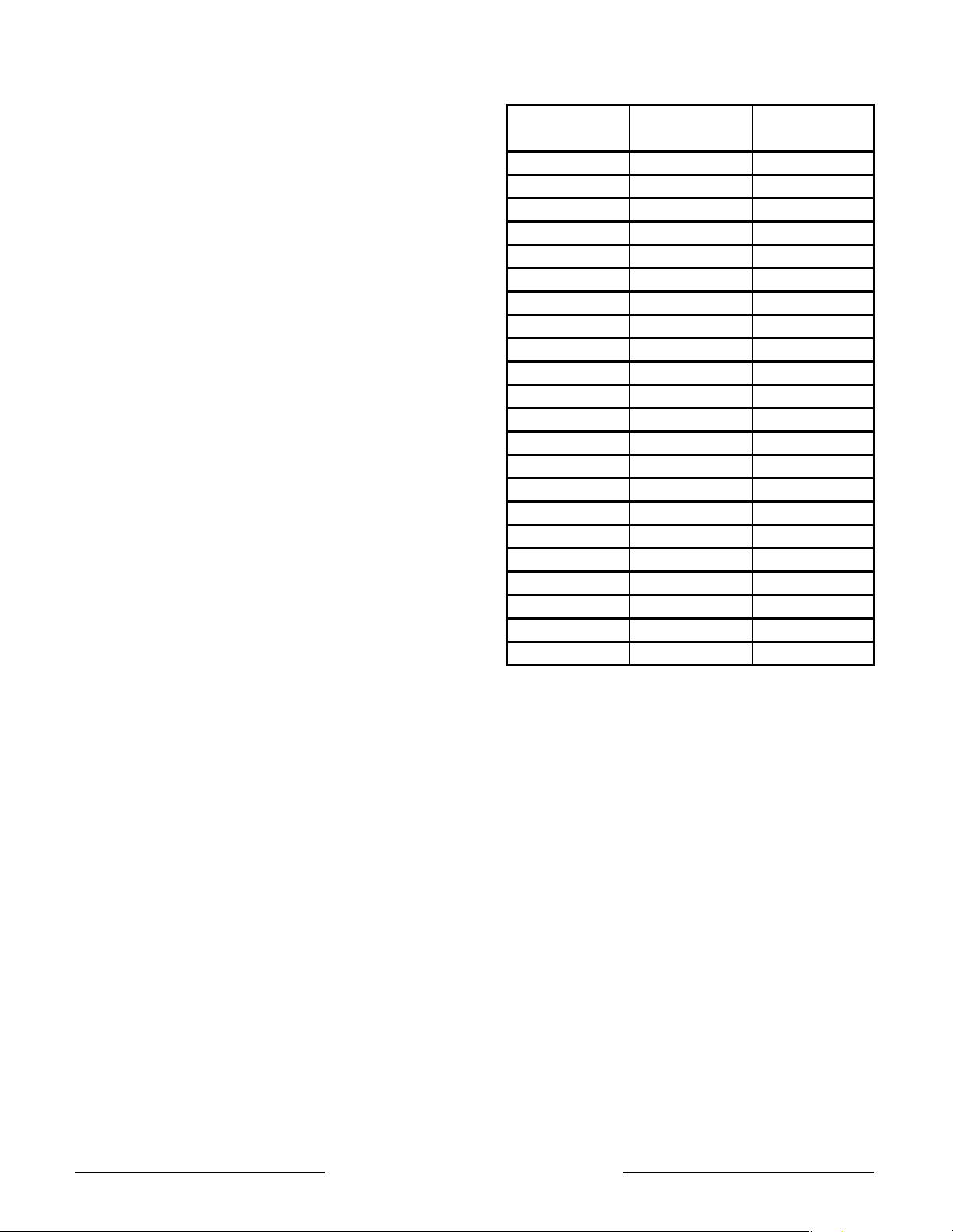
Figure 4 shows the CP0 registers.
Virtual to Physical Address Mapping
The ACT 7000SC provides three modes of virtual
addressing:
• user mode
• supervisor mode
• kernel mode
This mechanism is available to system software to
provide a secure environment for user processes. Bits
in the CP0 Status register determine which virtual
addressing mode is used. In the user mode, the ACT
7000SC provides a single, uniform virtual address
space of 256GB (2GB in 32-bit mode).
When operating in the kernel mode, four distinct
virtual address spaces, totalling 1024GB (4GB in
32-bit mode), are simultaneously available and are
differentiated by the high-order bits of the virtual
address.
The ACT 7000SC processor also supports a
supervisor mode in which the virtual address space is
256.5GB (2.5GB in 32-bit mode), divided into three
regions based on the high-order bits of the virtual
address. Figure 5 shows the address space layout for
32-bit operation.
LLAddr
17*
PageMask
5*
EntryHi
10*
47
(entries protected
from TLBWR)
0
TagLo
28*
EntryLo0
2*
EntryLo1
3*
TLB
TagHi
29*
Used for memory
management
Context
Info
7*
Index
0*
Random
1*
Wired
6*
PRid
15*
Config
16*
* Registered number
Status
Watch2
4*
Count
9*
12*
EPC
14*
19*
ECC
26*
BadVAddr
8*
Compare
11*
Cause
13*
Watch1
18*
Xcontext
20*
CacheErr
27*
ErrorEPC
30*
Used for exception
processing
Perf Counter
25*
Perf Ctr Cntrl
22*
Watch Mask
24*
IPLLO
18*
IPLHI
19*
IntControl
20*
Imp Error 1
26*
Imp Error 2
27*
Control Space Registers
Figure 4 – CP0 Registers
Aeroflex Circuit Technology SCD7000SC REV B 7/30/01 Plainview NY (516) 694-6700
6
Figure 5 – Kernel Mode Virtual Addressing
(32-bit mode)
is loaded with the desired page size of a mapping,
and that size is stored into the TLB along with the
virtual address when a new entry is written. Thus,
0xFFFFFFFF Kernel virtual address space
(kseg3)
Mapped, 0.5GB
0xE0000000
0xDFFFFFFF Supervisor virtual address space
(ksseg)
Mapped, 0.5GB
0xC0000000
0xBFFFFFFF Uncached kernel physical address space
(kseg1)
Unmapped, 0.5GB
0xA0000000
0x9FFFFFFF Cached kernel physical address space
(kseg0)
Unmapped, 0.5GB
0x80000000
0x7FFFFFFF User virtual address space
(kuseg)
Mapped, 2.0GB
operating systems can create special purpose maps;
for example, a typical frame buffer can be memory
mapped using only one TLB entry.
The second mechanism controls the replacement
algorithm when a TLB miss occurs. The ACT 7000SC
provides a random replacement algorithm to select a
TLB entry to be written with a new mapping; however,
the processor also provides a mechanism whereby a
system specific number of mappings can be locked
into the TLB, thereby avoiding random replacement.
This mechanism allows the operating system to
guarantee that certain pages are always mapped for
performance reasons and for deadlock avoidance.
This mechanism also facilitates the design of
real-time systems by allowing deterministic access to
critical software.
The JTLB also contains information that controls
the cache coherency protocol for each page.
Specifically, each page has attribute bits to determine
whether the coherency algorithm is: uncached,
write-back, write-through with write-allocate,
write-through without write-allocate, write-back with
secondary bypass. Note that both of the write-through
protocols bypass the secondary cache since it does
not support writes of less than a complete cache line.
These protocols are used for both code and data on
the ACT 7000SC with data using write-back or
write-through depending on the application. The
write-through modes support the same efficient frame
buffer handling as the RM5200 Family, R4700 and
R5000.
0x00000000
Instruction TLB
The ACT 7000SC uses a 4-entry instruction TLB
When the ACT 7000SC is configured for 64-bit
addressing, the virtual address space layout is an
upward compatible extension of the 32-bit virtual
address space layout.
Joint TLB
For fast virtual-to-physical address translation, the
ACT 7000SC uses a large, fully associative TLB that
maps virtual pages to their corresponding physical
addresses. As indicated by its name, the joint TLB
(JTLB) is used for both instruction and data
translations. The JTLB is organized as pairs of
even/odd entries, and maps a virtual address and
address space identifier into the large, 64GB physical
address space. By default, the JTLB is configured as
48 pairs of even/odd entries. The 64 even/odd entry
optional configuration is set at boot time.
Two mechanisms are provided to assist in
controlling the amount of mapped space, and the
replacement characteristics of various memory
regions. First, the page size can be configured, on a
per-entry basis, to use page sizes in the range of 4KB
to 16MB (in 4X multiples). A CP0 register, PageMask,
Aeroflex Circuit Technology SCD7000SC REV B 7/30/01 Plainview NY (516) 694-6700
(ITLB) to minimize contention for the JTLB, to
eliminate the critical path of translating through a
large associative array, and to save power. Each ITLB
entry maps a 4KB page. The ITLB improves
performance by allowing instruction address
translation to occur in parallel with data address
translation. When a miss occurs on an instruction
address translation by the ITLB, the least-recently
used ITLB entry is filled from the JTLB. The operation
of the ITLB is completely transparent to the user.
Data TLB
The ACT 7000SC uses a 4-entry data TLB (DTLB)
for the same reasons cited above for the ITLB. Each
DTLB entry maps a 4KB page. The DTLB improves
performance by allowing data address translation to
occur in parallel with instruction address translation.
When a miss occurs on a data address translation by
the DTLB, the DTLB is filled from the JTLB. The DTLB
refill is pseudo-LRU: the least recently used entry of
the least recently used pair of entries is filled. The
operation of the DTLB is completely transparent to the
user.
7

Cache Memory
In order to keep the ACT 7000SC’s superscalar
pipeline full and operating efficiently, the ACT
7000SC has integrated primary instruction and data
caches with single cycle access as well as a large
unified secondary cache with a three cycle miss
penalty from the primaries. Each primary cache has a
64-bit read path, a 128-bit write path, and both caches
can be accessed simultaneously. The primary caches
provide the integer and floating-point units with an
aggregate band-width of 3.6 GB per second at an
internal clock frequency of 225 MHz. During an
instruction or data primary cache refill, the secondary
cache can provide a 64-bit datum every cycle
following the initial three cycle latency for a peak
bandwidth of 2.4 GB per second.
Instruction Cache
The ACT 7000SC has an integrated 16KB,
four-way set associative instruction cache and, even
though instruction address translation is done in
parallel with the cache access, the combination of
4-way set associativity and 16KB size results in a
cache which is virtually indexed and physically
tagged. Since the effective physical index eliminates
the potential for virtual aliases in the cache, it is
possible that some operating system code can be
simplified as compared with the RM5200 Family,
R5000 and R4000 class processors.
The data array portion of the instruction cache is 64
bits wide and protected by word parity while the tag
array holds a 24-bit physical address, 14
housekeeping bits, a valid bit, and a single bit of parity
protection.
By accessing 64 bits per cycle, the instruction
cache is able to supply two instructions per cycle to
the superscalar dispatch unit. For signal processing,
graphics, and other numerical code sequences where
a floating-point load or store and a floating-point
computation instruction are being issued together in a
loop, the entire bandwidth available from the
instruction cache will be consumed by instruction
issue. For typical integer code mixes, where
instruction dependencies and other resource
constraints restrict the achievable parallelism, the
extra instruction cache bandwidth is used to fetch
both the taken and non-taken branch paths to
minimize the overall penalty for branches. A 32-byte
(eight instruction) line size is used to maximize the
communication efficiency between the instruction
cache and the secondary cache, or memory system.
The ACT 7000SC is the first MIPS RISC
microprocessor to support cache locking on a per line
basis. The contents of each line of the cache can be
locked by setting a bit in the Tag. Locking the line
prevents its contents from being overwritten by a
subsequent cache miss. Refill will occur only into
unlocked cache lines. This mechanism allows the
programmer to lock critical code into the cache
locked code sequence.
Data Cache
The ACT 7000SC has an integrated 16KB,
four-way set associative data cache, and even though
data address translation is done in parallel with the
cache access, the combination of 4-way set
associativity and 16KB size results in a cache which
is physically indexed and physically tagged. Since the
effective physical index eliminates the potential for
virtual aliases in the cache, it is possible that some
operating system code can be simplified compared to
the RM5200 Family, R5000 and R4000 class
processors. The data cache is non-blocking; that is, a
miss in the data cache will not necessarily stall the
processor pipeline. As long as no instruction is
encountered which is dependent on the data
reference which caused the miss, the pipeline will
continue to advance. Once there are two cache
misses outstanding, the processor will stall if it
encounters another load or store instruction. A
32-byte (eight word) line size is used to maximize the
communication efficiency between the data cache
and the secondary cache or memory system. The
data array portion of the data cache is 64 bits wide
and protected by byte parity while the tag array holds
a 24-bit physical address, 3 housekeeping bits, a two
bit cache state field, and has two bits of parity
protection. The normal write policy is write-back,
which means that a store to a cache line does not
immediately cause memory to be updated. This
increases system performance by reducing bus traffic
and eliminating the bottleneck of waiting for each
store operation to finish before issuing a subsequent
memory operation. Software can, however, select
write-through on a per-page basis when appropriate,
such as for frame buffers. Cache protocols supported
for the data cache are:
1. Uncached. Reads to addresses in a memory
area identified as uncached will not access the
cache. Writes to such addresses will be written
directly to main memory without updating the
cache.
2. Write-back. Loads and instruction fetches will
first search the cache, reading the next memory
hierarchy level only if the desired data is not
cache resident. On data store operations, the
cache is first searched to determine if the target
address is cache resident. If it is resident, the
cache contents will be updated, and the cache
line marked for later write-back. If the cache
lookup misses, the target line is first brought into
the cache and then the write is performed as
above.
3. Write-through with write allocate. Loads and
instruction fetches will first search the cache,
reading from memory only if the desired data is
not cache resident; write-through data is never
cached in the secondary cache. On data store
thereby guaranteeing deterministic behavior for the
Aeroflex Circuit Technology SCD7000SC REV B 7/30/01 Plainview NY (516) 694-6700
8
 Loading...