

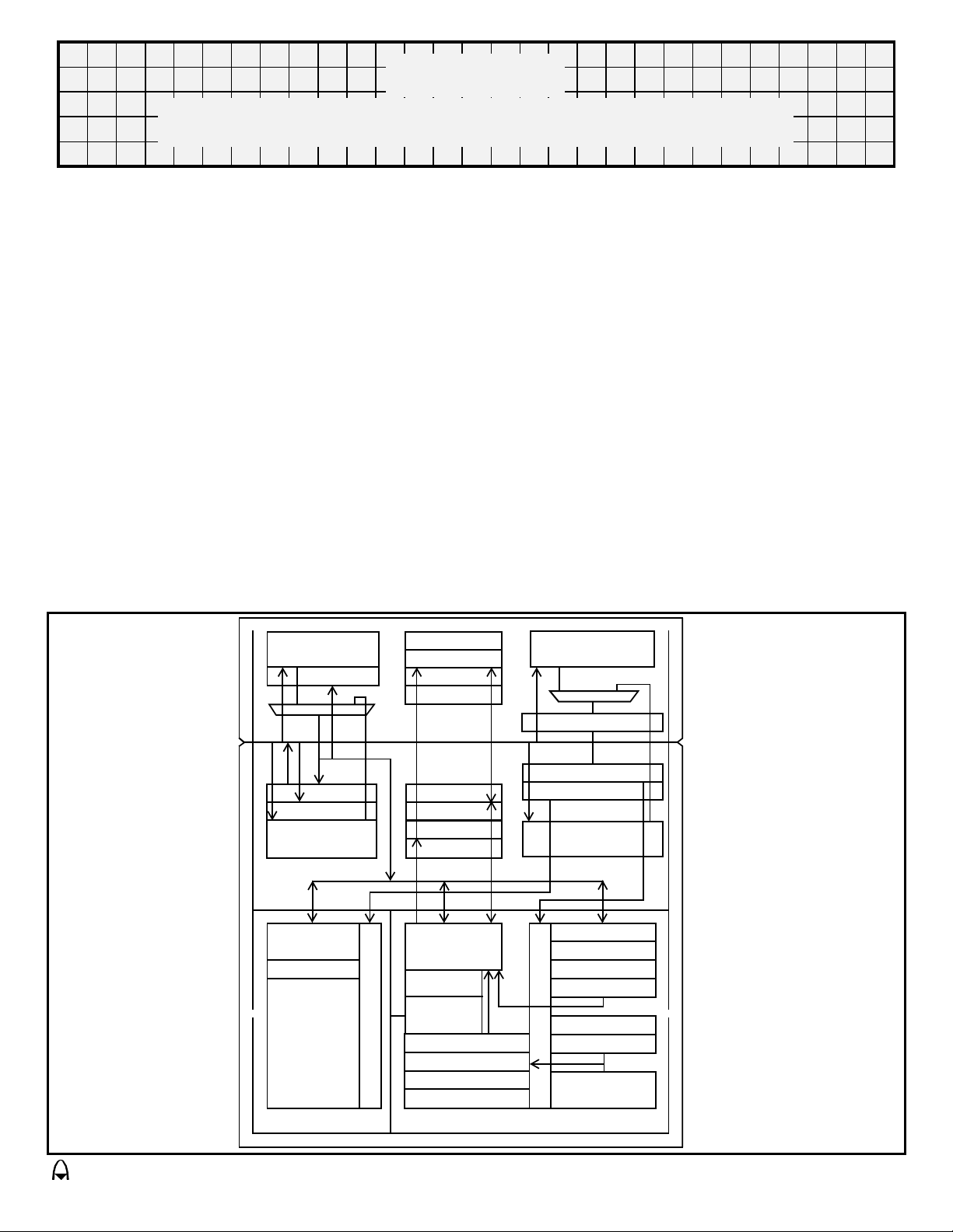
ACT ACT-5230PC-200F22T, ACT-5230PC-200F22M, ACT-5230PC-150F22C, ACT-5230PC Datasheet
ACT5230
32-Bit Superscaler Micropr ocessor
Features
■
Full militarized QED RM5230 microprocessor
■
Dual Issue superscalar microprocessor - can issue one
integer and one floating-point instruction per cycle
100, 133 and 150 MHz operating frequency – Consult
●
Factory for latest speeds
228 Dhrystone2.1 MIPS
●
SPECInt95 4.2 SPECfp95 4.5
●
■
System interface optomized for embedded
applications
32-bit system interface lower s total system cost wit h up to
●
87.5 MHz operating frequency
High performance write protocols maximize uncached
●
write bandwidth
Operates at processor clock divisors 2 through 8
●
5V tolerant I/O's
●
IEEE 1149.1 JTAG boundary scan
●
■
Integrated on-chip caches
16KB instruction - 2 way set associative
●
16KB data - 2 way set associative
●
Virtually indexed, physically tagged
●
Write-back and wri te-through on per page basis
●
Early restart on dat a cache misses
●
■
Integrated memory management unit
Fully associative joint TLB (shared by I and D translati ons)
●
48 dual entries map 96 pages
●
Va riable page size (4KB to 16MB in 4x increments)
●
■
High-performance floating point unit
Single cycle repeat rate for common si ngle precision
●
operations and some double precision operations
Two cycle repeat rate for double precision multiply and
●
double precision combined multiply-add operations
Single cycle repeat rate for single precision combined
●
multiply-add operation
■
MIPS IV instruction set
Floating point multiply-add instruction increases
●
performa nce in si gnal processing and graphics
applications
Conditional moves to reduce branch frequen cy
●
Index address modes (register + regist er)
●
■
Embedded application enhancements
Specialized DSP int eger Mu ltiply-Accumul ate instruction
●
and 3 operand multiply instruction
I and D cache lockin g by set
●
Optional dedicated exception vector for interrupts
●
■
Fully static CMOS design with power down logic
Standby reduced pow er mode with WAIT instruction
●
2.5 Wat ts typical with less than 70 mA standby current
●
■
128-pin Power Quad-4 package (F22),
Consult Fac tory for
package conf iguration
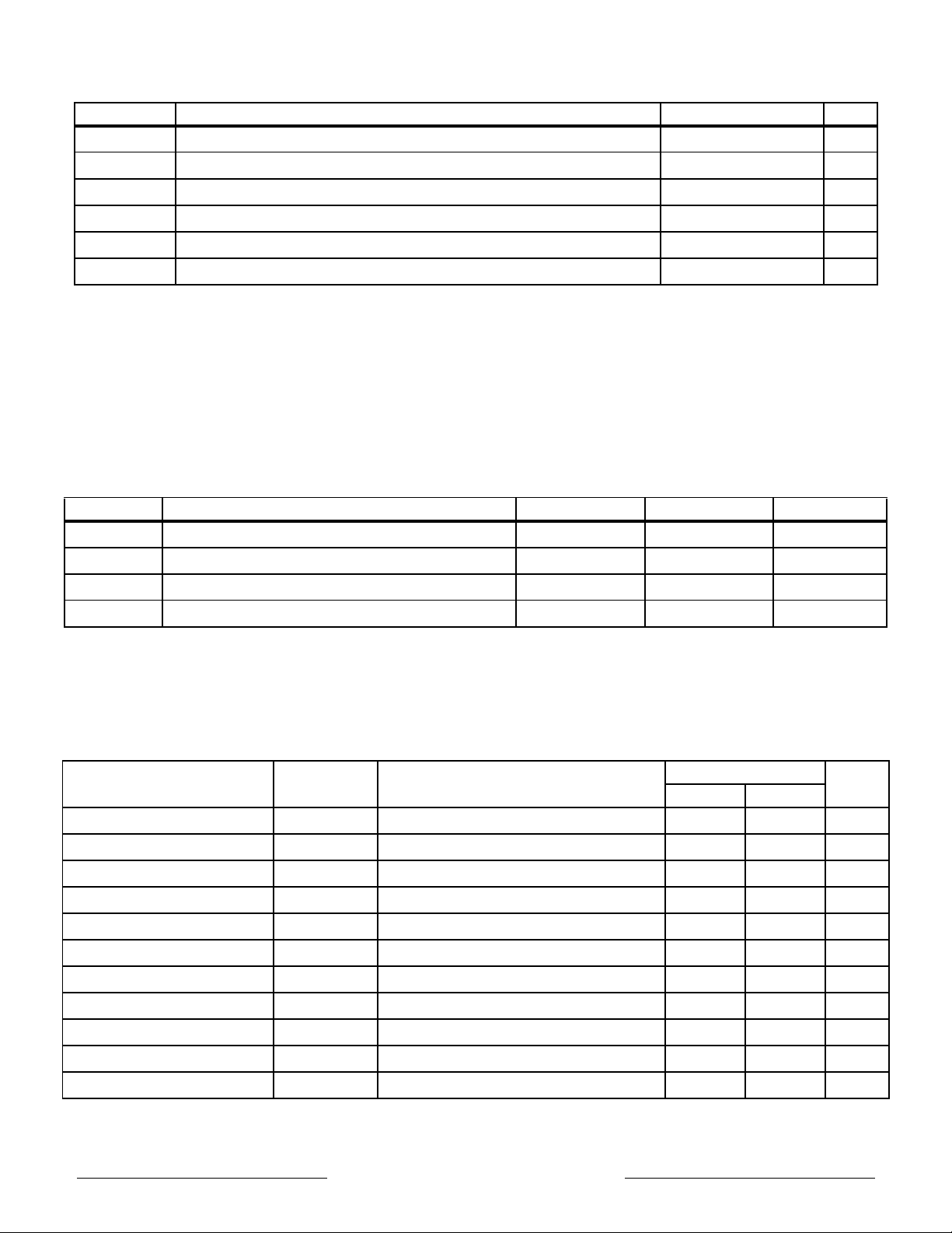
Block Diagram
Data Set A
Store B u ffer
Write Bu ffe r
Read Buffer
Data Set B
Control
Floating-point
Register File
Unpacker/Packer
Floati ng-point
MAdd, Add, Sub,Cvt
Div, SqRt
DBus
Sys AD
FPIBus
Floating point Control
Phase Lock Loop
Data Tag A
DTLB Physical
Data Tag B
Address Buffer
Instruction Tag A
ITLB Physical
Instruction Tag B
Tag Aux Tag
Joint TLB
Coprocessor 0
System/Memory
Control
PC Incrementer
Branch Adder
Instruction TLB Virtual
Program Counter
Instruction Set A
Instruction Select
Integer Instruction Register
FP Instruction Register
Instruction Set B
Integer/Address Adder
Integer Control
DVA
IVA
Integer Multiply, Divide
IntIBus
Load Aligner
Integer Register File
Data TLB Virtual
Sh ift e r/ S t o r e A l ig ner
Logic Unit
ABus
eroflex Circuit
Technology
Preliminary
– RISC TurboEngines For The Future © SCD5230 REV 1 12/22/98

DESCRIPTION
The ACT5230 is a highly integrated superscalar
microprocessor that implements a superset of the
MIPS IV Instruction Set Architecture(ISA). It has a
high performance 64-bit integer unit, a high
throughput, fully pipelined 64-bit floating point unit,
an opera ting system frie ndly memory ma nagement
unit with a 48-entry fully associative TLB, a 16 KByte
2-way set assoc iative ins tructio n cache , a 16 K Byte
2-way set associative data cache, and a
high-performance 32-bit system interface. The
ACT5230 can issue both an integer and a floating
point instruction in the same cycle.
The ACT5230 is ideally suited for high-end
embedded control applications such as
internetworking, high performance image
manipulation, high speed printing, and 3-D
visualization.
HARDWARE OVERVIEW
The ACT5230 offers a high-level of integration
targeted at high-performance embedded
applications. Some of the key elements of the
ACT523 0 are briefly des c ribed below.
Superscalar Dispatch
The ACT5230 has an efficient asymmetric
superscal ar disp atch u nit w hic h allo ws it to i ssu e an
integer instruction and a floating-point computation
instruction simultaneously. With respect to
superscalar issue, integer instructions include alu,
branch, load/store, and floating-point load/store,
while flo ating-poin t computat ion instruc tions inc lude
floating- point add, subtra ct, combined m ultiply-add,
converts, etc. In combination with its hig h throughput
fully pipelined floating-point execution unit, the
superscalar capability of the ACT5230 provides
unparalleled price/performance in computationally
intensive embedded applications.
CPU Registers
Like all M IPS ISA proce ssors, the A CT5230 CPU
has a simple, clean user visible state consisting of 32
general purpose registers, two special purpose
registers for integer multiplication and division, a
program c ounter, and no conditio n c ode bits.
therefore fully upward compatible with applications
that run on processors implementing the earlier
generation MIPS I-III instruction sets. Additionally,
the ACT5230 includes two implementation specific
instruct ions not foun d in the base line MIPS IV ISA
but that are useful in the embedded market place.
Describe d in detail in the QED RM5230 datasheet,,
these instructions are integer multiply-accumulate
and 3-operand integer multiply.
The ACT5230 integer unit includes thirty-two
general purpose 64-bit registers, a load/store
architecture with single cycle ALU operations (add,
sub, logical, shift) and an autonomous multiply/divide
unit. Additional register resources include: the HI/LO
result r egisters for the t wo-op erand in teger m ultiply/
divide operations, and the prog ram counte r(PC).
Register File
The ACT5230 has thirty-two general purpose
registe rs with registe r locat ion 0 h ard wired to zero.
These registers are used for scalar integer
operatio ns a nd addr ess cal cula tion. T he r eg ister f ile
has two read ports and one write port and is fully
bypassed to minimize operation latency in the
pipeline.
ALU
The ACT5230 ALU consists of the integer adder/
subtra ctor, the logic un it, and the shifter. The adder
performs address calculations in addition to
arithmetic operations, the logic unit performs all
logical and zero shift data moves, and the shifter
performs shifts and store alignment operations. Each
of these units is optimized to perform all operations in
a single processor cycle
For Detail Information regarding the operation of
the Quantum Effect Design (QED) RISCMark
RM5230, 32-Bit Superscalar Microprocessor see
the QED dat asheet (R ev is ion 1.2 July 1998).
Pipeline
For integer operations, loads, stores, and other
non-floating-point operations, the ACT5230 uses the
simple 5-stage pipeline also found in the QED
circuits R4600, R4700, and R5000. In addition to this
standard pipeline, the ACT5230 uses an extended
seven stage pipeline for floating-point operations.
Like the QED R5000, th e ACT5230 d oes virtual to
physical t ranslation in p arallel with ca c he access.
Integer Unit
Like the QED R5000, the ACT5230 implements
the MIPS IV Instruction Set Architecture, and is
Aeroflex Cir cuit Technology
2
SCD5230 REV 1 12/22/98 Plainview NY (516) 694-6700
Absolute Maximum Ratings
1
Symbol Rating Range Units
T
TERM
T
CASE
T
BIAS
T
STG
I
IN
I
OUT
Notes:
1. Stresses above those listed under "AbsoluteMaximums Rating" may cause permanent damage to the device. This is a stress rating only and functional operation
of the device at these or any other conditions above those indicated in the operational sections of this specification is not implied. Exposure to absolute maximum rating
conditions for extended periods may affect device reliability.
2. V
minimum = -2.0V for pulse width less than 15nS. VIN maximum should not exceed +5.5 Volts.
IN
3. When V
4. No more than one output should be shorted at one time. Duration of the short should not exceed more than 30 second.
IN
Terminal Voltage with respect to GND
Operating Temperature
Case Temperature under Bias
Storage Temperature
DC Input Current
DC Output Current
< 0V or VIN > Vcc.
2
-0.5
to 4.6 V
0 to +85 °C
-55 to +125 °C
-55 to +125 °C
3
20
mA
50 mA
Recommended Operating Conditions
Symbol Parameter Minimum Maximum Units
V
CC
V
IH
V
IL
T
C
Power Supply Voltage
Input High Voltage
Input Low Voltage
Operating Temperature Case (Commercial)
+3.135 +3.465 V
0.7V
CC
-0.5 0.2V
V
+ 0.5 V
CC
CC
0 +85 °C
V
DC Characteristics
(VCC = 3.3V ±5%; T
Parameter Sym Conditions
Output Low Voltage
Output High Voltage
Output Low Voltage
Output High Voltage
Input High Voltage
Input Low Voltage
Input Current
Input Current
Input Current
Input Capacitance
Output Capacitance
Aeroflex Cir cuit Technology
V
V
V
V
C
OL1
OH1
OL2
OH2
V
V
I
IN1
I
IN2
I
IN3
C
OUT
IOL = 20 µA
IOL = 20 µA
IOL = 4 mA
IOL = 4 mA
IH
IL
V
= 0V
IN
V
= V
IN
CC
V
= 5.5V
IN
IN
CASE
= 0°C to +85°C)
3
133 / 150MHz
Min
Max
Units
0.1 V
Vcc - 0.1 V
0.4 V
2.4 V
0.7V
-0.5 0.2V
CC
V
+ 0.5 V
CC
CC
V
-20 +20 µA
-20 +20 µA
-250 +250 µA
10 pF
10 pF
SCD5230 REV 1 12/22/98 Plainview NY (516) 694-6700
 Loading...