

ACT ACT4489-I, ACT4489-FI, ACT4489-F, ACT4489 Datasheet
www.aeroflex.com/act1.htm
ACT 4489 SINGLE TRANSCEIVER
FOR MIL-STD-1553/1760
Features
• +5 / ±12 Volt Supply Operation
• Low Power Dissipation
• Small Size & Light Weight
• Outstanding MIL-STD-1553 performance
• Radiation Hard Dielectric Isolation Monolithic
Construction for Severe Environments
• Superior High Frequency Line Transient and
Input Ripple Rejection
• Input and Output TTL Compatible Design
• Processed and Screened to MIL-STD-883 Specs
• MIL-PRF-38534 Compliant Devices Available
CIRCUIT TECHNOLOGY
General Description
The Aeroflex Circuit
Technology ACT 4489 is a next
generation monolithic transceiver
design which provides full
compliance to MIL-STD-1553A/B
and 1760 requirements in a small
package with low power
consumption.
The ACT4489 series performs
the front-end analog function of
inputting and outputting data
through a transformer to the
MIL-STD-1553 data bus.
Design of this transceiver reflects
particular attention to active filter
performance. This results in low bit
and word error rate with superior
waveform purity and minimal zero
crossover distortion. Efficient
transmitter electrical and thermal
design provides low internal power
dissipation and heat rise at high as
well as low duty cycles.
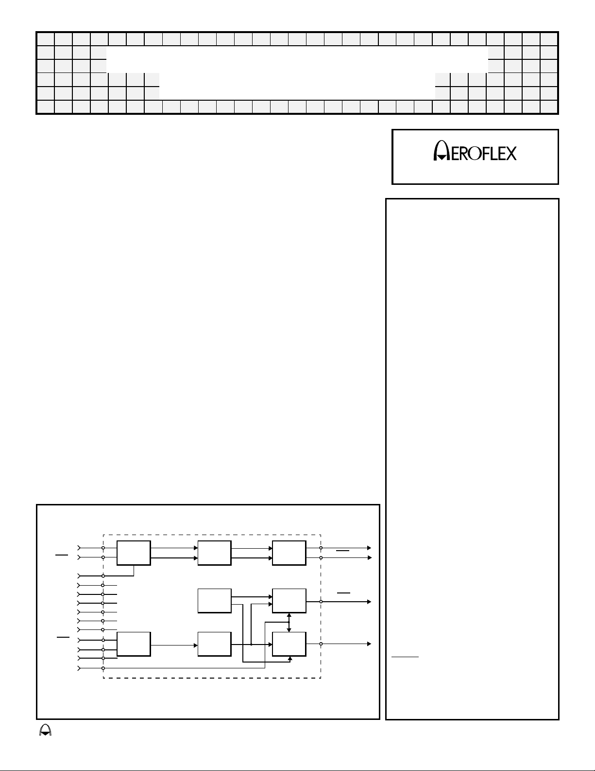
Transmitter:
TX DATA IN
TX DATA
TX INHIBIT IN
+5V (VL)
+12V (VCC)
-12V (VEE)
GND1
GND2
GND3
RX DATA
RX DATA IN
CASE
RX STROBE IN
IN
IN
DRIVER
INPUT
AMPLIFIER
ACTIVE
FILTER
REFERENCE
ACTIVE
FILTER
OUTPUT
STAGE
COMP.
COMP.
TX DATA OUT
TX DATA
OUT
OUT
RX DATA
RX DATA OUT
Block Diagram (Without Transformer)
The Transmitter section accepts
bi-phase TTL data at the input and
when coupled to the data bus with a
1:1 ratio transformer, isolated on
the data bus side with two 52.5
Ohm fault isolation resistors, and
loaded by two 70 Ohm
terminations, the data bus signal is
typically 7 Volts P-P at point A (See
Figure5). When both DATA and
DATA
inputs are held low or high,
the transmitter output becomes a
high impedance and is “removed”
from the line. In addition, an
overriding “INHIBIT" input provides
eroflex Circuit Technology – Data Bus Modules For The Future © SCD4489 REV A 1/29/98
for the removal of the transmitter
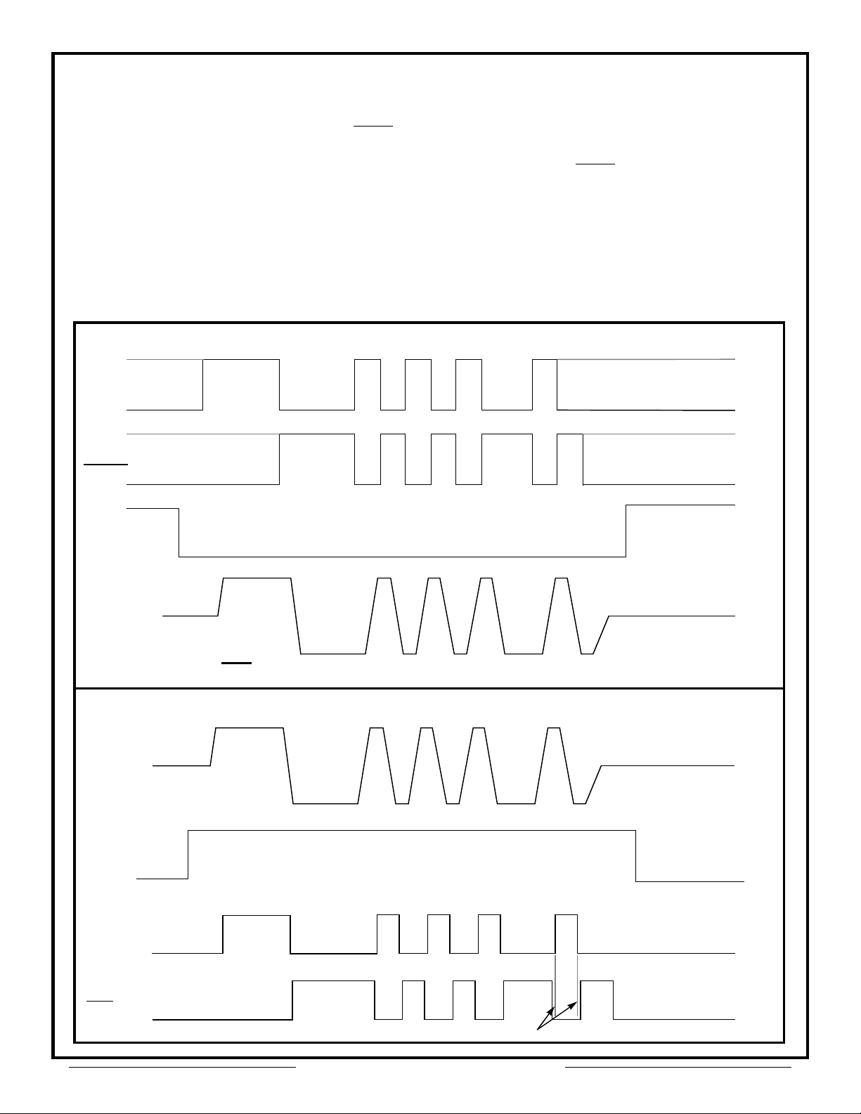
Note overlap
output from the line. A logic “1”
signal applied to the “INHIBIT” takes
priority over the condition of the
data inputs and disables the
transmitter (See Transmitter Logic
Waveform, Figure1). The
Transmitter may be safely operated
for an indefinite period with the bus
(point A) short circuited at 100%
duty cycle.
Receiver:
The Receiver section accepts
bi-phase differential data at the
input and produces two TTL signals
at the output. The outputs are DATA
and DATA
, and represent positive
and negative excursions of the input
beyond a pre-determined threshold
(See Receiver Logic Waveform,
Figure 2).
The pre-set internal thresholds will
detect data bus signals, point A
Figure 5, exceeding 1.20 Volts P-P
and reject signals less than 0.6
Volts P-P when used with a
Figure 1 — Transmitter Logic Waveforms Idealized
DATA IN
DATA IN
transformer (See Figure 5 for
transformer data and typical
connection).
A low level at the RX Strobe
input inhibits the DATA and
DATA
outputs. If unused, a 2K
pull-up to +5 Volts is
recommended.
INHIBIT
LINE TO LINE
OUTPUT
Note:
DATA and DATA
and must be in the same state during off times (both high or low).
inputs must be complementary waveforms or 50% duty cycle average, with no delays between them,
Figure 2 — Receiver Logic Waveforms Idealized (ACT4489)
LINE TO LINE
INPUT
STROBE
DATA OUT
DATA OUT
Aeroflex Circuit Technology SCD4489 Rev A 1/29/98 Plainview NY (516) 694-6700
2
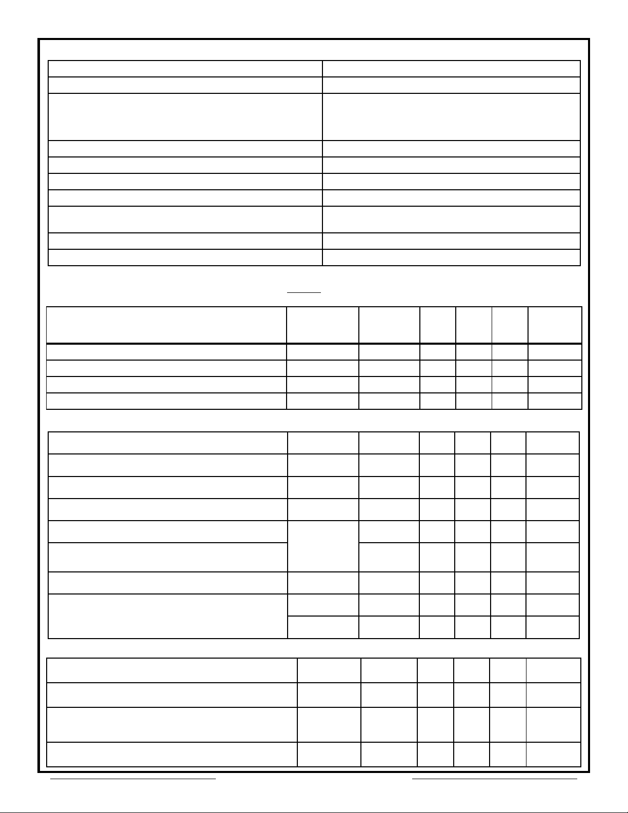
Absolute Maximum Ratings
Operating case temperature -55°C to +125°C
Storage case temperature -65°C to +150°C
Power supply voltage
CC
V
VEE
VL
-0.3 V to +18 V
+0.3 V to-18 V
-0.3 V to +7.0 V
Logic input voltage -0.3 V to +5.5 V
Receiver differential input ±40 V
Receiver input voltage (common mode) ±10 V
Driver peak output current 300 mA
Total package power dissipation over the full operating
2.5 Watts
case temperature rise
Maximum junction to case temperature 10°C
Thermal resistance – junction to case 4°C/W
Electrical Characteristics — Driver Section
Input Characteristics, TX DATA IN or TX DATA IN (Notes 2 & 3 apply)
P-P
Parameter Condition Symbol Min Typ
"0" Input Current VIN = 0.4 V I
"1" Input Current V
= 2.7 V I
IN
"0" Input Voltage V
"1" Input Voltage V
ILD
IHD
IHD
IHD
2.0 V
-0.1 -0.2
Inhibit Characteristics
"0" Input Current
"1" Input Current
"0" Input Voltage
"1" Input Voltage
Delay from TX inhibit, (0→1) to inhibited output From mid pt
Delay from TX inhibit, (1→0) to active output
Differential output noise, inhibit mode
Differential output impedance (inhibited) Note 1
See Figure 5
= 0.4 V I
V
IN
=2.7V I
V
IN
inhibit to
±1.2V pt B,
See Figure 5
Point B
Point C
ILI
IHI
V
ILI
V
IHI
t
DXOFF
t
DXON
V
NOI
Z
OI
Z
OI
-0.1 -0.2
1.0 40
2.0
175 225
90 150
2K
1K
Ma
x
Unit
mA
1 40 µA
0.7
mA
µA
0.7
V
V
nS
nS
2 10 mV
Ω
Ω
V
P-P
Output Characteristics
Differential output level,
See Figure 5
Rise and fall times(10% to 90% at pt A output)
See Figure 5
Output offset, Figure 3, 2.5µS after midpoint
crossing of the parity bit of the last word of a 660µS
Point A V
Point A
Point A
V
t
OS
O
r
6 7 9
100 160 300 nS
± 90
message See Figure 5
Delay from 50% point of TX DATA or TX DATA
to zero crossing of differential signal. See Fig 5
Aeroflex Circuit Technology SCD4489 Rev A 1/29/98 Plainview NY (516) 694-6700
input
Point A t
3
DXT
100 200
V
mV peak
nS
P-P
 Loading...