

ACT ACT4468DI, ACT4468DFI, ACT4468DF, ACT4468D Datasheet
eroflex Circuit T
– Data Bus Modules For The Future © SCD4468D REV B 5/25/00
Features
ACT4468D Dual Transceiver
ACT4468D
Dual Transceivers for MIL-STD-1553
• World’s smallest and lowest standby power dual
transceiver 0.3" x 1" packages
• Dual transceiver meets military data bus
requirements, MIL-STD-1553 and MIL-STD-1760
• Low power dissipation at full output power
• Single +5V power supply
• Current source output
• Monolithic construction using dielectrically
isolated(D.I.)
• Processed and screened to MIL-STD-883 specs
• DESC SMD# 5962–92061 Pending
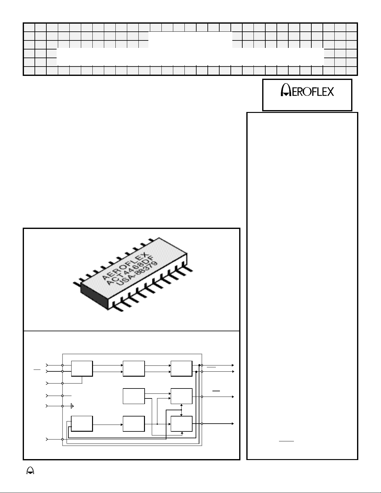
TX DATA IN
TX DATA IN
TX INHIBIT
+5 V
GROUND
STROBE
DRIVER
INPUT
AMP
SHAPING
REFERENCE
ACTIVE
FILTER
OUTPUT
STAGE
COMP.
COMP.
Block Diagram (without Transformer), 1/2 of unit shown
TX/RX
TX/RX
RX DATA OUT
RX DATA OUT
CIRCUIT TECHNOLOGY
www.aeroflex.com
General Description
The Aeroflex Circuit Technology
Model ACT4468D is a next
generation D.I. monolithic transceiver
which provide full compliance with
MIL-STD-1553/1760 and data bus
requirements in the smallest
packages with the lowest standby
power consumption and one power
supply operation.
The dual channel Model ACT4468D
perform the front-end analog function
of inputting and outputting data
through a transformer to a
MIL-STD-1553/1760 data bus.
Design of these transceivers reflects
particular attention to active filter
performance. This results in low bit
and word error rate with superior
waveform purity and minimal zero
crossover distortion. Efficient
transmitter electrical and thermal
design provides low internal power
dissipation and heat rise at high as
well as low duty cycles.
Each channel of the dual transceiver
is completely separate from the other
and fully independent. This includes
power leads as well as signal lines.
Hence, each channel may be
connected to a different data bus with
no interaction.
Transmitter:
The Transmitter section accepts
bi-phase TTL data at the input and
when coupled to the data bus with a
1:2.5 transformer, isolated on the
data bus side with two 52.5 Ohm fault
isolation resistors, and loaded by two
70 Ohm terminations plus additional
receivers, the data bus signal
produced is 7.5Volts nominal P-P at
A-A’. (See Figure 5.) When both
DATA and DATA
high, the transmitter output becomes
inputs are held low or
echnology
Aeroflex Circuit Technology
SCD4468D REV B 5/25/00 Plainview NY (516) 694-6700
CIRCUIT TECHNOLOGY
a high impedance and is “removed”
from the line. In addition, an
overriding “INHIBIT" input provides
for the removal of the transmitter
output from the line. A logic “1”
applied to the “INHIBIT” takes
priority over the condition of the data
inputs and disables the transmitter.
(See Transmitter Logic Waveform,
Figure 1.)
The transceiver utilizes an active
filter to suppress harmonics above
1MHz. The Transmitter may be
safely operated at 100% duty cycle
for an indefinite period into a short
circuited 1553 bus.
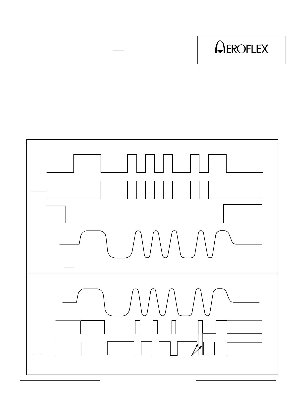
Figure 1. Transmitter Logic Waveforms
DATA IN
Receiver:
The Receiver section accepts
bi-phase differential data at the input
and produces two TTL signals at the
output. The outputs are DATA and
, and represent positive and
DATA
negative excursions of the input
beyond a pre-determined
threshold.(See Receiver Logic
Waveform. Figure 2.)
The pre-set internal thresholds will
detect data bus signals exceeding
1.150 Volts P-P and reject signals
less than 0.6 volts P-P when used
with a 1:2.5 turns ratio transformer.
(See Figure 5 for transformer data
and typical connection.)
DATA IN
INHIBIT
LINE TO LINE
OUTPUT
NOTES:
1.DATA and DATA
2.DATA and DATA
inputs must be complementary waveforms or 50% duty cycle average, with no delays between them.
must be in the same state during off time (both high or low).
Figure 2. Receiver Logic Waveforms
LINE TO LINE
INPUT
DATA OUT
DATA
OUT
NOTE: Waveforms shown are for normally low devices. For normally high receiver output
Note overlap
level devices, the receiver outputs are swapped as shown by the dashed lines.
2
 Loading...