Page 1

0
S76S
LoRa Wireless Communication Module
H
901-10201
Mar 22
nd
, 2017
Product Name
Version
Doc No
Date
Page 2

S76S
LoRa Wireless Communication Module
H
901-10201
Mar 22th ,2017
1 of 18
Product Name
Version
Doc No
Date
Page
Date
Revised Contents
Revised By
Version
July 20th ,2016
Aug 25th ,2016
Sep 10th ,2016
Sep 26th ,2016
Oct. 7
th
,2016
Oct. 11
th
,2016
Mar 22nd ,2017
Nov 13nd ,2017
Draft Version
Revised 7.1 marking without logo
Revised marking with Acsip logo
Revised 4.1 footprint drawing
Update footprint
Add pin assignment, revise footprint and
mechanical dimension
Modify Marking information
Add FCC statement
Chunyi
Nick
Nick
Nick
Nick
Kenny
Kenny
Kenny
A
B
C
D
E
F
G
H
Document History
Page 3

S76S
LoRa Wireless Communication Module
H
901-10201
Mar 22th ,2017
2 of 18
Product Name
Version
Doc No
Date
Page
1. General Description
The S76S integrates ARM Coretex®-M0+ (32-bit RISC core operating at a 32MHz frequency) MCU with LoRaTM
modulation that provides ultra-long range spread spectrum communication and high interference immunity
whilst minimizing current consumption.
S76S can achieve a sensitivity of over -137 dBm. The high sensitivity combined with the integrated +20 dBm
power amplifier yields industry leading link budget making it optimal for any low data rate application requiring
range or robustness. LoRaTM also provides significant advantages in both blocking and selectivity over
conventional modulation techniques, solving the traditional design compromise between range, interference
immunity and energy consumption.
Feature
Small footprint:13 mm x 11 mm x 1.1 mm
LoRa
+20 dBm constant RF output vs. V supply
Programmable bit rate up to 37500 bps
High sensitivity: down to -137 dBm
Excellent blocking immunity
TM
Modem
Preamble detection
Automatic RF Sense and CAD with ultra-fast AFC
Payload up to 128 bytes with CRC
Embedded memories (up to 192 Kbytes of
Flash memory and 20 Kbytes of RAM)
Page 4

S76S
LoRa Wireless Communication Module
H
901-10201
Mar 22th ,2017
3 of 18
Product Name
Version
Doc No
Date
Page
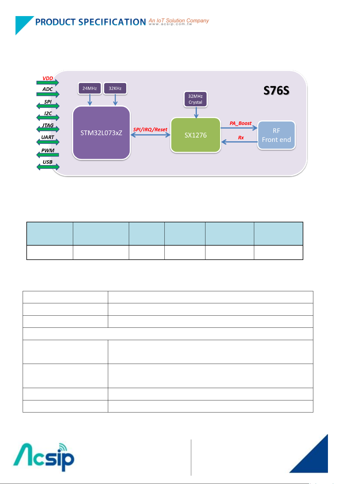
1-1 Block Diagram
Part
Number
Frequency
Range
Spreading
Factor
Bandwidth
(K Hz)
Effective
Bitrate (bps)
Est. Sensitivity
( dBm )
S76S
902.3-914.9 MHz
6 - 12
62.5 - 500
146 - 37500
-109 to -137*
Model Name
S76S
Product Description
LoRa Wireless Communication Module
Host Interface
UART
Operation Conditions
Temperature
Storage:-50℃ ~ +105℃
Operating:-20℃ ~ +70℃
Humidity
Operating:10 ~ 95% (Non-Condensing)
Storage:5 ~ 95% (Non-Condensing)
Dimension
13 mm x 11 mm x 1.1 mm
Package
LGA type
A simplified block diagram of the S76S module is depicted in the figure below.
1-2 Product Version
The features of S76S is detailed in the following table
Note: * LORA setting SF=12, BW=62.5k, Long-Range Mode, highest LNA gain, LnaBoost for Band 1.
1-3 Specification
Page 5

S76S
LoRa Wireless Communication Module
H
901-10201
Mar 22th ,2017
4 of 18
Product Name
Version
Doc No
Date
Page
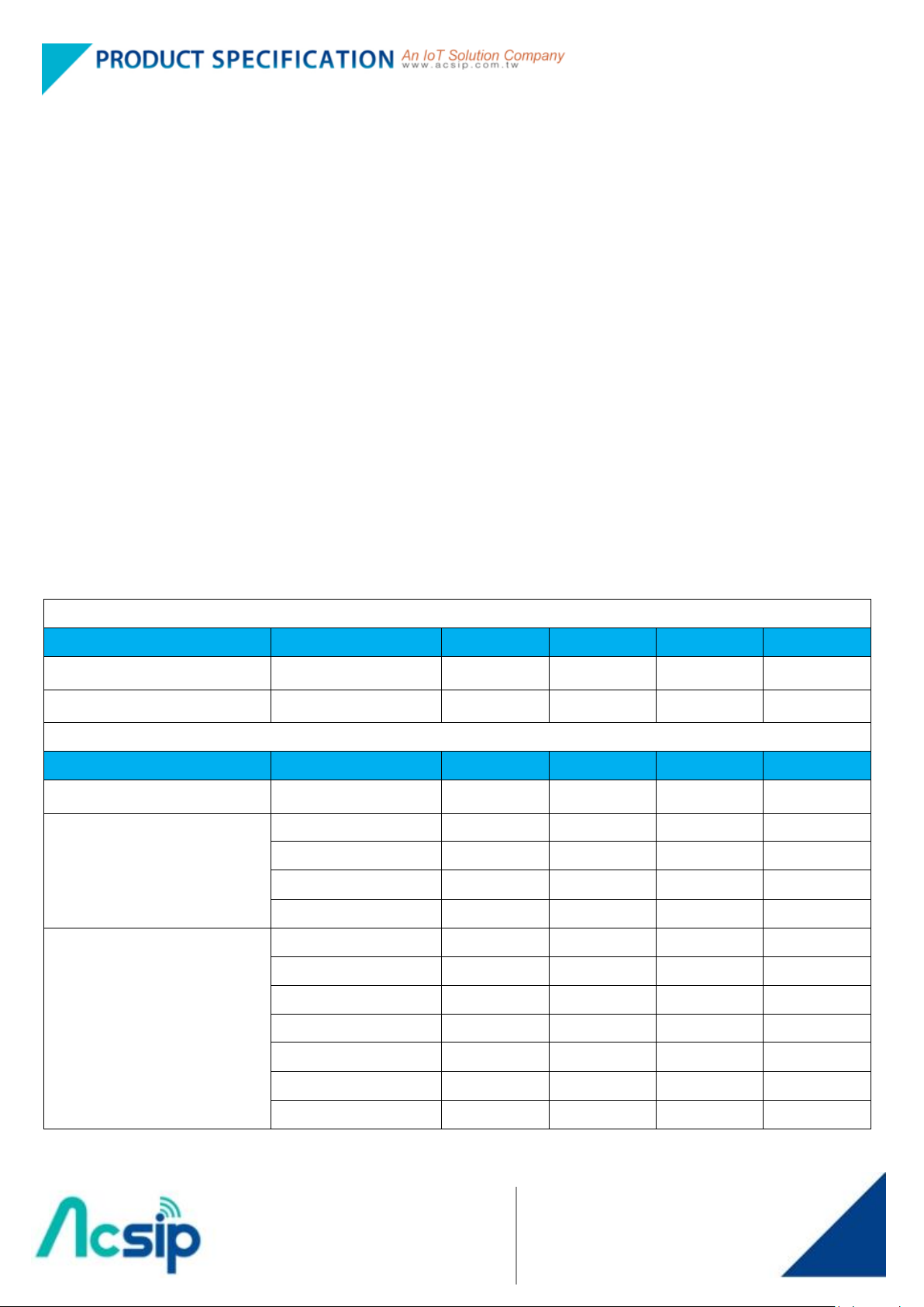
2. Electrical Characteristics
Symbol
Parameter
Min.
Typ.
Max.
Unit
VDD33
Supply Voltage
-0.3
3.9 V VIN
Input voltage on digital pins
-0.3
3.9 V Pmr
RF Input Level
+10
dBm
Symbol
Parameter
Min.
Typ.
Max.
Unit
VDD33
Supply Voltage
2.0
3.3
3.6
V
ML
RF Input Level
+10
dBm
Symbol
Parameter
Conditions
Typ.
Max.
Unit
IDDSL
Supply current in Sleep mode
TBD
uA
IDDST
Supply current in Standby mode
Crystal oscillator enabled
9
9.6
mA
IDDR
Supply current in Receive mode
17.5
mA
IDDT
Supply current in Transmit
mode with impedance
matching
RFOP = +20 dBm
RFOP = +17 dBm
RFOP = +13 dBm
RFOP = + 7 dBm
127
82
65
49
mA
2-1. Absolute Maximum Ratings
2-2. Recommended Operating Range
2-3. Power Consumption Characteristics
Page 6

S76S
LoRa Wireless Communication Module
H
901-10201
Mar 22th ,2017
5 of 18
Product Name
Version
Doc No
Date
Page
LoRa Transmitter (Conductive)
Item
Condition
Min.
Typ.
Max.
Unit
Frequency Range
Band1
915
MHz
Tx Power Level
PA_BOOST pin
18.0
19.5
21.0
dBm
LoRa Receiver (Conductive)
Item
Condition
Min.
Typ.
Max.
Unit
Frequency Range
Band1
863
915
928
MHz
RFS_L62_HF
(Long-Range Mode, highest
LNA gain, LNA boost, 62.5
kHz bandwidth)
SF = 6
-119
dBm
SF = 7
-114
dBm
SF = 8
-127
dBm
SF = 12
-137
dBm
RFS_L500_HF
(Long-Range Mode, highest
LNA gain, LNA boost, 500
kHz bandwidth)
SF = 6
-109
dBm
SF = 7
-114
dBm
SF = 8
-117
dBm
SF = 9
-120
dBm
SF = 10
-123
dBm
SF = 11
-126
dBm
SF = 12
-128
dBm
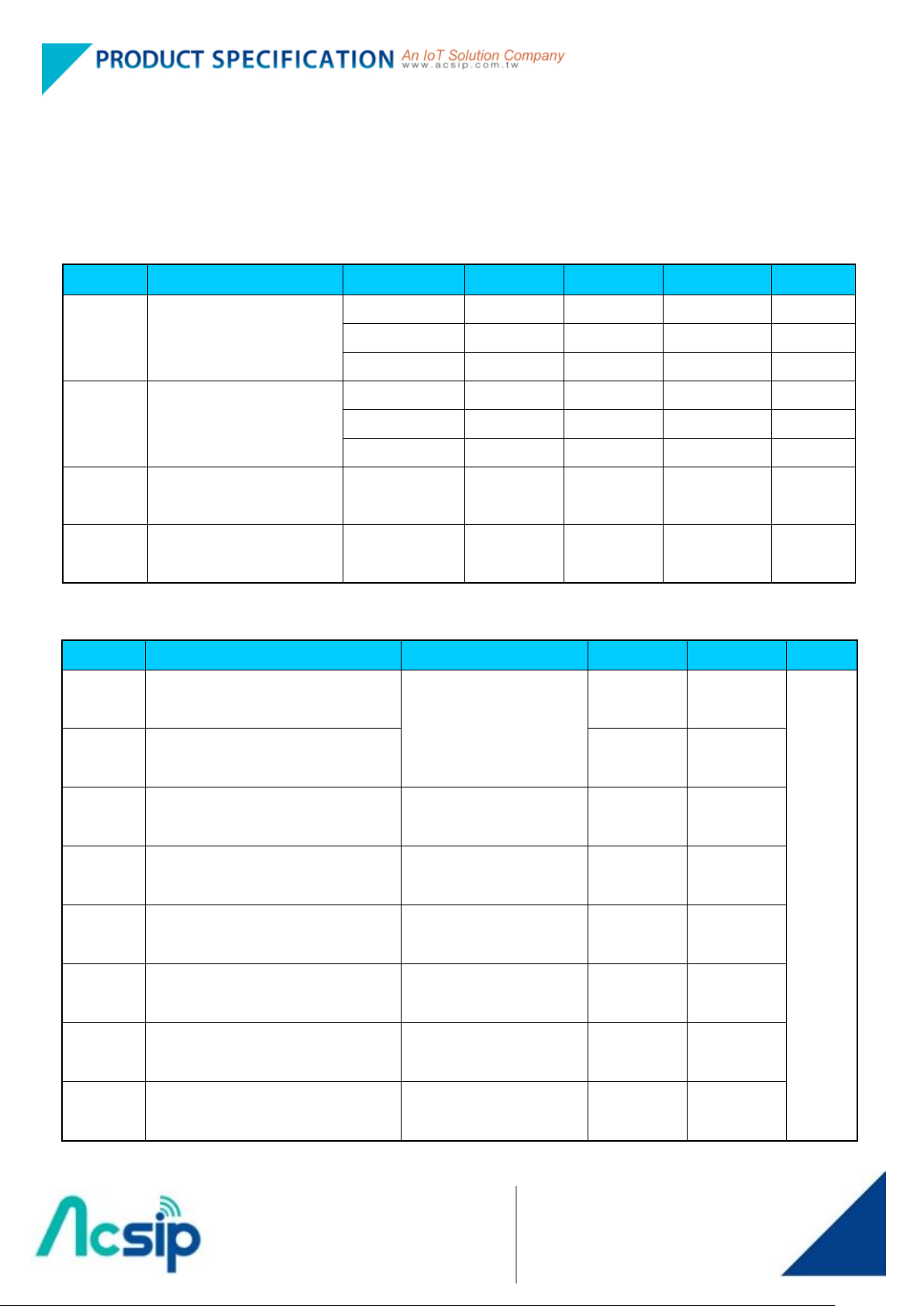
2-4. RF Characteristics
The table below gives the electrical specifications for the transceiver operating with LoRaTM modulation.
Following conditions apply unless otherwise specified:
Supply voltage = 3.3 V.
Te mperature = 25° C.
Frequency bands: 915 MHz
Bandwidth (BW) = 125 kHz.
Spreading Factor (SF) = 12.
Error Correction Code (EC) = 4/6.
Packet Error Rate (PER)= 1%
CRC on payload enabled.
Output power = 13 dBm in transmission.
Payload length = 64 bytes.
Preamble Length = 12 symbols (programmed register PreambleLength=8)
With matched impedances
Page 7

S76S
LoRa Wireless Communication Module
H
901-10201
Mar 22th ,2017
6 of 18
Product Name
Version
Doc No
Date
Page
2-5. Digital Characteristics
Symbol
Description
Conditions
Min
Typ.
Max
Unit
VIH
I/O input
high level voltage
NRST
0.7xVDD33
- - V
BOOT0
0.7xVDD33
- - V
GPIO
0.7xVDD33
- - V
VIL
I/O input
low level voltage
NRST
- - 0.3xVDD33
V
BOOT0
- - 0.14xVDD33
V
GPIO
- - 0.3xVDD33
V
RPU
Weak pull-up
Equivalent resistor
VIN = GND
30
45
60
K Ω
RPD
Weak pull-down
Equivalent resistor
VIN =VDD33
30
45
60
K Ω
Symbol
Description
Conditions
Min
Max
Unit
VOL
Output low level voltage for
an I/O pin
CMOS port / IIO = +8
mA
2.7 V≦VDD33≦3.6 V
-
0.4 V VOH
Output high level voltage for
an I/O pin
VDD33-0.4
-
VOL
Output low level voltage for
an I/O pin
TTL port / IIO =+ 8 mA
2.7 V≦VDD33≦3.6 V
-
0.4
VOH
Output high level voltage for
an I/O pin
TTL port / IIO =- 6 mA
2.7 V≦VDD33≦3.6 V
2.4
-
VOL
Output low level voltage for
an I/O pin
IIO = +15 mA
2.7 V≦VDD33≦3.6 V
-
1.3
VOH
Output high level voltage for
an I/O pin
IIO = -15 mA
2.7 V≦VDD33≦3.6 V
VDD33-1.3
-
VOL
Output low level voltage for
an I/O pin
IIO = +4 mA
1.65 V≦VDD33≦3.6 V
-
0.45
VOH
Output high level voltage for
an I/O pin
IIO = +4 mA
1.65 V≦VDD33≦3.6 V
VDD33-0.45
-
2-5-1. DC characteristics
Input voltage levels
Output voltage levels
Page 8

S76S
LoRa Wireless Communication Module
H
901-10201
Mar 22th ,2017
7 of 18
Product Name
Version
Doc No
Date
Page
Symbol
Description
Conditions
Min
Typ.
Max
Unit
V
IL(NRST)
NRST input low level
voltage
VSS 0.8
V
V
IH(NRST)
NRST input high level
voltage
1.4
VDD33
V
V
OL(NRST)
NRST output low level
voltage
IOL = 2mA
2.7V<VDD33<3.6V
0.4
V
V
OL(NRST)
NRST output low level
voltage
IOL = 1.5mA
1.65V<VDD33<2.7V
0.4
V
V
hys(NRST)
NRST schmitt trigger
voltage hysteresis
10%
VDD33
mV
R
PU
Weak pull-up
Equivalent resistor
VIN = GND
30
45
60
K Ω
VF
NRST Input filtered pulse
50
nS
VNF
NRST Input not filtered
pulse
VDD33 > 2.7 V
350
nS
2-5-2. NRST pin characteristics
The NRST pin input driver uses CMOS technology.
It is connected to a permanent pull-up resistor (RPU).
The following figure is recommended NRST pin protection circuit against parasitic resets.
Page 9

S76S
LoRa Wireless Communication Module
H
901-10201
Mar 22th ,2017
8 of 18
Product Name
Version
Doc No
Date
Page
2-5-3. UART Interface Parameters
Baud Rate = 38400 bps
Data Bits = 8 bits
Stop Bits = 1 bit
Parity Check = None
Flow Control = None
Page 10

S76S
LoRa Wireless Communication Module
H
901-10201
Mar 22th ,2017
9 of 18
Product Name
Version
Doc No
Date
Page
Pin
Definition
I/O
Description
1
NC
2
GND
Ground pin
3
GND
Ground pin
4
PC0
I/O
MCU pin name: PC0
5
PC1
I/O
MCU pin name: PC1
6
PC2
I/O
MCU pin name: PC2
7
PC3
I/O
MCU pin name: PC3
8
NC
9
NC
10
NC
11
NC
12
NRST
Hardware reset pin
13
PA0
I/O
MCU pin name: PA0
14
GND
Ground pin
15
GND
Ground pin
16
PA2_TXD_A
I/O
MCU pin name: PA2
17
PA3_RXD_A
I/O
MCU pin name: PA3
18
PA4_SPI1_NSS
I/O
MCU pin name: PA4
19
PA5_SPI1_SCK
I/O
MCU pin name: PA5
20
PA6_SPI1_MISO
I/O
MCU pin name: PA6
21
PA7_SPI1_MOSI
I/O
MCU pin name: PA7
22
PC4
I/O
MCU pin name: PC4
23
PC5
I/O
MCU pin name: PC5
24
PB0_IO_INT1
I/O
MCU pin name: PB0
25
PB1_IO_INT2
I/O
MCU pin name: PB1
26
PC6
I/O
MCU pin name: PC6
27
PC7
I/O
MCU pin name: PC7
28
PC8
I/O
MCU pin name: PC8
29
PC9
I/O
MCU pin name: PC9
30
RXTX/RFMOD
O
Control signal from SX1276, which connects to internal RF switch at
the same time.
3. Pin Definition
Page 11

S76S
LoRa Wireless Communication Module
H
901-10201
Mar 22th ,2017
10 of 18
Product Name
Version
Doc No
Date
Page
31
GND
Ground pin
32
GND
Ground pin
33
RF_ANT
I/O
RF I/O
34
GND
Ground pin
35
GND
Ground pin
36
PA1_RF_FEM_CPS
I/O
MCU pin name: PA1
37
GND
Ground pin
38
NC
39
GND
Ground pin
40
NC
41
GND
Ground pin
42
NC
43
VDD33
Power Supply
44
VDD33
Power Supply
45
PA8_USART1_CK
I/O
MCU pin name: PA8
46
PA10_USART1_RX
I/O
MCU pin name: PA10
47
PA9_USART1_TX
I/O
MCU pin name: PA9
48
PA11_USART1_CTS
I/O
MCU pin name: PA11
49
PA12_USART1_RTS
I/O
MCU pin name: PA12
50
PA13_SWDIO
Serial wire (SWD) debug interface
51
PA14_SWCLK
Serial wire (SWD) debug interface
52
PC10
I/O
MCU pin name: PC10
53
PC11
I/O
MCU pin name: PC11
54
PC12
I/O
MCU pin name: PC12
55
PD2
I/O
MCU pin name: PD2
56
PB5
I/O
MCU pin name: PB5
57
PB6_SCL
I/O
MCU pin name: PB6
58
PB7_SDA
I/O
MCU pin name: PB7
59
BOOT0
I
Boot mode selection pin
60
PB8_IO_LED_FCT
I/O
MCU pin name: PB8
61
GND
Ground Pin
62
GND
Ground Pin
Page 12

S76S
LoRa Wireless Communication Module
H
901-10201
Mar 22th ,2017
11 of 18
Product Name
Version
Doc No
Date
Page
3-1. Pin Assignment
The SiP module will conform to the following pin map, shown in the following diagram (top view)
Page 13

S76S
LoRa Wireless Communication Module
H
901-10201
Mar 22th ,2017
12 of 18
Product Name
Version
Doc No
Date
Page
4. Mechanical Dimension
Unit: mm
Page 14

S76S
LoRa Wireless Communication Module
H
901-10201
Mar 22th ,2017
13 of 18
Product Name
Version
Doc No
Date
Page
4-1 Recommended Footprint
Unit: mm
TOP View
Page 15

S76S
LoRa Wireless Communication Module
H
901-10201
Mar 22th ,2017
14 of 18
Product Name
Version
Doc No
Date
Page
5. Recommended Reflow Profile
Page 16

S76S
LoRa Wireless Communication Module
H
901-10201
Mar 22th ,2017
15 of 18
Product Name
Version
Doc No
Date
Page
6. SiP Module Preparation
6-1. Handling
Handling the module must wear the anti-static wrist strap to avoid ESD damage. After each module is
aligned and tested, it should be transport and storage with anti -static tray and packing. This protective
package must be remained in suitable environment until the module is assembled and soldered onto the
main board.
6-2. SMT Preparation
1. Calculated shelf life in sealed bag: 6 months at<40℃ and <90% relative humidity (RH).
2. Peak package body temperature: 250℃.
3. After bag was opened, devices that will be subjected to reflow solder or other high temperature
process must.
A. Mounted within: 168 hours of factory conditions<30℃/60%RH.
B. Stored at≦10%RH with N2 flow box.
4. Devices require baking, before mounting, if:
A. Package bag does not keep in vacuumed while first time open.
B. Humidity Indicator Card is >10% when read at 23±5℃.
C. Expose at 3A condition over 8 hours or Expose at 3B condition over 24 hours.
5. If baking is required, devices may be baked for 12 hours at 125±5℃.
Page 17

S76S
LoRa Wireless Communication Module
H
901-10201
Mar 22th ,2017
16 of 18
Product Name
Version
Doc No
Date
Page
Pin 1 identifier
Production date code
Year/Week
Product part number
Lot Code
Acsip Logo
7. Package Information
7-1. Product Making
Figure 1 below details the standard product marking for all AcSiP Corp. products. Cross reference to the
applicable line number and table for a full detail of all the variables.
Figure 1 Standard Product Marking Diagram- TOP VIEW
Page 18

S76S
LoRa Wireless Communication Module
H
901-10201
Mar 22th ,2017
17 of 18
Product Name
Version
Doc No
Date
Page
7-2. Tray Dimension
Page 19

S76S
LoRa Wireless Communication Module
H
901-10201
Mar 22th ,2017
18 of 18
Product Name
Version
Doc No
Date
Page
7-3. Packing Information
7-4. Humidity Indicator Card
Page 20

S76S
LoRa Wireless Communication Module
H
901-10201
Mar 22th ,2017
19 of 18
Product Name
Version
Doc No
Date
Page
8. FCC statement
Federal Communication Commission Interference Statement
This equipment has been tested and found to comply with the limits for a Class B digital device,
pursuant to Part 15 of the FCC Rules. These limits are designed to provide reasonable protection
against harmful interference in a residential installation. This equipment generates, uses and can
radiate radio frequency energy and, if not installed and used in accordance with the instructions,
may cause harmful interference to radio communications. However, there is no guarantee that
interference will not occur in a particular installation. If this equipment does cause harmful
interference to radio or television reception, which can be determined by turning the equipment off
and on, the user is encouraged to try to correct the interference by one of the following measures:
- Reorient or relocate the receiving antenna.
- Increase the separation between the equipment and receiver.
- Connect the equipment into an outlet on a circuit different from that
to which the receiver is connected.
- Consult the dealer or an experienced radio/TV technician for help.
FCC Caution: Any changes or modifications not expressly approved by the party responsible for
compliance could void the user's authority to operate this equipment.
This device complies with Part 15 of the FCC Rules. Operation is subject to the following two
conditions: (1) This device may not cause harmful interference, and (2) this device must accept
any interference received, including interference that may cause undesired operation.
IMPORTANT NOTE:
Radiation Exposure Statement:
This equipment complies with FCC radiation exposure limits set forth for an uncontrolled
environment. This equipment should be installed and operated with minimum distance 20cm
between the radiator & your body.
This transmitter must not be co-located or operating in conjunction with any other antenna or
transmitter.
Country Code selection feature to be disabled for products marketed to the US/CANADA
This device is intended only for OEM integrators under the following conditions:
Page 21

S76S
LoRa Wireless Communication Module
H
901-10201
Mar 22th ,2017
20 of 18
Product Name
Version
Doc No
Date
Page
1) The antenna must be installed such that 20 cm is maintained between the antenna and users,
and
2) The transmitter module may not be co-located with any other transmitter or antenna,
3) For all products market in US, OEM has to limit the operation channels in CH1 to CH11 for
2.4G band by supplied firmware programming tool. OEM shall not supply any tool or info to the
end-user regarding to Regulatory Domain change.
As long as 3 conditions above are met, further transmitter test will not be required. However, the
OEM integrator is still responsible for testing their end-product for any additional compliance
requirements required with this module installed
IMPORTANT NOTE
In the event that these conditions can not be met (for example certain laptop configurations or
co-location with another transmitter), then the FCC authorization is no longer considered valid and
the FCC ID can not be used on the final product. In these circumstances, the OEM integrator will
be responsible for re-evaluating the end product (including the transmitter) and obtaining a
separate FCC authorization.
End Product Labeling
This transmitter module is authorized only for use in device where the antenna may be installed
such that 20 cm may be maintained between the antenna and users. The final end product must
be labeled in a visible area with the following: “Contains FCC ID: 2ADWC-S76S”.
Manual Information to the End User
The OEM integrator has to be aware not to provide information to the end user regarding how to
install or remove this RF module in the user’s manual of the end product which integrates this
module.
The end user manual shall include all required regulatory information/warning as show in this
manual.
 Loading...