

Page 1

AR-B8172 User Manual
AR-B8172 Board
ISA CPU card with DM&P CPU Vortex86DX
User Manual
Manual Rev.: 1.0
Book Number: AR-B8172-2011.03.15
1
Page 2

Revision
Version Date Author Description
0.1 2011/03/11 Roger Nan Fisrt Release
1.0 2011/03/15 Roger_Nan Draft
AR-B8172 User Manual
2
Page 3

AR-B8172 User Manual
Copyright 2011
All Rights Reserved.
Manual’s first edition:
For the purpose of improving reliability, design and function, the information in this document is
subject to change without prior notice and does not represent a commitment on the part of the
manufacturer.
In no event will the manufacturer be liable for direct, indirect, special, incidental, or
consequential damages arising out of the use or inability to use the product or documentation, even
if advised of the possibility of such damages.
This document contains proprietary information protected by copyright. All rights are reserved.
No part of this Manual may be reproduced by any mechanical, electronic, or other means in any
form without prior written permission of the manufacturer.
Trademarks
AR-B8172 is a registered trademarks of Acrosser; IBM PC is a registered trademark of the
International Business Machines Corporation; Pentium is a registered trademark of Intel
Technologies Inc; Award is a registered trademark of Award Software International Inc; other
product names mentioned herein are used for identification purposes only and may be trademarks
and/or registered trademarks of their respective companies.
3
Page 4

AR-B8172 User Manual
Table of Contents
1 Introduction ..........................................................................................5
1.1 .................................................................................................. 6 Specifications
1.2 ........................................................................................... 7 Package Contents
1.3 ................................................................................................. 8 Block Diagram
2 H/W Information.................................................................................... 9
2.1 Locations (Top side)....................................................................................... 9
2.2 Connectors and Jumper Setting ................................................................. 10
2.3 Connector and Jumper Setting Table.........................................................12
3 BIos Setting ........................................................................................17
3.1 Main Setup..................................................................................................... 18
3.2 Advanced Setup............................................................................................ 19
3.3 PCIPnP........................................................................................................... 21
3.4 Boot................................................................................................................ 23
3.5 Security.......................................................................................................... 25
3.6 Chipset Setup................................................................................................ 26
3.7 Exit................................................................................................................. 28
4 BIOS REFRESHING, WATCHDOG AND GPIO PROGRAMMING .... 29
4.1 BIOS Refreshing ........................................................................................... 29
4.2 WATCHDOG Programming.......................................................................... 29
4.3 GPIO Programming ...................................................................................... 32
5 ELECTRICAL CHARACTERISTICS................................................... 36
5.1 Basic Electrical Characteristics Table........................................................ 36
4
Page 5

AR-B8172 User Manual
1
equips 256MB DDR2-333MHz on-board memory, 512KB SRAM with battery backup, 1 x CF
socket, 1 x IDE connector, 1 x FDD connector, 1 x Parallel port, 1 x PC/104, 4 x USB 2.0, 1 x
RS-232, 1 x RS-232/422/485, 1 x VGA, 16-bit GPIO, 1 x 10/100MBbit LAN and 1 x Golden Finger
for ISA Bus.
AR-B8172 has XGI Z9s 2D Graphic Core with 64MB independent graphic memory. AR-B8172
support 1600 x 1200 @32bit VGA resolution fulfilled general 2D application demands.
AR-B8172 is the best choice ISA card for industrial SBC of factory automation environment.
INTRODUCTION
AR-B8172 is based on a DM&P Vortex chip with 800MHz and L2 256KB cache. AR-B8172
5
Page 6

AR-B8172 User Manual
1.1 Specifications
AR-B8172, ISA bus CPU card with DM&P CPU Vortex86DX.
On-board fanless DM&P Vortex86DX 800MHz / L1 32KB, L2: 256KB included in CPU.
AMI BIOS Core-8 / On chip SPI Flash 2MBits built-in.
Default On-board DDR2 256MB (128Mb*8*2) support DDR2 clock up to 333MHz.
Interfaces with 4 through holes, follow AR-B1479A.
Support AR-B1047 for 1 device at a time (not support 2 device at the same time).
XGI Z9s Display Chipset / Video Memory: 64MB (max up to 64MB) / CRT: Up to 1600x1200 @
32bits.
RS-232 port: COM1: RS-232, COM2: RS-232/422/485 (internal) / LPT port x1 (Internal) /
USB2.0 port x4 (4x internal).
Enhanced IDE interface x1 (Ultra DMA 100/66/33) (Default: Secondary IDE*) / Supports Ultra
DMA 33/66/100 for 40pins connector.
CF socket x1 (Default: Secondary IDE/Master).
1 x 10/100 LAN (Built-in R6040) With RJ-45 (90 degree) connector build-in LED.
1x 3.5” Floppy driver connector (internal pin header connector).
1x PC/104 slot.
512KB SRAM (ISA interface).
GPIO: 16 bits. Use GPIO_P0 & GPIO_P1 with interrupt support (input / output). Group to 2x
pin header connectors (GPIO1, GPIO2).
RTC / Watchdog: Software programmable from 1~256 seconds.
6
Page 7

1.2 Package Contents
Check if the following items are included in the package.
Quick Manual
AR-B8172
1 x Software Utility CD
AR-B8172 User Manual
7
Page 8

1.3 Block Diagram
AR-B8172 User Manual
8
Page 9

AR-B8172 User Manual
2
H/W INFORMATION
This chapter describes the installation of AR-B8172. At first, it shows the function diagram and
the layout of AR-B8172. It then describes the unpacking information which you should understand,
as well as the jumper/switch settings for the AR-B8172 configuration
2.1 Locations (Top side)
FDD1
FLOPPY CONNECTOR
IDE1
44PIN IDE CONNECTOR
BA T1
BATTERY for RTC/SRAM
U2, U3
System DDR2 RAM 128MBX2
U1
CPU Vortex DX 800MHz
U14
SRAM 512KB
U13
CPLD(SRAM Controller)
LPT1
PRINTER PORT
BZ1
BUZZER
VGA1
VGA DB15 CONNECTOR
U19
VGA SPI FLASH 512KB
U17
GPU XGI z9s
LAN1
Ethernet 10/100
U18
GPU DDR2 64MB
9
COM1
RS232 DB9 CONNECTOR
CN5/CN6
PC104 CONNECTOR
KM1 (KB_MS1)
Keyboard/Mouse CONNECTOR
ISA1
ISA BUS
Page 10

2.2 Connectors and Jumper Setting
A
2.2.1 Locations (Top side)
AR-B8172 User Manual
LED1/LED2
System/HDD Status LED (On board)
LED3/LED4
System/HDD Status LED Connector
JP1
RS-232/422/485 Selection
with RS-485 termination resistor
COM2
RS-232 Connector
CN7
RS-422/485 Connector
(Signal shared from COM2)
CN3
Reserved
RST_BTN1
System Reset Button
PWR1
AT Power Input
SW4
SRAM Address Selection Switch
CN1
USB 0/1 Connector
CN2
USB 2/3 Connector
CN4
Buzzer Connector (from BZ1)
JP2
Clear CMOS data
ATX1
TX Power Supply Connector
ATX_BTN1
ATX Power-ON Button
GPIO1
GPIO 0/1
Connector
10
Page 11

2.2.2 Locations (Bottom Side)
AR-B8172 User Manual
11
Page 12
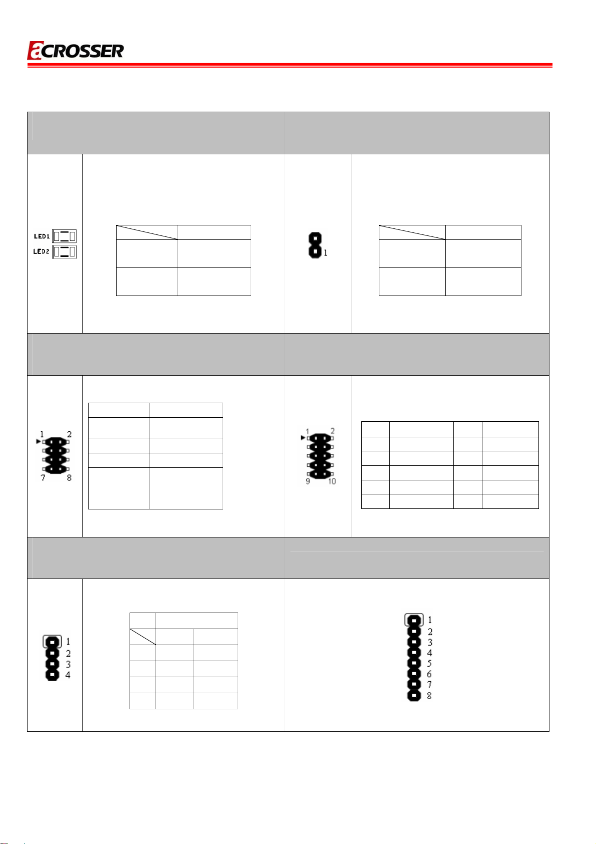
2.3 Connector and Jumper Setting Table
AR-B8172 User Manual
2.1 LED1/LED2 (On-board)
On-board Power/IDE (CF) status LED.
FUNCTION
LED1
( Green)
LED2
(Yellow)
POWER LED
IDE/CF LED
2.3 JP1
COM2 RS-232/42/485 selection and RS-485
termination resistor.
JUMPE UNCTR F ION
2.2 LED3/LED4
Power/IDE (CF) status LED external 2.54mm
1×2PIN connector.
FUNCTION
LED4
( POWER LED)
LED3
( IDE/CF LED)
PIN1 : VCC+
PIN2 : LED Signal
PIN1 : VCC+
PIN2 : LED Signal
1.4 COM2
COM2 RS-232 2.54mm 2×5PIN Connector
1-2 (de RS232 fault)
3-4 RS422
5-6 RS485
7-8
120Ω
TERMIN
ENABL
ATION
E
2.5 CN7
RS422/485 connector (signal from
COM2).NOTE1
PIN SIGNAL
RS485 RS422
1
485D+ 422TX+
2
485D- 422TX-
3
N.C 422RX+
4
N.C 422RX-
PIN SIGNAL PIN SIGNAL
1 DCD 2 DSR
3 RXD 4 RTS
5 TXD 6 CTS
7 DTR 8 RI
9 GND 10 N.C
2.6 CN3 (reserved)
12
Page 13
AR-B8172 User Manual
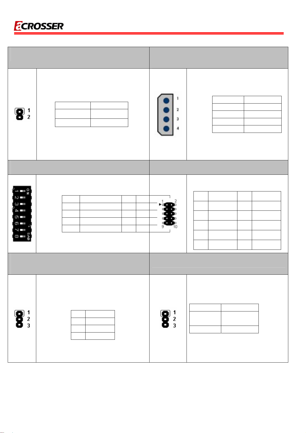
2.7 RST_BTN1
System reset button (2.54mm 1×2PIN connector )
RST_BTN1 FUNCTION
SHORT RESET
OPEN NORMAL
2.9 SW4
SRAM address selection switch
PIN FUCT FUCTIION PIN ON
1 SRAMSEG EL0 LD_ADR2 _S 5 CP
2 SRAMSEG EL1 LD_ADR3 _S 6 CP
3 CPLD_A 0 DR 7 ENA_SRAM
4 CPLD_A 1 Reserve DR 8
2.8 PWR1
AT power input
2.10-11 CN1/CN2
USB 0/1 & 3/4 connector
PIN SIGNAL PIN SIGNAL
1 +5V 2 +5V
3 D0- 4 D1-
5 D0+ 6 D1+
7 GND 8 GND
9 GND 10 GND
PIN SIGNAL
1 +12V
2 GND
3 GND
4 +5V
2.12 CN4
External buzzer connector (signal shared from
BZ1)
PIN FUNCTION
1 VCC
2 BZ-
3 BZ-
2.13 JP2
Clear CMOS data
JUMPE FUNCTR ION
(defau
1-2
lt)
2-3 Clea
NORM
AL
r CMOS
13
Page 14

AR-B8172 User Manual
2.14 A TX1
ATX power supply connector
PIN L SIGNA
1 N PSO
2 B 5VS
3 V +5
1. For ATX power supply, please connect to
ATX1 connector to power supply.
2. For AT power, shorted PIN 2-3 directly then
turn-on power supply to boot-up
2.16 GPIO1
GPIO 0/1 connector
2.15 A TX_BTN1
ATX power-on button
RST_BTN1 FUNCTION
butto
r
n
SHORT
OPEN l Norma
ATX po we
PIN FUNCTION PIN FUNCTION
1 GPIO00 2 GPIO07
3 GPIO01 4 GPIO06
5 GPIO02 6 GPIO05
7 GPIO03 8 GPIO04
9 GND 10 +3.3V
11 GPIO10 12 GPIO17
13 GPIO11 14 GPIO16
15 GPIO12 16 GPIO15
17 GPIO13 18 GPIO14
19 GND 20 +3.3V
14
Page 15

AR-B8172 User Manual
SRAM Access Configuration:
1. Enable SRAM access: SW4.PIN7 is “OFF” to Enable SRAM. If PIN7 is “On” then SRAM
access will be disable.
SW4 Logical description
OFF H
ON L
2. SRAM Address Selection:
SRAM Start Address SRAMSEG_SEL0 SRAMSEG_SEL1
D000:0000 L L
D400:0000 H H
D800:0000 H L
DC00:0000 L H
2. Device IO Address Selection:
Device IO Address CPLD_ADR3 CPLD_ADR2 CPLD_ADR1 CPLD_ADR0
200h L L L L
214h L L L H
2A4h L L H L
2F4h L L H H
2C0h L H L L
2C4h L H L H
2D0h L H H L
2D4h L H H H
2E0h H L L L
2E4h H L H L
3. RAM is 512KB with 32 banks, each bank is 16KB size.
※ Others mode not descript on the above tables are reserved.
15
Page 16

AR-B8172 User Manual
NOTE1:
COM2 RS-232 signals is shared with RS-422/485 (connector is CN7). RS-485 supports
10 nodes with two 120ohm termination resisters:
16
Page 17

AR-B8172 User Manual
3
This chapter describes the BIOS menu displays and explains how to perform common tasks
needed to get the system up. It also gives detailed explanation of the elements found in each of the
BIOS menus. The following topics are covered:
Main Setup
Advanced Setup
PCIPnP Setup
Boot Setup
Security Setup
Chipset Setup
Exit Setup
BIOS SETTING
17
Page 18

3.1 Main Setup
3.1.1 AMI BIOS
This is the interface of AMI BIOS:
AR-B8172 User Manual
3.1.2 Processor
This part shows the auto-detected CPU specification. DM&P Semiconductor is the
Vortex86SX 32-Bit Microprocessor, DDR2 128MB onboard, which is based on x86 structure. It is
the x86 SoC (System on Chip) with 0.13 micron process and ultra low power consumption design
(less than 1 watt)The CPU on the Vortex86SX is a high performance and fully static 32-bit X86
processor with the compatibility of Windows based, Linux and most popular 32-bit RTOS.
3.1.3 System Memory
This part shows the auto-detected system memory. The Vortex86DX is a high performance
with 256MB RAM and speed 133MHz onboard and fully static 32-bit x86 processor, which is
compatible with DOS and Linux. It integrates 32KB write through direct map L1 cache, PCI Rev.
2.1 32-bit bus interface at 33 MHz, SDRAM, DDR2, ROM controller, IPC (Internal Peripheral
Controllers with DMA and interrupt timer/counter included), Fast Ethernet MAC, FIFO UART,
USB2.0 Host and IDE controller into a System-on-Chip (SoC) design. The Vortex86DX are all
256MB onboard and the speed is 133MHz.
3.1.4 System Time:
The time format is based on the 24-hour military time clock. Press the “+” or “–“ key to
increment the setting or type the desired value into the field.
3.1.5 System Date:
Press the “+” or ” –“ to set the date you wanted. The BIOS determines the day of the week
from the other date information; this field is for information only.
18
Page 19
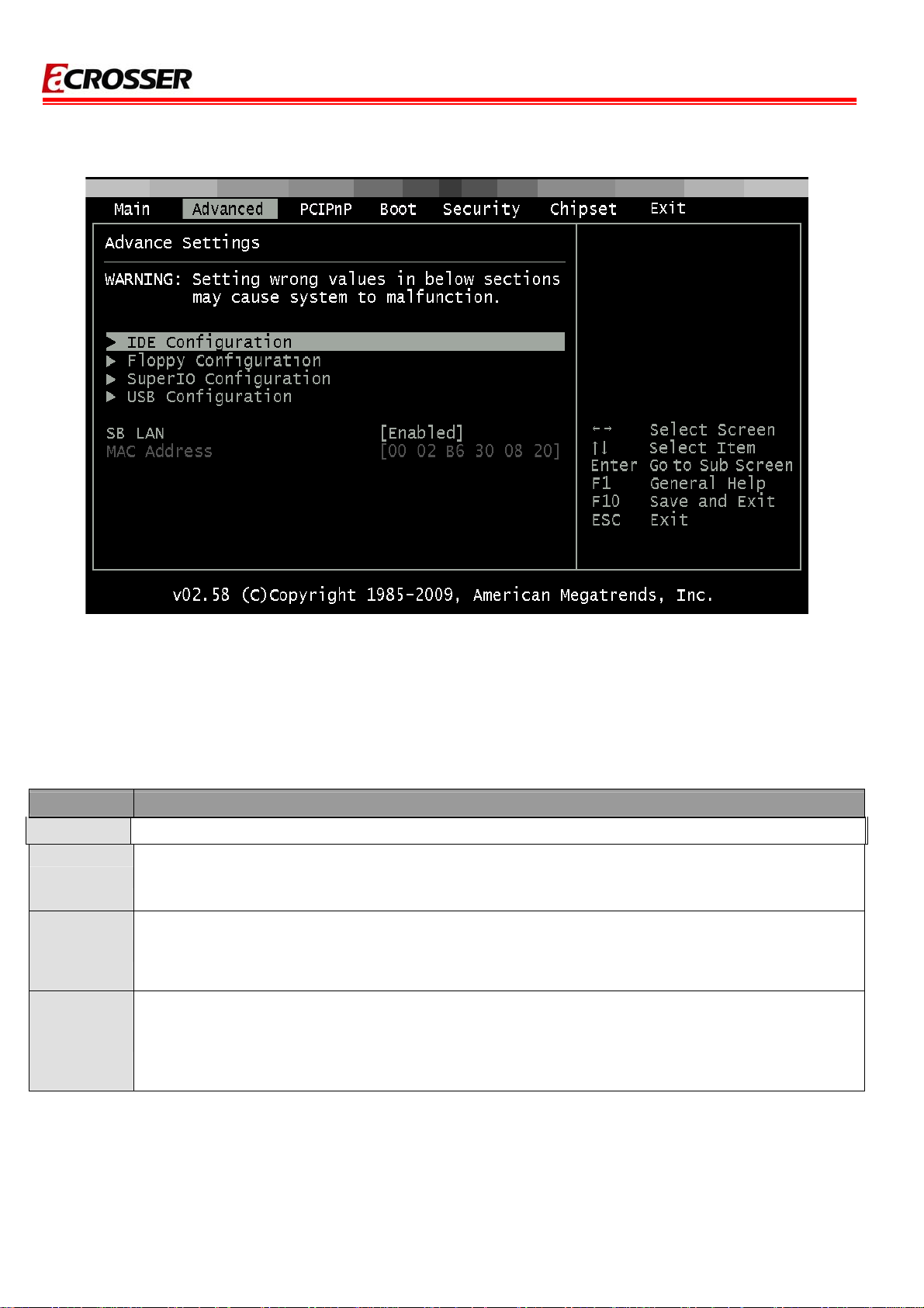
3.2 Advanced Setup
AR-B8172 User Manual
3.2.1 IDE Configuration
OnBoard PCI IDE Controller
This can select the specification you wanted for the IDE device. This option specifies the channel
used by IDE controller on the motherboard,
Option Description
Disabled
Primary
Secondary
Both
Primary IDE Master/Slave
When you entered the IDE devices, the bios will auto-detected and show the detail information of
IDE devices. If you want to change IDE configuration, select the item and press the “Enter” to
configure the item you wanted.
Set this value to prevent the computer system from using the onboard IDE controller.
Set this value to allow the computer system to detect only the Primary IDE channel.
This includes both the Primary Master and the Primary Slave.
Set this value to allow the computer system to detect only the Secondary IDE channel.
This includes both the Secondary Master and the Secondary Slave.
Set this value to allow the computer system to detect the Primary and Secondary IDE
channels.
This includes the Primary Master, Primary Slave, Secondary Master, and Secondary
Slave. This is the default setting.
19
Page 20

AR-B8172 User Manual
3.2.3 SuperIO Configuration
You can use this screen to select options for the Super I/O settings. Use the up and down
<Arrow> keys to select an item. Use the <Plus> and <Minus> keys to change the value of the
selected option. The settings are described on the following pages. The screen is shown below.
Onboard Floppy Controller
This item specifies the Floppy used by the onboard Floppy controller. The settings are Disabled or
Enabled.
Floppy Drive Swap
This option allows you to Enabled or Disabled the Floppy Drive Swap.
3.2.4 USB Configuration
USB Functions
Set this value to allow the system to enable or disable the onboard USB ports. The Optimal and
Fail-Safe default setting is Enabled.
Option Description
Disabled
Enabled
Legacy USB Support
Legacy USB Support refers to the USB mouse and USB keyboard support. Normally if this option
is not enabled, any attached USB mouse or USB keyboard will not become available until a USB
compatible operating system is fully booted with all USB drivers loaded. When this option is
enabled, any attached USB mouse or USB keyboard can control the system even when there is no
USB drivers loaded on the system. Set this value to enable or disable the Legacy USB Support.
The Optimal and Fail-Safe default setting is Disabled.
Option Description
Disabled
Enabled
This setting makes the onboard USB ports unavailable.
This setting allows the use of the USB PORTS. This is the default setting.
Set this value to prevent the use of any USB device in DOS or during system
boot. This is the default setting.
Set this value to allow the use of USB devices during boot and while using DOS.
Auto
This option auto detects USB Keyboards or Mice and if found, allows them to be
utilized during boot and while using DOS.
20
Page 21
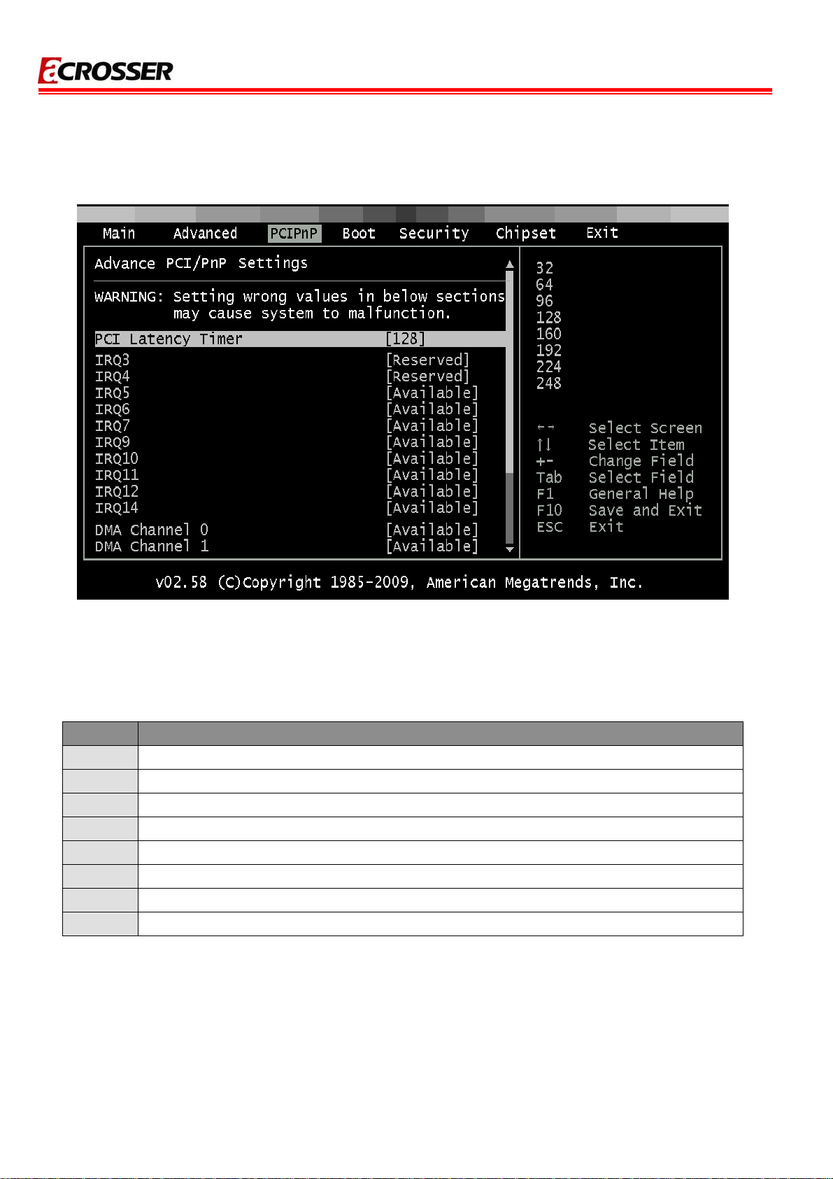
3.3 PCIPnP
3.3.1 Clear NVRAM
Clear NVRAM during system boot.
AR-B8172 User Manual
3.3.2 PCI Latency Timer
Allow you to select the value in units of PCI clocks for all of the PCI device latency timer
register. Configuration option: 32, 64, 96, 128, 160, 192, 224, 248.
Option Description
32
64
96
128
160
192
224
248
Set this value to allow the PCI Latency Timer to be adjusted. This option sets the latency of all
PCI devices on the PCI bus This decides how long a PCI device can hog the PCI bus for , higher
setting , hogs the bus a little longer , lower setting lets go quicker but stuff like some sound card
(PCI of course) will start to crackle , default on this board was default at 64.
This option sets the PCI latency to 32 PCI clock cycles.
This option sets the PCI latency to 64 PCI clock cycles. This is the default setting.
This option sets the PCI latency to 96 PCI clock cycles.
This option sets the PCI latency to 128 PCI clock cycles.
This option sets the PCI latency to 160 PCI clock cycles.
This option sets the PCI latency to 192 PCI clock cycles.
This option sets the PCI latency to 224 PCI clock cycles.
This option sets the PCI latency to 248 PCI clock cycles.
21
Page 22

AR-B8172 User Manual
IRQ
This item can select the IRQ with Available or Reserved. And the default of IRQ3, 4 are Reserved
and others are Available. When you set available, the specified IRQ is to be used by a PCI/PnP
device; as you set reserved, the IRQ will reserved for legacy ISA devices.
Interrupt Option Description
IRQ3
IRQ4
IRQ5
Available
IRQ6
This setting allows the specified IRQ to be used by a PCI/PnP
device. This is the default setting.
IRQ7
IRQ8
IRQ9
IRQ10
IRQ11
IRQ12
Reserved
This setting allows the specified IRQ to be used by a legacy ISA
device.
IRQ13
IRQ14
IRQ15
DMA Channel
This item can select the DMA Channel for Available or Reserved. When set to Available the
specified DMA is available for used by PCI/PnP devices; when set to reserved, the specified DMA
to be used by a legacy ISA device.
DMA Channel Option Description
DMA Channel 0
DMA Channel 1
DMA Channel 3
Available
This setting allows the specified DMA to be used by PCI/PnP
device. It
is
default setting.
DMA Channel 5
DMA Channel 6
Reserved
This setting allows the specified DMA to be used by a legacy ISA
device.
DMA Channel 7
Reserved Memory Size
Set this value to allow the system to reserve memory that is used by ISA devices. The optimal and
Fail-Safe default setting is Disabled.
Option Description
Disabled
16K
32K
64K
Set this value to prevent BIOS from reserving memory to ISA devices.
Set this value to allow the system to reserve 16K of the system memory to the ISA devices.
Set this value to allow the system to reserve 32K of the system memory to the ISA devices.
Set this value to allow the system to reserve 64K of the system memory to the ISA devices.
22
Page 23

AR-B8172 User Manual
3.4 Boot
The Boot menu items allow you to change the system boot options. Select an item then press
Enter to display the sub-menu.
3.4.1 Boot Settings Configuration
Allow you to configure the system boot setting with bellow submenus.
Quick Boot
Set the
to decrease the time needed to boot the system. When you set the value to Disable the BIOS will
performs all the POST items.
Option Description
Disabled
Enabled
PS/2 Mouse Support
Set this value to allow the PS/2 mouse support to be adjusted. The Optimal and Fail-Safe default
setting is Enabled.
Option Description
value to Enable to allow the BIOS to skip some Power On Self Tests (POST) while booting
Set this value to allow BIOS to perform all POST tests.
Set this value to allow BIOS to skip certain POST tests to boot faster.
Disabled
Enabled
This option will prevent the PS/2 mouse port from using system resources and will
prevent the port from being active. Use this setting if installing a serial mouse.
Set this value to allow the system to use a PS/2 mouse. This is the default setting.
23
Page 24

AR-B8172 User Manual
Hit “DEL” Massage Display
Set this value to allow the Hit “DEL” to enter Setup Message Display to be modified. The Optimal
and Fail-Safe default setting is Enabled.
Option Description
Disabled
Enabled
This prevents the export to display Hit Del to enter Setup during memory initialization. If
Quiet Boot is enabled, the Hit 'DEL' message will not display.
This allows the export to display Hit Del to enter Setup during memory initialization.
This is the default setting.
24
Page 25

AR-B8172 User Manual
3.5 Security
The Security menu items allow you to change the system security settings. Select an item then
press Enter to display the configuration options.
Supervisor Password
Indicate whether a supervisor password has been set. If the password has been installed,
Installed displays. If not, Not Installed displays.
Change Supervisor Password
Select this option and press <Enter> to access the sub menu. You can use the sub menu to
change the supervisor password. Select Change Supervisor Password from the Security Setup
menu and press <Enter>. Enter New Password: appears. Type the password and press <Enter>.
The screen does not display the characters entered. Retype the password as prompted and press
<Enter>. If the password confirmation is incorrect, an error message appears. The password is
stored in NVRAM.
Change User Password
Select this option and press <Enter> to access the sub menu. You can use the sub menu to
change the user password.
Clear User Password
Select this option and press <Enter> to access the sub menu. You can use the sub menu to clear
the user password. Select Change User Password from the Security Setup menu and press
<Enter>. Enter New Password: appears. Type the password and press <Enter>. The screen does
not display the characters entered. Retype the password as prompted and press <Enter>. If the
password confirmation is incorrect, an error message appears. The password is stored in NVRAM
Clear User Password
Select Clear User Password from the Security Setup menu and press <Enter>. Clear New
Password [Ok] [Cancel] appears. Type the password and press <Enter>. The screen does not
display the characters entered. Retype the password as prompted and press <Enter>. If the
password confirmation is incorrect, an error message appears. The password is stored in NVRAM.
25
Page 26

AR-B8172 User Manual
3.6 Chipset Setup
3.6.1 SouthBridge Configuration
You can use this screen to select options for the South Bridge Configuration. South Bridge is a
chipset on the motherboard that controls the basic I/O functions. Use the up and down. <Arrow>
keys to select an item. Use the <Plus> and <Minus> keys to change the value of the selected
option.
ISA Configuration
This allows
Serial/Parallel Port Configuration
These options specify the serial port address and the parallel port mode and select the IRQ of
Serial/Parallel Port.
you to set the ISA bus frequency and to select the clock value of I/O and Memory.
Option Description
Disabled
3F8/IRQ4
Set this value to prevent the serial port from accessing any system resources. When
this option is set to disabled, the serial port physically becomes unavailable.
Set this value to allow the serial port to use 3F8 as its I/O port address and IRQ 4 for
the interrupt address. This is the default setting. The majority of serial port 1 or COM1
ports on computer systems use IRQ4 and I/O Port 3F8 as the standard setting. The
most common serial device connected to this port is a mouse. If the system will not use
a serial device, it is best to set this port to disabled.
2F8/IRQ3
Set this value to allow the serial port to use 2F8 as its I/O port address and IRQ 3 for
the interrupt address. If the system will not use a serial device, it is best to set this port
26
Page 27

to disabled.
Set this value to allow the serial port to use 3E8 as its I/O port address and IRQ 4 for
3E8/IRQ4
2E8/IRQ3
the interrupt address. If the system will not use a serial device, it is best to set this port
to disabled.
Set this value to allow the serial port to use 2E8 as its I/O port address and IRQ 3 for
the interrupt address. If the system will not use a serial device, it is best to set this port
to disabled.
Option Description
AR-B8172 User Manual
Normal
Bi-Directional
EPP
EPP
Option Description
5
Set this value to allow the standard parallel port mode to be used. This is the
default setting.
lSet this value to allow data to be sent to and received from the parallel port.
The parallel port can be used with devices that adhere to the Enhanced Parallel
Port (EPP) specification. EPP uses the existing parallel port signals to provide
asymmetric bi-directional data transfer driven by the host device.
The parallel port can be used with devices that adhere to the Extended
Capabilities Port (ECP) specification. ECP uses the DMA protocol to achieve data
transfer rates up to 2.5 Megabits per second. ECP provides symmetric
bi-directional communication.
Set this value to allow the serial port to use Interrupt 3.
Set this value to allow the serial port to use Interrupt 7. This is the default setting.
7
The majority of parallel ports on computer systems use IRQ7 and I/O Port 378H
as the standard setting.
27
Page 28
3.7 Exit
AR-B8172 User Manual
3.7.1 Save Changes and Exit
Once you finished the selections, this option will allow you to determine whether to accept the
modifications or not. Select the “OK” to save the change and exit, if you select “NO”, you will return
to Setup utility.
3.7.2 Discard Change and Exit
Select this option to exit the Setup without saving any change you have made in this session. Press
“OK” will quit the Setup utility without saving any modifications. Press “NO” will return to Setup
utility.
3.7.3 Discard Change
This option allows you to load the default values to your system configuration. These default
settings will save the setup without making any permanent changes to the system configuration.
Discard Changes This option allows you to discard the selections you made and restore the
previously saved value.
3.7.4 Load Optimal Defaults
This option allows you to load the default values to your system configuration. These default
settings are optimal and enable all high performance features.
3.7.5 Load Failsafe Defaults
This option allows you to load the failsafe default values for each of the parameters on the Setup
menus, this will provide the most stable performance setting.
28
Page 29

AR-B8172 User Manual
BIOS REFRESHING, WATCHDOG AND
4
GPIO PROGRAMMING
4.1 BIOS Refreshing
The BIOS program instructions are contained within computer chips called FLASH ROMs that
are located on your system board. The chips can be electronically reprogrammed, allowing you to
update your BIOS firmware without removing and installing chips.
The AR-B8172 provides the FLASH BIOS update function for you to easily to update BIOS. Please
follow these operating steps to update BIOS:
STEP1 You must boot up system into MS-DOS first and please don’t detect files CONFIG.SYS
and AUTOEXEC.BAT.
STEP2 In the MS-DOS mode, you should execute the AMIFLASH program to update BIOS.
STEP3 Follow all messages then you could update BIOS smoothly.
4.2 WATCHDOG Programming
This section describes the usage of WatchDog. AR-B8172 integrated the WatchDog that
enable user to reset the system after a time-out event. User can use a program to enable the
WatchDog and program the timer in range of 1~255 second(s)/minute(s). Once user enables the
WatchDog, the timer will start to count down to zero except trigger the timer by user’s program
continuously. After zeroize the timer (stop triggering), the WatchDog will generate a signal to reset
the system. It can be used to prevent system crash or hang up. The WatchDog is disabled after
reset and should be enabled by user’s program.
Please refer to the following table to program WatchDog properly, and user could test
WatchDog under ‘Debug’ program
WatchDog demo program in Turbo C++ as following:
//===========================================================================
// Turbo C++ Version 3.0 Copyright(c) 1990, 1992 by Borland International,Inc.
//===========================================================================
// Describe : Vortex86DX WatchDog timer test
// Date : 09/16/2009
// Author : Willy
//===========================================================================
//===========================================================================
// Language include files
//===========================================================================
#include <conio.h>
#include <stdlib.h>
#include <stdio.h>
29
Page 30

AR-B8172 User Manual
#include <dos.h>
//===========================================================================
// Normal procedure
//===========================================================================
void Show_Help();
//===========================================================================
// Main procedure
//===========================================================================
int main(int argc, char *argv[])
{
unsigned char IO_Port_Address=0x22; // Index Port 22h, Date Port 23h
unsigned char Signal;
unsigned char Time;
unsigned long Timer;
unsigned char Counter0;
unsigned char Counter1;
unsigned char Counter2;
int Temp;
if ( argc != 3 )
{ Show_Help(); return 1; }
clrscr();
Signal=atoi(argv[1]); // Signal Set Bits
Signal=Signal<<4;
Time=atoi(argv[2]); // Watchdog counter
Timer=Time*32768;
Counter0=(unsigned char)Timer;
Counter1=(unsigned char)(Timer>>8);
Counter2=(unsigned char)(Timer>>16);
// Select Watchdog Signal Source
outportb(IO_Port_Address,0x38); // WDT0 signal select
outportb(IO_Port_Address+1,Signal);
// Set Watchdog timer
outportb(IO_Port_Address,0x39); // WDT0 Counter0
outportb(IO_Port_Address+1,Counter0);
outportb(IO_Port_Address,0x3A); // WDT0 Counter1
outportb(IO_Port_Address+1,Counter1);
outportb(IO_Port_Address,0x3B); // WDT0 Counter2
outportb(IO_Port_Address+1,Counter2);
// Set Watchdog Enabled.
outportb(IO_Port_Address,0x37); // WDT0 Enabled Control Reg.
outportb(IO_Port_Address+1,0x40);
textcolor(YELLOW);
for(Temp=Time;Temp>0;Temp--)
{
gotoxy(20,10);
if(Signal==0xD0)
cprintf(">>> After %3d Second will reset the system. <<<",Temp);
else
cprintf(">>> After %3d Second Watchdog Signal will occur. <<<",Temp);
30
Page 31

AR-B8172 User Manual
delay(1000);
}
textcolor(LIGHTRED);
gotoxy(18,10);
if(Signal==0xD0)
cprintf("If you can see this message, Reset system is Fail");
else
cprintf("If you can see this message, Watchdog Signal is occur.");
return 1;
}
//===========================================================================
// Function : Show_Help()
// Input : -
// Change : -
// Return : -
// Description : Show Title string.
//===========================================================================
void Show_Help()
{
clrscr();
printf("WatchDog Test for Vortex86DX \n\n");
printf("Signal Select \n");
printf("1 : IRQ3 2 : IRQ4 4 : IRQ5 \n");
printf("4 : IRQ6 5 : IRQ7 6 : IRQ9 \n");
printf("7 : IRQ10 8 : IRQ11 9 : IRQ12\n");
printf("10: IRQ14 11: IRQ15 12: NMI \n");
printf("13: System Reset \n\n");
printf("Sample: \n");
printf(" WDT.EXE 1 10 \n");
printf("For 10 seconds to IRQ3. \n\n");
printf(" WDT.EXE 13 10 \n");
printf("For 10 seconds to system reset.\n");
}
31
Page 32
AR-B8172 User Manual
4.3 GPIO Programming
Data Port
(GPIO0 Base Address 0 Refers to the Register of index 61h-60h, IDSEL = AD18/SB of PCI
Configuration Register)
(GPIO1 Base Address 1 Refers to the Register of index 63h-62h, IDSEL = AD18/SB of PCI
Configuration Register)
(GPIO2 Base Address 2 Refers to the Register of index 65h-64h, IDSEL = AD18/SB of PCI
Configuration Register)
(GPIO3 Base Address 3 Refers to the Register of index 67h-66h, IDSEL = AD18/SB of PCI
Configuration Register)
(GPIO4 Base Address 4 Refers to the Register of index 69h-68h, IDSEL = AD18/SB of PCI
Configuration Register)
IO Address Register Name
BA[0] + 00h
BA[1] + 00h
BA[2] + 00h
BA3 + 00h
BA4 + 00h
Direction Port
(Base Address Refers to the Register of index 6Bh-6Ah, IDSEL = AD18/SB of PCI Configuration
Register)
IO Address Register Name
BA + 00h
BA + 01h
BA + 02h
BA + 03h
BA + 04h
BA + 06h
BA + 07h
GPIO PORT0 Data Register
GPIO PORT1 Data Register
GPIO PORT2 Data Register
GPIO PORT3 Data Register
GPIO PORT4 Data Register
GPIO PORT0 Data Register
GPIO PORT1 Data Register
GPIO PORT2 Data Register
GPIO PORT3 Data Register
GPIO PORT4 Data Register
GPIO PORT1 Interrupt Status Register
GPIO PORT0 Interrupt Status Register
32
Page 33

AR-B8172 User Manual
GPIO demo program in Turbo C++ as following:
//===========================================================================
// Turbo C++ Version 3.0 Copyright(c) 1990, 1992 by Borland International,Inc.
//===========================================================================
// Describe : GPIO00~GPIO07 GPIO10~GPIO17 Test utility for Vortex86DX.
// Date : 09/17/2009
// Author : Willy
//===========================================================================
//===========================================================================
// Language include files
//===========================================================================
#include <conio.h>
#include <stdio.h>
//===========================================================================
// Normal procedure
//===========================================================================
void Show_Help();
void Show_Fail();
void Show_Pass();
//===========================================================================
// Main procedure
//===========================================================================
int main(int argc)
{
char *Model_Name="AR-B8172";
unsigned char IO_PORT_BASE=0x22; // DATA_PORT = IO_PORT_BASE + 1;
unsigned char data;
int result=0;
if ( argc >1 )
{ Show_Help(); return 1; }
clrscr();
textcolor(WHITE);
gotoxy(1, 1);
cprintf("<>==========================================================================<>");
gotoxy(1, 2); cprintf("|| Vortex86DX GPIO Test Utility v1.0 Acrosser Technology Co., Ltd. ||");
gotoxy(1, 3);
cprintf("<>==========================================================================<>");
gotoxy(1, 4);
cprintf("<>==========================================================================<>");
gotoxy(1, 5); cprintf("|| Model Name : ||");
gotoxy(1, 6); cprintf("|| SIO IO Base : ||");
gotoxy(1, 7);
cprintf("<>==========================================================================<>");
// Show Got Parameter Informat
textcolor(LIGHTGRAY);
gotoxy(18,5); cprintf("%s",Model_Name);
gotoxy(18,6); cprintf("%X",IO_PORT_BASE);
// Set GPIO00~07 to Output
outportb(IO_PORT_BASE,0x4E);
outportb(IO_PORT_BASE+1,0xFF); // bit=1 , output
// Set GPIO10~GPIO17 to Input
outportb(IO_PORT_BASE,0x4F);
outportb(IO_PORT_BASE+1,0x00); // bit=0 , input
// Set GPIO00~07 to AA
33
Page 34

AR-B8172 User Manual
outportb(IO_PORT_BASE,0x47);
outportb(IO_PORT_BASE+1,0xAA);
// Read GPIO10~17 Status, if not AA error.
outportb(IO_PORT_BASE,0x4C);
if(inportb(IO_PORT_BASE+1)!=0xAA)
result=1;
// Set GPIO00~07 to 55
outportb(IO_PORT_BASE,0x47);
outportb(IO_PORT_BASE+1,0x55);
// Read GPIO10~17 Status, if not 55 error.
outportb(IO_PORT_BASE,0x4C);
if(inportb(IO_PORT_BASE+1)!=0x55)
result=2;
// Set GPIO10~GPIO17 to Output
outportb(IO_PORT_BASE,0x4F);
outportb(IO_PORT_BASE+1,0xFF); // bit=1 , output
// Set GPIO00~07 to Input
outportb(IO_PORT_BASE,0x4E);
outportb(IO_PORT_BASE+1,0x00); // bit=0 , input
// Set GPIO10~17 to AA
outportb(IO_PORT_BASE,0x4D);
outportb(IO_PORT_BASE+1,0xAA);
// Read GPIO00~07 Status, if not AA error.
outportb(IO_PORT_BASE,0x46);
if(inportb(IO_PORT_BASE+1)!=0xAA)
result=3;
// Set GPIO10~17 to 55
outportb(IO_PORT_BASE,0x4D);
outportb(IO_PORT_BASE+1,0x55);
// Read GPIO00~07 Status, if not 55 error.
outportb(IO_PORT_BASE,0x46);
if(inportb(IO_PORT_BASE+1)!=0x55)
result=4;
if(result)
Show_Fail();
else
Show_Pass();
return result;
}
//===========================================================================
// Function : Show_Help()
// Input : -
// Change : -
// Return : -
// Description : Show Title string.
//===========================================================================
void Show_Help()
{
clrscr();
printf("GPIO Test utility for Vortex86DX\n\n");
printf("GPIO00 迋? VCC \n");
34
Page 35

AR-B8172 User Manual
printf("GPIO01 迋迋? 奼迋迋迋? GPIO07\n");
printf("GPIO02 迋迋迋? ?奼迋迋? GPIO06\n");
printf("GPIO03 迋迋迋迋? ??奼迋? GPIO05\n");
printf("GND ???? ???奼? GPIO04\n");
printf("GPIO10 迋???? ???? VCC \n");
printf("GPIO11 迋迋??? 迋迋迋? GPIO17\n");
printf("GPIO12 迋迋迋?? 迋迋? GPIO16\n");
printf("GPIO13 迋迋迋迋? 迋? GPIO15\n");
printf("GND ? GPIO14\n");
}
//===========================================================================
// Function : Show_Fail()
// Input : -
// Change : -
// Return : -
// Description : Show Fail Message.
//===========================================================================
void Show_Fail()
{
textcolor(LIGHTRED);
gotoxy(20,10); cprintf(" 詗詗詗詗 詗詗詗 詗詗 詗 ");
gotoxy(20,11); cprintf(" 詗 詗 詗 詗 詗 ");
gotoxy(20,12); cprintf(" 詗詗詗? 詗詗詗詗 詗 詗 ");
gotoxy(20,13); cprintf(" 詗 詗 詗 詗 詗 ");
gotoxy(20,14); cprintf(" 詗 詗 詗 詗詗 詗詗詗詗");
}
//===========================================================================
// Function : Show_Pass()
// Input : -
// Change : -
// Return : -
// Description : Show Pass Message.
//===========================================================================
void Show_Pass()
{
textcolor(LIGHTGREEN);
gotoxy(20,10); cprintf(" 詗詗詗詗 詗詗詗 詗詗詗詗 詗詗詗詗");
gotoxy(20,11); cprintf(" 詗 詗 詗 詗 詗 詗 ");
gotoxy(20,12); cprintf(" 詗詗詗詗 詗詗詗詗 詗詗詗詗 詗詗
gotoxy(20,13); cprintf(" 詗 詗 詗 詗 詗");
gotoxy(20,14); cprintf(" 詗 詗 詗 詗詗詗詗 詗詗詗詗");
詗詗");
35
Page 36

AR-B8172 User Manual
5
ELECTRICAL CHARACTERISTICS
5.1 Basic Electrical Characteristics Table
Electrical Characteristics
Symbol Parameter / Condition
Min. Typ. Max.
TA Ambient Temperature
Tstg Storage Temperature
+12V External power input for system or +12Vdc power output 11.4 12.0 12.6 V
+5V +5Vdc power input 4.75 5.0 5.25 V
GPIO VIL GPIO’s maximum Input LOW voltage - 0 0.8 V
GPIO VIH GPIO’s minimum input HIGH voltage 2.5 3.3 - V
GPIO VOL GPIO’s typical output LOW voltage - - 0.4 V
-20 - 80 ℃
Value
0 - 60 ℃
Unit
GPIO VOH GPIO’s typical output HIGH voltage 2.4 - - V
36
 Loading...