

Page 1

AR-B6051 Board
User Manual
1
Page 2

Copyright
All Rights Reserved.
Manual’s first edition:
For the purpose of improving reliability, design and function, the information in this document is
subject to change without prior notice and does not represent a commitment on the part of the
manufacturer.
In no event will the manufacturer be liable for direct, indirect, special, incidental, or
consequential damages arising out of the use or inability to use the product or documentation, even
if advised of the possibility of such damages.
This document contains proprietary information protected by copyright. All rights are reserved.
No part of this Manual may be reproduced by any mechanical, electronic, or other means in any
form without prior written permission of the manufacturer.
Trademarks
AR-B6051 are registered trademarks of Acrosser; IBM PC is a registered trademark of the
International Business Machines Corporation; Pentium is a registered trademark of Intel
Technologies Inc; Phoenix is a registered trademark of Phoenix Software International Inc; other
product names mentioned herein are used for identification purposes only and may be
trademarks and/or registered trademarks of their respective companies.
2
Page 3

Table of Contents
Chapter 1 Introduction.................................................................................................................................4
1.1 Specifications.................................................................................................................................4
1.2 Package Contents...........................................................................................................................5
1.3 Block Diagram...............................................................................................................................5
Chapter 2 H/W Information.........................................................................................................................6
2.1 Mainboard illustration (Top Side) .................................................................................................6
2.2 Locations of I/O ports & Jumper settings definition .....................................................................8
Chapter 3 BIOS Settings............................................................................................................................15
3.1 Main Setup...................................................................................................................................16
3.2 Advanced Setup...........................................................................................................................18
3.3 Security Setup..............................................................................................................................19
3.4 Superio Setup...............................................................................................................................20
3.5 Boot setup ....................................................................................................................................22
3.6 Exit Setup.....................................................................................................................................23
Chapter 4 Function Description.................................................................................................................25
4.1 DC Power input connection.........................................................................................................25
4.2 Digital Inputs ...............................................................................................................................25
4.3 Digital Outputs.............................................................................................................................26
4.4 Watchdog Timer ..........................................................................................................................27
4.5 RS-232 Ports................................................................................................................................27
4.6 Serial ATA (SATA).....................................................................................................................28
4.7 USB..............................................................................................................................................28
Chapter 5 Driver And Utility Installation ..................................................................................................29
5.1 Driver CD Interface Introduction.................................................................................................29
Chapter 6 Software Installation and Programming Guide.........................................................................43
6.1 CAN bus.......................................................................................................................................43
6.2 GPIO and Watchdog....................................................................................................................45
6.3 API List and Descriptions............................................................................................................46
6.3.1 CAN Bus.............................................................................................................................46
6.3.2 GPIO and Watchdog...........................................................................................................52
Appendix A................................................................................................................................................55
3
Page 4

Chapter 1 Introduction
Acrosser Technology Co. Ltd, global professional industrial and embedded computer provider,
announces the new 3.5” SBC, AR-B6051, which carries the Intel Atom E640 and E620. It supports
DDR2 memory and capacity is 1GB. It’s the onboard design and it will avoid the risk of vibration and
shock issue. Based on embedded concept, AR-B6051 has variety IO like 4 x serial port, 4 x USB, 2
x GbE and Mini-PCIe expansion. It offers the CF socket that embedded customers used to use, 1x
SATA interface for the customers have large storage capacity request.
There is a Mini-PCIe expansion slot for customer’s expansion. As people know there is rapidly
increasing request in wireless request, so Acrosser provides customer the option and customer can
use the module directly without other carrier board. AR-B6051 also supports the CAN Bus function
that is widely used in the vehicle and industrial applications.
1.1 Specifications
Intel Atom E640 1.0GHz / E620 600MHz
Onboard DDR2 1GB
1 x VGA
1 x LVDS
4 x USB2.0
1 x SATA
1 x CF Type II
4 x COM (3 x RS-232, 1 x RS-232/422/485)
2 x GbE (Intel 82574L)
1 x KB/MS
1 x Mini-PCIe
1 x CAN Bus
8-bit GPIO
4
Page 5

1.2 Package Contents
Check if the following items are included in the package.
Quick Manual
AR-B6051 board
1 x Software Utility CD
1 x Audio 3.5 Phone Cable(190030840-G)
1.3 Block Diagram
5
Page 6
Chapter 2 H/W Information
This chapter describes the installation of AR-B6051. At first, it shows the Function diagram
and the layout of AR-B6051. It then describes the unpacking information which you should read
carefully, as well as the jumper/switch settings for the AR-B6051 configuration.
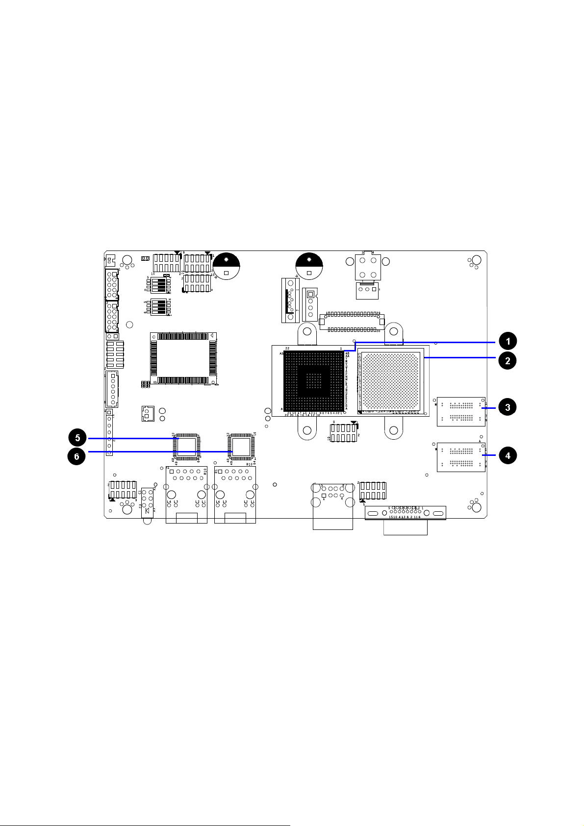
2.1 Mainboard illustration (Top Side)
6
Page 7
Mainboard illustration (Bottom Side)
CPU
Intel ATOM E640 is for AR-B6051E64
Intel ATOM E620 is for AR-B6051E62
Intel PCH E20G DDR2-800 / DRAM3 DDR2-800 / DRAM4
DDR2-800 / DRAM1 DDR2-800 / DRAM2
LAN1
Intel WG82574L / GbE /PCIe
LAN2
Intel WG82574L / GbE /PCIe
7
Page 8
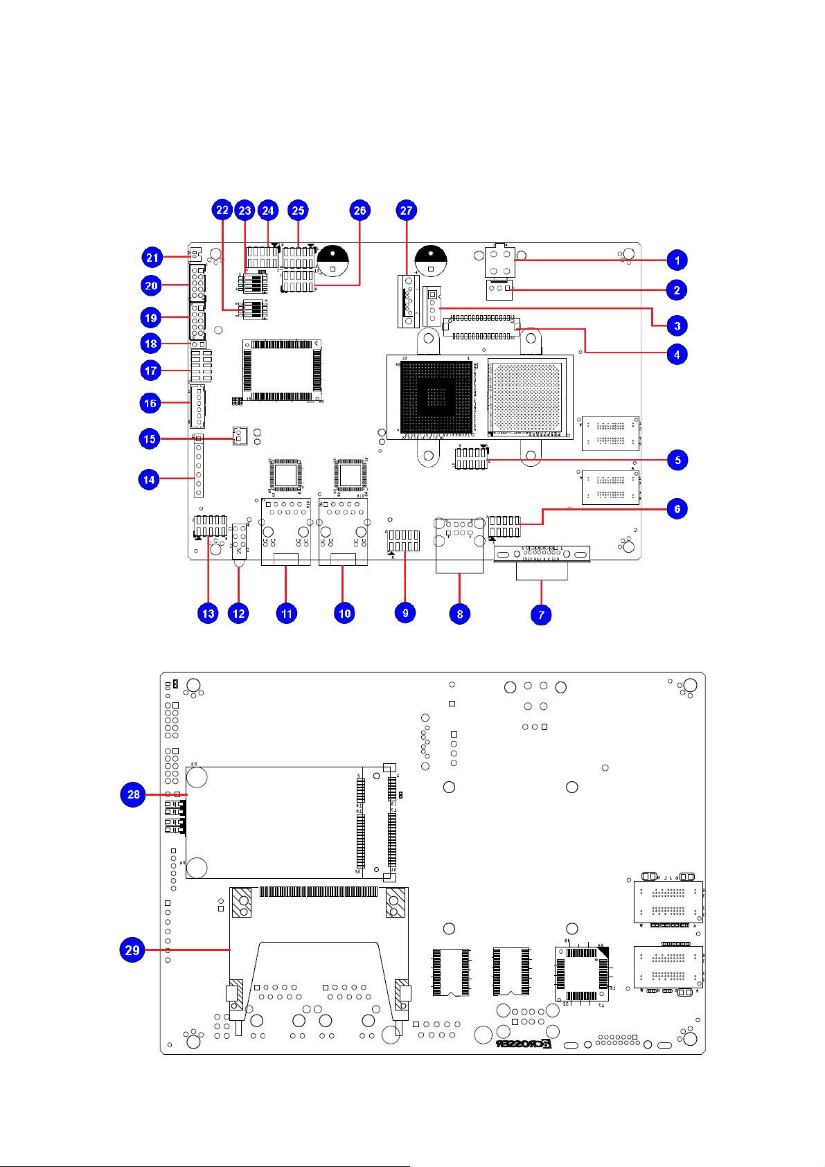
2.2 Locations of I/O ports & Jumper settings definition
TOP SIDE
Bottom SIDE
8
Page 9

ATX12V1
DC +12V Power in
SYS_FAN1
3 pin FAN connector
SATA_PWR1
SATA Power Connector
LVDS1
For LVDS display connector
SPI1
For BIOS Firmware Update
FP_USB1
2x5P 2.0mm pin header for internal
USB Port 3 and Port 4 connector
VGA1
D-SUB VGA Connector
USB1
External USB Port1 and Port 2
connector
COM1
2x5P 2.0mm pin header for COM1
support RS-232 function
LAN2
RJ45 GbE Connector
LAN1
RJ45 GbE Connector
LED1
3 in 1 LED for Power ,CF and SATA
LED
AUDIO1
2x5P 2.0mm pin header for AUDIO
connector.
PIC1
AT/ATX mode selection and for
Power button connection.
CAN1
For CAN bus Connector.
KBMS1
For PS/2 KB and PS/2 Mouse
Connector
GPIO1
2x5P 2.0mm pin header for
4-in/4-out GPIO Connector.
JP1
For COM2 support RS-232 or
RS-422/ RS485 function selected.
RS422_485
2x5P 2.0mm / WAF-JST pin header
support RS-422/485 function
COM2
2x5P 2.0mm / WAF-JST pin header
support RS-232 at COM2
CN_BAT1
WAF-H_1X2P_1.25mm for RTC
Battery connector
SW2
For RS-485 Termination 120 ohm
secretion.
SW1
For RS-422 Termination 120 ohm
secretion.
COM3
2x5P 2.0mm pin header for COM3
support RS-232 function
COM4
2x5P 2.0mm pin header for COM4
support RS-232 function
LPC1
2x5P 2.0mm pin header for LPC
debug card connector.
SATA1
SATA device connector.
MiniPCIe1
Mini-PCIe card device slot.
CF1
CF CARD SOCKET
9
Page 10
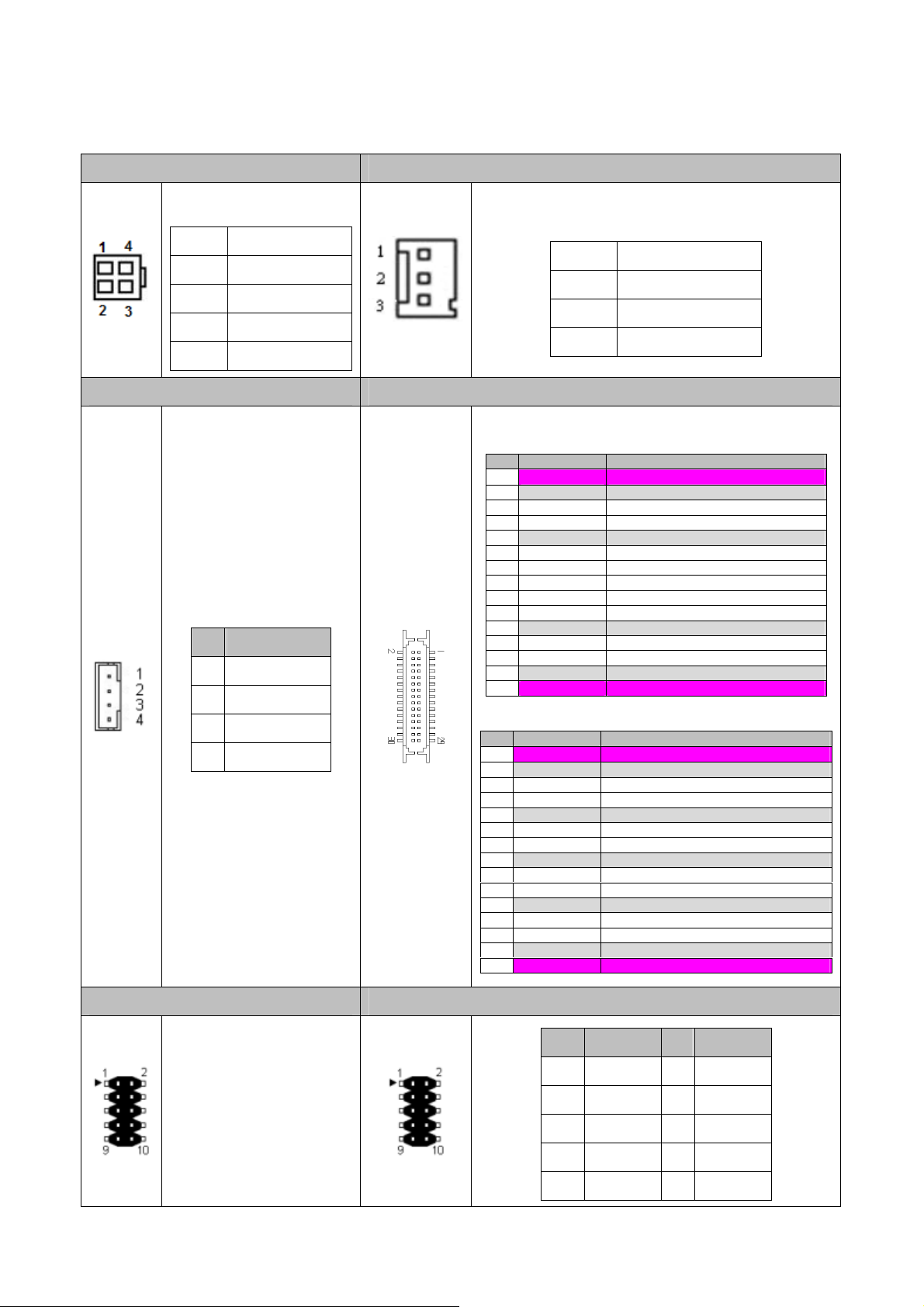
2.21 Connectors and Jumper Settings
1. A TX12V1 2.SYSFAN1
Pin SIGNAL
1 GND
2 GND
3 +12V
4 +12V
3. SATA_PWR1 4. LVDS1
SATA Device Power
Connector
PIN SIGNAL
1
2
3
4
+12V
GND
VCC3
VCC5
Pin SIGNAL
1 GND
2 +12V
3 NC
30 pin DF13 connector
PIN Symbol Description
1 VLED VLED Power
3 Vss Ground
5 VLED_EN LED Enable
7 VPWM_EN System PWM
9 Vss Ground
11 RxIn3+
13 RxIn315 NC No Connected (Reserve)
17 NC No Connected (Reserve)
19 NC No Connected (Reserve)
21 Vss Ground
23 SMB_DATA SMB DATA
25 SMB_CLK SMB CLK
27 Vss Ground
29 VDD Power
PIN Symbol Description
2 VLED VLED Power
4 Vss Ground
6 CKIN+ LVDS receiver signal Clock
8 CKIN- LVDS receiver signal Clock
10 Vss Ground
12 RxIn2+
14 RxIn216 Vss Ground
18 RxIn1+
20 RxIn122 Vss Ground
24 RxIn0+
26 RxIn028 Vss Ground
30 VDD Power
LVDS receiver signal channel 3
LVDS receiver signal channel 3
LVDS receiver signal channel 2
LVDS receiver signal channel 2
LVDS receiver signal channel 1
LVDS receiver signal channel 1
LVDS receiver signal channel 0
LVDS receiver signal channel 0
5. SPI1 ( For BIOS FW Update ) 6. FP_USB1 Connector
Used for BIOS Firmware
Update Tools.
10
PIN SIGNAL PIN SIGNAL
1
3
5
7
9
+5V
Data3-
Data3+
GDN
GDN
2
4
6
8
10
+5V
Data4-
Data4+
GDN
GDN
Page 11
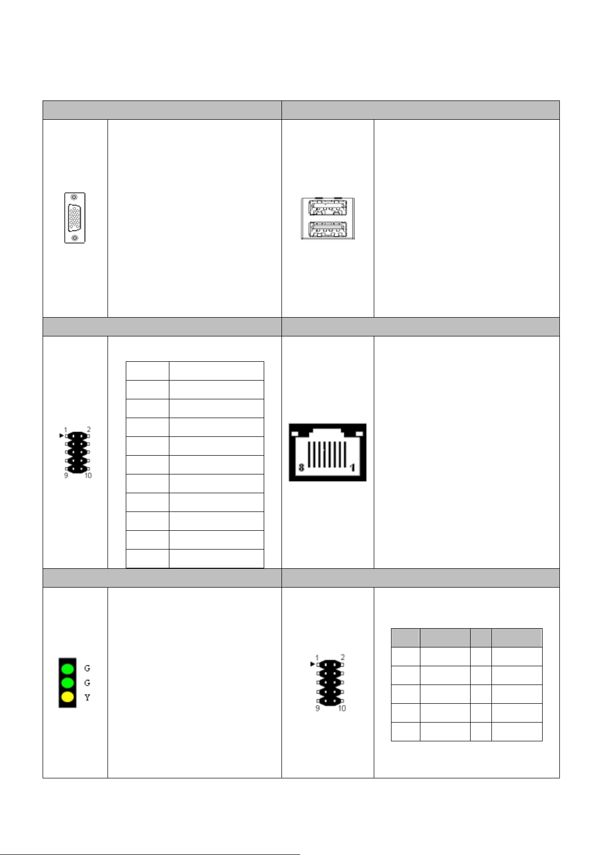
7. VGA1 (D-SUB 15 pin Connector) 8. USB1
D-SUB 15 pin For CRT Monitor
Lower: Port #3.
Upper: Port #4.
9. COM1: Pin header for RS-232 10, 11. LAN1 , LAN2
Pin SIGNAL
1 DSR
2 DCD
3 RTS
4 SIN
5 CTS
6 SOUT
7 RI
RJ45 Ethernet Connector
8 DTR
9 NC
10 GND
12. LED1 13. Audio1
Green : Power ON LED
Green: SATA LED.
Yellow: CF LED
11
PIN SIGNAL PIN SIGNAL
1
3
5
7
9
GND
Line Out_L
GND
Line Out_R
NC
10
GND
2
MIC_L
4
GND
6
MIC_R
8
NC
Page 12
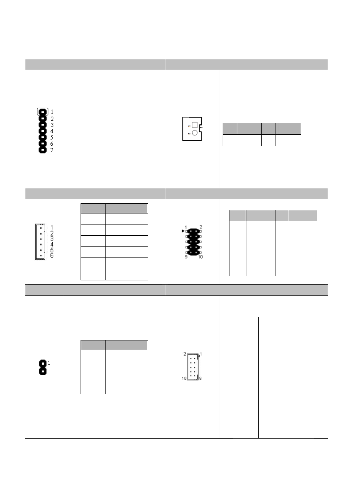
14. PIC1: PIC Programming Connector 15. CAN1: CAN Bus Connector
Pin 1 ~ Pin 5: Reserve
Pin 6 & Pin 7:
- Short: AT Mode.
- Open: ATX Mode
Connect the None-latch type of
button as power button.
Note: The Power Button does support
system shutdown by the button held for
4 seconds on the None-ACPI OS, such
CAN Bus (Controller Area Network)
PIN SIGNAL PIN SIGNAL
1
N ANCA _H
C _L
2
as on MS-DOS.
16. KNMS1: PS/2 KB and PS/2 Mouse 17.GPIO1
PIN SIGNAL
1 MS data
2 KB data
3 GND
4 5V
5 MS clock
6 KB clock
18. JP1: RS-422 or RS485 19. RS422_485
PIN SIGNAL
PIN SIGNAL PIN SIGNAL
GPO 1
1
GPO 2
3
GPO 3
5
GPO 4
7
9
GND
Pin SIGNAL
1 NA
2 485_422_TX2+
2
4
6
8
10
+VCC3
GPI 1
GPI 2
GPI 3
GPI 4
1 - 2
1 - 2
Open (Default)
RS-422
Close
RS-485
3 NA
4 485_422_TX25 422_RX26 NA
7 422_RX2+
8 NA
9 +5V
10 GND
12
Page 13
20. COM2 (For RS-232 Function) 21. CN_BAT1
Pin SIGNAL
1 DSR
2 DCD
3 RTS
4 SIN
5 CTS
6 SOUT
7 RI
8 DTR
9 NC
10 GND
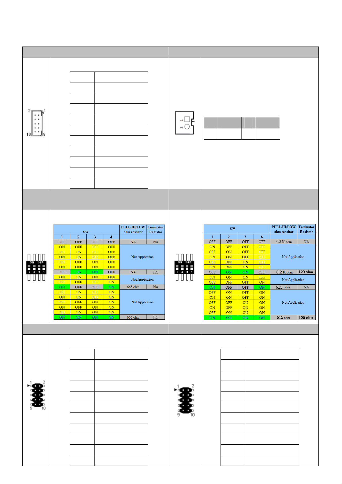
22. SW1: RS-422 RX terminator resistor
selection
Default: All OFF
CAN Bus (Controller Area Network)
PIN S LIGNA PIN S LIGNA
B B -
1
AT+
2
AT
23. SW2: RS-422/485 TX Terminator resistor
selection
Default: All OFF
24. COM3: Pin header for RS-232 25. COM4: Pin header for RS-232
Pin SIGNAL
1 DSR
2 DCD
3 RTS
4 SIN
5 CTS
6 SOUT
7 RI
8 DTR
Pin SIGNAL
1 DSR
2 DCD
3 RTS
4 SIN
5 CTS
6 SOUT
7 RI
8 DTR
9 NC
10 GND
13
9 NC
10 GND
Page 14
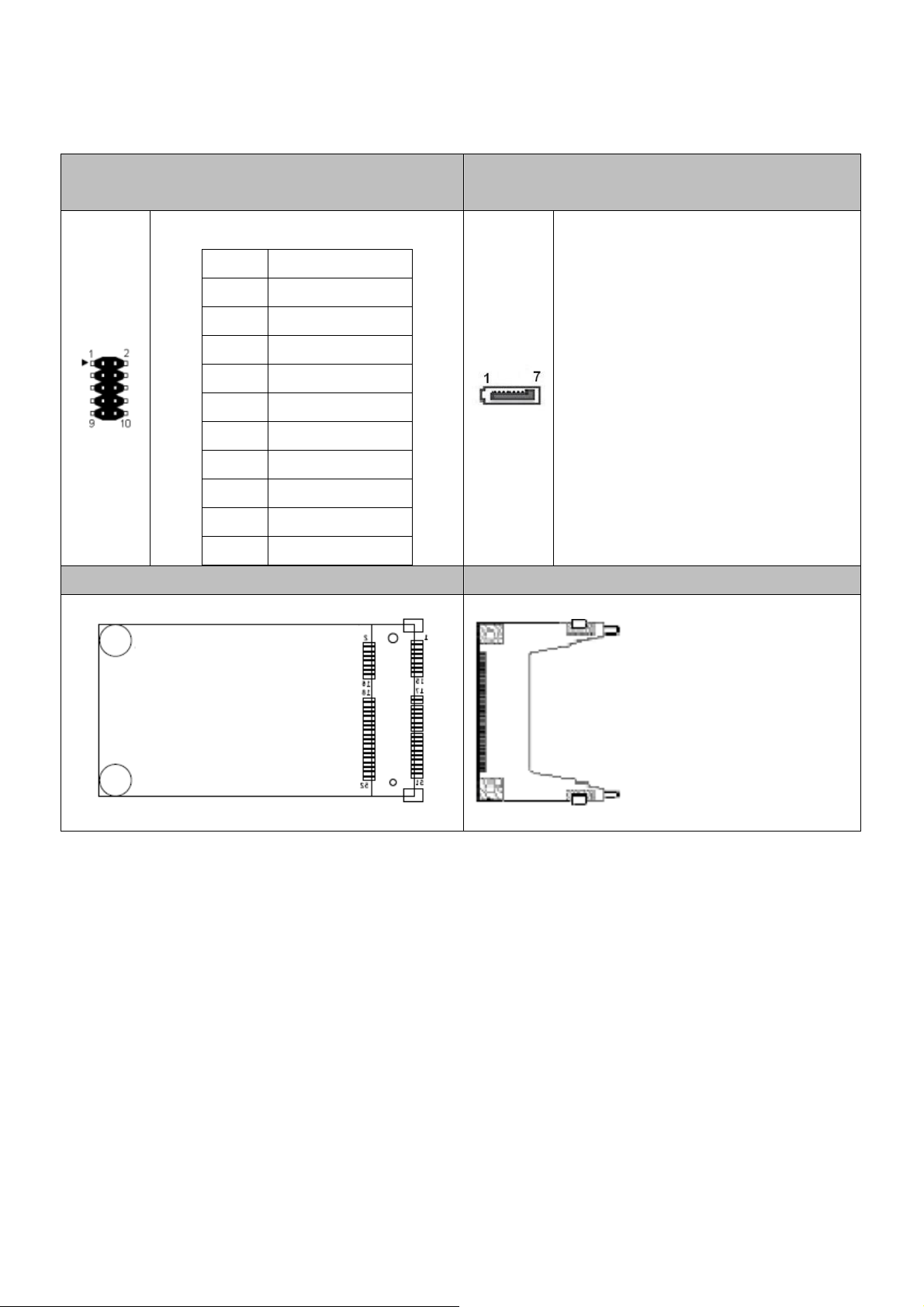
26. LPC1 (LPC BUS Signal Header for Port-80
Debug Tools)
Pin SIGNAL
27. SATA1 (SATA device connector #1)
To connect SATA device:
1 33MHz Clock
1. Attach either end of the signal cable to
2 LAD1
the SATA connector on motherboard.
3 Reset#
4 LAD0
5 LFRAME#
6 VCC3
7 LAD3
8 GND
9 LAD2
10 GND
Attach the other end to the SATA device.
2. Attach the SATA power cable to the
SATA device and connect the other end
from the power supply.
28. MINIPCIE1 ( Mini PCIe Socket ) 29. CF1 (CF CARD Socket)
14
Page 15

Chapter 3 BIOS Settings
This chapter describes the BIOS menu displays and explains how to perform common
tasks needed to get the system up and running. It also gives detailed explanation of the
elements found in each of the BIOS menus. The following topics are covered:
Main Setup
Advanced Setup
Security Setup
Superio Setup
Boot Setup
Exit Setup
15
Page 16
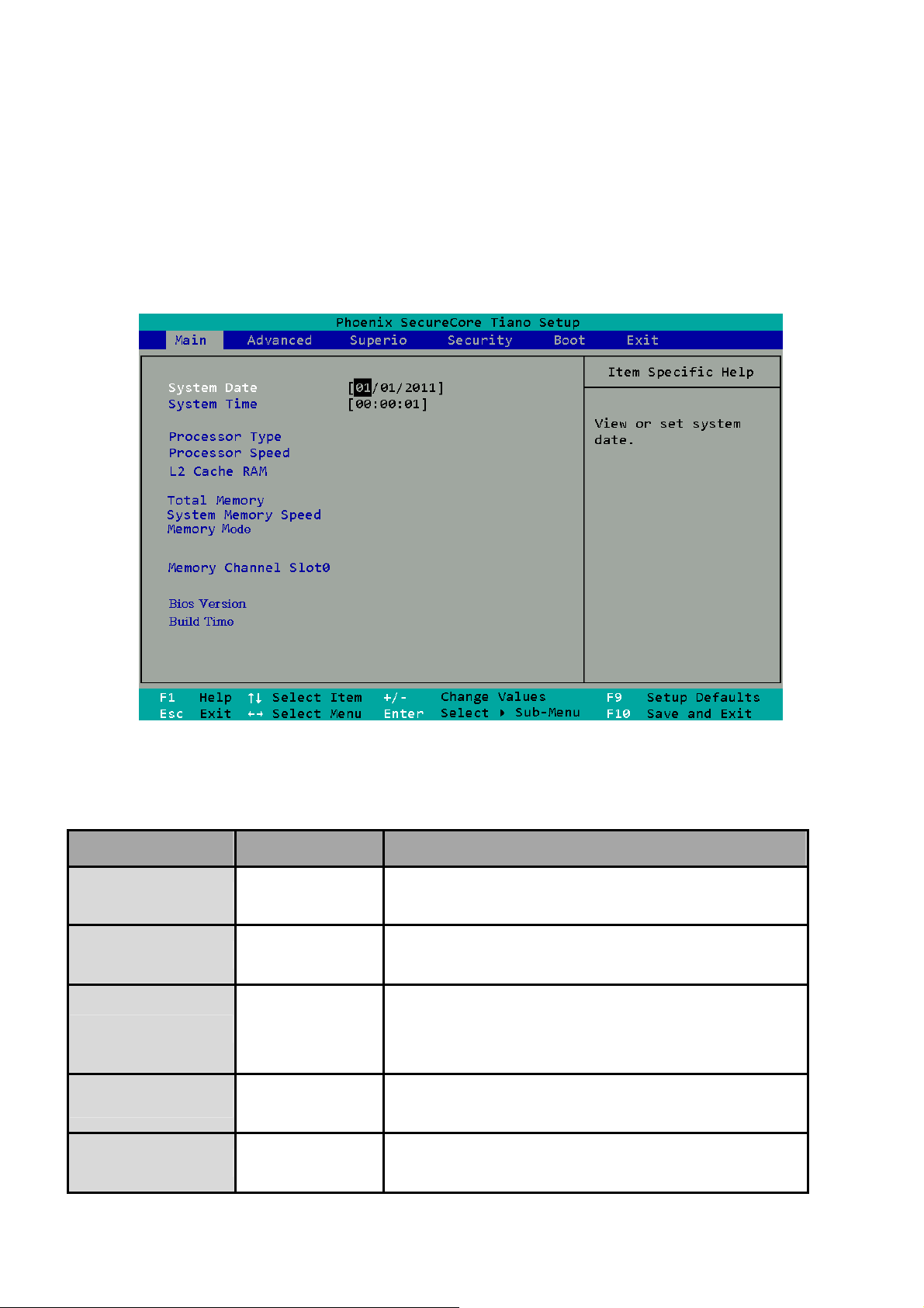
3.1 Main Setup
Once you enter the Phoenix BIOS™ CMOS Setup Utility, the Main Menu will appear on the
screen. Use the arrow keys to highlight the item and then use the <Pg Up> <Pg Dn> keys to
select the value you want in each item.
Note: Listed at the bottom of the menu are the control keys. If you need any help with the item
fields, you can press the <F1> key, and it will display the relevant information.
Option Choice Description
System Date
System Time
Processor Type
Processor Speed
L2 Cache Ram
N/A
N/A Set the system time.
N/A This item displays the CPU Type
N/A This item displays the CPU Speed
N/A This item displays the L2 ache memory size
Set the system date. Note that the ‘Day’ automatically
changes when you set the date
16
Page 17

Total Memory
N/A This item displays the memory size that used.
System Memory
Speed
Memory Mode
Memory Channel slot
0
BIOS Version
Build Time
N/A This item displays the memory speed.
N/A This item displays the memory mode.
N/A This item displays the memory size that used On slot 0.
N/A This item displays BIOS’s Version
N/A This item displays the building time of BIOS.
17
Page 18

3.2 Advanced Setup
Option Choice Description
Full Screen Logo
Show
Quick Boot
Audio
Lan Control 1
Lan Control 2
Enabled
Disabled
Enabled
Disabled
Enable
Disable
Enabled
Disabled
Enabled
Disabled
Displays the full screen logo upon BIOS booting
Allows the system to skip certain tests while booting. This
will decrease the time needed to boot the system.
Control detection of the Azalia device.
Control the Lan1.
Control the Lan2.
Boot Type
LVDS
Select the Video Device activated during POST. When you
LVDS+CRT
select L VDS + CR T then CR T wo uld be main output i n DOS.
CRT
18
Page 19

3.3 Security Setup
Supervisor Password
is
Set Supervisor
Password
The BIOS attempts to load the operating system from the
N/A
devices in the sequence selected in these items.
When a password has been enabled, you will be prompted
to enter your password every time you try to enter Setup.
This prevents unauthorized persons from changing any
part of your system configuration.
Type the p assword, up to eight characters in length, and
Pressing <Enter> on
press <Enter>. The password typed now will clear any
this item for
previous password from the CMOS memory. You will be
confirmation:
asked to confirm the password. Type the password again
and press <Enter>. You may also press <Esc> to abort the
ENTER
selection and not enter a password.
PASSWORD:
To disable a password, just press <Enter> when you are
prompted to enter the password. A message will confirm
that the password will be disabled. Once the password is
disabled, the system will boot and you can enter Setup
freely.
19
Page 20

3.4 Superio Setup
20
Page 21

Option Choice Description
Com_1 2E8/5
Com_2 2F8/7
Com_3 4E8/10
Com_4 4F8/11
CPU Temperature
System Temperature
Enabled
Disabled
Enabled
Disabled
Enabled
Disabled
Enabled
Disabled
N/A
N/A Show you the current system temperature.
Enable or Disable the com port function.
Enable or Disable the com port function.
Enable or Disable the com port function.
Enable or Disable the com port function.
These read-only fields show the functions
of the hardware thermal sensor by CPU
thermal diode that monitors the chip blocks
to ensure a stable system.
CPU VCore
N/A Show you the voltage of Vcore.
21
Page 22

3.5 Boot setup
22
Page 23

3.6 Exit Setup
option Choice Description
Exit Saving
Changes
Exit
Discarding
Changes
Pressing <Enter> on this
Exit BIOS Setup and Save Changes BIOS Setting.
item for confirmation:
Pressing <Enter> on this
Exit BIOS Setup and Without Save Changes BIOS Setting.
item for confirmation:
23
Page 24

When you press <Enter>
on this item you get a
Load Setup
Defaults
Clean CMOS
Discard
Changes
Save
Changes
confirmation dialog box with
a message like this:
Pressing <Enter> on this
item for confirmation:
Pressing <Enter> on this
item for confirmation:
Pressing <Enter> on this
item for confirmation:
Press ‘Y’ to load the default values that are factory-set for
optimal-performance system operations.
Clean CMOS then reboot.
N/A
Save Changes BIOS Setting but without exit BIOS Setup.
24
Page 25

Chapter 4 Function Description
4.1 DC Power input connection
AR-B6051 needs ATX12V to power the board.
4.2 Digital Inputs
There are 4 clamped diode protection digital inputs on GPIO1connector. You can read the
status of any input through the software API. These digital inputs are general purpose input. You
can define their purpose for any digital input function. The detailed information please refers to
Software Programming Guide for how to use the API.
Following diagrams state how to connect the digital inputs to devices on the embedded system.
25
Page 26

4.3 Digital Outputs
There are 4 clamped diode protection digital outputs on GPIO1 connector(pin header). You can
control the output status of these digital outputs through the software API. The four digital
outputs are capable sink maximum 500 mA current for each channel and maximum output
voltage is 12V. The output reference voltage of device, please connect to GPIO1 VCC3V(Pin2).
These digital outputs are general purpose outputs. The detailed information please refers to
Software Programming Guide for how to use the API.
Following diagrams state how to connect the digital outputs to devices on the embedded
system.
Note.
1. Output Default set: Low
2. Output Type: Open drain MOSFET driver
3. It needs a Schottky Diode to parallel connect with any inductive component, such as relay
and bulb.
GPIO1 Pin Define:
PIN SIGNAL PIN SIGNAL
GPO 1
1
GPO 2
3
GPO 3
5
GPO 4
7
9
GND
2
4
6
8
10
+VCC3
GPI 1
GPI 2
GPI 3
GPI 4
26
Page 27

4.4 Watchdog Timer
If you set a watchdog timer, you can use it to reset the system when system hangs up due to
hardware issue. After you set the watchdog timer, the software shall re-set the timer to re-start a
new cycle before it time-out. Please refer to Chapter 6 Software Installation and Programming
Guide for how to set the watchdog timer.
4.5 RS-232 Ports
The COM1/COM2/COM3/COM4 are connected through a cable(pin header). Users need to
plug into RS-232 or RS-422/485 connector. For RS-422/485, please refer to SW1, SW2
setting. The following diagram is their pin definition and signal.
COM1~ COM4: For RS-232 Function
Pin SIGNAL
1 DSR
2 DCD
3 RTS
4 SIN
5 CTS
6 SOUT
7 RI
8 DTR
9 NC
10 GND
27
Page 28

RS422
_485: For RS-422, RS-485
4.6 Serial ATA (SATA)
Pin SIGNAL
1 NA
2 485_422_TX+
3 NA
4 485_422_TX5 422_RX26 NA
7 422_RX2+
8 NA
9 +5V
10 GND
There is one SATA 2.5 ports on the AR-B6051. There is also one SATA power connectors for
the SA TA hard disks. The SAT A power cable is an optional accessory. If you need a SAT A power
connector, please contact your Acrosser sales representative for the quotation.
4.7 USB
There are four USB 2.0 interfaces on the AR-B6051. Two USB connectors are located on the
edge of the board. The other two USB ports are supported by two 2X5 pin internal connector.
You need a special cable for using these two USB ports and they are optional accessories.
Note.
Please use Intel Graphics AP to adjust resolution clone.
28
Page 29

Chapter 5 Driver And Utility Installation
5.1 Driver CD Interface Introduction
Acrosser provides a driver CD, which includes the drivers, utilities, applications and documents.
In Windows environment, it can be guided by the setup program; in Linux environment, the related
files can be found at folder “ARB6051\Linux” in the CD.
Once putting the CD into the optical disk drive, it will run automatically. The driver CD will also
detect the system board information to see if they are matched. The following error messages appear if
you get an incorrect driver CD.
It indicates that the system information is not available.
It indicates that the program gets wrong system information.
29
Page 30

Driver Page
This is the Driver Installation Page.
30
Page 31

Click the icon, all the drivers will be selected.
31
Page 32

Click the icon, all selected items will be cleared.
32
Page 33

Click the icon to install the selected drivers.
The progressing bar shows up. The main window temporarily disappears.
33
Page 34

Please click ‘Yes’ to restart the system.
34
Page 35

Click this icon to browse this CD content.
Utility Page
Acrosser prov
launch this utility.
ides a test utility. Users can double click the item ‘Test Utility’ on the ‘Utility’ page to
35
Page 36

Before launching this utility, users have to install the ‘Acrosser Driver’ in advance. The system may
ask for installing other libraries. You can find the libraries on the ‘Application’ page also.
36
Page 37

This is the test utility.
Users can double click
test utility is in this folder.
the ‘Sample Code’ to open the sample code folder. The source code of the
37
Page 38

Application Page
Acrobat Reader 9.2
Windows Installer 3.1 Redistributable
The system may ask for installing this driver when installing the Microsoft Visual C++ 2010
Redistributable Package.
Microsoft Visual C++ 2010 Redistributable Package
The system may ask for installing this driver when using the Test Utility.
Driver for Optional Modules
Double click this item to open the folder. There are drivers for optional modules in this folder.
Install VGA Driver
Double click this item to install the VGA driver.
AHCI Driver for Windows XP
Double click this item to open the folder of the WinXP32_AHCI_Driver. Users need this driver
package if they install the Windows XP in the AHCI mode.(You can reference “Note” in the end of
this chapter.)
38
Page 39

Documents Page
Double click on one of the items to open the manual.
39
Page 40

Note: Installing Windows XP in the AHCI mode
Please follow the steps listed below to install the Windows XP operation system in the AHCI mode.
Prepare a USB floppy drive and a floppy disk. Copy all the files in the folder
“WinXP32_AHCI_Driver” to the floppy disk.
Connect the floppy drive to the system before installing the Windows XP operating system. Make
sure the floppy disk is inserted.
Boot the system with the installation CD. Follow the instructions on the screen. As soon as the
screen shows this information, press ‘F6’.
40
Page 41

When the screen shows this information, press ‘S’.
When the screen shows the available driver, choose the ‘PCH EG20T SATA AHCI Controller For
Windows XP’ driver.
41
Page 42

When the screen shows this information, press ‘Enter’ to continue installing the operating system.
42
Page 43

Chapter 6 Software Installation and
Programming Guide
6.1 CAN bus
6.1.1 Overview
The CAN bus APIs provide interfaces to CAN bus subsystem. By invoking these APIs, programmers
can implement the applications which have the functions listed below:
1. Set the BAUD rate.
2. Send the CAN packages over the CAN bus.
3. Receive the CAN packages via the CAN bus hardware interface.
4. Set the CAN package filter to selectively receive CAN packages with specific ID.
5. Set the mask bits to selectively make some filter bits take effect.
In folder ‘ARB6051\Utility\Source’ on the CD, we provides:
1. API header file.
2. API library in static library format and shared library format.
3. Test utility and its source code.
6.1.2 CAN Message Format
// TYPE DEFINITION
typedef char i8;
typedef unsigned char u8;
typedef short i16;
typedef unsigned short u16;
typedef unsigned long u32;
typedef int i32;
struct CanMsg {
u32 id;
u8 id_type;
u8 length;
u8 data[8];
43
Page 44

}
To transmit a CAN packet, the programmer has to fill in the fields in the variable of type CanMsg and
pass this CanMsg variable as an argument to invoke the APIs. The fields in CAN message are described
below:
id:
This field holds the ID information of the CAN packet. In a ‘Standard Data Frame’ CAN packet,
the ID field consists of 11 bits of binary digitals. In an ‘Extended Data Frame’ CAN packet, the ID field
consists of 29 bits of binary digitals. That the CAN packet is a ‘Standard Data Frame’ packet or an
‘Extended Data Frame’ packet is determined by the ‘id_type’ field in the CanMsg variable.
The ‘id’ field in the CanMsg variable is a 32-bit long space. If a CanMsg variable is configured as a
‘Standard Data Frame’ CAN packet, the bit[0] ~ bit[10] in the ‘id’ field is the ID of the CAN packet. The
bit[11] ~ bit[31] are ignored when the APIs in the library processing the CanMsg variable.
If a CanMsg variable is configured as an ‘Extended Data Frame’ CAN packet, the bit[0] ~ bit[28]
in the ‘id’ field is the ID of the CAN packet. The bit[29] ~ bit[31] are ignored when the APIs in the
library processing the CanMsg variable.
id_type:
This field identifies that the CAN packet is a ‘Standard Data Frame’ CAN packet or a ‘Extended
Data Frame’ CAN packet:
struct CanMsg canMsg;
canMsg.id_type = EXT_ID; // A ‘Extended Data Frame’ packet
canMsg.id_type = STD_ID; // A ‘Standard Data Frame’ packet
length:
This field identifies the number of data bytes in the next field ‘data[8]’ which are filled with
effective data. Because the ‘data’ field is an 8-byte long array, the range of this field ‘length’ is 0 ~ 8.
data[8]:
This array of data will be filled with effective data.
44
Page 45

For example:
struct CanMsg msg;
msg.data[0] = 0xa1;
msg.data[1] = 0xb2;
msg.data[2] = 0xc3;
msg.length = 3;
6.2 GPIO and Watchdog
6.2.1 Overview
This model provides both a GPIO interface and a Watchdog timer. Users can use the GPIO and
Watchdog APIs to configure and to access the GPIO interface and the Watchdog timer. The GPIO has
four input pins and four output pins. The Watchdog timer can be set to 1~255 seconds. Setting the timer
to zero disables the timer. The remaining seconds of the timer to reboot can be read from the timer.
6.2.2 Installing Device Driver
Before executing the applications which invoke the GPIO or Watchdog APIs, users should make sure
that the Linux device driver or the Windows device driver has been installed.
On Linux platform, after successfully installing the device driver, a character device node named
“/dev/AcroDev” will be created automatically. The APIs open the device node “/dev/AcroDev”
implicitly so acquiring a file descriptor of “/dev/AcroDev” is not ncecssary.
On Windows platform, after successfully installing the device driver, there is a device which shows
‘Acrosser Device’ in the ‘Device Manager’. The APIs on Windows platform open this device implicitly.
45
Page 46

6.3 API List and Descriptions
6.3.1 CAN Bus
1. Syntax:
i32 getCanFwVer(PicInfo *ver)
Descriptions: This function gets the version information of the CAN Bus firmware.
Parameters: The definition of struct ‘PicInfo’ is:
struct PicInfo {
u8 info[12];
}
This API returns the version information and store the information in the memory which is pointed at
by the pointer ‘ver’.
Return Value: If this function gets the version information successfully, it returns 0, any other
returned value stands for error.
2. Syntax:
i32 getCanBaudRate(u8 *baud)
Descriptions: This function gets the current setting of the Baud Rate of the CAN Bus. This function
gets an ‘unsigned char’ to represent the Baud Rate. Here is the
table for the Baud Rate:
Unsigned Char Baud Rate
1 10K
2 20K
3 50K
4 100K
5 125K
6 250K
7 500K
8 800K
9 1000K
46
Page 47

Users can use the macros listed below to set the Baud Rate:
/* Baud Rate */
#define BAUD_RATE_10K 1
#define BAUD_RATE_20K 2
#define BAUD_RATE_50K 3
#define BAUD_RATE_100K 4
#define BAUD_RATE_125K 5
#define BAUD_RATE_250K 6
#define BAUD_RATE_500K 7
#define BAUD_RATE_800K 8
#define BAUD_RATE_1000K 9
Parameters: This function gets a number which represents the specific Baud Rate and stores it
at the memory which is pointed at by the pointer ‘baud’.
Return Value: If this function gets the baud rate successfully, it returns 0, any other returned value
stands for error.
3. Syntax:
i32 setCanBaudRate(u8 baud)
Descriptions: This function sets the Baud Rate of the CAN Bus.
Parameters: It takes an ‘unsigned char’ as the parameter and sets the Baud Rate according to the
value stored at the parameter ‘baud’. The correspondence between the Baud rate and the value to set
to the function is the same as the table listed in the previous API ‘getCanBaudRate( )’
Return Value: If this function sets the baud rate successfully, it returns 0, any other returned value
stands for error.
4. Syntax:
i32 sendCanMessage( struct CanMsg *buffer , u8 count )
Description: This function sends out CAN packages over the CAN bus.
Parameters: If there is more than one CAN packet to send, these CAN packages are stored in an
array of type ‘CanMsg’. This function sends out packets in a sequential fashion. The memory
47
Page 48

address of the first CAN packet to be sent is pointed at by the parameter ‘buffer’. The number of
CAN packets to be sent is indicated by the parameter ‘count’.
Return Value: If this function sends the CAN packet successfully, it return s 0, any other returned
value stands for error.
Here is an example:
If the CAN packets in the array ‘canAry[]’ have been initialized. The code listed below will send out
the CAN packets in the ‘canAry[]’ over the CAN bus.
unsigned int result = 0;
struct CanMsg canAry[30];
/* …
Initialize the CAN packages in the canAry[30]
*/
result = sendCanMessages( canAry, 30 );
if( result != 0)
fprintf( stderr, “Send CAN package error!\n”);
5. Syntax:
i32 getCanMessage( struct CanMsg *buffer , u8 count )
Description: This function receives CAN packets from the CAN bus subsystem.
Parameters: This function stores received CAN packages sequentially at an array of type ‘CanMsg’.
The number of packages to receive is indicated by the parameter ‘count’.
Return Value: If this function receives the CAN packet successfully, it returns 0, any other returned
value stands for error.
Here is an example:
If the array ‘canAry[]’ of type ‘CanMsg’ has been declared and allocated. The code listed below will
receive 30 CAN packages from the CAN bus subsystem and stores the packages in the ‘canAry[]’.
unsigned int result = 0;
struct CanMsg canAry[30];
result = getCanMessage( canAry, 30 );
48
Page 49

if( result != 0)
fprintf( stderr, “Fail to receive CAN packets!\n”);
6. Syntax:
i32 getCanMask(struct CanMask *mask)
Description: This function gets the current setting of the acceptance masks. Masks are used to
determine which bits in the ID field of the CAN packet are examined with the filters. There are two
acceptance masks (mask0 and mask1) and six acceptance filters (filter0 ~ filter5) in the CAN Bus
subsystem. Filter0 ~ filter1 are associated with mask0. Filter2 ~ filter4 are associated with mask1.
Here is the Mask/Filter truth table:
Mask bit n Filter bit n Message
Accept or reject bit n
ID bit n
0 x x Accept
1 0 0 Accept
1 0 1 Reject
1 1 0 Reject
1 1 1 Accept
Note: x = don’t care
Parameters: This parameter ‘mask’ is a pointer to a variable of type ‘CanMask’. Users use the
field ‘maskId’ to indicate the mask they want and the API put the setting of the mask in the ‘mask’
field.
struct CanMask {
u8 maskId; // 0 or 1
u32 mask;
}
Return V alue: If this function receives the mask setting successfully, it returns 0, any other
returned value stands for error.
For example:
struct CanMask a_mask;
a_mask.maskId = 0; // indicate the mask0
49
Page 50

i32 result;
result = getCanMask(&a_mask); // The setting of the mask is put at
// a_mask.mask
if( result != 0)
printf(“Fail to get mask!\n”);
7. Syntax:
i32 setCanMask(struct CanMask mask)
Description: This function sets the bit patterns to the indicated mask. The target mask is indicated
by the ‘maskId’ field in a CanMask variable.
Parameters: This functions takes a variable of type ‘CanMask’. User set the bit patterns they want
to the ‘mask’ field in a ‘CanMask’ variable.
struct CanMask {
u8 maskId; // 0 or 1
u32 mask;
}
For example:
struct CanMask varMask;
i32 result;
varMask.maskId = 1;
varMask.mask = 0x12345678;
result = setCanMask(varMask);
Return Value: If this function sets the mask setting successfully, it returns 0, any other returned
value stands for error.
8. Syntax:
i32 getCanFilter(struct CanFilter *varFilter)
Description: This function gets the current setting of the acceptance filter. Use the ‘filterId’ field in a
‘CanFilter’ variable to indicate the filter you want and the API puts the setting of the indicated filter
in the ‘filter’ f ield in the CanFilter variable ‘varFilter’.
Parameters: This function takes a pointer to a ‘CanFilter’ type variable.
50
Page 51

For example:
struct CanFilter varFilter;
i32 result;
result = getCanFilter(&varFilter);
if(result != 0)
printf(“Fail to get the filter!\n”);
Return Value: If this function gets the filter successfully, it returns 0, any other returned value
stands for error.
9. Syntax:
i32 setCanFilter(struct CanFilter *varFilter)
Description: This function sets the bit pattern to the filter. By indicating the ‘filterType’ field in the
‘varFilter’ variable, the bit pattern in the ‘filter’ field will be taken as an ‘Standard ID’ filter or
‘Extended ID’ filter.
struct CanFilter {
u8 filterId; // There are six filters so the filterId = 0 ~ 5
u8 filterType; // filterType = STD_ID or filterType = EXT_ID
u32 filter;
}
If a filter is configured as a ‘Standard ID’ filter, only bit18 ~ bit28 in the mask take effect when
filtering the CAN packet.
Parameters: This function takes a pointer to a variable of type ‘CanFilter’ as the parameter. Users
set up the ‘filterId’. There are six filters so the ‘filterId’ could be 0 ~ 5. Filter0 and filter1 are
associated with mask0. Filter2 ~ filter5 are associated with mask1.
By setting up ‘filterType’, users indicate the type of the filter. Filter type could be ‘STD_ID’ or
‘EXT_ID’.
Depending on the filter type, the ‘filter’ field in the CanFilter variable could be 0x0 ~ 0x7FF (11 bits)
when filter type is ‘STD_ID’. If the filter type is ‘EXT_ID’, the ‘filter’ field in the CanFilter variable
could be 0x0 ~ 0x1FFFFFFF (29 bits).
51
Page 52

For example:
struct CanFilter varFilter;
i32 result;
varFilter.filterId = 3;
varFilter.filterType = STD_ID;
varFilter.filter = 0x555;
result = setCanFilter(&varFilter);
if( result != 0)
printf(“Fail to set up the filter!\n”);
Return Value: If this function sets the filter successfully, it returns 0, any other returned value
stands for error.
6.3.2 GPIO and Watchdog
6.3.2.1 GPIO
1. Syntax:
i32 getChLevel(u8 *val )
Description: Get the status of GPIO input pins and output pins, and put the value at *val.
Parameters:
This function takes a pointer to an unsigned char variable as the parameter.
The bit0 ~ bit3 in the pointed variable ‘*val’ is the status of the output pins. The bit4 ~ bit7 in the
pointed variable ‘*val’ is the status of the input pins.
For example:
u8 val;
i32 result;
result = getChLevel( &val);
if(result != 0)
printf(“Fail to get GPIO status!\n”);
52
Page 53

Return Value: If the function gets the value successfully, it returns 0, any other returned value
stands for error.
1. Syntax:
i32 setChLevel(u8 val )
Description: Set the status of GPIO Output pins.
Parameters:
This function takes an unsigned char as the parameter. The bit0 ~ bit3 in variable ‘val’ represent the
status of the output pins. The bit3 ~ bit7 in the variable ‘val’ are of no use and can be neglected.
For example:
u8 val = 0xf;
i32 result;
result = setChLevel(val);
if(result != 0)
printf(“Fail to set GPIO!\n”);
Return Value: If the function sets the values successfully, it returns 0, any other returned value stands
for error.
53
Page 54

6.3.2.2 Watchdog
1. Syntax:
u8 getWtdTimer(void)
Description: This function read the value of the watchdog time counter and returns it to the caller.
Parameters: None.
Return Value: This function returns the value of the time counter and returns it to the caller as an
unsigned character.
2. Syntax:
void setWtdTimer( u8 val )
Description: This function sets the watchdog timer register to the value ‘val’ and starts to count
down. The value could be 0 ~ 255. The unit is second. Setting the timer register to 0 disables the
watchdog function and stops the countdown.
Parameters: The parameter ‘val’ is the value to set to watchdog timer register. The range is 0 ~ 255.
Return Value: None.
54
Page 55

Appendix A
Users have to modify the boot loader configuration to support COM6. Take the grub configuration
file as an example. Add ‘8250.nr_uarts=XX noirqdebug’ at the setting of kernel. Here, XX represents the
number of COM ports the system will support. Because the power subsystem connects to main system
via COM6, the XX must be greater or equal to 6.
1. Modify the grub.conf.
[root@linux ~]# vi /boot/grub/grub.conf
default=0
timeout=5
splashimage=(hd0,0)/grub/splash.xpm.gz
hiddenmenu
title Fedora Core (2.6.27.5.117.FC10)
root (hd0,0)
kernel /vmlinuz-2.6.27.5.117.FC10 ro root=/dev/hda2 rhgb quiet
8250.nr_uarts=6 noirqdebug
initrd /initrd-2.6.27.5.117.FC10.img
3. List the status of the COM ports in the system.
# setserial -g /dev/ttyS*
/dev/ttyS0, UART: 16550A, Port: 0x03f8, IRQ: 4
/dev/ttyS1, UART: 16550A, Port: 0x02f8, IRQ: 3
/dev/ttyS2, UART: 16550A, Port: 0x03e8, IRQ: 11
/dev/ttyS3, UART: 16550A, Port: 0x02e8, IRQ: 10
/dev/ttyS4, UART: 16550A, Port: 0x04f8, IRQ: 11
/dev/ttyS5, UART: 16550A, Port: 0x04e8, IRQ: 10
The node ‘/dev/ttyS5’ corresponds to COM6. The IO port is 0x4e8, IRQ 10.
55
 Loading...