

Page 1

1
AMB-N280S1 Board
User Manual
Page 2

2
Copyright
All Rights Reserved.
Manual’s first edition:
For the purpose of improving reliability, design and function, the information in this document
is subject to change without prior notice and does not represent a commitment on the part of the
manufacturer.
In no event will the manufacturer be liable for direct, indirect, special, incidental, or
consequential damages arising out of the use or inability to use the product or documentation,
even if advised of the possibility of such damages.
This document c ontains propr ietary informa ti o n protected by co pyright. Al l r ights are res erved.
No part of this Manual may be reproduced by any mechanical, electronic, or other means in any
form without prior written permission of the manufacturer.
Trademarks
AMB-N280S1 is a registered trademarks of Acrosser; IBM PC is a registered trademark of the
International Business Machines Corporation; Pentium is a registered trademark of Intel
Technologies Inc; AMI is a registered trademark of AMI Software International Inc; other product
names mentioned herein are used for identification purposes only and may be trademarks and/or
registered trademarks of their respective companies.
Page 3

3
Table of Contents
Chapter 1 Introduction ...........................................................................................................................4
1.1. Specifications .................................................................................................................... 4
1.2. Package Contents .............................................................................................................. 5
Chapter 2 H/W Information ...................................................................................................................6
2.1 Mainboard illustration (Top Side) ..................................................................................... 6
2.2 Location & Definition of Jumpers and Headers ............................................................... 8
Chapter 3 BIOS Settings ......................................................................................................................15
3.1. Main Setup ...................................................................................................................... 16
3.2. Advanced Setup .............................................................................................................. 18
3.3. Chipset Setup .................................................................................................................. 29
3.4. Boot Setup ....................................................................................................................... 34
3.5. Security setup .................................................................................................................. 36
3.6. Save & Exit Setup ........................................................................................................... 37
Chapter 4 Function Description ...........................................................................................................38
4.1. DC Power input connection ............................................................................................ 38
4.2. Digital Inputs .................................................................................................................. 38
4.3. Digital Outputs ................................................................................................................ 38
4.4. RS-232 Ports ................................................................................................................... 38
4.5. Serial ATA (SATA) .......................................................................................................... 38
4.6. USB ................................................................................................................................. 38
Page 4

4
Dual-core, clock speed 1.86G,TDP 6.5W
Chipset
1 * LVDS (18-bit, single channel, up to 1366x768 resolution)
1 * Serial ATA port
Ethernet
Support MIC/Line-out Ports
(COM 5 ~6 supports RX & TX only)
2 * SYS_FAN Socket
Windows 7 32-bit, Fedora 14 32-bit
Chapter 1 Introduction
AMB-N280S1 Series with Intel Atom N2800 processor is a multi-function Industrial Main-board,
which is suitable for using i n al l k i nd o f applications. Bes ides basic I/O ports li ke VGA , HD MI, USB,
COM. LAN, and GPIO. It also compliant with most industry standards for computing usage
including CE and FCC.
1.1. Specifications
CPU
Display
Memory
Storage
Audio
Serial
Intel Atom N2800
Intel NM10,TDP 2.0 W
1 * VGA and 1 * HDMI Onboard
Support DDR3 1066/800 MHz
1 * SO-DIMM slot,Up to 4 GB
Intel Serial A T A2 (3 Gbps) controller
2 * Realtek RTL8111E PCI-E Gigabit LAN
Realtek ALC662 Audio Codec
5 * RS232+1 * RS232 or RS485
4 * USB2.0 (2 * Rear I/O + 2 * Pin Header)
8 * GPIO, 1 * LPT
1 * SIM Card Socket
Other Ports
BIOS
OS Support
Form Factor
1 * PS/2 Header
2 * Mini-PCIE(Support 3G Device and mSATA Module)
1 * F_AUDIO
AMI BIOS
3.5 Inch (146*105mm)
Page 5

5
1.2. Package Contents
Check if the following items are included in the package.
Quick Manual
AMB-N280S1 board
1 x Driver CD
1 x COM port cable with four DB9 connectors
1 x SATA Cable
1 x SATA Power Cable
1 x DC Power Cable
Page 6

6
1 5 4 3 2
Chapter 2 H /W Information
This chapter describes the installation of AMB-N280S1. At first, it shows the Function
diagram and the la yout of AMB-N280S1. It then describes the unpacking information that you
should read carefully, as well as the jumper/switch settings for the AMB-N280S1 configuration.
2.1 Mainboard illustration Top Side
Page 7
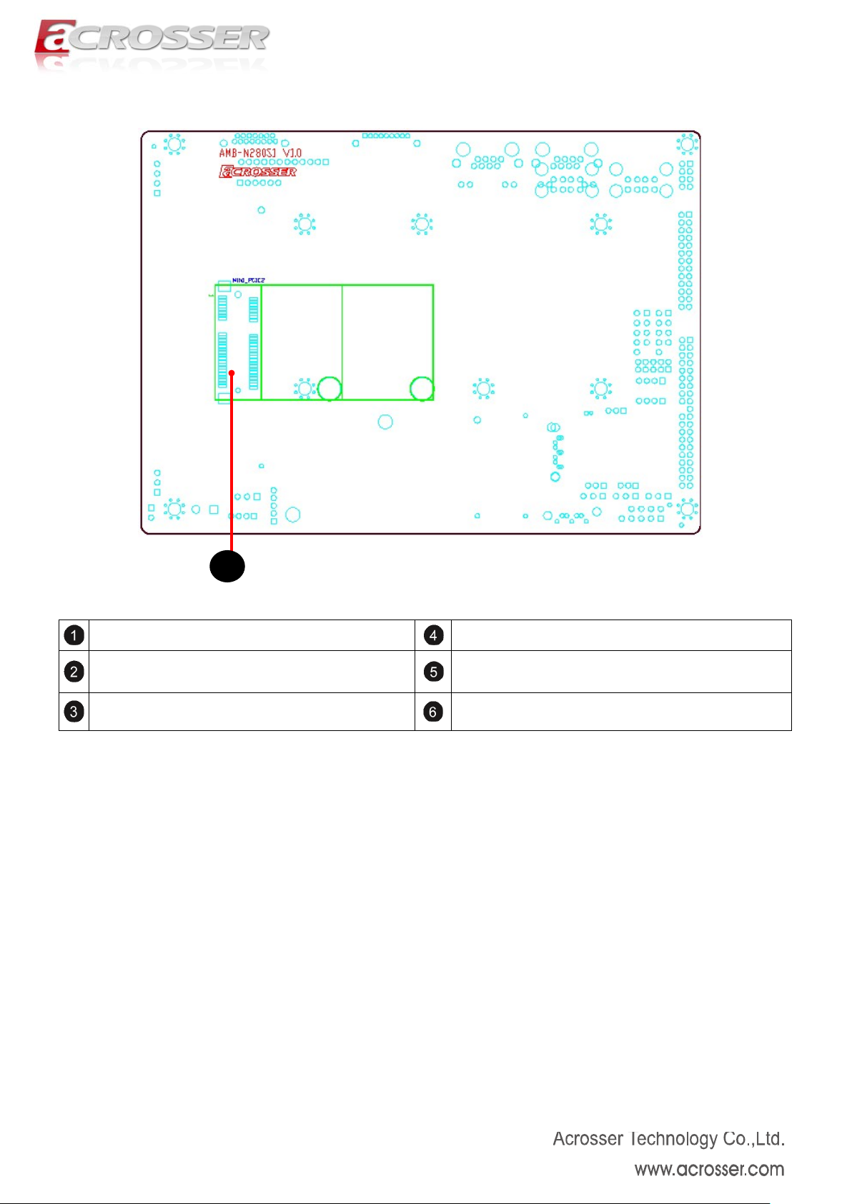
7
Mini PCI-E1*
Mini-PCIe Socket
Mini PCI-E2*
6
Bottom Side
Intel N2800 CPU 1.86GHz
DIMM 1
204-Pin DDR3 Socket
SIM Card slot
* The Mini-PCIE1 supports 3G module but cannot supports mSATA module.
And Mini-PCIe2 supports mSATA module only.
Intel NM10 PCH
Mini-PCIe Socket
Page 8

8
ATX1
Pin Header for System Fan2
Pin Header for SATA Power
F_PANEL1
SW
Pin Header for COM5, RX/TX only
SATA1
Pin Header for LPT
1
16 5 7
11
18
6
10
13 2 14 3 12 9 8 174
15
19 2120
22
22
2.2 Location & Definition of Jumpers and Headers
Power Input Header
JCMOS1
Pin Header for CMOS
Pin Header for front panel LED and
J_VGA1 (Reserved)
Pin Header for DB15 VGA connector
J_AUDIO1
Pin Header for front SPK and MIC
J_GPIO1
Pin Header for GPIO
LPT1
LVDS_P1
Pin Header for LVDS backlight
LVDS1
Pin Header for LVDS
SATA_P1
J_COM1-4
Pin Header for 4 Serial ports
J_COM5
J_COM6
Pin Header for COM6, RX/TX only
JP3 & JP4
For RS-232, RS-485 function
selection of COM6
J485_1
Pin Header for RS485 signal
SYS_FAN1
Pin Header for System Fan1
SYS_FAN2
F_USB1
Pin Header for front USB port
J_KBMS1
Pin Header for PS/2 KB and MS
SATA Port1
ATX2 (Reserved)
Power output Header
JSATA1 (Reserved)
SATA DOM Power output Header
Page 9
9
[1] Power Input Header(4*1 Pin 2.54mm)
Pin Definition Pin Definition
ATX1
1
3
+12V IN
GND
2
4
+12V IN
GND
* Please use the DC Power Cable in accessory to avoid the System damage.
[2] CMOS Control Jumper (3*1 Pin 2.54mm)
Setting Function
JCMOS1
1-2 Normal (Default)
2-3 Clear CMOS
[3] Front Panel Header(5*2 Pin 2.54mm)
Pin Definition Pin Definition
1 HD LED+ 2 Power LED+
3 HD LED- 4 Power LED5 GND 6 PW+
F_PANEL1
7 RESET 8 PW9 N/C
[4] KBMS Header (6*1 Pin 2.0mm)
J_KBMS1
Pin Definition Pin Definition
1
3
5
KB_CK1
MS_CK1
+5V
[5] F_AUDIO Header(4*2 Pin 2.54mm)
Pin Definition Pin Definition
1 OUT_R 2 MIC_R
3 GND 4 GND
5 GND 6 GND
J_AUDIO1
7 OUT_L 8 MIC_L
2
4
6
KB_DT1
GND
MS_DT1
Page 10

10
Pin
Definition
Pin
Definition
[6] GPIO Header(5*2 Pin 2.00mm)
Pin Definition Pin Definition
1
3
J_GPIO1
5
7
9
GPIO39(0x504 Bit7)
[7] LPT Header (13*2 Pin 2.0mm)
Pin Definition Pin Definition
1
3
5
7
9
11
GPIO6 (0500 Bit6)
GPIO15 (0501 Bit7)
GND
GPIO33(0504 Bit1)
LPT1
LPT2
LPT3
LPT4
LPT5
LPT6
2
4
6
8
10
12
2
4
6
8
10
GPIO22(0502 Bit6)
GPIO38(0x504 Bit6)
GPIO7(0500 Bit7)
GPIO36(0x504 Bit4)
+5V
LPT14
-ERR
LPT16
LPT17
GND
GND
13
15
17
LPT1
19
21
23
25
LPT7
LPT8
LPT9
-ACK
BUSY
PE
SLCT
14
16
18
20
22
24
26 GND
[8] LVDS Back Light Control Header(5*1 Pin 2.0 mm)
1
+12V
LVDS_P1
* LVDS_P1 is not support Brightness control
3
5
LVDS_ENABKL
+5V
2
4
GND
GND
GND
GND
GND
GND
GND
N/C
Page 11

11
[9] LVDS Header(20*2 Pin 1.25mm)
LVDS1
Pin Definition Pin Definition
1 VDD_PANEL 2 VDD_PANEL
3 GND 4 GND
5 VDD_PANEL 6 VDD_PANEL
7 LVDS_A_DATA0- 8
9 LVDS_A_DATA0+ 10
11 GND 12
13 LVDS_A_DATA1- 14 N/A
15 LVDS_A_DATA1+ 16 N/A
17 GND 18 GND
19 LVDS_A_DATA2- 20 N/A
21 LVDS_A_DATA2+ 22 N/A
23 GND 24 GND
25 LVDS_A_CLK- 26 N/A
N/A
N/A
GND
27 LVDS_A_CLK+ 28 N/A
29 GND 30 GND
31 LDDC_DATA 32 LDDC_CLK
33 GND 34 GND
35 N/A 36 N/A
37 N/A 38 N/A
39 NC 40 GND
*Attention: The output default value of VDD_PANEL is 3.3V,it also can be 5V or 12V by changing
the hardware!
[10]SATA Power Supply Header (4*1 Pin 2.00mm)
Pin Definition Pin Definition
SATA_P1
1
3
+12V
GND
2
4
GND
+5V
Page 12

12
[11] Serial Port 1-4 Header(20*2 Pin 2.0 mm)
Pin Definition Pin Definition
1
3
DCD
TXD
[2]
2
4
RXD
DTR
5
7
9
11
13
15
17
19
21
23
25
GND
RTS
RI
DCD
TXD
GND
RTS
[3]
RI
DCD
TXD
GND
[2]
[2]
6
8
10
12
14
16
18
20
22
24
26
DSR
CTS
GND
RXD
DTR
DSR
CTS
N/A
RXD
DTR
DSR
RTS
[3]
RI
NC
TXD
GND
RTS
NC
[4]
[4]
J_COM1-4
27
29
31
33
35
37
39
[12] Serial Port 5 Header(3*1 Pin 2.54mm)
J_COM5
Pin Definition Pin Definition
1 RXD 2 TXD
3 GND
[13] Serial Port 6 Header(3*1 Pin 2.54mm)
Pin Definition Pin Definition
28
30
32
34
36
38
40
CTS
GND
RXD
DTR
DSR
CTS
GND
J_COM6
1 RXD 2 TXD
3 GND
*Workable in RS-232 mode only
Page 13

13
J485_1
[14] Serial Port 6 Working Mode selection Header(two 3*1 Pin 2.54mm)
Header Settings Working Mode
JP3 1-2
JP3、JP4
JP4 1-2
JP3 2-3
JP4 2-3
[15] RS485 Header(2*1 Pin 2.54mm)
Pin Definition Pin Definition
1 RS485+ 2 RS485-
*Workable in RS-485 mode only
[16] System Fan1 Header (3*1 Pin 2.54 mm)
Pin Definition Pin Definition
SYS_FAN1
1 GND 2 + 12V
3 FANIO1
RS-485
RS-232(Default)
[17] System Fan2 Header (3*1 Pin 2.54 mm)
Pin Definition Pin Definition
SYS_FAN2
1 GND 2 + 12V
3 FANIO2
[18] USB Header(5*2 Pin 2.54 mm)
Pin Definition Pin Definition
1 + 5 V 2 + 5 V
3 USBP4- 4 USBP5-
F_USB1
5 USBP4+ 6 USBP57 GND 8 GND
10 N/C
* It cannot use USB Hub with power adaptor that connects to USB port.
Page 14

14
[19] VGA Header(12*1 Pin 2.00 mm)
Pin Definition Pin Definition
1 CRT_ON 2 VSYNC
3 HSYNC 4 GND
5 RED 6 GND
7 GREEN 8 GND
J_VGA1
9 BLUE 10 GND
11 DDCDAT 12 DDCCLK
[21] ATX2 Power Output Header (4*1 Pin 2.54mm)
Pin Definition Pin Definition
+12V
GND
2
4
ATX2
1
3
[22] SATA DOM Power Output Control Jumper (3*1 Pin 2.54mm)
GND
+5V
Setting Function
JSATA1
[1] The Mini-PCIe1 supports 3G module but cannot supports mSATA module.
And Mini-PCIe2 supports mSATA module only.
[2]The output default value (Pin 1 of COM1,COM3) is DCD and also can be 5V or 12V by changing the
hardware.
[3] The output default value (Pin 9 of COM3) is RI and also can be 5V or 12V by changing the hardware.
[4] The output default value (Pin 1 and Pin 9 of COM3,COM4) is NC, and also can be 5V or 12V by
changing the hardware.
1-2 Pin 7 Output: GND (Default)
2-3 Pin 7 Output: +5V
[5] It cannot use USB Hub with power adaptor that connects to all USB port.
Page 15

15
Chapter 3 B IOS Settings
This chapter describes the BIOS menu displays and explains how to perform common tasks
needed to get the sys tem u p and r u nni ng . I t al so gives detailed expl anati o n o f th e el e men t s found
in each of the BIOS menus. The following topics are covered:
Main Setup
Advanced Setup
Chipset Setup
Boot Setup
Security Setup
Save & Exit
Page 16

16
3.1. Main Setup
Once you enter the AMI BIOS™ CMOS Setup Utility, the Main Menu will appear on the screen.
Use the arrow keys to highlight the item and then use the <Pg Up> <Pg Dn> keys to select the
value you want in each item.
Note: Listed at the bottom o f the menu ar e th e con tr ol keys. If you need any help with the item
fields, you can press the <F1> key, and it will display the relevant information.
Option Choice Description
BIOS Information
BIOS Vendor
Core Version
Compliancy
N/A This item displays the BIOS Information
N/A This item displays the BIOS vendor
NA This item displays the Core Version
N/A This item displays the BIOS Compliancy
Page 17

17
Project Version
Motherboard Version
Built Data & Time
System Date
System Time
Access Level
N/A This item displays the Project Information.
N/A This item displays the Mother Board Model.
N/A This item displays the Built information
N/A Set the date. Use Tab to switch between Date elements
N/A Set the time. Use Tab to switch between Date elements
N/A Set the system access level.
Page 18

18
3.2. Advanced Setup
Option Choice Description
ACPI Settings
Power On
CPU Configuration
IDE Configuration
USB Configuration
SMART Settings
Super IO
N/A ACPI Options Settings
N/A Power Fail settings
NA This item displays the CPU and Parameters.
N/A SATA and IDE port configuration.
NA Monitor hardware status
NA Power Sub System
NA System Super IO Chip Parameters.
HW Monitor
NA This item displays the H W Monitor Parameters
Page 19

19
3.2.1 ACPI Settings
Option Choice Description
Enable ACPI Auto
Configuration
Enable Hibernation
ACPI Sleep State
Enabled / Disabled Enable or disable APCI Settings
Enabled / Disabled Enable or disable Hibernation
Disable / S1 Only /
Define ACPI State whil e Su spend button pressed
S3 Only
Page 20

20
3.2.2 Power On Configuration
Option Choice Description
PowerOn After
Power Fail
Power On/ Power
Define the system Power status after Power Fail.
Off / Last Status
Page 21

21
3.2.3 CPU Configuration
Option Choice Description
Hyper-Threading
Execute Disable Bit
Enabled / Disabled Enabled or Disabled the Hyper-Threading Technology.
Enabled / Disabled Enabled or Disabled the Execute Disable Bit Function
Page 22

22
3.2.4 IDE Configuration
Option Choice Description
SATA Co ntroller(s)
SATA Mode
Selection
SATA Port 0
SATA Port 0 Hot Plu g
SATA Port 1
SATA Port 1 Hot Plu g
Enabled / Disabled Enable or Disable SATA Device.
IDE / AHCI Determines how SATA controller(s) operate.
Enabled / Disabled Enable or Disable SATA Port
Enabled / Disabled Designates this port as hot Pluggable
Enabled / Disabled Enable or Disable SATA Port
Enabled / Disabled Designates this port as hot Pluggable
Page 23

23
3.2.5 USB Configuration
Option Choice Description
Legacy USB
Support
EHCI Hand-Off
Enabled / Disabled
Enabled / Disabled
Enables Legacy USB support. AUTO option disables legacy
support if no USB devices are connected. DISABLE option
will keep USB devices available only for EFI applications.
Enable or Disable the EHCI Hand-Off Function. It Could
Disable if driver of OS is not supported.
Page 24

24
3.2.6 SAMRT Configuration
Option Choice Description
SMART Self Test
Enabled / Disabled Enable or Disable the SMART Self Test
Page 25

25
3.2.7 Super IO Configuration
Option Choice Description
COM1
COM2
COM3
COM4
COM5
COM6
LPT
NA Set Parameters of COM1 Port
NA Set Parameters of COM2 Port
NA Set Parameters of COM3 Port
NA Set Parameters of COM4 Port
NA Set Parameters of COM5 Port
NA Set Parameters of COM6 Port
NA Set Parameters of LPT Port
Page 26

26
3.2.7.1 COM Port Configuration
COM Port 1~6 Configurations
Option Choice Description
Serial Port
Device Settings
Enabled / Disabled Enable or Disable this Serial Port (1~6)
NA Show the Parameters of Serial Port (1~6)
Page 27

27
3.2.7.2 LPT Port Configuration
Option Choice Description
Parallel Port
Device Settings
Device Mode
Enabled / Disabled Enable or Disable this Parallel Port
NA Show the Parameters of Parallel Port
STD / SPP / EPP /
Change the Printer Port Mode
ECP
Page 28

28
3.2.8 HW Monitor
Page 29

29
3.3. Chipset Setup
Option Choice Description
HOST Bridge
South Bridge
NA HOST Bridge Options and Settings
NA Sout h Bridg e Options and Settings
Page 30

30
3.3.1 HOST Bridge
Option Choice Description
Intel IGD
Configuration
Memory Information
NA Intel IGD Options and Settings
NA Display the memory Information
Page 31

31
3.3.1.1 Intel IGD Configuration
Option Choice Description
IGFX – Boot Type
LCD Panel Type
Panel Scaling
Active LVDS
Fixed Graphic
Memory Size
VGA /LVDS / HDMI HOST Bridge Options and Settings
VBIOS Default/LCD Select Panel Type Used
Auto / Force / Off /
Select LCD Panel Scaling Options used
Maintain
Disable / Internal /
Select Active LVDS Configuration
eDP
128MB / 256MB Fixed Graphic Memory Size Selection
Page 32

32
3.3.2 South Bridge
TPT Devices
Option Choice Description
NA Enable /Disable Intel IO Controller Hub devices
Page 33

33
3.3.2.1 TPT Device
Option Choice Description
Azalia Controller
Select USB Mode
USB Functions
USB 2.0(EHCI)
Support
SMBus Controller
Disable / HD Audio Enable or Disable the Azalia Audio Controller
By Ports / By
By Port or By Controller to setting the USB Mode
Controller
X USB Ports Enable or Disable the USB Ports (x : 0~8)
Enable / Disable Enable or Disable the USB EHCI
Enable / Disable Enable or Disable the SMBus
Page 34

34
3.4. Boot Setup
Option Choice Description
Bootup Number
Lock
Fullscreen Logo
CSM Parameters
On / Off Enable or Disable the Azalia Audio Controller
Enable / Disable By Port or By Controller to setting the USB Mode
NA Enable or Disable the USB Ports (x : 0~8)
Page 35

35
3.4.1 CSM Parameters
Option Choice Description
Launch PXE OpROM
Policy
Launch Storage
OpROM Policy
Launch Video
OpROM Policy
Launch PCI device
ROM Policy
Do not Launch /
Controls the execution of UEFI and Legacy PXE OpROM
UEFI / Legacy
Do not Launch /
Controls the execution of UEFI and Legacy Storage OpROM
UEFI / Legacy
Do not Launch /
Controls the execution of UEFI and Legacy Video OpROM
UEFI / Legacy
Do not Launch /
Controls the execution of UEFI and Legacy PCI device ROM
UEFI / Legacy
Page 36

36
3.5. Security setup
Option Choice Description
Administrator
Password
User Password
NA Set Administrator Password
NA Set User Password
Page 37

37
3.6. Save & Exit Setup
Option Choice Description
Save Changes and
Exit
Discard Changes
and Exit
Save Changes
Discard Changes
Restore Defaults
Save as User
Default
Restore User
Defaults
Yes / No Reset System after Save the Changes
Yes / No Reset System but not Saving the Changes
Yes / No Saving the changes done so far
Yes / No Discard the changes done so far
Yes / No Restore/Load Default value for all the setup options
Yes / No Save the changes done so far as User Default
Yes / No Restore/Load User Default value to all the setup options
Page 38

38
Chapter 4 Function Descr iption
4.1. DC Power input connection
AMB-N280S1 needs DC 12V to power the board.
* Please use the DC Power Cable in accessory to avoid the System damage.
4.2. Digital Inputs
There are 4 D igital Inputs you could u se for many applications.
4.3. Digital Outputs
There are 4 D igital Outputs you could use for many applications.
4.4. RS-232 Ports
The COM1/COM2/COM3/COM4/COM5/COM6 are connected throug h a cable(pin
header). Users need to plug into RS-232 or RS-485 connector. For RS-485, please refer to
JP3, JP4 setting in pa ge 12 of Use r Ma nual.
4.5. Serial ATA (SATA)
There is one SATA port on the AMB-N280S1. There is also one SATA power connectors
for the SATA hard disks and it has 1pcs S ATA power cable in Accessory . I f you need more
SATA power cable, please contact your Acrosser sales representative for the quotation
4.6. USB
There are four USB 2.0 interfaces on the AMB-N280S1. Two USB connectors are located
on the edge of the board. One 2X 5 pin in te r na l con nec tor s up p or ts the o the r two US B por t s.
You need a spe cial cable for using the se two USB ports and they are optional accessories.
 Loading...