

Page 1

Revision: 1.0
ACE-Mini
System Guide
Revision Description Date
1.0 Release 2009/12/29
1
Page 2

Revision: 1.0
Content s
1 Introduction to ACE-MINI .........................................................4
1.1 Specifications.................................................................................... 8
1.2 Packing List....................................................................................... 8
1.3 System Dissection............................................................................ 9
2 Procedures of Assembly/Disassembly ...................................12
2.1 Installing the power cable hook .................................................... 12
2.2 Installing the 2.5” Hard Disk Driver (HDD).................................... 15
2.3 Installing the mainboard procedures............................................ 22
2.4 Installing the ACE-B2019/A Batteries............................................ 24
3 ACE-B2019/A Series Guide (ACE-B2019, ACE-B2019A)........27
3.1 Block Diagram................................................................................. 27
3.2 ACE-B2019/A H/W Information ...................................................... 28
3.2.1 ACE-B2019/A LAYOUT (Top side)...........................................................28
3.2.2 ACE-B2019/A LAYOUT (Bottom side).....................................................29
3.3 Connectors and Jumpers Setting ................................................. 30
3.3.1 Locations...................................................................................................30
3.3.2 Components and Jumps Setting List......................................................31
3.4 AGC Register Description.............................................................. 36
3.4.1 PCI Configuration Register......................................................................36
3.4.2 SRAM Memory Address Map...................................................................42
3.4.3 I/O-Interface Address Map .......................................................................43
3.6 OXUPCI954 Drive Installation Guide............................................. 79
3.7 Electrical Characteristics............................................................... 88
3.7.1 Basic Electrical Characteristics ..............................................................88
3.7.2 72-PIN Golden Finger...............................................................................89
3.7.3 Spare GPIO connector (For ACE-B2019A Only).....................................91
3.7.4 AGC Port Assignment ..............................................................................93
3.7.5 NOTES (72-PIN Gold Finger I/O)..............................................................97
2
Page 3

Revision: 1.0
4 Acrosser Intelligent Reel Controller (AR-B2009)....................99
4.1 Structure of Acrosser Intelligent Reel Controller ...................... 100
4.2 AR-B2009 LA YOUT........................................................................ 101
4.3 CONNECTOR S SETTING............................................................. 102
4.4 REEL Control Step........................................................................ 107
3
Page 4
Revision: 1.0
1 Introduction to ACE-MINI
ACE-MINI series is a solution for gaming machine system integrators who want to use
low cost and flexible MINI-ITX motherboard as the computing platform. ACE-MINI contains a
PCI bus gaming I/O control card (ACE-B2019/A), an AC input power supply and a chassis.
Any MINI-ITX motherboard with a PCI slot can fit in the ACE-MINI. There are five
configurations in ACE-MINI series.
Table 1 ACE-MINI SKU table
Configuration Chassis Gaming I/O
card
ACE-MINI Yes ACE-B2019 No No 180W
ACE-MINI-A Yes ACE-B2019A No No 180W
ACE-MINI5495 Yes ACE-B2019 AR-B5495 No 100W
ACE-MINI5495A Yes ACE-B2019A AR-B5495 No 100W
ACE-MINI5495R Yes ACE-B2019A AR-B5495 Yes 100W
Note: There will be more standard MINI-ITX mother board from Acrosser. Please contact
with Acrosser’s sales representative for further information.
Table 2 Comparison of ACE-B2019 and ACE-B2019A
Features AR-B2019 AR-B2019A
Serial Ports No 1. COM1: TTL/RS232.
Intrusion logger No Yes
SRAM 256KB 512KB x 2
Secured real time clock No Yes
iButton retainer, ProtectU No Yes
GPIO No 28 bits
Battery low detection No Yes
Mother
board
Reel mechanism
controller
(AR-B2009)
2. COM2:
RS232-COM2/ccTlak1
3. COM3:
RS232-COM3/ccTlak2
PSU
4
Page 5
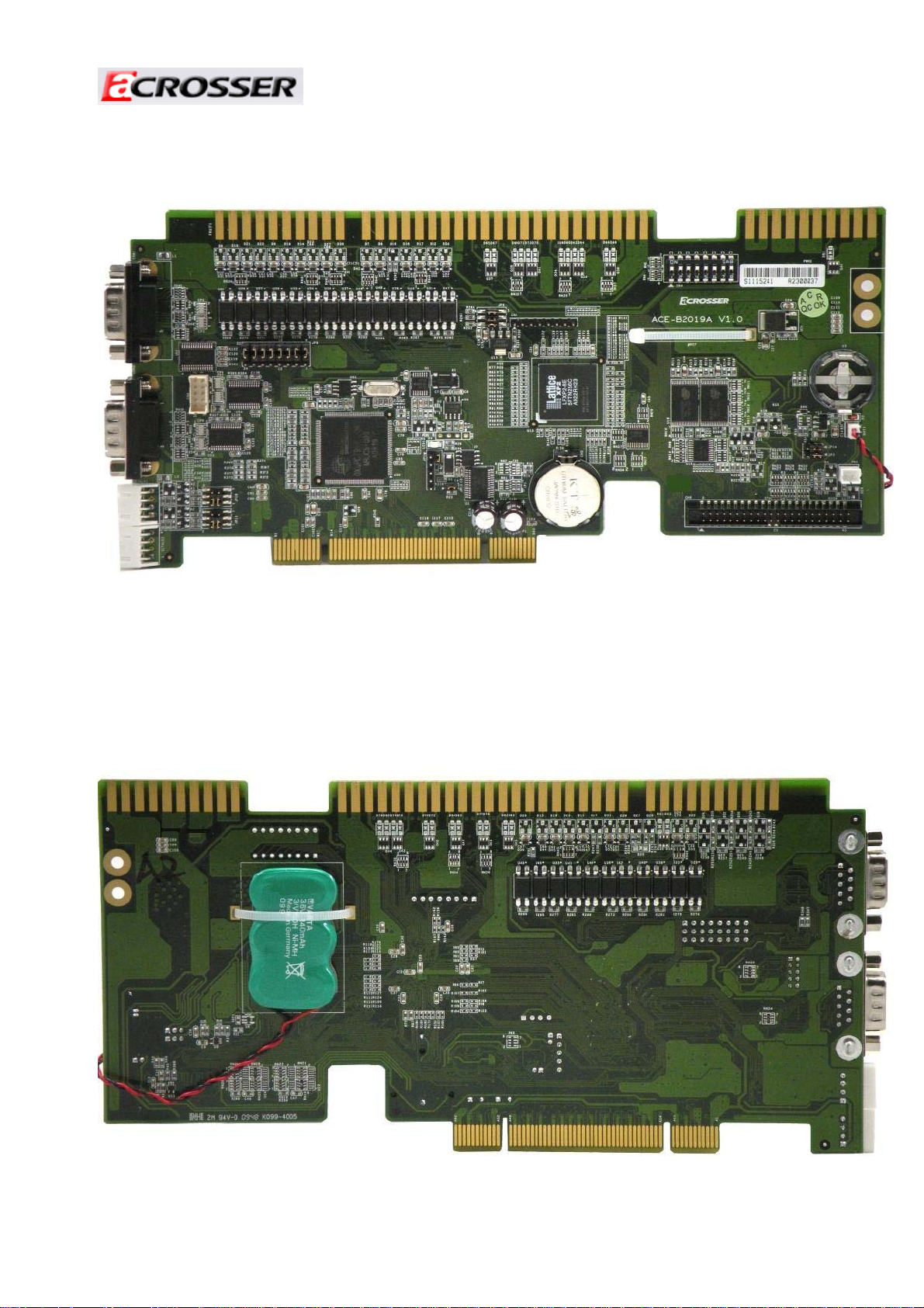
ACE-B2019A Component-side:
Revision: 1.0
ACE-B2019A Bottom-side:
5
Page 6
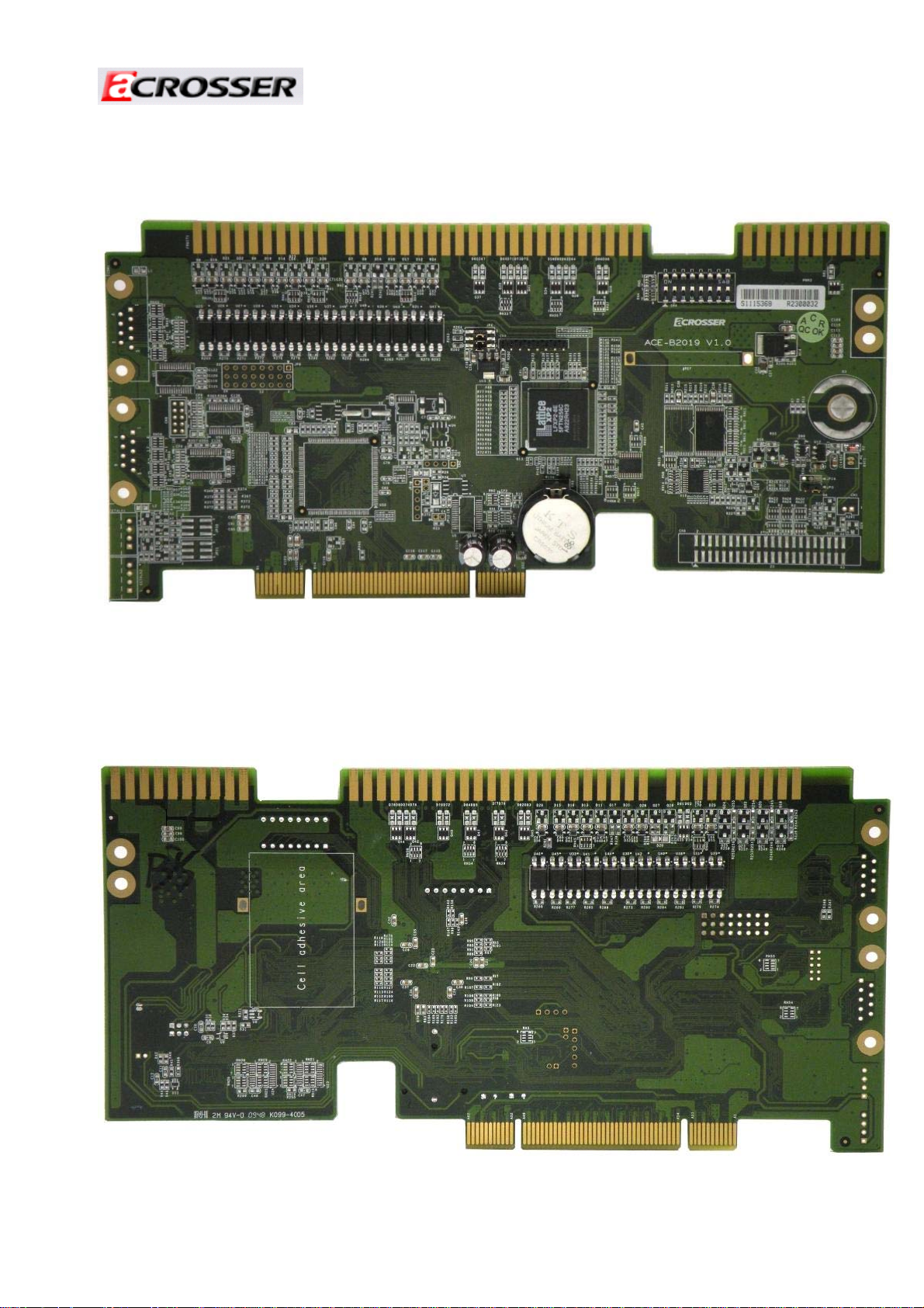
ACE-B2019 Component -side:
Revision: 1.0
ACE-B2019 Bottom-side:
6
Page 7

Revision: 1.0
Features:
Mini-ITX chassis with PCI Gaming I/O card.
Is suitable for any Mini-ITX motherboard with PCI slot.
Standard 8-liner 72-pin plus 10-pin interface.
30 Digital Inputs, 27 digital outputs, 512KB NVRAM , 4 x 16-bittimers.
Chassis intrusion switch.
3 x Serial ports, Intrusion logger, Real Time Clock, Software protection (AR-B2019A).
Description Mini ITX Chassis with Gaming Control Card
Dimension Depth: 266.2 * 245.5 * 134.5mm.
System Thermal One system fan.
CPU Board Standard Mini-ITX motherboard with PCI slot.
Storage One 2.5” HDD bay.
Chassis Intrusion
Switch
Front Panel 1. Standard Mini-ITX bracket opening.
Gaming I/O 1. 8-liner interface.
Software
development kit
Power Supply 180 or 100 Watts ATX power supply.
One chassis intrusion switch.
2. 1 x PCI card bracket.
3. D-sub 9 connector opening.
4. Power LED.
5. ATX power switch.
2. 30 x 5KV optical isolated digital inputs.
3. 24 x 500mA MOSFET outputs.
4. 2 x 1000mA output for tower lamps.
5. One 180 degrees 8-bit readable DIP switch.
6. Four 16-bit timers with timeout interrupt.
7. 256KB or dual 512KB SRAM with battery backup.
8. Optional advanced version (AR-B2019A).
a. 3 serial ports (RS-232C, TTL, ccTalk). SAS bit-9 protocol support.
b. Intrusion logger.
c. Secured real time clock.
d. Software security: ProtectU(programmable ID) & Dallas iButton
socket.
e. Reel mechanism controller, support up to 6 reels
(ACE-MINI5495R).
1. Supports Windows XP, XP embedded and Linux.
2. Device drivers.
3. Application Program Interface (API).
7
Page 8
1.1 Specifications
Item Description
System ACE-MINI Series
CPU Board AR-B5495(ACE-MINI5495(A)(R) model)
System Dimensions 265*254.5*134.5(mm)
1.2 Packing List
Description Quantity Remark
ACE-MINI series 1
AR-B5495 accessory pack 1
Mounting bracket
AC Power cord
CD ROM
SATA power cable
SATA cable
Revision: 1.0
ACE-MINI5495(A)(R)
model:
1. COM cable * 2
2. SATA power cable * 1
3. SATA cable * 2
4. IDE cable * 1
5. CD ROM
2
1
1
1 ACE-MINI(-A) model
1
8
Page 9
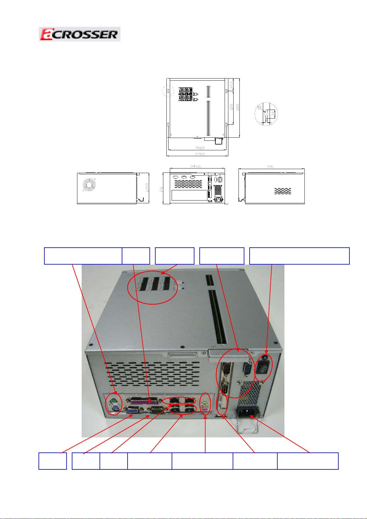
1.3 System Dissection
(1) Dimensions
Revision: 1.0
(2) Front Panel (ACE-MINI5495R model type)
Key board & mouse LPT1
Reel A~F COM 1~3
POWER SWITCH & LED
VGA
COM LAN USB 1~4
LINE IN/OUT
CC TALK
POWER JACK
9
Page 10
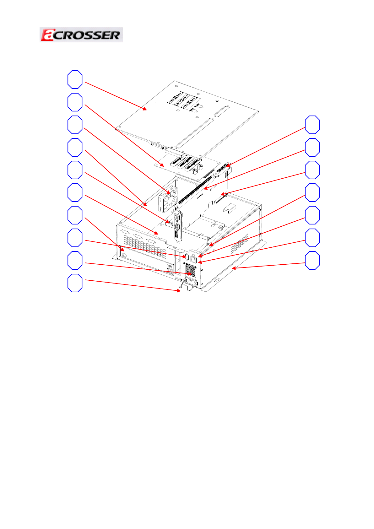
(3)System Configuration
1
2
Revision: 1.0
3
4
5
6
7
8
9
11
12
13
14
15
16
17
10
10
Page 11

Item Description Quantity
1 TOP COVER 1
2 AR-B2009(ACE-MINI5495R TYPE) 1
3 FAN 1
4 BOTTOM BASE 1
5 HDD BRACKET 1
6 AR-B5495(ACE-MINI5495(A)(R) TYPE) 1
7 MAIN BOARD IO BRACKET 1
8 COM3 1
9 POWER SUPPLY 1
Revision: 1.0
10 POWER CORD HOOK 1
11 SLOT 3.96mm 20PIN 1
12 SLOT 3.96mm 72PIN
1
13 ACE-B2019(A) 1
14 CHASSIS INTRUSION SWITCH 1
15 POWER LED 1
16 ATX POWER SWITCH 1
17 MOUNTING BRACKET 2
11
Page 12
Revision: 1.0
2 Procedures of Assembly/Disassembly
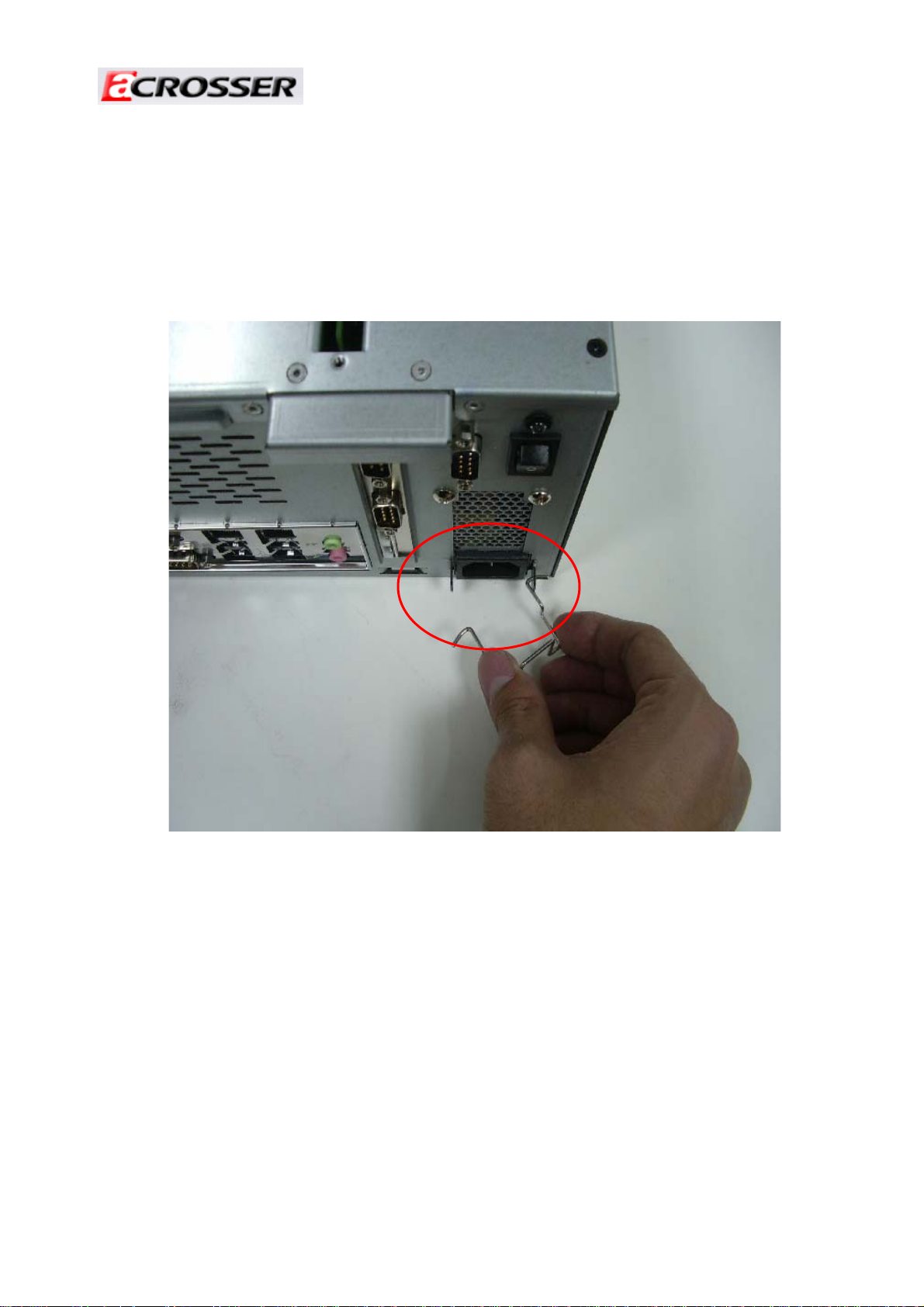
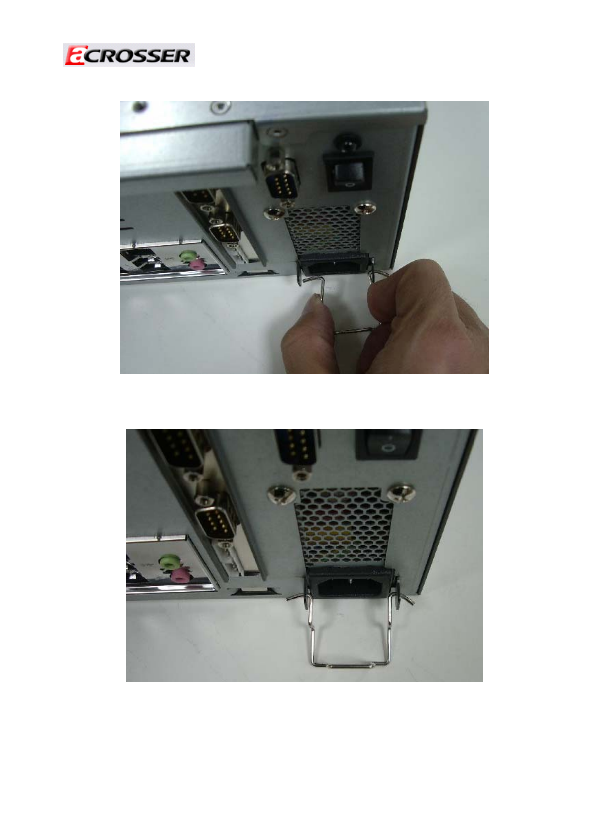
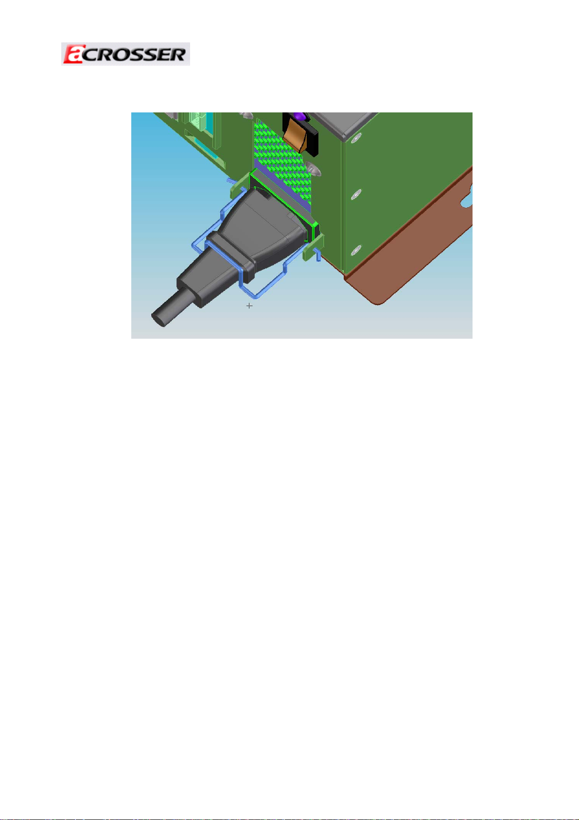
2.1 Installing the power cable hook
1. Please take out the hook that attached from packing package, and then install it on
position below.
2. The good way to install the hook, it should be installed the right side first then left side
installing.
12
Page 13
Revision: 1.0
3. Make sure the hook has been installed firmly.
13
Page 14
Revision: 1.0
14
Page 15
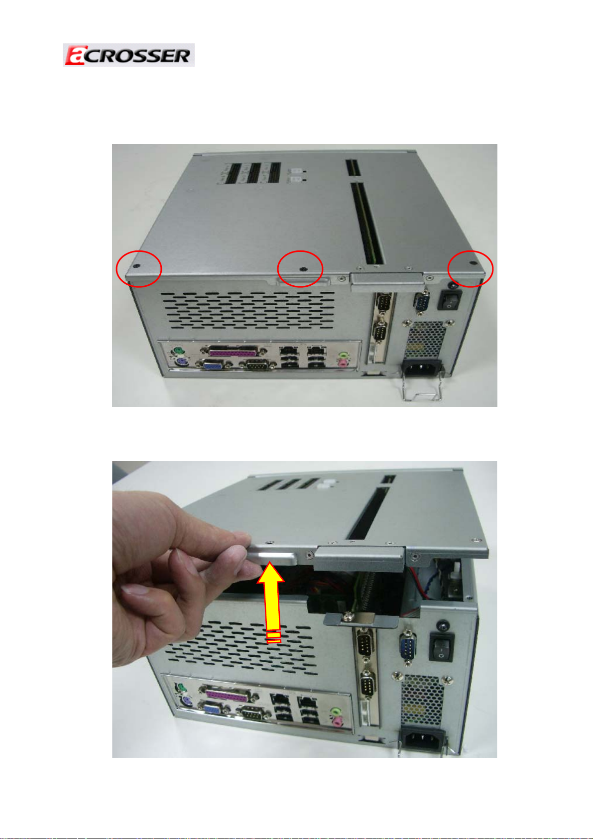
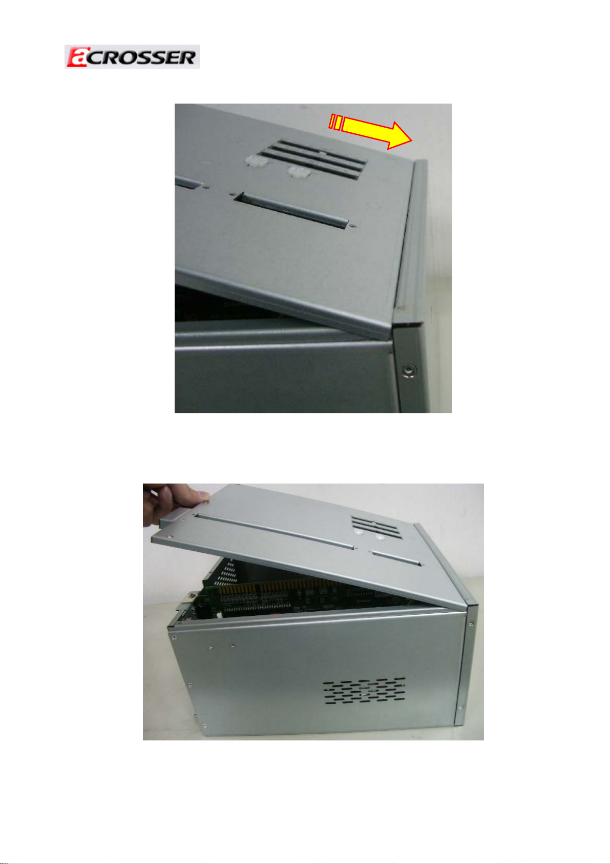
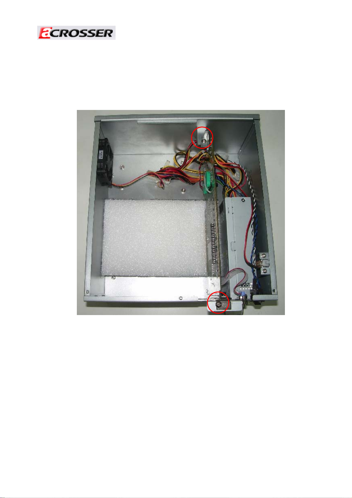
2.2 Installing the 2.5” Hard Disk Driver (HDD)
1. Unfasten three screws to take off the top cover.
Revision: 1.0
2. Open the top cover following the direction.
15
Page 16
Revision: 1.0
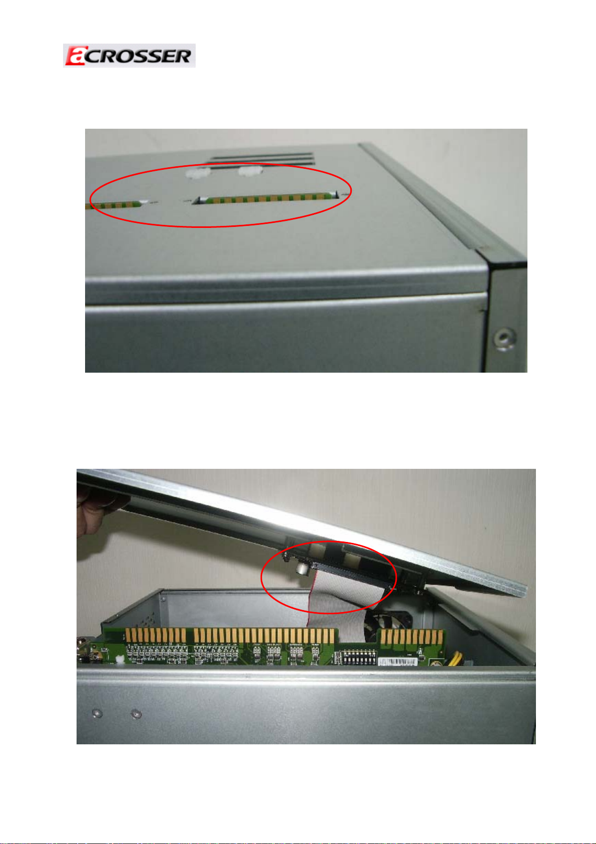
3. Before take off the top cover, please notice to keep away from the ACE-B2019 golden
finger.
4. If the system has a reel function (ACE-MINI5495R), please take care of the reel cable
connecting.
16
Page 17
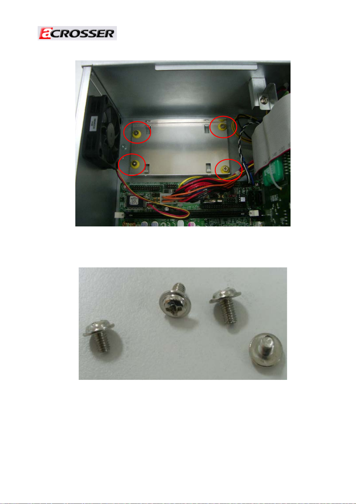
5. Release the HDD bracket via unscrewing four screws.
Revision: 1.0
6. Find the HDD screws (M3*5L) from packing packet.
17
Page 18
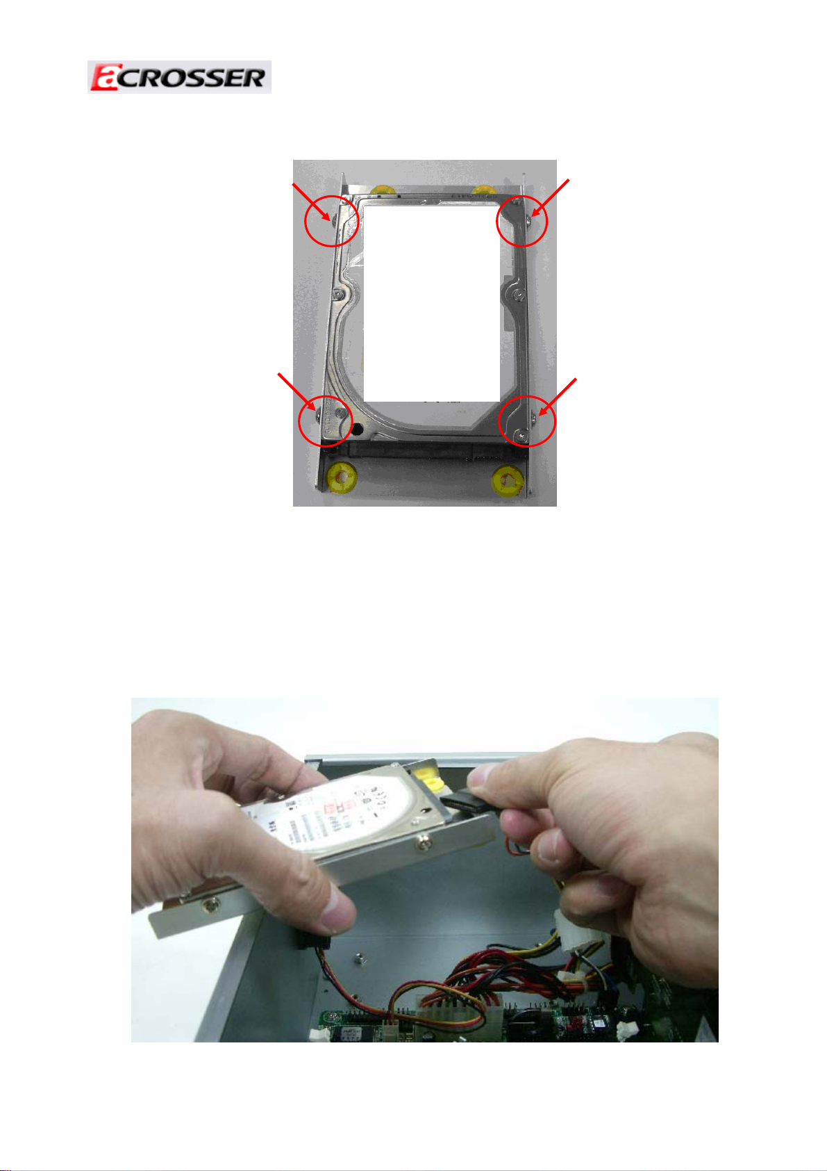
Revision: 1.0
7. Assemble the HDD in HDD bracket with four screws.(Notice the HDD direction)
8. Connect the SATA cable & power cable to the HDD.
(Notice: For ACE-MINI & ACE-MINI-A series, the power supply has no the SATA power
connector. Please take the SATA power adapter cable from packing packet. And then
connect to power supply first.)
18
Page 19
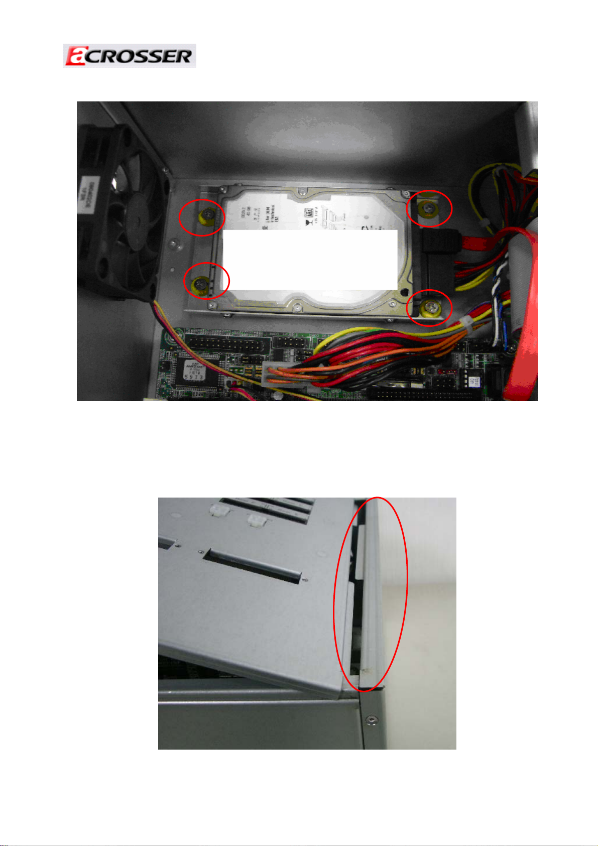
9. Fix the HDD module via four screws.
Revision: 1.0
10. Align the position to place the top cover back.
19
Page 20
11. Push the top cover into the bottom case following the direction below.
Revision: 1.0
12. Close the top cover.
20
Page 21
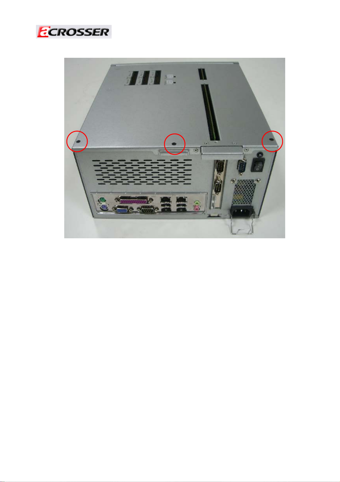
13. Fasten three screws to fix the top cover.
Revision: 1.0
21
Page 22
2.3 Installing the mainboard procedures
Only for ACE-MINI & ACE-MINI-A series.
1. Follow above steps to open the top cover.
2. Unfasten two screws to release ACE-B2019/A.
Revision: 1.0
22
Page 23
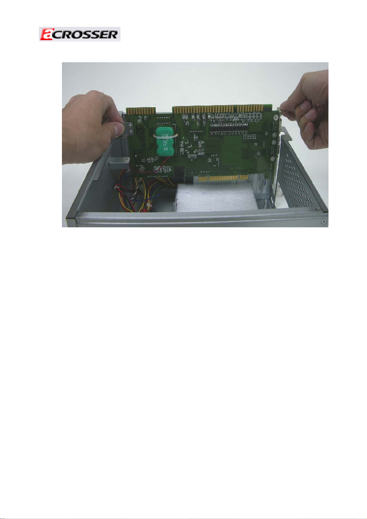
3. Take off the ACE-B2019(A) and remove the EPE.
Revision: 1.0
.
4. Follow the mainboard installation guide to install mainboard into ACE-MINI case.
5. Close the top cover.
23
Page 24
Revision: 1.0
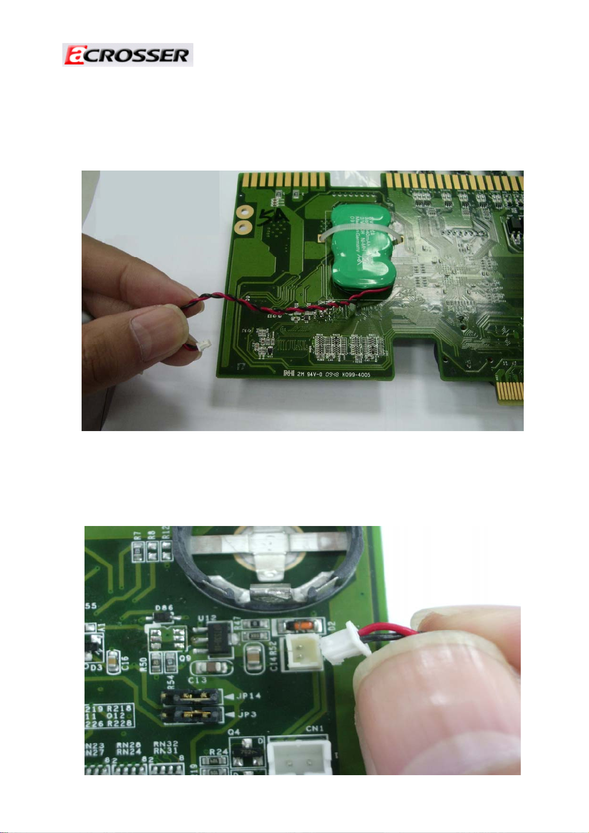
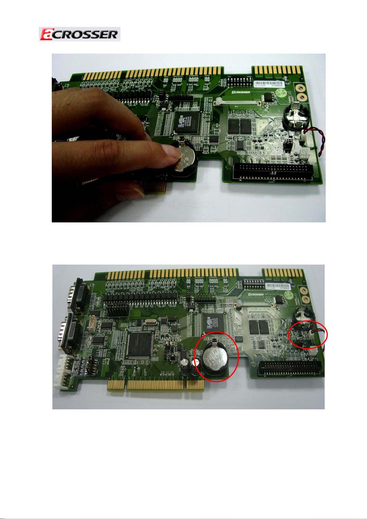
2.4 Installing the ACE-B2019/A Batteries
1. Please follow above steps to open the top cover of ACE-Mini and take out ACE-B2019/A .
2. Take rechargeable battery cable from the bottom side of ACE-B2019A .
(for ACE-B2019A only).
3. Plug rechargeable battery cable into BAT1 rechargeable battery connector (BAT1
connector is on the top side of ACE-B2019A).
(for ACE-B2019A only).
24
Page 25
Revision: 1.0
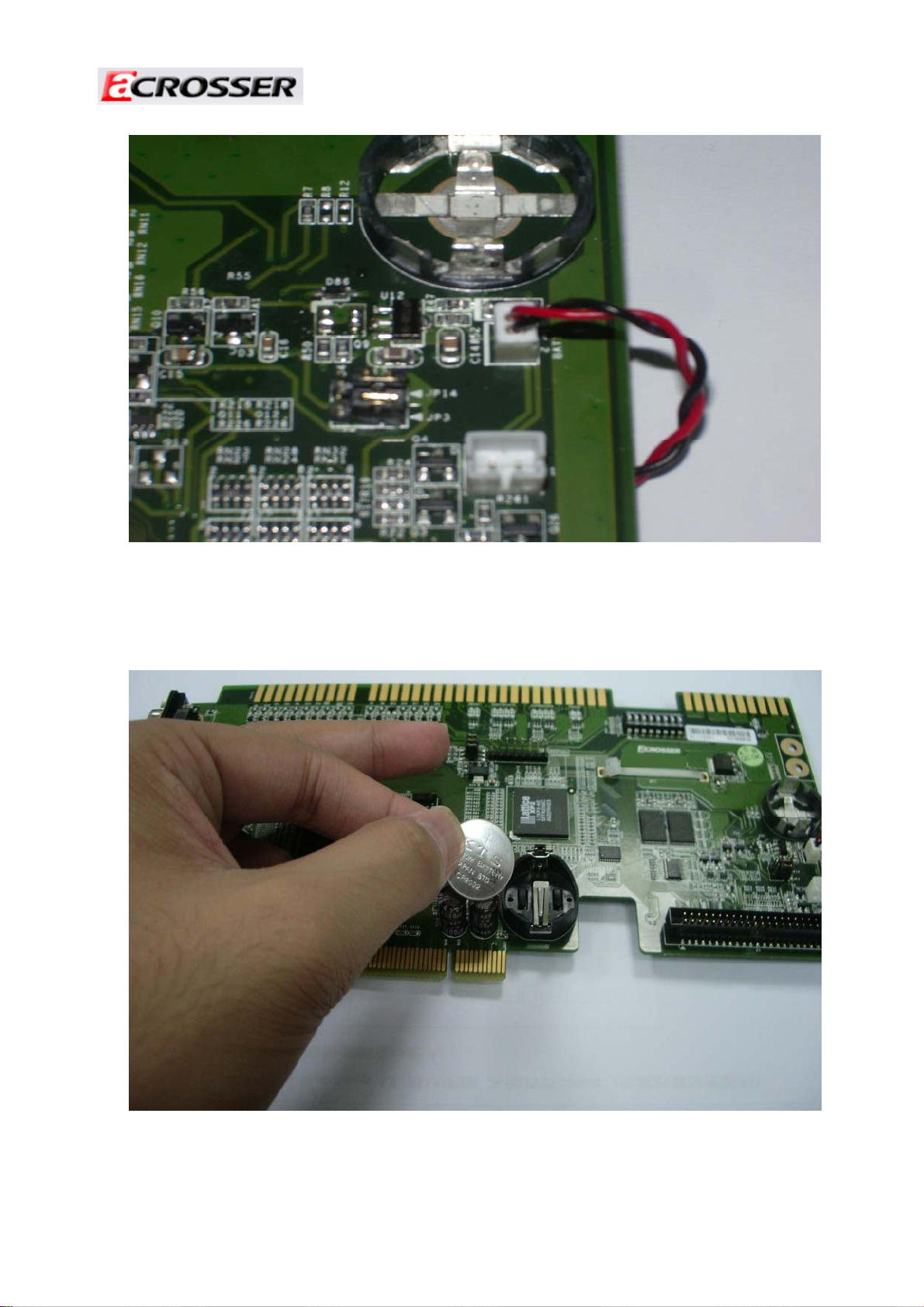
4. Please take out the CR2302 battery that attached from packing package, and then install
it into CN3 CR2032 Battery Holder (Place it upper side of the battery upward).
25
Page 26
Revision: 1.0
5. Final, the CR2032 and rechargeable batteries should be placed as below.
(ACE-B2019 only has CR2032 battery holder).
6. Install ACE-B2019/A into ACE-Mini and fasten two screws to place ACE-B2019/A, then
close top cover.
26
Page 27
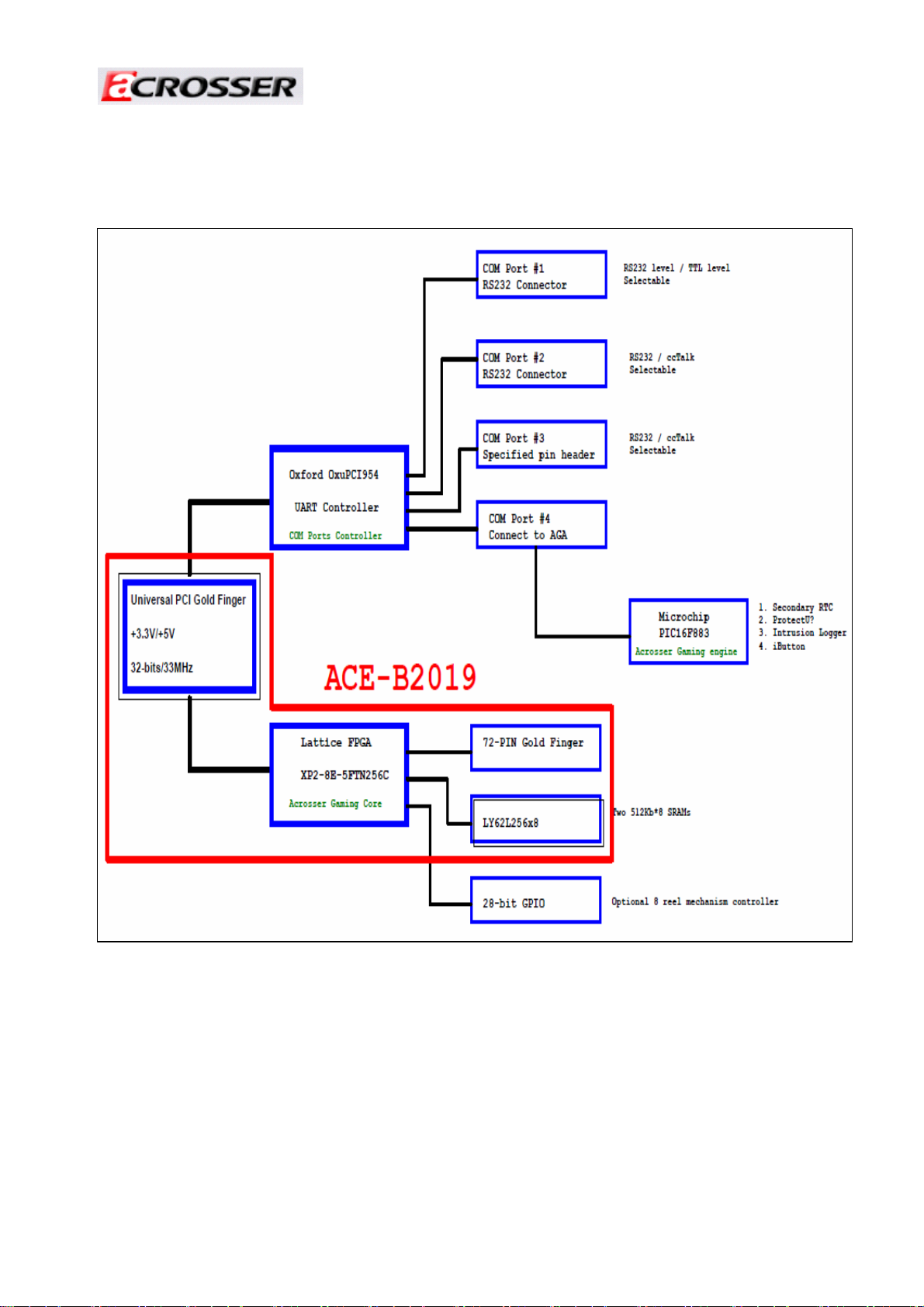
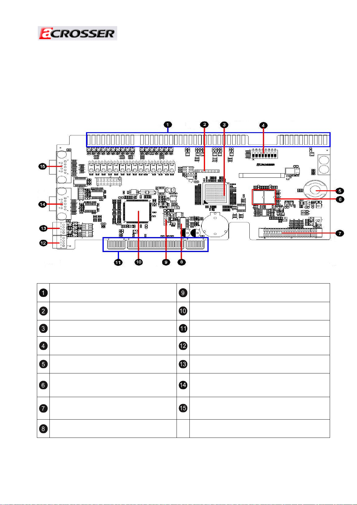
3 ACE-B2019/A Series Guide (ACE-B2019, ACE-B2019A)
3.1 Block Diagram
Revision: 1.0
Note:
☆ ACE-B2019 has only 256KB SRAM but AR-B2019A has two 512KB SRAMs.
27
Page 28
Revision: 1.0
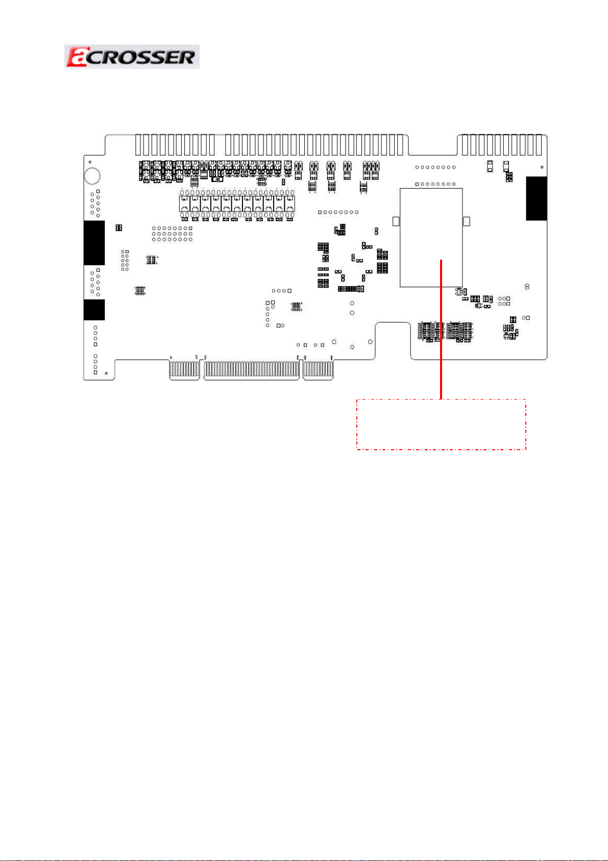
3.2 ACE-B2019/A H/W Information
This section describes the installation of ACE-B2019/A. At first, it shows the function
diagram and the layout of ACE-B2019(A). It then describes the unpacking information which
you should read carefully, as well as the jumper/switch settings for the ACE-B2019/A
configuration.
3.2.1 ACE-B2019/A LAYOUT (Top side)
FRUIT1
72-Pin Gold Finger & 20-Pin Gold Finger.
CN4
FPGA Programming Pin Header.
U13
AGC (Acrosser Gaming Core).
SW4
Intrusion Log Switch.
U3
i-Button Holder.
U17, U18
SRAM A. SRAM B.
(ACE-B2019 Only has 512KB SRAM A )
CN6
Reel Controller Connector (44pin mini-IDE Reel
Connector connects to AR-B2009).*
U5
AGA (Acrosser Gaming Engine).
*
*
Note:* for ACE-B2019A only.
JP1
AGA Programming Pin Header.
U50
OXuPCI954 UART Controller IC.
PCI
PCI Gold Finger.
ccTalk2
ccTalk Connector (Signal share with COM3).
ccTalk1
ccTalk Connector (Signal share with COM2).
COM2
RS232 Serial Ports COM2.
COM1
RS232 Serial Ports COM1.
*
*
*
*
*
*
28
Page 29
3.2.2 ACE-B2019/A LAYOUT (Bottom side)
Revision: 1.0
Rechargeable
Battery (ACE-B2019A Only)
29
Page 30
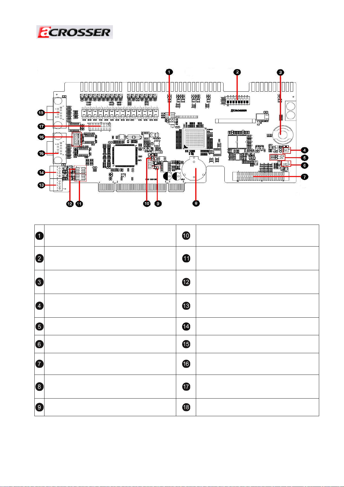
3.3 Connectors and Jumpers Setting
3.3.1 Locations
Revision: 1.0
JP6
Bill enable, Coin enable and Hopper sensor pre-set
header.
SW4
8-bit readable DIP switch.
U3
i-Button holder.
BAT1
BAT1 is rechargeable battery connector for AGA, RTC,
and SRAMB.
JP3, JP14
SRAM A, SRAM B clear pin header.
CN1
Case Intrusion Switch.
CN6
Reel Controller Connector (44pin mini-IDE Reel
Connector connects to AR-B2009).*
CN3
CR2032 Battery Holder.
JP13
Power on-off detect header.
*
*
*
*
Note:
1. * for ACE-B2019A only.
2. AR-B2009 functions please refer to chapter 4.
JP2
AGA power supply header.*
JP11
COM3 can be selected as RS232 serial port or
ccTalk2.
JP10
COM2 can be selected as RS232 serial port or
ccTalk1.
ccTalk2
ccTalk connector ( Signal share with COM3).
ccTalk1
ccTalk connector ( Signal share with COM2).
COM2
RS232 Serial Ports COM2.
CN8
RS232 Serial Ports COM3.
JP9
Selection of COM1 output voltage level is RS232C or
TTL.
COM1
RS232 Serial Ports COM1.
*
*
*
*
*
* (JST 2.0mm 2×5)
*
*
30
Page 31

3.3.2 Components and Jumps Setting List
1. JP6
Bill enable, Coin enable and Hopper
sensor pre-set header.
Connection State description
1-2
(BILL)
OPEN preset is “Low”
preset is “High”
CLOSE
(default)
3-4
(COIN)
OPEN preset is “Low”
CLOSE preset is “High”
(default)
5-6
(HOPPER)
OPEN preset is “Low”
CLOSE preset is “High”
(default)
3. U3*
i-Button holder.
Revision: 1.0
2. SW4
Intrusion log switch.
State descri.
ON GND (Low)
OFF +3.3V (High)
4. BAT1*
Rechargeable battery
connector.
Pin description
1 +4.2V
2 GND
31
Page 32

Revision: 1.0
5. JP3, JP14
SRAM A, SRAM B clear pin header
(ACE-B2019 has only 512KB SRAM A and
JP3)
Connection description
normal
1-2
(default)
2-3 short clear SRAM
6. CN1
Case Intrusion Switch Connector.
7. CN6*
Reel Controller Connector (44pin
mini-IDE Reel Connector connects to
AR-B2009).
Note: GPIO is standard CMOS 3.3V
Pin
1 MDAP 2 MDAN
3 MDBP 4 MDBA
5 GND 6 GND
7 Lamp_Inn 8 Lamp_Out
9 LAMP0 10 LAMP1
11 LAMP2 12 LAMP3
13 LAMP4 14 LED
15 LATCH_A 16 LATCH_B
17 GND 18 GND
19 LATCH_C 20 LATCH_D
21 LATCH_E( 22 LATCH_F
23 LATCH_G 24 LATCH_H
25 FB_A( 26 FB_B
27 +5V 28 +5V
29 FB_C 30 FB_D
31 FB_E 32 FB_F
33 +12V 34 +12V
35 FB_G 36 FB_H
37 +3.3V 38 +3.3V
39 GND 40 GND
41 GND 42 GND
43 LATCH_OE# 44 NC
Input/Output.
description
Pin
description
8. CN3
CR2302 Battery Holder.
32
Page 33

Revision: 1.0
9. JP13*
Power on-off detect header.
State description
enable
CLOSE
(default)
OPEN disable
11. JP11*
COM3 can be selected as RS232 serial
port or ccTalk2.
10. JP2*
AGA power supply header.
State description
Power-On
CLOSE
(default)
OPEN Power-Off
12. JP10*
COM2 can be selected as RS232
serial port or ccTalk1.
Connection interface
1-3 & 2-4
3-5 & 4-6
RS232
(default)
ccTlak
Connection interface
1-3 & 2-4
3-5 & 4-6
RS232
(default)
ccTlak
33
Page 34

Revision: 1.0
13. ccTalk2*
ccTalk connector (Signal share with
COM3).
Pin description
1 +12V
2 NC
3 COM
4 DATA
15. COM2*
RS232 Serial Port.
14. ccTalk1*
ccTalk connector (Signal share
with COM2).
Pin description
1 +12V
2 NC
3 COM
4 DATA
16. COM3*
RS232 Serial Port
(2.0mm 2×5 JST).
Pin Discri. Pin Discri.
1 DCD 6 DSR
2 RX 7 RTS
3 TX 8 CTS
4 DTR 9 RI
5 GND
Pin Discri. Pin Discri.
1 DCD 6 RX
2 DSR 7 TX
3 RTS 8 DTR
4 CTS 9 GND
5 RI 10 NC
34
Page 35

Revision: 1.0
17. JP9*
Selection of COM1 output voltage
18. COM1 *
RS232 Serial Port.
level as RS232C or TTL.
Connection interface
2-3, 5-6, 8-9, 11-12,
1-2 , 4-5, 7-8,
10-11, 13-14,
16-17, 19-20,
22-23
14-15, 17-18,
20-21,
23-24
RS232C
output
(default)
TTL
output
Pin Discri. Pin Discri.
1 DCD 6 DSR
2 RX 7 RTS
3 TX 8 CTS
4 DTR 9 RI
5 GND
35
Page 36

Revision: 1.0
3.4 AGC Register Description
ACE-B2019 has one 256KB SRAM and AGC I/O ports from A to J. ACE-B2019A has
two 512KB SRAM and AGC I/O ports from A to L and port XA, XB, it supports to connect to
AR-B2009 for reel control.
This chapter descries the function of the register inside the AGC chip. To program the
application’s software, users need to know these registers.
3.4.1 PCI Configuration Register
PCI CFG
Register Offset
Address
00h Device ID Vendor ID Yes No
04h Status Command Yes No
08h Class Code Revision ID Yes No
0Ch BIST Header Type Latency Timer Cache Line Size Yes No
10h PCI Base Address 0 for Memory Mapped Configuration Registers Yes
14h PCI Base Address 1 for I/O Mapped Configuration Registers Yes Yes
18h PCI Base Address 2 (Not Supported) No No
1Ch PCI Base Address 3 (Not Supported) No No
20h PCI Base Address 4 (Not Supported) No No
24h PCI Base Address 5 (Not Supported) No No
28h Cardbus CIS Pointer (Not Supported) Yes No
2Ch Subsystem ID Subsystem Vendor ID Yes No
30h PCI Base Address for Local Expansion ROM (Not Supported) Yes No
34h Reserved No No
38h Reserved No No
31
24
32 bit Register
23
16
15
8
PCI
7
0
Readable
PCI
Writable
es
3Ch Max_Lat Min_Gnt Interrupt Pin Interrupt Line Yes
Vendor ID Register (00h : 01h)
Bit Field Description
15 : 0 Vendor ID. Identifies manufacturer of the device. Yes No 1204h
Software
Readable
Software
Writable
Device ID Register (02h : 03h)
Bit Field Description
31 : 16 Device ID. Identifies particular device. Yes No 5296h
Software
Readable
Software
Writable
36
es / No
Value after
Reset
Value after
Reset
Page 37

Command Register (04h : 05h)
Bit Field Description
0
1
2
3 Special Cycle. Not Supported. Ye s No 0
4 Memory Write/Invalidate. Not Supported. Ye s No 0
5 VGA Palette Snoop. Not Supported. Yes No 0
6 Parity Error Response. Not Supported. Yes No 0
7 Wait Cycle Control. Not Supported. Yes No 0
8 SERR# Enable. Not Supported. Yes No 0
9 Fast Back-to-Back Enable. Not Supported. Yes No 0
15 : 10 Reserved Yes No 0
I/O Space. Value of 1 allows device to respond to I/O space
accesses.
Memory Space. Value of 1 allows device to respond to
memory space accesses
Master Enable. Value of 0 disables device from generating
bus master accesses. Not Supported
Software
Readable
Yes No 1
Yes No 1
Yes No 0
Software
Writable
Revision: 1.0
Value after
Reset
Status Register (06h : 07h)
Bit Field Description
22 : 16 Reserved Yes No 0
23 Fast Back-to-Back Capable. Not Supported. Ye s No 0
24 Master Data Parity Error Detected. Not supported Ye s No 0
26 : 25 DEVSEL Timing. Value of 01 is Slow. Yes No 10
27 Target Abort. 1 if Device has Signal Target Abort. Yes Yes 0
28 Received Target Abort. Not Supported. Yes No 0
29 Received Master Abort. Not Supported. Yes N o 0
30 Signaled System Error. Not Supported. Yes No 0
31 Detected Parity Error. Not Supported. Yes No 0
Software
Readable
Software
Writable
Value after
Reset
Revision ID Register (08h)
Bit Field Description
7 : 0 Revision ID. Identifies particular device. Yes No 0000
Software
Readable
Class Code Register (09h : 0Bh)
Bit Field Description
15 : 8
23 : 16 Subclass Encoding (80h). Other bridge device. Yes No 80h
31 : 24 Base Class Encoding. Other bridge Device. Yes No 06h
Specific Register Level Programming Interface (00h). No
interface defined.
Software
Readable
Yes No 00
Software
Writable
Software
Writable
Value after
Reset
Value after
Reset
37
Page 38

Cache Line Size Register (0Ch)
Bit Field Description
System Cache Line Size (in units of
7 : 0
32-bit words). Can be written and
read; however, the value has no
effect on operation of chip.
Latency Timer Register (0Dh)
Bit Field Description
15 : 8 PCI Latency Timer. Not Supported. Ye s No 0
Header Type Register (0Eh)
Bit Field Description
22 : 16
23
Configuration Layout Type. Specifies layout of bits 10h
through 3Fh in configuration space. Only one encoding 0 is
defined. All other encodings are reserved.
Header Type. Value of 1 indicates multiple functions. Value of
0 indicates a single
Function.
Built-In Self Test Register (0Fh)
Bit Field Description
31 : 24
Built-In Self Test. Value of 0 indicates that device has passed
its test. Not Supported.
Base Address 0 Registers for Memory Accesses to Local Configuration (10h)
Bit Field Description
0
2 : 1
3 Prefetchable. Value of 1 indicates no side effect on reads. Yes No 0
6 : 4
31 : 7
Memory Space Indicator. Value of 0 indicates register maps
into Memory space. Value of 1 indicates register maps into
I/O space.
Location of register:
00 = Locate anywhere in 32 bit memory address space
01 = Locate below 1 MB memory address space
10 = Locate anywhere in 64 bit memory address space
11 = Reserved
Memory Base Address. Memory base address for access to
local configuration registers . (default 1024 Kbytes)
Memory Base Address. Memory base address for access to
local configuration registers.
Software
Readable
Yes No 0
Software Writable
Software
Readable
Software
Readable
Yes No 0
Yes No 0
Software
Readable
Yes No 0
Software
Readable
Yes No 0
Yes No 0
Yes No 0
Yes Yes 0
Software
Writable
Software
Writable
Software
Writable
Software
Writable
Revision: 1.0
Value
after
Reset
Value after
Reset
Value after
Reset
Value after
Reset
Value after
Reset
38
Page 39

Base Address 1 Register for I/O Accesses to Local Configuration (14h)
Bit Field Description
Memory Space Indicator. Value of 0
indicates register maps into Memory
0
space. Value of 1 indicates register
maps into I/O space.
1 Reserved Yes No 0
6 : 2
31 : 7
I/O Base Address. Base address for
I/O access to local configuration
registers (default 128 bytes).
I/O Base Address. Base address for
I/O access to local configuration
registers
Base Address 2 Registers (18h)
Bit Field Description
31 : 0 Not Supported Ye s No 0
Base Address 3 Registers (1Ch)
Bit Field Description
31 : 0 Not Supported Ye s No 0
Base Address 4 Registers (20h)
Bit Field Description
31 : 0 Not Supported Ye s No 0
Base Address 5 Registers (24h)
Bit Field Description
31 : 0 Not Supported Ye s No 0
Cardbus CIS Pointer Registers (28h)
Bit Field Description
31 : 0
Card bus Information Structure Pointer for PCMCIA. Not
Supported.
Software
Readable
Yes No 1
Yes No 0
Yes Yes 0
Software Writable
Software
Readable
Software
Readable
Software
Readable
Software
Readable
Software
Readable
Yes No 0
Software
Writable
Software
Writable
Software
Writable
Software
Writable
Software
Writable
Revision: 1.0
Value
after
Reset
Value after
Reset
Value after
Reset
Value after
Reset
Value after
Reset
Value after
Reset
39
Page 40

Subsystem Vendor ID Registers (2Ch)
Bit Field Description
15 : 0 Subsystem Vendor ID (Unique add-in board Vendor ID) Yes Yes 00
Software
Readable
Subsystem ID Registers (2Eh)
Bit Field Description
31 : 16 Subsystem ID. (Unique add-in board Device ID) Yes Yes 00
Software
Readable
Base Address for Local Expansion ROM Registers (30h)
Bit Field Description
31 : 0 Not Supported Yes No 0
Software
Readable
Interrupt Line Registers (3Ch)
Bit Field Description
Interrupt Line Routing Value
7 : 0
indicates which system interrupt
controller(s) input the interrupt line
of device is connected to.
Software
Readable
Yes Yes 0
Software Writable
Interrupt Pin Registers (3Dh)
Bit Field Description
Interrupt Pin Register indicates the interrupt pin that the
device uses. The following values are decoded:
0 = No Interrupt Pin
15 : 8
Note: supports only one PCI interrupt (INTA#).
1 = INTA#
2 = INTB#
3 = INTC#
4 = INTD#
Software
Readable
Yes No 2
Min Gnt Registers (3Eh)
Bit Field Description
23 : 16
Min Gnt. Specifies needed length of Burst period for the
device, assuming a clock rate of 33 MHz. Value is a multiple
of 1/4 μs increments. Not Supported.
Software
Readable
Yes No 0
Software
Writable
Software
Writable
Software
Writable
Software
Writable
Software
Writable
Revision: 1.0
Value after
Reset
Value after
Reset
Value after
Reset
Value
after
Reset
Value after
Reset
Value after
Reset
40
Page 41

Max Lat Registers (3Fh)
Bit Field Description
31 : 24
Max Lat. Specifies how often the device must gain access to
PCI bus. Value is a multiple of 1/4 μs increments. Not
Supported.
Revision: 1.0
Software
Readable
Yes No 0
Software
Writable
Value after
Reset
41
Page 42

Revision: 1.0
3.4.2 SRAM Memory Address Map
The following table shows the SRAM Memory Address map (max. 1024 KB) and their
offset addresses, relative to the “PCI Base Address 0”. To access SRAM memory, user
must use Byte-Access command.
Memory Offset
Address
00h Byte 3 Byte 2 Byte 1 Byte 0 Yes Yes
04h Byte 7 Byte 6 Byte 5 Byte 4 Yes Yes
08h Byte 11 Byte 10 Byte 9 Byte 8 Yes Yes
....
.... .... .... .... ....
FFFF4h Byte 8183 Byte 8182 Byte 8181 Byte 8180 Yes Yes
FFFF8h Byte 8187 Byte 8186 Byte 8185 Byte 8184 Yes Yes
FFFFCh Byte 8191 Byte 8190 Byte 8189 Byte 8188 Yes Yes
31
24
.... .... .... ....
23
16
32 bit Data width
15 8 7
0
Software
Readable
Yes Yes
Yes Yes
Note: 2019 has only 256KB SRAM and 2019A has 2×512KB SRAMs
Software
Writable
42
Page 43
3.4.3 I/O-Interface Address Map
The following table shows the I/O Address map, including descriptions and their offset
addresses relative to the “PCI Base Address1”.
ACE-B2019/A I/O Address map
Revision: 1.0
I/O Offset
Address
31 24 23 16 15 8 7 0
00h Reserved
04h Reserved DIP Switch Yes No
08h Reserved Interrupt & Timer Enable Register Yes Yes
0Ch Reserved I/O & Timer Interrupt Source Registers Yes No
10h Reserved Port BCD Mode Yes Yes
14h Reserved Port A Data Yes Yes
18h Reserved Port B Data Yes Yes
1Ch Reserved Port C Data Yes Yes
20h Reserved Port D Data Yes Yes
24h Reserved Port EFGH Mode Yes Yes
28h Reserved Port E Data Yes Yes
2Ch Reserved Port F Data Yes Yes
30h Reserved Port G Data Yes Yes
34h Reserved Port H Data Yes Yes
38h Reserved Port IJKL Mode Yes Yes
3Ch Reserved Port I Data Yes Yes
40h Reserved Port J Data Yes Yes
44h Reserved Port K Data Yes Ye s
48h Reserved Port L Data Yes Ye s
4Ch TIMER-A Register Yes Yes
50h TIMER-B Register Yes Yes
54h TIMER-C Register Yes Yes
58h TIMER-D Register Yes Yes
5Ch Timer Resolution Yes Yes
60h Port D de-bounce Port C de-bounce Port B de-bounce Port A de-bounce Yes Yes
64h Port H de-bounce Port G de-bounce Port F de-bounce Port E de-bounce Yes Yes
68h Port L de-bounce Port K de-bounce Port J de-bounce Port I de-bounce Yes Yes
6Ch
70h Reserved REEL Interrupt REEL Enable
80h REEL A Lamp REEL A Feedback Pattern REEL A Status
84h REEL A Running Steps REEL A Timing
88h Reserved REEL A Steps
8Ch Reserved
90h REEL B Lamp REEL B Feedback Pattern REEL B Status
94h REEL B Running Steps Motor B Timing
32 bit Register
SRAM operation
mode
REEL Function
Enable
Software
Readabl
e
Yes Yes
Software
Writable
43
Page 44

98h Reserved REEL B Steps
9Ch Reserved
A0h REEL C Lamp REEL C Feedback Pattern REEL C Status
A4h REEL C Running Steps REEL C Timing
A8h Reserved REEL C Steps
ACh Reserved
B0h REEL D Lamp REEL D Feedback Pattern REEL D Status
B4h REEL D Running Steps REEL D Timing
B8h Reserved REEL D Steps
BCh Reserved
C0h REEL E Lamp REEL E Feedback Pattern REEL E Status
C4h REEL E Running Steps REEL E Timing
C8h Reserved REEL E Steps
CCh Reserved
D0h REEL F Lamp REEL F Feedback Pattern REEL F Status
D4h REEL F Running Steps REEL F Timing
D8h Reserved REEL F Steps
DCh Reserved
Revision: 1.0
Note: ACE-B2019 AGC supports I/O ports from port A to port J, it does not supports reel
control function.
SRAM Bank Select (00h)
Bit Field Description
SRAM mode select.
‘0’ = > Independent mode. You can use memory base
0
7 : 1 Reserved Yes Yes 0
address FDB00000~FDBFFFFF total 1024KB space.
‘1’ = > replicate mode. Write data in the base address
FDB00000~FDB7FFFF total 512KB space, you can read
same data in the FDB80000~FDBFFFFF.It had backup
function but FDB80000~FDBFFFF space is read only.
Interrupt & Timer Enable Register (08h, 09h & 0Ah )
Software
Readable
Yes Yes 0
Software
Writable
Value after
Reset
Bit Field Description
Port A Interrupt Enable bit. ‘0’ = No support
0
Interrupt from Port A as Input; ‘1’ = Support
Interrupt from Port A as Input.
Port B Interrupt Enable bit. ‘0’ = No support
1
Interrupt from Port B as Input; ‘1’ = Support
Interrupt from Port B as Input.
Port C Interrupt Enable bit. ‘0’ = No support
2
Interrupt from Port C as Input; ‘1’ = Support
Interrupt from Port C as Input.
Port D Interrupt Enable bit. ‘0’ = No support
3
Interrupt from Port D as Input; ‘1’ = Support
Interrupt from Port D as Input.
44
Software
Readable
Software
Writable
Value after
Reset
Yes Yes 0
Yes Yes 0
Yes Yes 0
Yes Yes 0
Page 45

Port E Interrupt Enable bit. ‘0’ = No support
4
5
6
7
8
9
10
11
12
13
14
15
16
17
18~23 Reserved
Interrupt from Port E as Input; ‘1’ = Support
Interrupt from Port E as Input.
Port F Interrupt Enable bit. ‘0’ = No support
Interrupt from Port F as Input; ‘1’ = Support
Interrupt from Port F as Input.
Port G Interrupt Enable bit. ‘0’ = No support
Interrupt from Port G as Input; ‘1’ = Support
Interrupt from Port G as Input.
Port H Interrupt Enable bit. ‘0’ = No support
Interrupt from Port H as Input; ‘1’ = Support
Interrupt from Port H as Input.
Port I Interrupt Enable bit. ‘0’ = No support
Interrupt from Port I as Input; ‘1’ = Support
Interrupt from Port I as Input.
Port J Interrupt Enable bit. ‘0’ = No support
Interrupt from Port J as Input; ‘1’ = Support
Interrupt from Port J as Input.
Port K Interrupt Enable bit. ‘0’ = No support
Interrupt from Port K as Input; ‘1’ = Support
Interrupt from Port J as Input.
Port L Interrupt Enable bit. ‘0’ = No support
Interrupt from Port L as Input; ‘1’ = Support
Interrupt from Port J as Input.
Timer-A Enable bit. ‘0’ = Timer-A disable; ‘1’ =
Timer-A Enable.
Timer-B Enable bit. ‘0’ = Timer-B disable; ‘1’ =
Timer-B Enable.
Timer-C Enable bit. ‘0’ = Timer-C disable; ‘1’ =
Timer-C Enable.
Timer-D Enable bit. ‘0’ = Timer-D disable; ‘1’ =
Timer-D Enable.
Port XA Interrupt Enable bit. ‘0’ = No support
Interrupt from Port XA as Input; ‘1’ = Support
Interrupt from Port XA as Input.
Port XB Interrupt Enable bit. ‘0’ = No support
Interrupt from Port XB as Input; ‘1’ = Support
Interrupt from Port XB as Input.
Yes Yes 0
Yes Yes 0
Yes Yes 0
Yes Yes 0
Yes Yes 0
Yes Yes 0
Yes Yes 0
Yes Yes 0
Yes Yes 0
Yes Yes 0
Yes Yes 0
Yes Yes 0
Yes Yes 0
Yes Yes 0
Revision: 1.0
Note: ACE-B2019 AGC supports I/O ports from port A to port J, it does not supports reel
control function.
45
Page 46

Interrupt Source Register (0Ch, 0Dh & 0Eh)
Revision: 1.0
Bit Field Description
0
1
2
3
4
5
6
7
8
Interrupt Status in Port A. 0 = No Interrupt, 1 = Interrupt active.
To clear this bit, must be wrote any data to Port A as Input.
Interrupt Status in Port B. 0 = No Interrupt, 1 = Interrupt active.
To clear this bit, must be wrote any data to Port B as Input.
Interrupt Status in Port C. 0 = No Interrupt, 1 = Interrupt active.
To clear this bit, must be wrote any data to Port C as Input.
Interrupt Status in Port D. 0 = No Interrupt, 1 = Interrupt active.
To clear this bit, must be wrote any data to Port D as Input.
Interrupt Status in Port E. 0 = No Interrupt, 1 = Interrupt active.
To clear this bit, must be wrote any data to Port E as Input.
Interrupt Status in Port F. 0 = No Interrupt, 1 = Interrupt active.
To clear this bit, must be wrote any data to Port F as Input.
Interrupt Status in Port G. 0 = No Interrupt, 1 = Interrupt active.
To clear this bit, must be wrote any data to Port G as Input.
Interrupt Status in Port H. 0 = No Interrupt, 1 = Interrupt active.
To clear this bit, must be wrote any data to Port H as Input.
Interrupt Status in Port I. 0 = No Interrupt, 1 = Interrupt active. To
clear this bit, must be wrote any data to Port I as Input.
Software
Readable
Yes No 0
Yes No 0
Yes No 0
Yes No 0
Yes No 0
Yes No 0
Yes No 0
Yes No 0
Yes No 0
Software
Writable
Value after
Reset
9
10
11
12
13
14
Interrupt Status in Port J. 0 = No Interrupt, 1 = Interrupt active.
To clear this bit, must be wrote any data to Port J as Input.
Interrupt Status in Port K. 0 = No Interrupt, 1 = Interrupt active.
To clear this bit, must be wrote any data to Port J as Input.
Interrupt Status in Port L. 0 = No Interrupt, 1 = Interrupt active.
To clear this bit, must be wrote any data to Port J as Input.
Timer-A Interrupt status. 0 = No Interrupt from Timer-A, 1 =
Timer-A Interrupt activ. To clear this bit, must be wrote to Timer-A
register.
Timer-B Interrupt status. 0 = No Interrupt from Timer-B, 1 =
Timer-B Interrupt activ. To clear this bit, must be wrote to
Timer-B register.
Timer-C Interrupt status. 0 = No Interrupt from Timer-C, 1 =
Timer-C Interrupt activ. To clear this bit, must be wrote to
Timer-C register.
Yes No 0
Yes No 0
Yes No 0
Yes No 0
Yes No 0
Yes No 0
15
Timer-D Interrupt status. 0 = No Interrupt from Timer-D, 1 =
Timer-D Interrupt activ. To clear this bit, must be wrote to
46
Yes No 0
Page 47

Timer-D register.
Revision: 1.0
16
17
18~23 Reserved
Interrupt Status in Port XA. 0 = No Interrupt, 1 = Interrupt active.
Yes No 0
To clear this bit, must be wrote any data to Port XA as Input.
Interrupt Status in Port XB. 0 = No Interrupt, 1 = Interrupt active.
Yes No 0
To clear this bit, must be wrote any data to Port XB as Input.
Note: ACE-B2019 AGC supports I/O ports from port A to port J, it does not supports reel
control function.
Port BCD Mode (10h)
Bit Field Description
Port A (8 bit). 0 = Input Mode,
0
Output Mode disable
Software
Readable
Yes No 0
Software
Writable
Value
after
Reset
Port B (8 bit). 0 = Input Mode, 1
1
= Output Mode
Port C (8 bit). 0 = Input Mode, 1
2
= Output Mode
Port D (8 bit). 0 = Input Mode, 1
3
= Output Mode
7 : 4 Reserved Yes No 0
Yes Yes 0
Yes Yes 0
Yes Yes 0
Port A Data (14h)
Bit
Field
0 Bit 1 of Port A Yes
Bit 2 of Port A
1
Bit 3 of Port A
2
Bit 4 of Port A Yes Only to
3
Bit 5 of Port A Yes Only to
4
Description
Readable
Yes
Yes
Software
Software
Writable
Interrupt
Interrupt
Interrupt
Interrupt
Only to
clear
Only to
clear
Only to
clear
clear
clear
Value
after
Reset
0 / 1
0 / 1
0 / 1
0 / 1
0 / 1
47
Page 48

Bit 6 of Port A Yes Only to
5
Bit 7 of Port A Yes Only to
6
Bit 8 of Port A Yes Only to
7
Port B Data (18h)
Revision: 1.0
Interrupt
0 / 1
clear
Interrupt
0 / 1
clear
Interrupt
0 / 1
clear
Interrupt
Bit Field Description
0 Bit 1 of Port B Yes
1 Bit 2 of Port B Yes
2 Bit 3 of Port B Yes
3 Bit 4 of Port B Yes
Readable
Software
Software
Writable
Yes (only
in Output
Mode)
Yes (only
in Output
Mode)
Yes (only
in Output
Mode)
Yes (only
in Output
Mode)
Value
after
Reset
0 / 1
0 / 1
0 / 1
0 / 1
Yes (only
4 Bit 5 of Port B Yes
5 Bit 6 of Port B Yes
6 Bit 7 of Port B Yes
7 Bit 8 of Port B Yes
48
in Output
Mode)
Yes (only
in Output
Mode)
Yes (only
in Output
Mode)
Yes (only
in Output
0 / 1
0 / 1
0 / 1
0 / 1
Page 49

Port C Data (1Ch)
Revision: 1.0
Mode)
Bit Field Description
0 Bit 1 of Port C Yes
1 Bit 2 of Port C Yes
2 Bit 3 of Port C Yes
3 Bit 4 of Port C Yes
Readable
Software
Software
Writable
Yes (only
in Output
Mode)
Yes (only
in Output
Mode)
Yes (only
in Output
Mode)
Yes (only
in Output
Mode)
Value
after
Reset
0 / 1
0 / 1
0 / 1
0 / 1
Yes (only
4 Bit 5 of Port C Yes
5 Bit 6 of Port C Yes
6 Bit 7 of Port C Yes
7 Bit 8 of Port C Yes
in Output
Mode)
Yes (only
in Output
Mode)
Yes (only
in Output
Mode)
Yes (only
in Output
Mode)
0 / 1
0 / 1
0 / 1
0 / 1
49
Page 50

Port D Data (20h)
Revision: 1.0
Bit Field Description
Readable
0 Bit 1 of Port D Yes
Bit 2 of Port D
1
Bit 3 of Port D
2
Bit 4 of Port D Yes Yes (only
3
Yes
Yes
Software
Software
Writable
Yes (only
in Output
Mode)
Yes (only
in Output
Mode)
Yes (only
in Output
Mode)
in Output
Mode)
Value
after
Reset
0 / 1
0 / 1
0 / 1
0 / 1
Bit 5 of Port D Yes Yes (only
4
Bit 6 of Port D Yes Yes (only
5
Bit 7 of Port D Yes Yes (only
6
Bit 8 of Port D Yes Yes (only
7
in Output
Mode)
in Output
Mode)
in Output
Mode)
in Output
Mode)
0 / 1
0 / 1
0 / 1
0 / 1
50
Page 51

Port EFGH Mode (24h)
Revision: 1.0
Bit Field Description
Port E (8 bit). 0 = Input Mode, 1
0
= Output Mode
Port F (8 bit). 0 = Input Mode, 1
1
= Output Mode
Port G (8 bit). 0 = Input Mode, 1
2
= Output Mode
Port H (8 bit). 0 = Input Mode, 1
3
= Output Mode
7 : 3 Reserved Yes No 0
Readable
Yes Yes 0
Yes Yes 0
Yes Yes 0
Yes Yes 0
Software
Software
Writable
Port E Data (28h)
Value
after
Reset
Bit Field Description
0 Bit 1 of Port E Yes
Bit 2 of Port E
1
Bit 3 of Port E
2
Bit 4 of Port E Yes Yes (only
3
Readable
Yes
Yes
Software
Software
Writable
Yes (only
in Output
Mode)
Yes (only
in Output
Mode)
Yes (only
in Output
Mode)
in Output
Value
after
Reset
0 / 1
0 / 1
0 / 1
0 / 1
Mode)
Bit 5 of Port E Yes Yes (only
4
in Output
51
0 / 1
Page 52

Mode)
Revision: 1.0
Bit 6 of Port E Yes Yes (only
5
Bit 7 of Port E Yes Yes (only
6
Bit 8 of Port E Yes Yes (only
7
Port F Data (2Ch)
Bit Field Description
0 Bit 1 of Port F Yes
Bit 2 of Port F
1
Bit 3 of Port F
2
Bit 4 of Port F Yes Yes (only
3
Bit 5 of Port F Yes Yes (only
4
Bit 6 of Port F Yes Yes (only
5
Bit 7 of Port F Yes Yes (only
6
Bit 8 of Port F Yes Yes (only
7
Readable
Yes
Yes
Software
in Output
Mode)
in Output
Mode)
in Output
Mode)
Software
Writable
Yes (only
in Output
Mode)
Yes (only
in Output
Mode)
Yes (only
in Output
Mode)
in Output
Mode)
in Output
Mode)
in Output
Mode)
in Output
Mode)
in Output
Mode)
0 / 1
0 / 1
0 / 1
Value
after
Reset
0 / 1
0 / 1
0 / 1
0 / 1
0 / 1
0 / 1
0 / 1
0 / 1
52
Page 53

Port G Data (30h)
Revision: 1.0
Bit Field Description
Readable
0 Bit 1 of Port G Yes
Bit 2 of Port G
1
Bit 3 of Port G
2
Bit 4 of Port G Yes Yes (only
3
Yes
Yes
Software
Software
Writable
Yes (only
in Output
Mode)
Yes (only
in Output
Mode)
Yes (only
in Output
Mode)
in Output
Mode)
Value
after
Reset
0 / 1
0 / 1
0 / 1
0 / 1
Bit 5 of Port G Yes Yes (only
4
Bit 6 of Port G Yes Yes (only
5
Bit 7 of Port G Yes Yes (only
6
Bit 8 of Port G Yes Yes (only
7
in Output
Mode)
in Output
Mode)
in Output
Mode)
in Output
Mode)
0 / 1
0 / 1
0 / 1
0 / 1
53
Page 54

Port H Data (34h)
Revision: 1.0
Bit Field Description
Readable
0 Bit 1 of Port H Yes
Bit 2 of Port H
1
Bit 3 of Port H
2
Bit 4 of Port H Yes Yes (only
3
Yes
Yes
Software
Software
Writable
Yes (only
in Output
Mode)
Yes (only
in Output
Mode)
Yes (only
in Output
Mode)
in Output
Mode)
Value
after
Reset
0 / 1
0 / 1
0 / 1
0 / 1
Bit 5 of Port H Yes Yes (only
4
Bit 6 of Port H Yes Yes (only
5
Bit 7 of Port H Yes Yes (only
6
Bit 8 of Port H Yes Yes (only
7
in Output
Mode)
in Output
Mode)
in Output
Mode)
in Output
Mode)
0 / 1
0 / 1
0 / 1
0 / 1
54
Page 55

Port IJKL Mode (38h)
Revision: 1.0
Bit Field Description
Port I (8 bit). 0 = Input Mode, 1 =
0
Output Mode
Port J (8 bit). 0 = Input Mode, 1 =
1
Output Mode
Port K (8 bit). 0 = Input Mode, 1
2
= Output Mode
Port L (8 bit). 0 = Input Mode, 1 =
3
Output Mode
7 : 4 Reserved Yes No 0
Readable
Yes Yes 1
Yes Yes 0
Yes Ye s 0
Yes Ye s 0
Software
Software
Writable
Port I Data (3Ch)
Value
after
Reset
Bit Field Description
0 Bit 1 of Port I Yes
Bit 2 of Port I
1
Bit 3 of Port I
2
Bit 4 of Port I Yes Yes (only
3
Readable
Yes
Yes
Software
Software
Writable
Yes (only
in Output
Mode)
Yes (only
in Output
Mode)
Yes (only
in Output
Mode)
in Output
Value
after
Reset
0 / 1
0 / 1
0 / 1
0 / 1
Mode)
Bit 5 of Port I Yes Yes (only
4
in Output
55
0 / 1
Page 56

Mode)
Revision: 1.0
Bit 6 of Port I Yes Yes (only
5
Bit 7 of Port I Yes Yes (only
6
Bit 8 of Port I Yes Yes (only
7
Port J Data (40h)
Bit Field Description
Readable
Software
0 / 1
in Output
Mode)
0 / 1
in Output
Mode)
0 / 1
in Output
Mode)
Value
Software
after
Writable
Reset
0 Bit 1 of Port J Yes
Bit 2 of Port J
1
Bit 3 of Port J
2
Bit 4 of Port J Yes Yes (only
3
Bit 5 of Port J Yes Yes (only
4
Yes
Yes
Yes (only
in Output
Mode)
Yes (only
in Output
Mode)
Yes (only
in Output
Mode)
in Output
Mode)
in Output
Mode)
0 / 1
0 / 1
0 / 1
0 / 1
0 / 1
Bit 6 of Port J Yes Yes (only
5
56
in Output
Mode)
0 / 1
Page 57

Revision: 1.0
Bit 7 of Port J Yes Yes (only
6
Bit 8 of Port J Yes Yes (only
7
in Output
Mode)
in Output
Mode)
0 / 1
0 / 1
Note: ACE-B2019 AGC supports I/O ports from port A to port J, it does not supports reel
control function.
Timer-A Register (4Ch & 4Dh)
Bit Field Description
Software
Readable
16 bit Timer-A up to 65536 sec/ms/us. If this register is
Software
Writable
Yes, only if
Value after
Reset
0 - 15
written, the Timer-A will count down and if “0” state is
reached, it will generate an interrupt.
Timer-B Register (50h & 51h)
Bit Field Description
16 bit Timer-B up to 1 to 65535 mS. If this register is written,
0 - 15
the Timer-B will count down and if “0” state is reached, it will
Timer-C Register (54h & 55h)
generate an interrupt.
Yes
Software
Readable
Yes
Timer-A is
enabled
Software
Writable
Yes, only if
Timer-B is
enabled
0
Value after
Reset
0
Bit Field Description
16 bit Timer-C up to 1 to 65535 mS. If this register is written,
0 - 15
the Timer-C will count down and if “0” state is reached, it will
generate an interrupt.
Software
Readable
Yes
Software
Writable
Yes, only if
Timer-C is
enabled
Value after
Reset
0
57
Page 58

Timer-D Register (58h & 59h)
Revision: 1.0
Bit Field Description
16 bit Timer-D up to 1 to 65535 mS. If this register is written,
0 - 15
the Timer-D will count down and if “0” state is reached, it will
generate an interrupt.
Software
Readable
Yes
Software
Writable
Yes, only if
Timer-D is
enabled
Value after
Timer Resolution Register (5Ch)
Acrosser default setting register value to be 55H (ms resolution) for using timer-A ~ timer-D.
Note: The resolutions for second & micro-second are reserved in further use.
De-bounce Time Register (60h ~6Ah)
These function only support after version 1.3. Setting de-bounce time for each I/O port. De-bounce range
Reset
0
in 1~256 ms. The value 00 means the de-bounce time is 1ms. Defaul setting is 10.
REEL Function Enable Register (70h)
Bit Field Description
REEL Function Enable bit. 0 =
0
REEL Disable, 1 = REEL Enable
1-7 Reserved
Readable
Yes Yes 0
Software
Software
Value
after
Writable
Reset
58
Page 59

REEL Enable Register (71h)
Revision: 1.0
Bit Field Description
REEL A Enable bit. 0 = REEL A
0
Disable, 1 = REEL A Enable
REEL B Enable bit. 0 = REEL B
1
Disable, 1 = REEL B Enable
REEL C Enable bit. 0 = REEL C
2
Disable, 1 = REEL C Enable
REEL D Enable bit. 0 = REEL D
3
Disable, 1 = REEL D Enable
REEL E Enable bit. 0 = REEL E
4
Disable, 1 = REEL E Enable
REEL F Enable bit. 0 = REEL F
5
Disable, 1 = REEL F Enable
Readable
Software
Yes Yes 0
Yes Yes 0
Yes Yes 0
Yes Yes 0
Yes Yes 0
Yes Yes 0
Software
Writable
Value
after
Reset
6 Reserved
7 Reserved
REEL Interrupt Register (72h)
Bit Field Description
Interrupt Status in REEL A. 0 =
0
No Interrupt, 1 = Interrupt active
Interrupt Status in REEL B. 0 =
1
No Interrupt, 1 = Interrupt active
Interrupt Status in REEL C. 0 =
2
No Interrupt, 1 = Interrupt active
Readable
Software
Yes No 0
Yes No 0
Yes No 0
Software
Writable
Value
after
Reset
Interrupt Status in REEL D. 0 =
3
No Interrupt, 1 = Interrupt active
4
Interrupt Status in REEL E. 0 =
59
Yes No 0
Yes No 0
Page 60

No Interrupt, 1 = Interrupt active
Interrupt Status in REEL F. 0 =
5
No Interrupt, 1 = Interrupt active
Yes No 0
Revision: 1.0
Reserved
6
Reserved
7
REEL A Status Register (80h)
Bit
Field
REEL enable control mode.
0
0 = Stop Mode, 1 = Run Mode
Clockwise/counterclockwise
direction control mode. 0 =
1
Clockwise Mode, 1 =
Counterclockwise Mode
Description
Readable
Software
Yes Yes 0
Yes Yes 0
Software
Writable
Value
after
Reset
Half/full step select mode.
2
0 = Half Step Mode, 1 = Full Step
Mode
Correction enable mode.
3
0 = None correction Mode, 1 =
Correction Mode
Command Ready
0 = Command execute
4
incompletion, 1 = Command
execute completion
REEL returns origin point.
5
0 = None return origin point, 1
=Return origin point
REEL pass origin point
6
0 = None pass origin point, 1 =Pass
Yes Yes 0
Yes Yes 0
Yes Yes 0
Yes Yes 0
Yes No 0
origin point
7
Accept command and send
60
Yes Yes 0
Page 61

interrupt.
0 = Command execute
incompletion, 1 = Run Next
Command Mode
REEL A Feedback Pattern Register (81h & 82h)
Revision: 1.0
Bit Field Description
Software
Readable
0 - 15 Yes Yes 0
Software
Writable
REEL A Lamp Register (83h)
Bit Field Description
Outer LAMP Common Control.
0
0 = Sourcing Mode, 1 = Sinking
Mode
Inner LAMP Common Control.
Software
Readable
Yes Yes 0
Software
Writable
Value
after
Reset
Value
after
Reset
1
0 = Sourcing Mode, 1 = Sinking
Mode
LAMP0 Control.
1 = Light in Sourcing Mode; Dark
2
in Sinking Mode,
0= Dark in Sourcing Mode; Light
in Sinking Mode
LAMP1 Control.
1 = Light in Sourcing Mode; Dark
3
in Sinking Mode,
0 = Dark in Sourcing Mode; Light
in Sinking Mode
4 LAMP2 Control. Yes Yes 0
61
Yes Yes 0
Yes Yes 0
Yes Yes 0
Page 62

1 = Light in Sourcing Mode; Dark
in Sinking Mode,
0 = Dark in Sourcing Mode; Light
in Sinking Mode
LAMP3 Control.
1 = Light in Sourcing Mode; Dark
Revision: 1.0
5
in Sinking Mode,
0 = Dark in Sourcing Mode; Light
in Sinking Mode
LAMP4 Control.
1 = Light in Sourcing Mode; Dark
6
in Sinking Mode,
0 = Dark in Sourcing Mode; Light
in Sinking Mode
Reel running mode
7
0 =Stop Mode, 1=Running Mode
REEL A Timing Steps Register (84h & 85h)
Bit Field Description
Readable
Yes Yes 0
Yes Yes 0
Yes No 0
Software
Software
Writable
Value
after
Reset
0 - 15 Yes Yes 0
REEL A Running Steps Register (86h & 87h)
Bit Field Description
Software
Readable
0 - 15 Yes Yes 0
Software
Writable
62
Value
after
Reset
Page 63

REEL A Steps Register (88h)
Revision: 1.0
Bit Field Description
Reel supports 48 steps stepper
0 - 7
motor.
REEL B Status Register (90h)
Bit
Description
Field
REEL enable control mode.
0
0 = Run Mode, 1 = Stop Mode
Clockwise/counterclockwise
Readable
Readable
Software
Yes Yes 0
Software
Yes Yes 0
Software
Writable
Software
Writable
Value
after
Reset
Value
after
Reset
direction control mode. 0 =
1
Clockwise Mode, 1 =
Counterclockwise Mode
Half/full step select mode.
2
0 = Half Step Mode, 1 = Full Step
Mode
Correction enable mode.
3
0 = None correction Mode, 1 =
Correction Mode
Command Ready
0 = Command execute
4
incompletion, 1 = Command
execute completion
REEL return origin point.
5
0 = None return origin point, 1
Yes Yes 0
Yes Yes 0
Yes Yes 0
Yes Yes 0
Yes Yes 0
=Return origin point
REEL pass origin point
6
0 = None pass origin point, 1 =Pass
63
Yes No 0
Page 64

origin point
Revision: 1.0
Accept command and send
interrupt.
7
0 = Command execute
incompletion, 1 = Run Next
Command Mode
Yes Yes
REEL B Feedback Pattern Register (91h & 92h)
Bit Field Description
Software
Readable
0 - 15 Yes Yes 0
Software
Writable
REEL B Lamp Register (93h)
0
Value
after
Reset
Bit Field Description
Outer LAMP Commom Control.
0
0 = Sourcing Mode, 1 = Sinking
Mode
Inner LAMP Commom Control.
1
0 = Sourcing Mode, 1 = Sinking
Mode
LAMP0 Control.
1 = Light in Sourcing Mode; Dark
2
in Sinking Mode,
0 = Dark in Sourcing Mode; Light
in Sinking Mode
Readable
Software
Yes Yes 0
Yes Yes 0
Yes Yes 0
Software
Writable
Value
after
Reset
LAMP1 Control.
1 = Light in Sourcing Mode; Dark
3
in Sinking Mode,
0 = Dark in Sourcing Mode; Light
64
Yes Yes 0
Page 65

in Sinking Mode
LAMP2 Control.
1 = Light in Sourcing Mode; Dark
Revision: 1.0
4
in Sinking Mode,
0 = Dark in Sourcing Mode; Light
in Sinking Mode
LAMP3 Control.
1 = Light in Sourcing Mode; Dark
5
in Sinking Mode,
0 = Dark in Sourcing Mode; Light
in Sinking Mode
LAMP4 Control.
1 = Light in Sourcing Mode; Dark
6
in Sinking Mode,
0 = Dark in Sourcing Mode; Light
in Sinking Mode
Reel running mode
7
0 =Stop Mode, 1=Running Mode
Yes Yes 0
Yes Yes 0
Yes Yes 0
Yes No 0
REEL B Timing Steps Register (94h & 95h)
Bit Field Description
Software
Readable
0 - 15 Yes Yes 0
Software
Writable
REEL B Running Steps Register (96h & 97h)
Bit Field Description
Software
Readable
0 - 15 Yes Yes 0
Software
Writable
Value
after
Reset
Value
after
Reset
65
Page 66

REEL B Steps Register (98h)
Revision: 1.0
Bit Field Description
Software
Readable
0 - 15 Yes Yes 0
Software
Writable
REEL C Status Register (A0h)
Bit
Field
0
1
Description
Readable
REEL enable control mode.
Yes Yes 0
0 = Run Mode, 1 = Stop Mode
Clockwise/counterclockwise
direction control mode. 0 =
Yes Yes 0
Clockwise Mode, 1 =
Software
Software
Writable
Value
after
Reset
Value
after
Reset
Counterclockwise Mode
Half/full step select mode.
2
0 = Half Step Mode, 1 = Full Step
Mode
Correction enable mode.
3
0 = None correction Mode, 1 =
Correction Mode
Command Ready
0 = Command execute
4
incompletion, 1 = Command
execute completion
REEL return origin point.
5
0 = None return origin point, 1
=Return origin point
REEL pass origin point
Yes Yes 0
Yes Yes 0
Yes Yes 0
Yes Yes 0
6
0 = None pass origin point, 1 =Pass
origin point
7
Accept command and send
66
Yes No 0
Yes Yes 0
Page 67

interrupt.
0 = Command execute
incompletion, 1 = Run Next
Command Mode
REEL C Feedback Pattern Register (A1h & A2h )
Revision: 1.0
Bit Field Description
Software
Readable
0 - 15 Yes Yes 0
Software
Writable
REEL C Lamp Register (A3h)
Bit Field Description
Outer LAMP Common Control.
0
0 = Sourcing Mode, 1 = Sinking
Mode
Inner LAMP Common Control.
Software
Readable
Yes Yes 0
Software
Writable
Value
after
Reset
Value
after
Reset
1
0 = Sourcing Mode, 1 = Sinking
Mode
LAMP0 Control.
1 = Light in Sourcing Mode; Dark
2
in Sinking Mode,
0 = Dark in Sourcing Mode; Light
in Sinking Mode
LAMP1 Control.
1= Light in Sourcing Mode; Dark
3
in Sinking Mode,
0 = Dark in Sourcing Mode; Light
in Sinking Mode
4 LAMP2 Control. Yes Yes 0
67
Yes Yes 0
Yes Yes 0
Yes Yes 0
Page 68

1 = Light in Sourcing Mode; Dark
in Sinking Mode,
0 = Dark in Sourcing Mode; Light
in Sinking Mode
LAMP3 Control.
1 = Light in Sourcing Mode; Dark
Revision: 1.0
5
in Sinking Mode,
0 = Dark in Sourcing Mode; Light
in Sinking Mode
LAMP4 Control.
1 = Light in Sourcing Mode; Dark
6
in Sinking Mode,
0 = Dark in Sourcing Mode; Light
in Sinking Mode
Reel running mode
7
0 =Stop Mode, 1=Running Mode
REEL C Timing Steps Register (A4h & A5h)
Bit Field Description
Readable
Yes Yes 0
Yes Yes 0
Yes No 0
Software
Software
Writable
Value
after
Reset
0 - 15 Yes Yes 0
REEL C Running Steps Register (A6h & A7h)
Bit Field Description
Software
Readable
0 - 15 Yes Yes 0
Software
Writable
68
Value
after
Reset
Page 69

REEL C Steps Register (A8h)
Revision: 1.0
Bit Field Description
Software
Readable
0 - 15 Yes Yes 0
Software
Writable
REEL D Status Register (B0h)
Bit
Field
0
1
Description
Readable
REEL enable control mode.
Yes Yes 0
0 = Run Mode, 1 = Stop Mode
Clockwise/counterclockwise
direction control mode. 0 =
Yes Yes 0
Clockwise Mode, 1 =
Software
Software
Writable
Value
after
Reset
Value
after
Reset
Counterclockwise Mode
Half/full step select mode.
2
0 = Half Step Mode, 1 = Full Step
Mode
Correction enable mode.
3
0 = None correction Mode, 1 =
Correction Mode
Command Ready
0 = Command execute
4
incompletion, 1 = Command
execute completion
REEL return origin point.
5
0 = None return origin point, 1
=Return origin point
REEL pass origin point
Yes Yes 0
Yes Yes 0
Yes Yes 0
Yes Yes 0
6
0 = None pass origin point, 1 =Pass
origin point
69
Yes No 0
Page 70

Revision: 1.0
Accept command and send
interrupt.
7
0 = Command execute
incompletion, 1 = Run Next
Command Mode
Yes Yes
REEL D Feedback Pattern Register (B1h & B2h)
Bit Field Description
Software
Readable
0 - 15 Yes Yes 0
Software
Writable
REEL D Lamp Register (B3h)
0
Value
after
Reset
Bit Field Description
Outer LAMP Common Control.
0
0 = Sourcing Mode, 1 = Sinking
Mode
Inner LAMP Common Control.
1
0 = Sourcing Mode, 1 = Sinking
Mode
LAMP0 Control.
1 = Light in Sourcing Mode; Dark
2
in Sinking Mode,
0 = Dark in Sourcing Mode; Light
in Sinking Mode
Readable
Software
Yes Yes 0
Yes Yes 0
Yes Yes 0
Software
Writable
Value
after
Reset
LAMP1 Control.
1 = Light in Sourcing Mode; Dark
3
in Sinking Mode,
0 = Dark in Sourcing Mode; Light
in Sinking Mode
70
Yes Yes 0
Page 71

LAMP2 Control.
1 = Light in Sourcing Mode; Dark
Revision: 1.0
4
in Sinking Mode,
0 = Dark in Sourcing Mode; Light
in Sinking Mode
LAMP3 Control.
1 = Light in Sourcing Mode; Dark
5
in Sinking Mode,
0 = Dark in Sourcing Mode; Light
in Sinking Mode
LAMP4 Control.
1 = Light in Sourcing Mode; Dark
6
in Sinking Mode,
0 = Dark in Sourcing Mode; Light
in Sinking Mode
Reel running mode
7
0 =Stop Mode, 1=Running Mode
Yes Yes 0
Yes Yes 0
Yes Yes 0
Yes No 0
REEL D Timing Steps Register (B4h & B5h)
Bit Field Description
Software
Readable
0 - 15 Yes Yes 0
Software
Writable
REEL D Running Steps Register (B6h & B7h)
Bit Field Description
Software
Readable
0 - 15 Yes Yes 0
Software
Writable
Value
after
Reset
Value
after
Reset
71
Page 72

REEL D Steps Register (B8h)
Revision: 1.0
Bit Field Description
Software
Readable
0 - 15 Yes Yes 0
Software
Writable
REEL E Status Register (C0h)
Bit
Field
0
1
Description
Readable
REEL enable control mode.
Yes Yes 0
0 = Run Mode, 1 = Stop Mode
Clockwise/counterclockwise
direction control mode. 0 =
Yes Yes 0
Clockwise Mode, 1 =
Software
Software
Writable
Value
after
Reset
Value
after
Reset
Counterclockwise Mode
Half/full step select mode.
2
0 = Half Step Mode, 1 = Full Step
Mode
Correction enable mode.
3
0 = None correction Mode, 1 =
Correction Mode
Command Ready
0 = Command execute
4
incompletion, 1 = Command
execute completion
REEL return origin point.
5
0 = None return origin point, 1
=Return origin point
REEL pass origin point
Yes Yes 0
Yes Yes 0
Yes Yes 0
Yes Yes 0
6
0 = None pass origin point, 1 =Pass
origin point
72
Yes No 0
Page 73

Revision: 1.0
Accept command and send
interrupt.
7
0 = Command execute
incompletion, 1 = Run Next
Command Mode
Yes Yes
REEL E Feedback Pattern Register (C1h & C2h)
Bit Field Description
Software
Readable
0 - 15 Yes Yes 0
Software
Writable
REEL E Lamp Register (C3h)
0
Value
after
Reset
Bit Field Description
Outer LAMP Common Control.
0
0 = Sourcing Mode, 1 = Sinking
Mode
Inner LAMP Common Control.
1
0 = Sourcing Mode, 1 = Sinking
Mode
LAMP0 Control.
1 = Light in Sourcing Mode; Dark
2
in Sinking Mode,
0 = Dark in Sourcing Mode; Light
in Sinking Mode
Readable
Software
Yes Yes 0
Yes Yes 0
Yes Yes 0
Software
Writable
Value
after
Reset
LAMP1 Control.
1 = Light in Sourcing Mode; Dark
3
in Sinking Mode,
0 = Dark in Sourcing Mode; Light
in Sinking Mode
73
Yes Yes 0
Page 74

LAMP2 Control.
1 = Light in Sourcing Mode; Dark
Revision: 1.0
4
in Sinking Mode,
0 = Dark in Sourcing Mode; Light
in Sinking Mode
LAMP3 Control.
1 = Light in Sourcing Mode; Dark
5
in Sinking Mode,
0 = Dark in Sourcing Mode; Light
in Sinking Mode
LAMP4 Control.
1 = Light in Sourcing Mode; Dark
6
in Sinking Mode,
0 = Dark in Sourcing Mode; Light
in Sinking Mode
Reel running mode
7
0 =Stop Mode, 1=Running Mode
Yes Yes 0
Yes Yes 0
Yes Yes 0
Yes No 0
REEL E Timing Steps Register (C4h & C5h)
Bit Field Description
Software
Readable
0 - 15 Yes Yes 0
Software
Writable
REEL E Running Steps Register (C6h & C7h)
Bit Field Description
Software
Readable
0 - 15 Yes Yes 0
Software
Writable
Value
after
Reset
Value
after
Reset
74
Page 75

REEL E Steps Register (C8h)
Revision: 1.0
Bit Field Description
Software
Readable
0 - 15 Yes Yes 0
Software
Writable
REEL F Status Register (D0h)
Bit
Field
0
1
Description
Readable
REEL enable control mode.
Yes Yes 0
0 = Run Mode, 1 = Stop Mode
Clockwise/counterclockwise
direction control mode. 0 =
Yes Yes 0
Clockwise Mode, 1 =
Software
Software
Writable
Value
after
Reset
Value
after
Reset
Counterclockwise Mode
Half/full step select mode.
2
0 = Half Step Mode, 1 = Full Step
Mode
Correction enable mode.
3
0 = None correction Mode, 1 =
Correction Mode
Command Ready
0 = Command execute
4
incompletion, 1 = Command
execute completion
REEL return origin point.
5
0 = None return origin point, 1
=Return origin point
REEL pass origin point
Yes Yes 0
Yes Yes 0
Yes Yes 0
Yes Yes 0
6
0 = None pass origin point, 1 =Pass
origin point
75
Yes No 0
Page 76

Revision: 1.0
Accept command and send
interrupt.
7
0 = Command execute
incompletion, 1 = Run Next
Command Mode
Yes Yes
REEL F Feedback Pattern Register (D1h & D2h)
Bit Field Description
Software
Readable
0 - 15 Yes Yes 0
Software
Writable
REEL F Lamp Register (D3h)
0
Value
after
Reset
Bit Field Description
Outer LAMP Common Control.
0
0 = Sourcing Mode, 1 = Sinking
Mode
Inner LAMP Common Control.
1
0 = Sourcing Mode, 1 = Sinking
Mode
LAMP0 Control.
1 = Light in Sourcing Mode; Dark
2
in Sinking Mode,
0 = Dark in Sourcing Mode; Light
in Sinking Mode
Readable
Software
Yes Yes 0
Yes Yes 0
Yes Yes 0
Software
Writable
Value
after
Reset
LAMP1 Control.
1 = Light in Sourcing Mode; Dark
3
in Sinking Mode,
0 = Dark in Sourcing Mode; Light
in Sinking Mode
76
Yes Yes 0
Page 77

LAMP2 Control.
1 = Light in Sourcing Mode; Dark
Revision: 1.0
4
in Sinking Mode,
0 = Dark in Sourcing Mode; Light
in Sinking Mode
LAMP3 Control.
1 = Light in Sourcing Mode; Dark
5
in Sinking Mode,
0 = Dark in Sourcing Mode; Light
in Sinking Mode
LAMP4 Control.
1 = Light in Sourcing Mode; Dark
6
in Sinking Mode,
0 = Dark in Sourcing Mode; Light
in Sinking Mode
Reel running mode
7
0 =Stop Mode, 1=Running Mode
Yes Yes 0
Yes Yes 0
Yes Yes 0
Yes No 0
REEL F Timing Steps Register (D4h & D5h)
Bit Field Description
Software
Readable
0 - 15 Yes Yes 0
Software
Writable
REEL F Running Steps Register (D6h & D7h)
Bit Field Description
Software
Readable
0 - 15 Yes Yes 0
Software
Writable
Value
after
Reset
Value
after
Reset
77
Page 78

REEL F Steps Register (D8h)
Revision: 1.0
Bit Field Description
Software
Readable
0 - 15 Yes Yes 0
Software
Writable
Value
after
Reset
78
Page 79

Revision: 1.0
3.6 OXUPCI954 Drive Installation Guide
When you install the OXuPCI954 UART Controller Driver in ACE-B2019A, the driver’s
installation sequence must follow this guide. If the COM ports sequences define that you want
to set as the same as hardware define. You shall need to install “PCI Serial Port” driver (step1
~step13). If you want to adjust the COM port properties, you can follow step14~step17 to
adjust the COM port properties.
Installation Steps:
1. Click the right button of mouse on “My Computer” icon, the screen will show the function
list then select the “Properties” function.
79
Page 80

2. When “System Properties” appear on screen, select “Hardware” item.
Revision: 1.0
3. In “Hardware” Setting, select “Device Manager”
80
Page 81

?
4. Select “?
?
PCI Serial Port” device in system devices list.
Revision: 1.0
?
5. Click the right button of mouse on “?
?
PCI Serial Port” icon, then screen will shows the
function list then selects the “Properties” function.
81
Page 82

?
6. When “?
?
Revision: 1.0
PCI Serial Port” Properties appear on screen, select “Reinstall Driver” item.
7. After driver install screen appear, select “Yes, this time only” then select “Next”.
82
Page 83

8. Select “Install from a list or specific location (Advanced)” then select “Next”.
Revision: 1.0
9. Select “Search for the best driver in these locations” then select “Include this location in the
search”. Select “Browse” for the file path of driver location then select “Next”.
83
Page 84

10. Select the file path of driver location then select “OK”.
Revision: 1.0
11. Select “Next” to install driver.
84
Page 85

12. Driver files start to copy and install.
Revision: 1.0
13. When the driver finish the installation of the “PCI Serial Port”, select “Finish”.
85
Page 86

Revision: 1.0
14. If you want adjust the COM port setting, click the right button of mouse on the COM port
icon.
15. Select the “Properties” function.
86
Page 87

16. When the COM Port icon Properties appear on screen, select “Settings” item.
Revision: 1.0
17. When the properties of the COM Port icon appear on screen, select the item which you
want to change, such as the sequence of the COM Port, if you setup the COM Port finish,
select “OK”, the setting will be changed.
87
Page 88

3.7 Electrical Characteristics
3.7.1 Basic Electrical Characteristics
Electrical Characteristics
Revision: 1.0
Value Symbol Parameter / Condition
Unit
Min. Type Max.
Vth I.IH Isolation input voltage high level threshold 3.6 5 12 V
Vth I.IL Isolation input voltage low level threshold - 0 0.8 V
Vin O.D Open drain input Voltage - - 12.6 V
Isink1 O.D Open drain sink current - - 500 mA
Isink2 O.D Open-Drain sink current (Tower Lamp) - - 1.0 A
Vth S.IL Spare I/O Input Voltage low level threshold - 0 0.8 V
Vth S.OH Spare I/O Output Voltage high level threshold 2.0 3.3 3.46 V
Vth S.OL Spare I/O Output Voltage low level threshold - 0 0.4 V
+12V +12V power input 11.4 12 12.6 V
+5V +5V power input 4.75 5.0 5.25 V
+3.3V +3.3V power input 3.16 3.33 3.49 V
RS232 Maximum operating baud rate - - 115.2 Kbps
AGA Operating baud rate - 19.2 - Kbps
88
Page 89

Revision: 1.0
3.7.2 72-PIN Golden Finger
I: Spare I/O Input
O: Spare I/O Output
I/O: Spare Input/Output
I.I: Isolated Input
O.D: Open Drain Output
Component Side Solder Side
I/O Port/Bit Function Pin Function Port/Bit I/O
N.C. 1 N.C.
N.C. 2 N.C.
N.C. 3 N.C.
I.I B0 Button 1 4 N.C.
I.I B1 Button 2 5 N.C.
I.I B2 Button 3 6 Door SW2 A1 I
I.I B3 Button 4 7 Door SW3 A2 I
I.I B4 Button 5 8 Door SW4 A3 I
I.I B5 Button 6 9 Door SW5 A4 I
I.I B6 Button 7 10 Touch-Cal Key-Lock D3 I.I
I.I B7 Button 8 11 Spare Key-Lock D4 I.I
I.I C0 Button 9 12
I.I C1 Button10 13
Coin-En (500mA)
Bill-En (500mA)
I0 O.D.
I1 O.D.
N.C. 14 N.C.
I.I D0 Dissolve Key-Lock 15 Button 15 C6 I.I
I.I C2 Button11 16 Button 16 C7 I.I
I A0 Door SW1 17
I.I E0 Coin-In Signal A 18 Button 12 C3 I.I
I.I E2 Bill-In 19 Coin-In Signal B E1 I.I
I.I D1 OM Key-Lock 20 Setup Key-Lock(Hand Pay) D2 I.I
I.I C5 Button 14 21 Button 13 C4 I.I
GND GND 22 Hopper Sensor E3 I.I
O.D. H7 Spare Meter1
(500mA)
O.D. H0 Key-In Meter
(500mA)
O.D. H1 Bill-In Meter
(500mA)
O.D. H2 Coin-In Meter 26
23 Lamp13 v
(500mA)
24 Hand-Pay Meter1
(500mA)
25 Hand-Pay Meter2
(500mA)
Lamp14 (500mA)
89
G4 O.D.
H5 O.D.
H6 O.D.
G5 O.D.
Page 90

Revision: 1.0
(500mA)
O.D. H3 Pay-Out Meter
27
Lamp15 (500mA)
G6 O.D.
(500mA)
O.D. H4 Key-Out Meter
28
Lamp16 (500mA)
G7 O.D.
(500mA)
O.D. F0
O.D. F1
O.D. F2
O.D. F3
O.D. F4
O.D. F5
Lamp1 (500mA)
Lamp2 (500mA)
Lamp3 (500mA)
Lamp4 (500mA)
Lamp5 (500mA)
Tower Lamp6 (1000mA)
29
Lamp7 (500mA)
30
Lamp8 (500mA)
31
Lamp9 (500mA)
32
Lamp10 (500mA)
33
Lamp11 (500mA)
34
Tower Lamp12 (1000mA)
F6 O.D.
F7 O.D.
G0 O.D.
G1 O.D.
G2 O.D.
G3 O.D.
GND GND 35 GND GND
GND GND 36 GND GND
20-PIN Golden Finger
Component Side Solder Side
I/O Port/Bit Function Pin Function I/O
GND 1 GND
GND 2 GND
N.C. 3 N.C.
N.C. 4 N.C.
N.C. 5 N.C.
N.C. 6 N.C.
O.D. I2 Hopper SSR
(500mA)
N.C. 8 N.C.
GND 9 GND
GND 10 GND
7 N.C.
90
Page 91

3.7.3 Spare GPIO connector (For ACE-B2019A Only)
Pin Pin Name Function Describe AGC Port
1 MDAP Motor Driver to Phase A+ K0
2 MDAN Motor Driver to Phase A- K1
3 MDBP Motor Driver to Phase B+ K2
4 MDBN Motor Driver to Phase B- K3
5 GND
6 GND
7 LampC1 Outer Row Lamp Common K4
8 LampC2 Inner Row Lamp Common K5
9 Lamp0 Bottom Lamp K6
10 Lamp1 Middle Lamp K7
11 Lamp2 Top Lamp L0
Revision: 1.0
12 Lamp3 Reserve L1
13 Lamp4 Reserve L2
14 Enable REEL Power on /off switch L3
15 N.C
16 N.C
17 GND
18 GND
19 LATCH_A Latched REEL A data to buffer L4
20 LATCH_B Latched REEL B data to buffer L5
21 LATCH_C Latched REEL C data to buffer L6
22 LATCH_D Latched REEL D data to buffer L7
23 LATCH_E Latched REEL E data to buffer XA0
24 LATCH_F Latched REEL F data to buffer XA1
25 N.C
26 N.C
27 +5V
28 +5V
29 FB_A REEL A feedback signal XA4
30 FB_B REEL B feedback signal XA5
31 FB_C REEL C feedback signal XA6
32 FB_D REEL D feedback signal XA7
33 +12V
34 +12V
91
Page 92

Revision: 1.0
35 FB_E REEL E feedback signal XB0
36 FB_F REEL F feedback signal XB1
37 +3.3V
38 +3.3V
39 GND
40 GND
41 GND
42 GND
43 LATCH_OE# Latch output Enable PORTK_DIR
44 N.C
92
Page 93

3.7.4 AGC Port Assignment
Port/Bit I/O 72-pin Remark
A0 I Door SW1 Also connect to AGA intrusion bit 0
A1 I Door SW2 Also connect to AGA intrusion bit 1
A2 I Door SW3 Also connect to AGA intrusion bit 2
A3 I Door SW4 Also connect to AGA intrusion bit 3
A4 I Door SW5 Also connect to AGA intrusion bit 4
A5 I
A6 I Chassis Switch
A7 I
B0 I.I Button 1
B1 I.I Button 2
Revision: 1.0
AGA intrusion bit 6 & AGC bit A6
B2 I.I Button 3
B3 I.I Button 4
B4 I.I Button 5
B5 I.I Button 6
B6 I.I Button 7
B7 I.I Button 8
C0 I.I Button 9
C1 I.I Button 10
C2 I.I Button 11
C3 I.I Button 12
C4 I.I Button 13
C5 I.I Button 14
C6 I.I Button 15
C7 I.I Button 16
D0 I.I Dissolve Key-Lock
D1 I.I OM Key-Lock
D2 I.I Setup Key-Lock(Hand Pay)
D3 I.I Touch-Cal Key-Lock
D4 I.I Spare Key-Lock
D5
D6
D7
E0 I.I Coin-In Signal A
93
Page 94

Revision: 1.0
E1 I.I Coin-In Signal B
E2 I.I Bill-In
E3 I.I Hopper Sensor
E4
E5
E6 I..I Coin enable feedback
E7 I.I Bill enable feedback
F0 O.C. Lamp1
F1 O.C. Lamp2
F2 O.C. Lamp3
F3 O.C. Lamp4
F4 O.C. Lamp5
F5 O.C. Lamp6
F6 O.C. Lamp7
F7 O.C. Lamp8
G0 O.C. Lamp9
G1 O.C. Lamp10
G2 O.C. Lamp11
G3 O.C. Lamp12
G4 O.C. Lamp13
G5 O.C. Lamp14
G6 O.C. Lamp15
G7 O.C. Lamp16
H0 O.C. Key-In Meter
H1 O.C. Bill-In Meter
H2 O.C. Coin-In Meter
H3 O.C. Pay-Out Meter
H4 O.C. Key-Out Meter
H5 O.C. Hand-Pay Meter1
H6 O.C. Hand-Pay Meter2
H7 O.C. Spare Meter1
I0 O.C. Coin-En
I1 O.C. Bill-En
I2 Hopper SSR
I3
I4
I5
94
Page 95

Revision: 1.0
I6
I7
J0 I DIP switch bit 0
J1 I DIP switch bit 1
J2 I DIP switch bit 2
J3 I DIP switch bit 3
J4 I DIP switch bit 4
J5 I DIP switch bit 5
J6 I DIP switch bit 6
J7 I DIP switch bit 7
K0 I/O Reel Control
K1 I/O Reel Control
K2 I/O Reel Control
K3 I/O Reel Control
K4 I/O Reel Control
K5 I/O Reel Control
K6 I/O Reel Control
K7 I/O Reel Control
L0 I/O Reel Control
L1 I/O Reel Control
L2 I/O Reel Control
L3 I/O Reel Control
L4 I/O Reel Control
L5 I/O Reel Control
L6 I/O Reel Control
L7 I/O Reel Control
XA0 I/O Reel Control
XA1 I/O Reel Control
XA2 I/O Reel Control
XA3 I/O Reel Control
XA4 I/O Reel Control
XA5 I/O Reel Control
XA6 I/O Reel Control
XA7 I/O Reel Control
XB0 I/O Reel Control
XB1 I/O Reel Control
XB2 I/O Reel Control
95
Page 96

XB3 I/O Reel Control
Note: ACE-B2019 AGC supports I/O ports from port A to port J, it does not supports
reel control function.
Revision: 1.0
96
Page 97

3.7.5 NOTES (72-PIN Gold Finger I/O)
1. I.I (Isolated-Input) external connection application note.
Revision: 1.0
Suggestion Application Circuit
PCB Internal Circuit
AGC
2. I and I.P.H (Input and Internal Pull-High) external connection application note.
97
Page 98
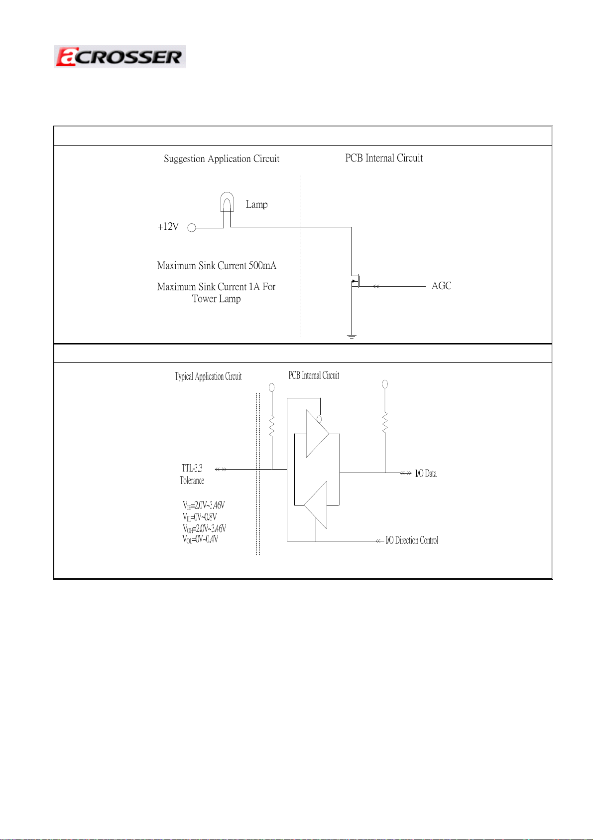
Revision: 1.0
3. O.D (Open-Drain) output external connection application note.
4. Spare IO (Spare Input/Output) external connection application note.
98
Page 99

Revision: 1.0
4 Acrosser Intelligent Reel Controller (AR-B2009)
This chapter's primary role is to distribute all of the best-known methods relating to the
design of an AGC (Acrosser Game Core) based reel controller. It provides implementation
details specific to Acrosser Intelligent Reel Controller Guide. The details of this document are
requirements for Acrosser Intelligent Reel Controller, unless the text explicitly states that a
design rule or connection is optional.
AR-B2009 Top-side:
AR-B2009 Bottom-side:
99
Page 100

4.1 Structure of Acrosser Intelligent Reel Controller
Application stack up
AIRP API
AIRP Driver
AGC / REEL Control
Motor Driver Board
Revision: 1.0
Physical Layer Block Diagram
REEL Mech
100
 Loading...