Acorn Products Z80 15, Z80 409 User Manual


Z80 SECOND PROCESSSOR SERVICE MANUAL
Part No. 0409,015
Issue 2
August 1984

Within this publication the term 'BBC' is used as an abbreviation for
'British Broadcasting Corporation'.
°Copyright Acorn Computers Limited 1984
Neither the whole or any part of the information contained in, or the
product described in, this manual may be adapted or reproduced in any
material form except with the prior written approval of Acorn
Computers Limited (Acorn Computers).
The product described in this manual and products for use with it, are
subject to continuous development and improvement. All
information of
a technical nature and particulars of the product
and its use (
including the information and particulars in this manual) are given by
Acorn Computers in good faith. However, it is acknowledged that there
may be errors or omissions in this manual. A list of details of any
amendments or revisions to this manual can be obtained upon request
from Acorn Computers Technical Enquiries.
Acorn Computers welcome
comments and suggestions relating to the
product and this manual.
All correspondence should be addressed to:-
Technical Enquiries
Acorn Computers Limited
Newmarket Road
Cambridge
CB5 8PD
All maintenance and service on the product must be carried out by
Acorn Computers' authorised dealers. Acorn Computers can accept no
liability whatsoever for any loss or damage caused by service or
maintenance by unauthorised personnel. This manual is intended only to
assist the reader in the use of this product, and therefore Acorn
Computers shall not be liable for any loss or damage whatsoever
arising from the use of any information or particulars in, or any
error or omission in, this manual, or any incorrect use of the
product.
This manual is for the sole use of Acorn Computers' authorised dealers
and must only be used by them in connection with the product described
within.
First published 1984
Published by Acorn Computers Limited

CONTENTS
Page
1 Introduction 1
2
Packaging and Installation
2
3
Specification
3
4 Disassembly and Assembly 4
5 Circuit Description 5
5.1 CPU
5
5.2 Clock
5
5.3 ROM Latch
5
5.4
Wait-States 6
5.5 Reset
6
5.6 Interrupt Handling
7
5.7 DRAM Control
7
5.8 DRAM Refresh
9
5.9 Desynchronising Logic
10
5.10 The Tube
11
6
Fault Finding on the Z80 Second Processor
17
6.1
General 17
6.2 Fault Conditions
17
6.3
Circuit Checks 19
Appendix
Diagnostic Flowcharts
25
Z80 Second Processor - Block Diagram
37
Circuit Diagram
39
Z80 PCB - Component Layout
41
Silk-Screen 43
Power Supply Unit - Circuit Diagram
45
Z80 Second Processor - General Assembly
47
Parts Lists - General Assembly
49
Z80 PCB Assembly
49

WARNING: THE Z80 SECOND PROCESSOR MUST BE EARTHED
Important: The wires in the mains lead for the. Z80 second processor
are coloured in accordance with the following code:
Green and yellow
Earth
Blue
Neutral
Brown
Live
As the colours of the wires may not correspond with the coloured
markings identifying the terminals in your plug, proceed as follows:
The wire which is coloured green and ye11ow must be connected to the
terminal in the plug which is marked by the letter E, or by the
safety earth symbol 4 or coloured green, or green and ye11ow.
The wire which is coloured blue must be connected to the terminal
which is marked with the letter N, or coloured black.
The wire which is coloured brown must be connected to the terminal
which is marked with the letter L, or coloured red.
If the socket outlet available is not suitable for the plug
supplied,
the plug should be cut off and the appropriate plug
fitted and wired
as previously noted. The moulded plug which was
cut off must bedisposed of as it would be a potential shock hazard if it were to be
plugged in with the cut off end of the mains cord exposed. The moulded
plug must be used with the fuse and fuse carrier firmly in place. The
fuse carrier is of the same
basic colour* as the coloured insert in the base of the plug. Different
manufacturers' plugs and fuse carriers are not
interchangeable. In the
event of loss of the fuse carrier, the moulded plug MUST NOT be used.
Either replace the moulded plug
with another conventional plug wired
as previously described, or
obtain a replacement fuse carrier from an
authorised BBC
Microcomputer dealer. In the event of the fuse blowing
it should
be replaced, after clearing any faults, with a 3 amp fuse
that is ASTA approved to BS1362.
*Not necessarily the same shade of that colour.

1. Introduction
This manual is intended to provide the information required to
diagnose and repair faults on the Z80 second processor (a part of the
BBC Microcomputer system) which was designed by Acorn Computers
Ltd.
of Cambridge, England.
The information contained in this manual is aimed at Acorn dealers and
service engineers who will be servicing the Z80 second processor on
behalf of Acorn Computers Ltd.
Z80 is a trademark of Zilog Inc.
CP/M® is a registered trademark of Digital Research Inc.
The Tube is a trademark of Acorn Computers Limited.

2. Packaging and Installation.
The Z80 second processor is supplied in a two-part moulded
polystyrene
packing which is further packaged within a cardboard
sleeve. Supplied
with the second processor is a DNFS ROM with fitting instruction
sheet, a set of reminder cards for the red function keys, 7 floppy
disks, an end-user licence and a guarantee card. For BBC
Microcomputers fitted with MOS ROMs below version 1.2, a voucher
redeemable against replacement of lower version
ROMs, is also
supplied.
Note: Care should be taken when unpacking and repacking this unit to
ensure that all items are positioned correctly, especia11y the floppy
disks which should first be packed in plastic bags and laid flat.
The Z80 Second Processor User Guide and accompanying literature is
supplied packed separately.
A mains power switch is located at the rear of the second processor.
A 250mA. type T (slow blow) fuse is located at the rear of the second
processor. Before removing this fuse, the second processor must be
disconnected from the mains supply. Access to the fuse may
be gained
by undoing the round cover with the slot in it using a
screwdriver.
The mains supply must not be reconnected until the fuse is relocated
in its holder with the cover screwed home.
Do not use the second processor in conditions of extreme heat, cold,
humidity or dust, or in places subject to vibration. Do not block the
ventilation under or behind the second processor. Ensure
that no
foreign objects are inserted through any openings in the
second
processor.

3. Specification
3.1 The Z80 second processor
A second processor for the BBC Microcomputer model B, operating
through the Tube, providing the ability to run sophisticated software
under the CP/M 2.2 operating system.
The second processor is housed in a rigid injection moulded
thermoplastic case and contains the fo11owing:
A 6MHz Z80B CPU
64K of read/write Random Access Memory
4K Read Only Memory ("shadow ROM") providing a boot function on powerup and to handle Non-Maskable Interrupts (NMI) from the Host
processor
via the Tube.
The Tube - a fast asynchronous communication path connecting the
second processor to the I/O processor (BBC Microcomputer).
A mains-operated integral power supply comprising a mains transformer
and power supply board.
3.2 Power Supply
Max. AC Input
264V AC
MIN. AC Input 216V AC
Power Rating
14 watts
Supply Frequency
47-63Hz
Max. Output Current lA at +5V

4. Disassembly and assembly
To service the Z80 second processor, disconnect it from the BBC
Microcomputer and the mains supply and undo the three fixing screws;
two at the top of the back panel and one underneath the unit, nearest
the front and equidistant between the two rubber feet. (The assembly
diagram is given in the Appendix). The lid can now be removed
revealing the transformer and power supply
board, held in place by six
screws, and the Z80 PCB. It is recommended
that the transformer and power supply board are not removed unless
absolutely necessary.
To remove the Z80 PCB from the case, pu11 off the two "fast on" tabs
which connect the power supply (brown +5v and black 0v leads) and
remove the four screws which hold the PCB in place.

5. Circuit Description
The circuit may be split into a number of sections by their specific
function. These are dealt with under separate headings.
Reference
should be made, where necessary, to the block diagram and
circuit
diagram in the appendix.
5.1 CPU
The microprocessor used in this unit is a Z80B, running at a clock
frequency of 6MHz from a crystal oscillator. A11 memory and I/O cycles
are performed at fu11 speed, with the exception of those to the "boot"
ROM, for which a Wait-State is inserted by external logic.
5.2 Clock
A 12MHz crystal controls the frequency of the oscillator formed by the
inverters 1C 24D,E. A "D" type latch, IC17A, is used to divide the
frequency to the required 6MHz. Transistor Q1 provides an active pullup for the clock signal, after inversion by IC 24B, to
compensate for
the high dynamic input current of the Z80 on this
signal. The NAND
gate IC19D and associated network , provide a shaped clock signal for
the "NMI Service Detect" logic. Since the output of the "D" latch is
inverted before being used as CPU clock,
then the "D" output is
available for use as an inverted clock by
the DRAM control and the
desync. logic.
5.3 ROM Latch
The Z80 second processor features a "shadow" ROM to boot the system
upon power-up and also to ensure proper handling of NMI interrupts
from the host processor via The Tube. The ROM is enabled at the
proper
times by the latch IC15A.
1.
After power-up, the reset signal from IC24F to the Z80 is used
to
clock the latch IC15A and produce the ROM signal. On any memory read
cycle, while the Rom signal (TP2) is active, IC22B&C
wi11 produce an
output-enable signal to the ROM (IC3 pin 20).
The initial instructions following RESET are executed from ROM and
initiate the copying of ROM into high RAM. This is followed by an
instruction-fetch cycle to memory over 8000H which is detected by the
AND gate IC20B and used to clear the ROM latch, remove the
shadow ROM
from the memory-map, and allow normal running in RAM.
2.
The NM1 signal to the Z80 processor is used by system software in
Disc handling, however, the Z80 interrupt vector to 66H is not
compatible with standard CPM, which has its default file-control block
in this area. The solution used is to bring the shadow ROM
temporarily
into the memory-map when an instruction fetch from 66H
is detected. IC26 and IC27 provide a clock signal, NMISERV during such
a cycle, which presets the ROM latch IC15A, latching the ROM in until
an instruction-fetch from high RAM. In the ROM, 66H contains a jump to
the destination expected by standard CPM.
Because of the slow access time of the "boot" ROM, all memory cycles
to the ROM must be lengthened by the insertion of a "Wait-State" of
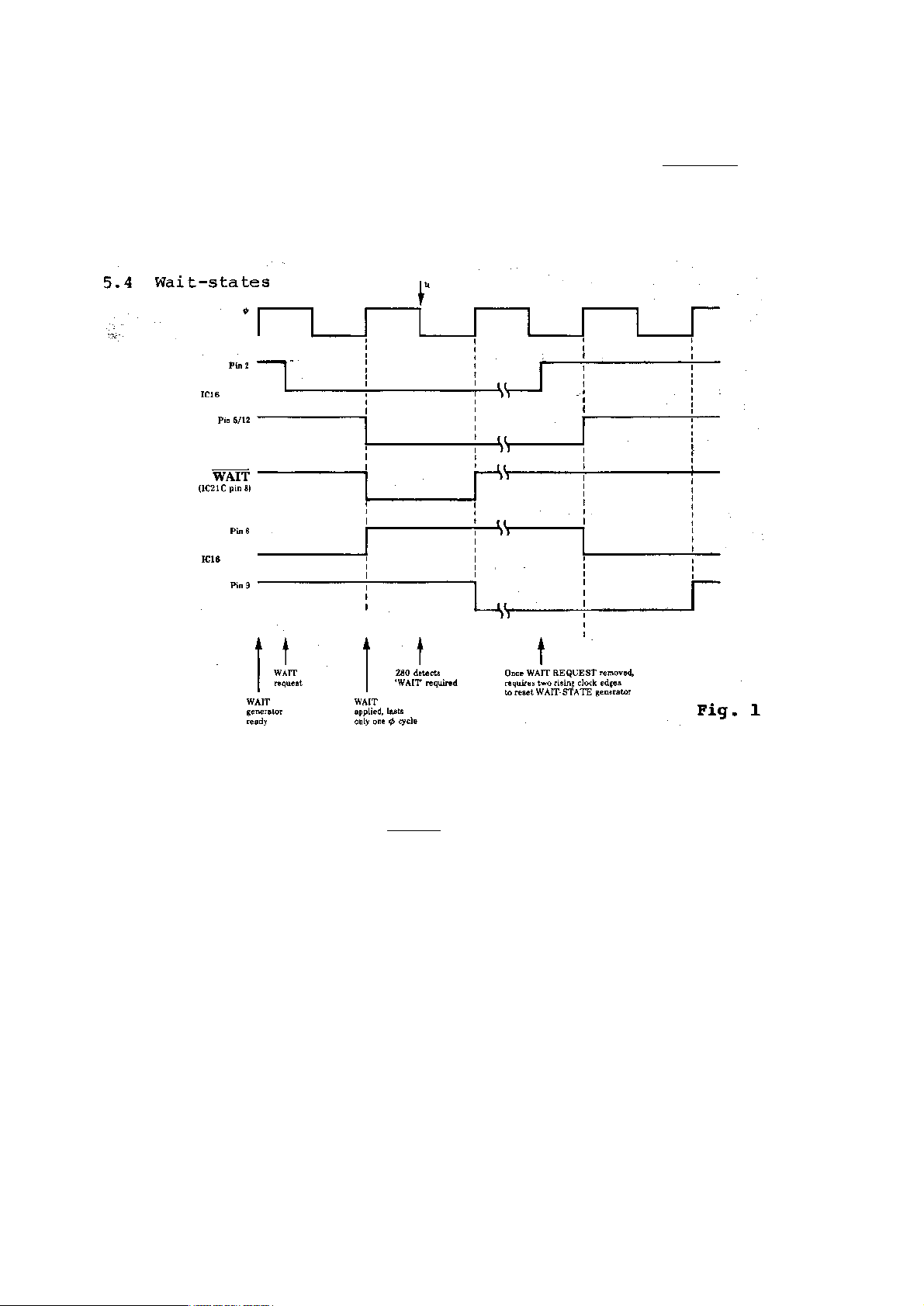
one clock cycle. When the ROM is selected, the OR
gate IC22C provides
the OE signal to the ROM and this is used to
enable the Wait-State
generator IC16A&B. Via the
NAND gate IC21C,
a low-going pulse of 1
clock cycle is fed to the WAIT input of the Z80 (see timing diagram
above). The Wait generator requires a further two clock cycles after
the end of the lengthened memory
cycle to clear itself. The Z80 samples the WAIT input on the
falling edge of 0 (t1). TP7 a11ows observation of the WAIT signal.
5.5. Reset
The Z80 second processor may be reset at any time, by the host
processor via the Tube.
The Z80 requires that a reset signal should not occur immediately
after an instruction fetch cycle, otherwise corruption of DRAM data
might result. To avoid this, the "D" latch IC15B synchronises the
reset signal from the Tube to the beginning of an
instruction-fetch
cycle (M1). A monostable IC14 ensures the reset

signal to the CPU is a pulse of approx. 4µs duration, sufficient to
produce a reset without delaying the refresh to the DRAMS and so
losing data. The reset to the CPU also clears the ROM latch IC15A,
bringing the shadow ROM into the memory-map.
The Schmitt NAND gate IC19C provides a Power-Up reset to' the Z80 from
the delay network R1, C2 (time-constant 100ms). Diode D1 ensures that
the capacitor does not apply a reverse voltage to the NAND gate input
on Power-Down.
5.6 Interrupt Handling
The host processor can interrupt the Z80 with a maskable interrupt via
the Tube. The interrupt output from the Tube is taken directly to the
INT input of the Z80. After detection of an interrupt, the
CPU M1 and
IORQ outputs go low to indicate a vector for the
interrupt is expected
on the data bus D0 to D7. The buffer IC28 is enabled by M1 and IORQ
and its inputs are permanently tied to logic 0 or 1 to give a vector
address of 0FEH. The Z80 'Boot' ROM places the Z80 internal interrupt
system into Mode 2, with a High-Byte address of OFFH, giving an
address for the interrupt vector of 0FFFEH.
5.7 DRAM Control
5.7.1 Read/Write Cycles
a.
RAS
Whenever a memory cycle occurs, the preset signal on the "D" latch
IC17B is removed by the MREQ signal from the Z80. On the next rising
edge of the system clock, the "D" latch output goes low, giving the "
CHOP" signal. During memory read or write cycles, the fa11ing edge of
CHOP produces the row-address (RAS) signal (TP8), via IC20A, to the
DRAMS, causing the row address information to
be latched by the RAMS.
Prior to the RAS signal, the row-address buffer 1C5 was enabled by the
high level on RAS and consequently
the low level on the inverted RAS
signal from 1C21A, thus allowing the low order address lines A0 to A7
to be passed to the DRAMS.
Once RAS goes low, IC5 is disabled and IC4
enabled, to allow the
column address through to the DRAMS. The
inverter IC25E ensures a
slight delay in the enabling of the Column
buffer, to avoid data
conflict with the Row buffer.
b.
CAS
The column-address signal to the DRAMS is generated from the RAS
signal by the OR gates IC23C&D. If the shadow ROM output-enable signal
is active, then the CAS signal wi11 not be generated (logic
1 on pin
12 - IC23D). The AND gate 1C20C enables or disables the
CAS signal
under certain other conditions.
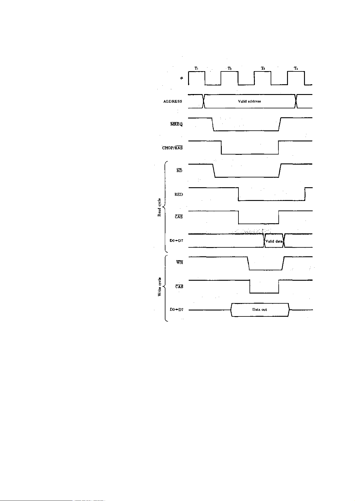
Fig. 2 RAM read or write cycles
CAS is enabled if:
i. the memory cycle
is a
write cycle
(WR
low, to IC20C
pin
11).
or ii. the memory cycle
is
a read cycle and
not an
instruction-fetch
cycle (IC18B not
preset by Ml, RED
signal to IC20
pin 9).
or iii. the cycle is an
instruction-fetch
this signal being
synchronised to
the CPOP signal
by
OR gate 1C23B (to
IC20 pin 10)
Note: In this case, the
CAS signal will
not be generated
if the ROM is
selected.
5.7.2 Instruction-Fetch Cycles
The Z80 CPU handles an Instruction Fetch differently to other memory
read cycles, in that the MREQ signal is active for only 1.5 clock
cycles instead of 2. In order to allow sufficient access time for the
DRAMS in this abbreviated cycle, the
Instruction-Fetch signal, Ml, is
used to generate the RAS and CAS
signals a half-cycle earlier. The OR
gate IC23A allows the clock
signal through to the "D" latch IC18A,
only when M1 is active. The output of the "D" latch, SUE is clocked
low, and generates the
row-address latch signal RAS, a half clock
cycle before the CPOP signal would have done. When the CPOP signal
arrives after being
generated by the MREQ (see section 5.7.1a), it
clears the SUE
latch and holds RAS low itself until MREQ becomes
inactive.
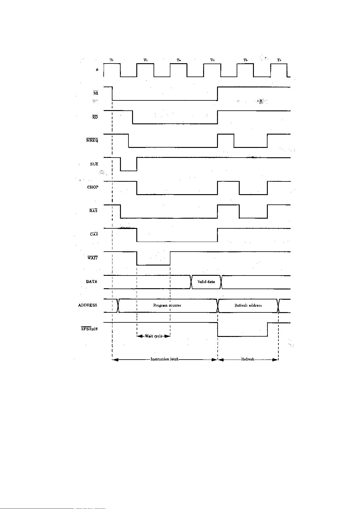
Fig. 3 Instruction-Fetch cycles
5.8 DRAM Refresh
After each instruction-fetch, the Z80 CPU performs a Refresh cycle for
the DRAMS in the period while the instruction is being decoded. A
seven-bit refresh address is output onto the address-bus (A0 to A6, A7
=0) for approx. 2 clock cycles, and the MREQ signal goes
low.
The "
RFSH" signal from the Z80 is not used, and no other
memory control signals go active. The Refresh address is incremented
by the CPU after each time.
Once the MREQ signal goes active, the "D" latch 1C18B produces CPOP
and hence RAS as normal. The CAS is not required for a Refresh
cycle,
and is not enabled since none of the conditions listed in section 5.7.
1b are true (AND gate IC20C).
When the shadow ROM is being read, the CAS signal to the DRAMS
is
disabled, but the row-address latch signal, RAS, sti11 occurs. This
has the effect of a refresh cycle to the DRAMS.
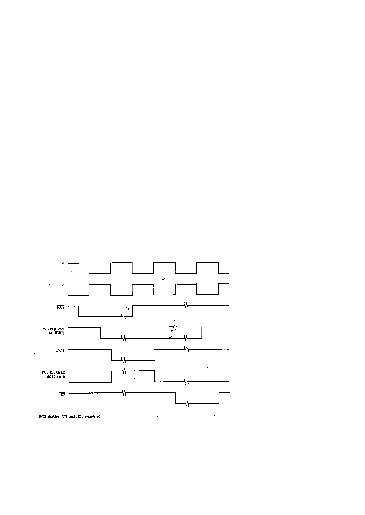
5.9 Desynchronising Logic
To prevent ambiguous events, i.e. a register status change during
a
status read, this circuit produces a "WA1T" signal to the Z80
processor when the PCS and HCS signals occur simultaneously.
When this happens, a low signal from IC29B pin 6
appears at IC30A
pin
2. Q on IC30A goes high and, via IC29A, maintains a logic 1
signal
upon pin 12 of IC30B, thus, by the end of one clock cycle a
high is
sent from pin 9 of IC30B to disable PCS. Simultaneously, a WAIT signal
is generated for the second processor via IC19A&B.
As soon as HCS (TP6) is removed, the next rising clock edge
removes
the WAIT signal from the Z80 and, as PCS is still low, a
low signal is
sent
through IC30B to
the
Tube. This is then
maintained by the
low signal upon pin
4
of IC30A until the
PCS is
complete.
Thus, if PCS (TP5)
is already running,
it will continue
despite an HCS, but
if HCS began first
then PCS is
prevented from
acting.
*At no time is PCS
affected, as it
would not be
possible to 'stop'
the BBC processor.
Fig. 4 Timing Diagram - HCS/PCS
5.10 The Tube
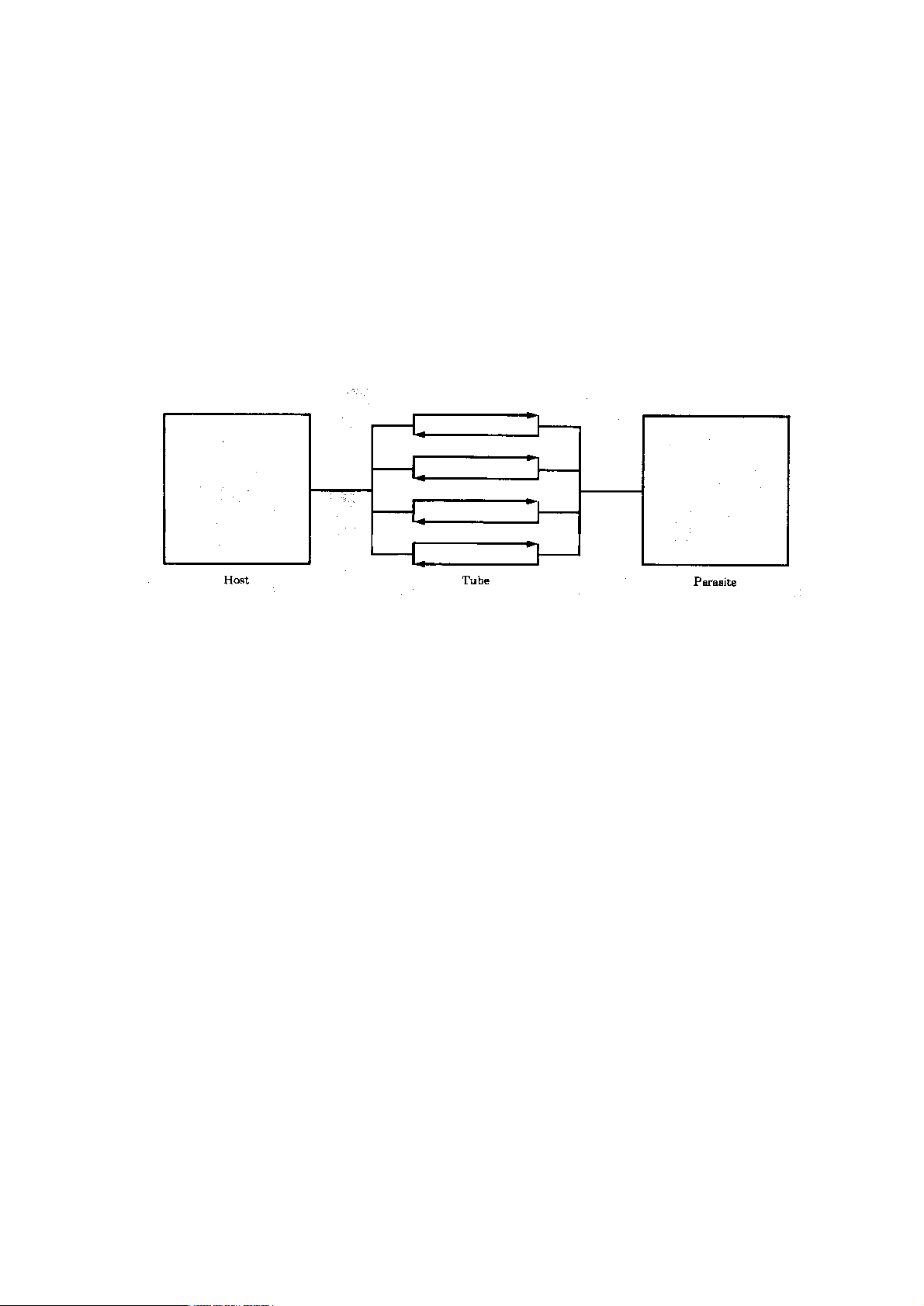
The Tube (IC1) is an Acorn custom IC which provides parallel
asynchronous communication between two processor systems, the BBC
Microcomputer (Host) and the Z80 second processor (Parasite).
To
each
processor system, it resembles a conventional peripheral device
comprising 4 read-only and 4 write-only, 8-bit registers. The Z80
accesses these registers via its I/O structure.
Fig. 5 Tube concept
5.10.1 Tube Registers
Each register has its own status byte, with a separate I/O address,
containing Register-Fu11 and Data-Available flags. The status byte for
Register 1 contains additional control bits that may be set by the
Host computer to enable interrupts or to reset the Z80. These control
bits may be read, but not set, by the second processor.
Fig. 6 shows the Tube registers in more detail
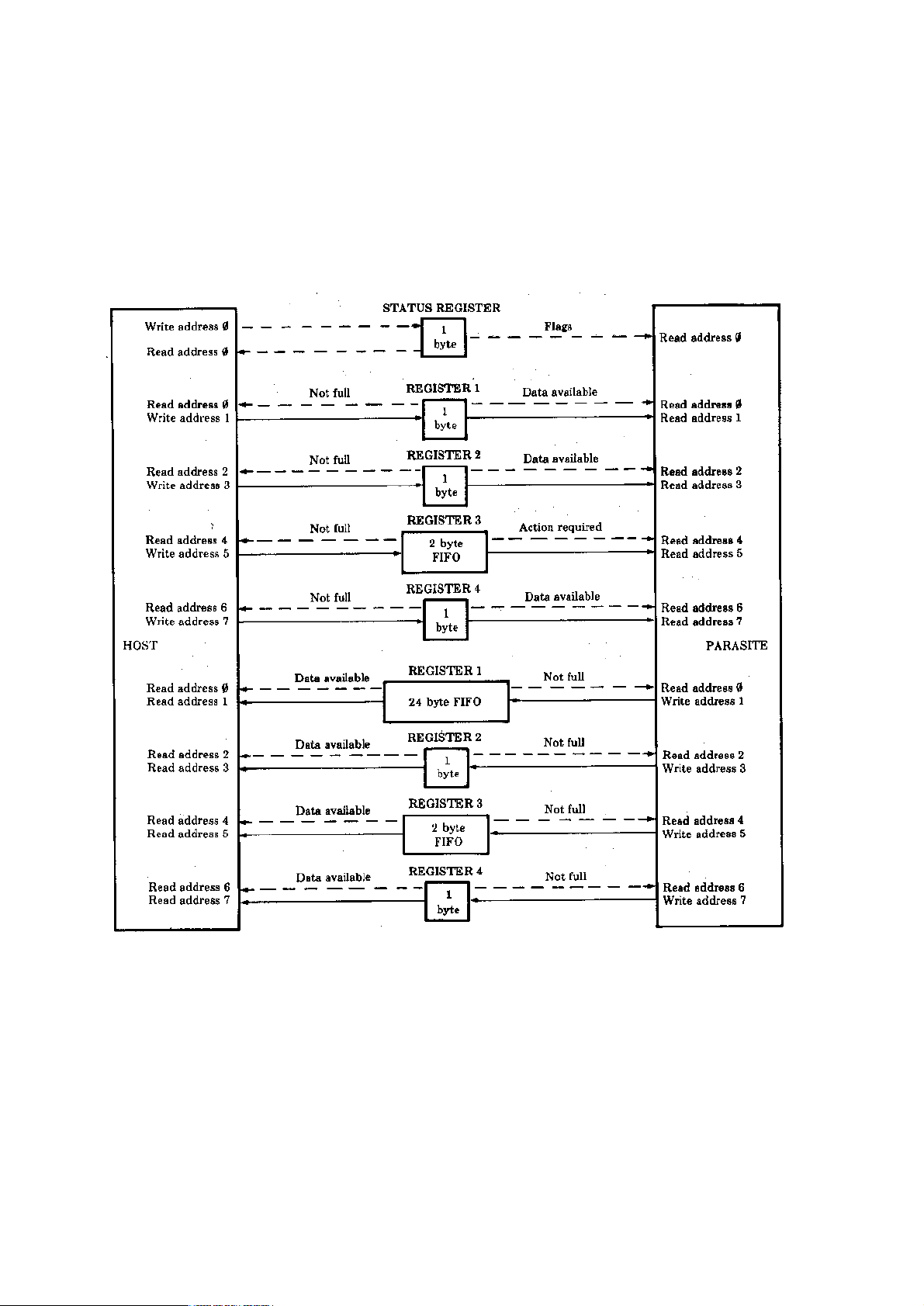
Fig. 6 Schematic diagram of Tube registers
 Loading...