

Aconno ACN52832 User Manual

D A T A S H E E T
ACN52832
Fully integrated, ultra-low power, Bluetooth Smart module
IoTmade easy

aconno.de
August 11, 2017
Datasheet
aconno ACN52832 V1.2
The ACN52832 is a fully integrated, ultra-low power, Bluetooth Smart (former BLE) module
in a small form factor which features the advanced Nordic Semiconductor nRF52832 SoC.
Its capabilities are tailored for the upcoming demands of sophisticated IoT devices where
small size, low power, application performance and radio-range are essential.
Unlike many competitors it features a maker-friendly PCB scale package which allows a fast
and easy integration without sacrificing access to its advanced peripherals and capabilities.
The ACN52832 features a large number of GPIOs. Thanks to an on-board antenna its RF
performance is excellent. To provide quick access to the programming interface of the SoC,
the module also features a Tag-Connect connector.
The information contained in this document is the prope rty of aconno GmbH and should not be disclosed to any third party with out written permission.
Specification subject to change without notice. © aconno GmbH 2016
2

aconno.de
August 11, 2017
Table of Contents
1.Overview and Features .................................................................................................. 4
2.Applications ................................................................................................................... 4
3. Block Diagram ............................................................................................................... 5
4. Pin Description .............................................................................................................. 6
5. Module Specifications ................................................................................................... 9
5.1 Absolute Maximum Ratings ................................................................................................ 9
5.2 Recommended Operating Conditions ................................................................................ 10
5.3 Current Consumption ........................................................................................................ 11
5.4 Clock Sources .................................................................................................................... 12
5.5 Radio Specifications .......................................................................................................... 12
5.6 GPIO Specifications ........................................................................................................... 13
6. Electrical Schematic .................................................................................................... 14
7. Mechanical Outlines.................................................................................................... 15
7.1 Marking on metal shielding ............................................................................................. 15
8. Firmware .................................................................................................................... 17
8.1 S132 BLE SoftDevice .......................................................................................................... 18
8.2 S212 ANT SoftDevice ......................................................................................................... 19
9. Programming / Flashing with Tag Connect ................................................................... 20
10. Certification .............................................................................................................. 21
10.1 FCC (USA) ....................................................................................................................... 21
10.2 IC (Canada) ..................................................................................................................... 23
11. Revision History ........................................................................................................ 24
12. Contact Information .................................................................................................. 25
The information contained in this document is the prope rty of aconno GmbH and should not be disclosed to any third party with out written permission.
Specification subject to change without notice. © aconno GmbH 2016
3

aconno.de
1. Overview and Features
● Based on Nordic Semiconductor’s
nRF52832 Bluetooth Smart SoC
● 32-bit ARM® Cortex™ M4F high performance 64 MHz
processor core with
512kB Flash / 64 kB RAM
● On-board precision 32 MHz and 32.768 kHz crystal
clocksources
● Tag-Connect SWD easy-to-use programming interface
● Up to 28 GPIOs with flexible module pin mapping
● Programmable peripherals for CPU-less operation
● SPI / UART / TWI (I
2
C)
● 200 ksps 12-bit ADC
● Low Power Comparator
● I²S and PDM peripherals for Audio
● Quadrature demodulator
● RGB LED
● Fully tuned RF on-board antenna for excellent
performance and range
● -20 dBm to +4 dBm output power
● Ultra-low power consumption
● Dimensions: 20.2 x 25 x 3 mm
● Temperature Range: -40°C to +85°C
● Wide supply voltage range: 1.7V to 3.6V
● 3V Lithium battery supported
● NFC-A tag for OOB Bluetooth Smart pairing and wakeup
on field
● Multiprotocol 2.4 GHz radio
2. Applications
IoT connected devices
Bluetooth Smart Sensors
Home Automation and Control
Lighting
Beacons
Battery driven applications such as
wearables
August 11, 2017
The information contained in this document is the prope rty of aconno GmbH and should not be disclosed to any third party with out written permission.
Specification subject to change without notice. © aconno GmbH 2016
4

aconno.de
August 11, 2017
3. Block Diagram
The heart of the ACN52832 module is Nordic’s highly integrated nRF52832 BLE SoC which
contains a 2.4 GHz transceiver, a 32-bit ARM® Cortex™-M4F CPU, a 512 kB flash memory, 64
kB RAMas well as analog anddigital peripherals.
It can support BLE, ANT/ANT+ and a range of proprietary 2.4 GHz protocols through so called
SoftDevices from Nordic Semiconductor, which can be downloaded freely from Nordic’s
website.
Ultra low power consumption and advanced power management enables a battery lifetime
up to several years on a coin cell battery. The 20.3 x 25 x 3 mm sized module integrates
power supply decoupling capacitors, 32 MHz and 32.768 kHz crystals, load capacitors, a DC-
DC converter, a RF matching circuit and an antenna in addition to the wireless SoC.The
module also features a small RGB LED for optical feedback.
Solely the addition of a suitable DC power source is necessary for BLE and/or ANT
connectivity. As a result of its Tag-Connect capabilities, the ease of application is further
increased. Sensor applications require additional appropriate sensors.
NFC functionality requires anexternallyconnected antenna.
The information contained in this document is the prope rty of aconno GmbH and should not be disclosed to any third party with out written permission.
Specification subject to change without notice. © aconno GmbH 2016
5

aconno.de
August 11, 2017
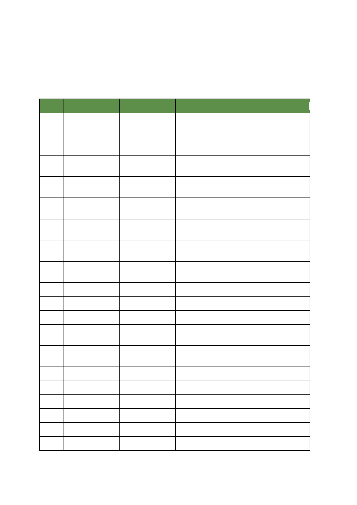
4. Pin Description
The module uses a user-friendly PCB with surrounding solder pads (1.4 mm pitch) in order to
provide flexible, “through hole mounting” for rapid prototyping or, furthermore, a SMD
mounting technique for a permanent implementation.
The information contained in this document is the prope rty of aconno GmbH and should not be disclosed to any third party with out written permission.
Specification subject to change without notice. © aconno GmbH 2016
6
aconno.de
Pin
Name
Pin function
Description
1, 13,
35
GND
Ground
Should be connected to the ground potential of the
application board
12, 23,
24, 32
VDD
Power
Power supply (1.7 V – 3.6 V)
33
SWDIO
Digital I/O
Serial Wire Debug I/O for debugging and
programming
34
SWDCLK
Digital Input
Serial Wire Debug clock input for debugging and
programming
9
P0.02 / AIN0
Digital I/0
Analog In
GPIO / Analog Input 0
10
P0.03 / AIN1
Digital I/0
Analog In
GPIO / Analog Input 1
11
P0.04 / AIN2
Digital I/0
Analog In
GPIO / Analog Input 2
14
P0.05 / AIN3
Digital I/0
Analog In
GPIO / Analog Input 3
15
P0.06
Digital I/O
GPIO
16
P0.07
Digital I/O
GPIO
17
P0.08
Digital I/O
GPIO
18
P0.09 / NFC1
Digital I/O
NFC
GPIO / Connection to NFC-coil
19
P0.10 / NFC2
Digital I/O
NFC
GPIO / Connection to NFC-coil
20
P0.11
Digital I/O
GPIO
21
P0.12
Digital I/O
GPIO
22
P0.14
Digital I/O
GPIO / Trace Data 3
25
P0.15
Digital I/O
GPIO / Trace Data 2
26
P0.16
Digital I/O
GPIO / Trace Data 1
27
P0.17
Digital I/O
GPIO / Trace Data 0
August 11, 2017
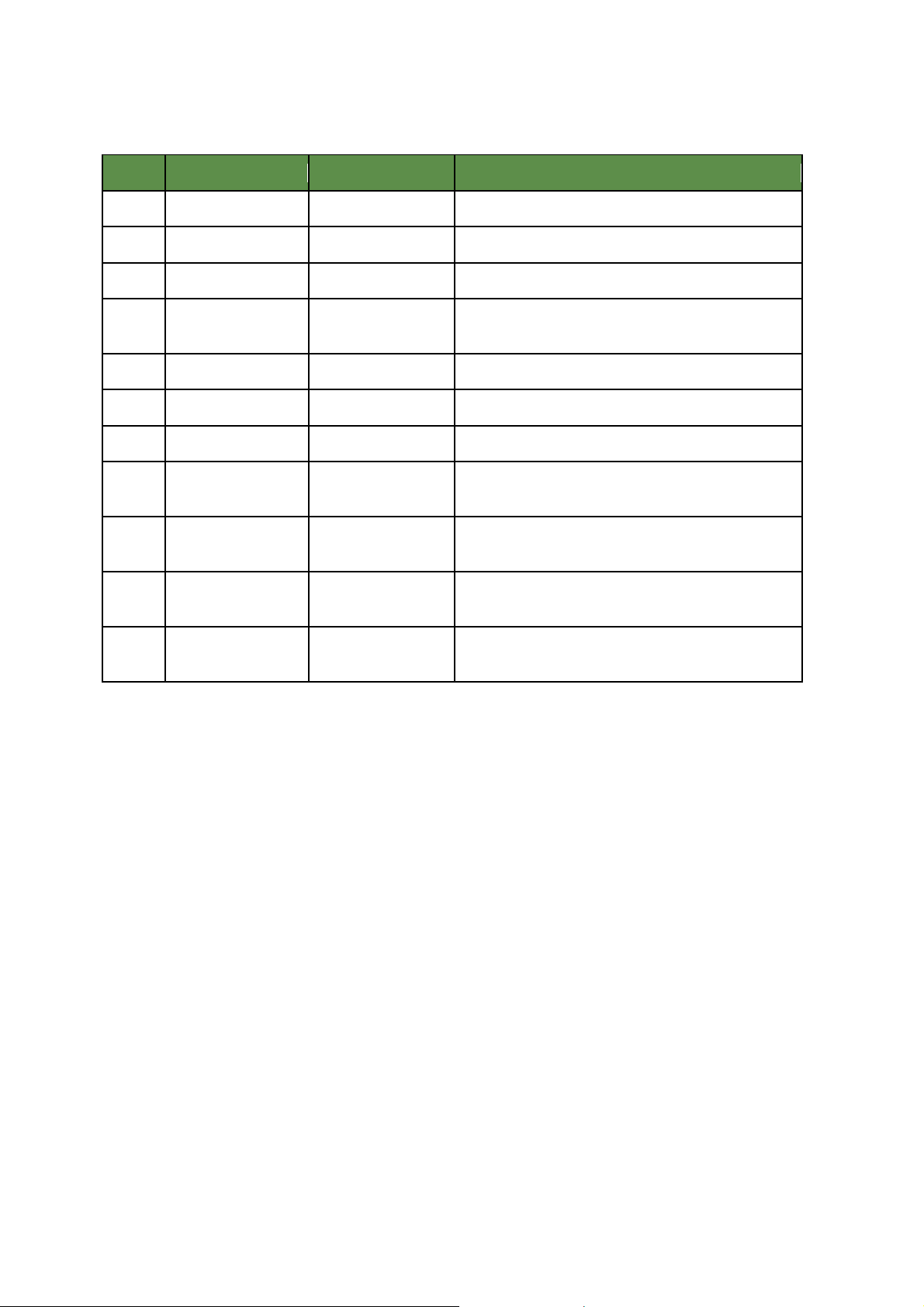
I/O Pins sorted by port name:
The information contained in this document is the prope rty of aconno GmbH and should not be disclosed to any third party with out written permission.
Specification subject to change without notice. © aconno GmbH 2016
7
aconno.de
Pin
Name
Pin function
Description
28
P0.18
Digital I/O
GPIO
29
P0.19
Digital I/O
GPIO
30
P0.20
Digital I/O
GPIO / Trace Clock
31
P0.21
Digital I/O
RESET
GPIO / System Reset / Low Drive / Low Frequency
2
P0.25
Digital I/O
GPIO / Low Drive / Low Frequency
3
P0.26
Digital I/O
GPIO / Low Drive / Low Frequency
4
P0.27
Digital I/O
GPIO / Low Drive / Low Frequency
5
P0.28
Digital I/0
Analog In
GPIO / Analog Input 4 / Low Drive / Low Frequency
6
P0.29
Digital I/0
Analog In
GPIO / Analog Input 5 / Low Drive / Low Frequency
7
P0.30
Digital I/0
Analog In
GPIO / Analog Input 6 / Low Drive / Low Frequency
8
P0.31
Digital I/0
Analog In
GPIO / Analog Input 7
August 11, 2017
The information contained in this document is the prope rty of aconno GmbH and should not be disclosed to any third party with out written permission.
Specification subject to change without notice. © aconno GmbH 2016
8
 Loading...