

Page 1

FES7035
User Manual
FES7035: Fanless Embedded System Atom D2550
Dual Core 1.86GHz Processor
14628 Central Ave,
Chin o, CA 91710
tel: 909.597.7588, fax:909.597.1939
Fanless Embedded System
© Copyrigh t 2013 Acnodes, Inc.
All rights reserved. Product description and product specifi cations
are subj ect to chan ge without noti ce. For latest product informati on,
please visit Acnodes’ we b site at www.acnodes.c om.
Page 2

Copyright
This publi cati on c ontains inform ation that is prot ected by copyright. N o part of it m ay be reproduced i n
any form or by any m eans or used to make any transform ation/adaptation without the prior written
permission from the copyr ight holde rs. The manufacturer reserves the right to revise this publication and
m ake changes to its contents at any time, w ithout obl igation to noti fy any person or entity of such
revisions or changes.
©201 3. Al l Rights Reserved.
Trademarks
Al l tradem arks and registered trademarks of products appearing in this m anual are the properties of their
respective holders.
Notice:
1. The chan ges o r modifica tion s n ot expressly a ppro ved by th e p arty r espo nsible fo r compliance cou ld void th e user ’s auth ority
to op erate t he eq uipment .
2. Shielded int erfa ce ca bles must be used in or de r to comply wit h t he emission limits.
Static Electricity Precautions
It is quite easy to inadvertently dam age the system board, c omponents or devices e ven before i nstal ling
them i n your system unit. Static electri cal discharg e can dam age computer com ponents wi thout causing
any signs of physi cal dam age . You must take extra care in handl ing them to ensure against el ectrostatic
bui ld up.
1. To prevent electrostatic bui ld up, le ave the system board i n i ts anti-static bag unti l you are ready to install
it.
2. Wear an antistatic wrist st rap.
3. Do all preparation w ork on a stati c-free surface.
4. Hold the device only by its edges. Be careful not to touch any of the components, contac ts or
connections.
5. Avoi d touching the pins or contacting all m odul es and connectors. Hold modules or connectors by the ir
ends.
Impo rt ant:
Elect rost atic d ischa rge (ESD) can damage you r p rocessor, disk dr ive an d ot her compo nents. Perform t he up grade instru ct ion
pr ocedures describ ed at an ESD wor kstation on ly. If such a sta tion is no t availab le, yo u can provide some ESD protection by
wear in g a n ant istatic wrist st rap and attaching it to a met al part of the system chassis. If a wr ist strap is una vailab le, es tab lish
an d maintain contact with the syst em chassis th roug hout any p rocedures req uiring ESD protection .
Page 3

FES7035
Safety Measures
Fanless Embedded System
To avoid dam age to the system :
• Use the correct A C input vol tage range to reduce the risk of ele ctric shock.
• Unplug the power cord before rem oving the system chassis cover for install ati on or servi cing. After
instal lation or servicing, cover the system chassis bef ore plugging the power cord.
Batte ry:
• Dange r of expl osion if battery incorrectly replaced.
• Repl ac e only w ith the same or e quival ent type re com mend by the manufacture r.
• Dispose of used batteries according to l ocal ordinance.
Warranty
1. Warranty does not cover dam ages or fai lures caused by m isuse of the product, inabili ty to use the
product, unauthorized replacem ent or any kind of alterations of components and product
specif ications.
2. The warranty i s voided if the product has been exposed to physi cal abuse , improper instal lation, a ny
kind of modific ation, acc idents or unauthorized repair of the product.
3. Unl ess otherwise instructed in this user m anual, the user m ay not, under any ci rcum stances, attem pt to
perform servi ce , adjustm ents or repairs on the product him se lf, whether the product is sti ll covered by
warranty or not. It must be returned to the place i t was purchased at, the fa ctory or an authorized
se rvic e agency for any re pai r work.
4. We w il l not be l iabl e for any indi re ct, spe cial, incidental or conseque nt damages to the product that has
be en m odif ied or alte red.
14628 Central Ave,
Chin o, CA 91710
tel: 909.597.7588, fax:909.597.1939
© Copyrigh t 2013 Acnodes, Inc.
All rights reserved. Product description and product specifi cations
are subj ect to chan ge without noti ce. For latest product informati on,
please visit Acnodes’ we b site at www.acnodes.c om.
Page 4

FES7035
Copyright ..................................................................................................................
2
Trademarks ...............................................................................................................
2
Stati c Electric ity Precautions ....................................................................................
2
Safety Measures .......................................................................................................
3
Wa rranty ........................................................... ........................................................
3
Fanless Embedded System
Chapter 1: Introduction
1 -1 O verview.............................................................................................................. 5
1 -2 P roduct Specification........................................................................................... 6
1 -3 System Block Diagram ......................................................................................... 8
1 -4 M echanical Diagram ........................................................................................... 9
1 -5 Front and Rear I/O …............................................................................................ 10
Chapter 2: Pin D efinition & Jumper Settings
2 -1 Front panel Pin Definiti on………………………………… ……… ………….............…… ……… 11
2 -2 Rear Panel P in Defi nition………………………………… ……… ……………………………………. 12
2 -3 Internal P in Defi ni ti on & Jum pe r Settings… ……………………………………………………. 16
2-3 .1 Main Board Top V iew ………………………….………………………………………… …… . 16
2 -3.2 M ain Board Pin Definition & Jumper Settings……………… ………………………. 17
2 -3.3 Jum per Settings……… .………………………….……………………………………… ………. 23
2 -4 G PRS Board P in Definition & Jum per Settings………….……………… ………………………. 26
Chapter 3: Software Support G uide
3 -1 Dr iver Installation……………….………………… …………… …………………………………………. 30
3 -2 G PRS M odule Software Program ming…………………………… ……………………………… 30
Chapter 4: BIOS Setup Menu
4 -1 BIOS Configuration Overview ……… …………………………………………………………………. 36
4 -2 Entering BIO S Setup…………………………………… …………… ……………………………………… 36
4 -3 A dvanced CMOS Features… …………………………………………… ………………………………… 39
4 -4 Other BIO S Features……… …………… ..…………………………………………………………………. 46
4 -5 Security Features ….……..………………………………… ……… ………………………………….….. 47
4 -6 Boot M anagem ent Setup ..…………………… ………………………………………..……………... 48
4 -7 Exit BIOS Setup ……………………… .……..…………………………………………………….……..…. 49
Appendix A: GHOST Recovery Guide …………………………………………………………………… 50
Appendix B: M 12 USB Connector De finition for Lab Test..…………………………………… 56
14628 Central Ave,
Chin o, CA 91710
tel: 909.597.7588, fax:909.597.1939
Table of Contents
© Copyrigh t 2013 Acnodes, Inc.
All ri ghts reserved . Produ ct descri pti on an d produ ct specificati ons
are subj ect to chan ge without noti ce. For latest product informati on,
please visit Acnodes’ we b site at www.acnodes.c om.
Page 5

FES7035
Chapter 1: Intr
1-1 Overview
oduction
Fanless Embedded System
Acnodes’ FES 703 5 i s an outstanding and reliable embedded system with high perform ance and low
powe r consumption re mained.
FES703 5 has applied w ith the Atom D2 550 dual -core 1.86 G Hz processor wi th NM 10 South Bridge chipset,
which not only del ivering hi gh performance i n m ulti -m edi a capabili ty but also provi ding high speed storage
inte rface as to inc rease the processing efficie ncy. More over, the m em ory capaci ty allows reachi ng up to
4GB DDR3 800 /106 6 at the max imum. For the disk drive storage, it is designed with 2.5” SATA HDD and
one Mini-PCI-E mSATA.
In orde r to m eet the netw ork stabi li ty, FES 70 35 use two Re al tek 81 xx 10 0/1 000 Mbps L AN with Wake-On
L AN & DMI to support and maintai n Etherne t function. The system designed w ith two DB-9 supports for
RS-232/ 42 2/ 485 and w ith tw o DB-9 supports for RS-2 32 interface, whic h coul d be opti onal ex pand to six
COM s. It also provides a software programm ing Watchdog ( WDT) with time r range from 1 to
255 seconds. For the audi o output, there has occupied w ith an A LC 6 62 for speaker.
FES 7035 is equi pped w ith graphic core with 64 0 Mhz for supporting its graphi c solut ion; displ ay functi on
supports for dual displ ay by DVI-I +DVI-D . For DVI and VGA display, it supports for 192 0 x 1200 resoluti ons .
FES 703 5 has also designe d w ith ex pansion flexibil ity for one PCI-104 modul e and two M ini-PCI-E expansion
slots avai lable .
FES 7 035 supports G PRS function with 3 .5 G Wire less Mobi le , which supports for GSM , GPRS, EDGE,
WCDMA and HSDPA. The outstanding fl ex ibili ty enables to support tri -band or quad-band. More
im pressive ly of FES 703 5 platform i s equi pped with the M 12 conne ctor. The re are tw o of the M12
connector for USB and two for LA N ports in order to em pow er feature in anti-vi bration and anti -dust. The
FES 70 35 also offe rs optional full syste m anti -vibration protection, whi ch helps to i mprove the system
stability and quali ty whi le w orki ng under railway environment.
The powe r is able to accept a wide DC power input ranging from 6 V to 34V. The powe r consum pti on can
reach up to 22 W in m ax imum. T he system is valuable for al l the em bedde d appli cati ons, and also w ell
support with the W indow 7, W indows XP and Linux Operati on system .
14628 Central Ave,
Chin o, CA 91710
tel: 909.597.7588, fax:909.597.1939
© Copyrigh t 2013 Acnodes, Inc.
All rights reserved. Product description and product specifi cations
are subj ect to chan ge without noti ce. For latest product informati on,
please visit Acnodes’ we b site at www.acnodes.c om.
Page 6

1-2 Pr
oduct Specificati
on
Processor
Sup port Atom D2550 Du al-Core 1.86 GHz Proc esso r
Atom N2800 Dual-Core 1.86 GHz
Atom N2600 Dual-Core 1.6 GHz
Processor
Processor
Chipset
NM 10 south Bridge Ch ipset
Graphic E ngine
Graphic core 640 Mhz (D25 50/ N280 0)/ 400 M hz (N2600)
Sup port AVC/ H. 264, VC1/ WMV9, M PEG2 HW engine
Blu-Ray (D2550), HDCP 1.3 and PAVP 1.1C content protection
Microsoft DXVA 2.0 an d Over lay DD, MS COPP and PVP-OP
Enabling Key ISVs-Corel, Cyb erLin k, ArcSoft
Sup ports OpenGL 3.0 an d M icro soft DirectX9
Memory
1 SODIMM Socket, up to 4 GB 800/ 1066 MHz D DR3 Memory
BIOS
Phoen ix BIOS, Sup port Power ON after Power Failure
Display
Sup port DVI-I + DVI-D dual d isplay
DVI, VGA supp ort 1920 x 1200 (1 080P) reso lu tio n
Function
3.5G Mobile W ireless Support
Sup port GSM/ GPRS/ EDGE / WCD MA/ HSDPA
Flexible su pport tri-band or qu ad-band
GPS
SiRF-3 high sen sitivity GPS, 20 ch annel tracking
Expansion
1 P CI-104 exp an sion module (2P CI master)
2 M ini-PCI -E exp an sion slot
Optional
An ti-vibration kit su ppo rt full system protection, improve full system quality when wor king in Railway environment.
support
full system Anti-Vibration
M12 A nti-V ibration Ethernet and
2 Realtek 81xx Gigab it L AN in terface with Wake-On-L AN & DMI
4 female M12 con nector, 2 for L AN, 2 for 4 p orts o f USB
Disk D rive S torage
2.5” SATA HDD (occupied 1 PCI -104 sp ac e) & 1 Min i-PCI-mSATA
Watchdog Timer & Hardware Monitor
Programmable WDT from 1 to 255 second s/ minutes
Mon itors for Voltage, Temp eratu re
Protection
USB
Page 7

Ignition
Sup port system po wer On / Off b y ignition
RS
-232/
2 DB-9 RS-232/ 422/ 485 & 2 RS-232 (Rear I /O 1) with auto-flow control (o ptio nal
Optional
Sup port 8 bit GPIO with TTL level
Front
1 Power b utton & 1 system Reset/ GPRS p ower bu tton
1 type A USB, 2 system status L ED, 1 GPRS power LED
3 LED s for GPRS sp eed mode, 3 LED s for GPRS sign al status
1 SIM card so cket, 5 SMA typ e Antennas for HSDPA/ GPS/ WLA N
Power Control
422/ 485
supports
support Digital I/O
Panel E xtend I/O
Rear Panel I/O Ports
Screw-Lock D C power inp ut connector, D VI-I + DVI-D disp lay interface
1 female D B-44 (I/O 1) for 4 DB-9 of 2 RS-232/422/ 485 an d 2 RS-232
1 USB, 2 female M12 for LAN, 2 female M12 fo r 4 p or ts of USB
1 M ic -in, 1 L in e-ou t co nnector
Power Supply
DC 6 ~ 34V in put , 24VDC/0.85A , 12VD C/1.7A, ATX power t ype
Power Consumption
Typical Po wer Con
Maximum Po wer Con sumption: 22W/ 17W/ 14W (D2550/ N2800/ N2600)
Environment
Op er ation Temperature:
- Standard model: -20°C to 60°C (-13°F to
- Exten ded Temp erature T model: -40°C to 70°C (-40°F to
Storage Temp erature: -40°C to 8 5°C (-40°F to 185° F)
Relative humidity: 10% to 90% (No
An ti-Vibration
- M IL-810 F-514.5C-VI I
- 2G rms @10~500Hz rand om, 3 axes (HD D with an ti-vibration kit, SSD / mSATA wit hout anti-vib ration kit)
An ti-Shock (no n-o peration ):
- IEC-60028-2
- 50G rms, 11ms duration (HDD with anti-vibration kit, SSD/ mSATA with out an ti-vib ration kit)
Mechanical
Dimen sion W x H x D : 200 mm x89.83 mm x 185. 5mm (7.87 '' x 5.34'' x 7.30'')
Mou ntin g: Desk/Wall Moun t
Constru ctio n: Aluminum h ousing
Weight (Net/ Gross): 4.2KG (9.24lb)/ 4.8KG (10.56lb)
Certification
CE/FCC Class A
OS S
upports
Wind ows 7, Win XP, Lin ux
sumption
(operation
-27
(with
: 17W/ 12W/ 9W (D2550/ N2800/ N260 0)
):
HDD)
n-conden
140°F)
sing)
158°F)
expansio
n to 6 COM )
Page 8
1-3 System Block Diagram
FE S
7035
Page 9
1-4 Mechanical Diagrams
FES
7035
Page 10
1-5 Front and Rear I/O
Front Panel
Rear Panel
Page 11

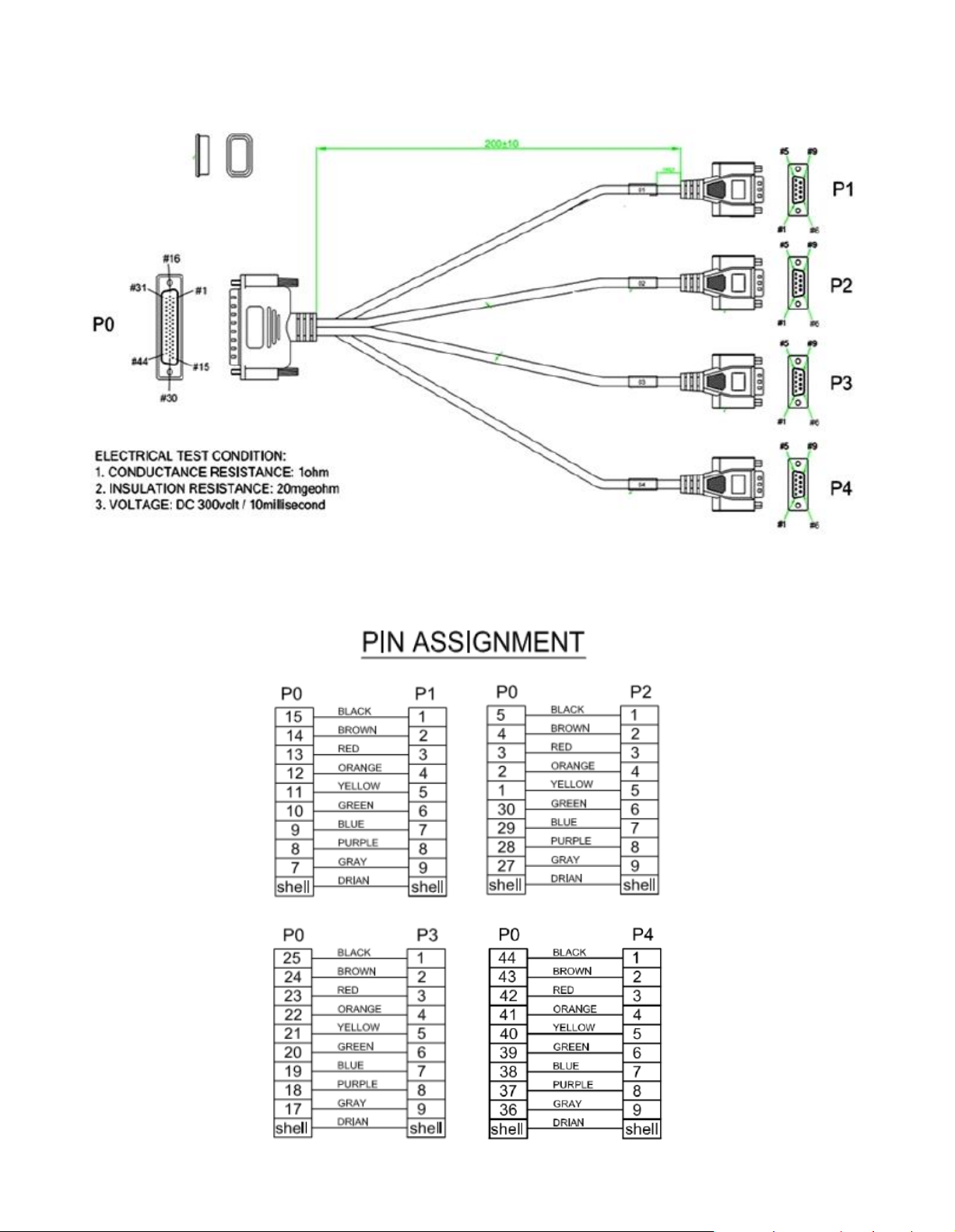
Chapter 2: Pin Definition & Jumper Settings
Pin
Signal
1
+5V
2
D-
3
D+
4
GND
Pin
Signal
1 SIM _VCC
2
SIM_ RESET
3
SIM_CLK
4
CD
5
GN D
6
Test Point
7
SIM_IO
8
COM
2-1 Front panel Pin Definition
1.
USB Connector
2. SIM Card Connector
3. Power On/Off Button
4. Rese t/ GPRS power button
5. Two system status LED
6. One GPRS power LED
7. Three GPRS speed mode LED s (LED_Type)
8. Three GPRS signal status LEDs (RSSI)
9. Five SMA Antennas for HSDPA/ GPS/ W LAN
Page 12
2-2 Rear Panel Pin Definition
1. COM 1~4 ( I/O 1 ) Connector: DB-4 4
Page 13
COM 1~4 (I/O 1) Exte rna l Cable:
Page 14
R J-45 Pin #
Def inition
RJ- 45 Pi n #
Defini tio n
1
La n_TX1+
2
La n_TX1-
3
La n_TX2+
4
Lan_TX3+
5
Lan_TX3-
6
La n_TX2-
7
La n_TX4+
8
La n_TX4-
2. DV I-D: J18 DV I 2 ( DV I-D ) c onnector
M 12 Pin #
Defini tion
M 12 Pin #
Defini tion
1
Lan_TX1+
2
Lan_TX1-
3
Lan_TX2+
4
Lan_TX3+
5
Lan_TX3-
6
Lan_TX2-
7
Lan_TX4+
8
Lan_TX4-
M12 Pi n #
Defi niti on
M 12 Pin #
D efi niti on
1
Lan_TX1+
2
Lan_T X1-
3
Lan_TX2+
4
Lan_TX3+
5
La n_T X3-
6
Lan_T X2-
7
Lan_TX4+
8
Lan_T X4-
3. DV I-I: J15 DVI 1 ( DV I-I ) c onnector
4. M icr o phone -in Connector
5. Line-Out Connector
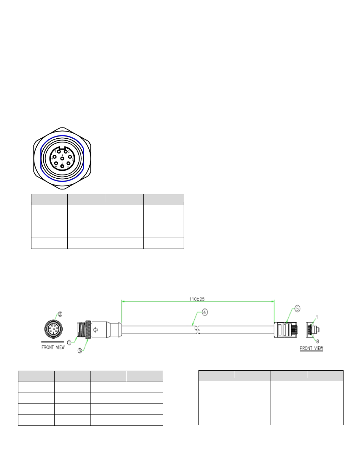
6. Female M1 2 L AN 1 ~2 Connector
Internal P IN Definition for M 12 connector, 8 -pin
7. M ale M1 2 L AN 1~2 evaluation cable (External)
Page 15
USB Pin #
Defini tion
1
USB _VCC 5
2
U SB_A-
3
USB _A+
4
GND
8. Female M1 2 U SB Conne ctor
M 12 Pin #
Defi niti on
M 12 Pin #
Definition
1
G ND
2
G ND
3
U SB_A+
4
U SB_B+
5
U SB_A-
6
USB_B-
7
U SB_VCC5
8
U SB_VCC5
M 12 Pin #
Definition
1
GND
3
U SB_A+
5
U SB_A-
7
USB _VCC 5
Internal P IN Defi ni ti on for M12 conne ctor, 8-pi n
9. Male M 12 USB evaluation cable (Exte rna l)
Page 16
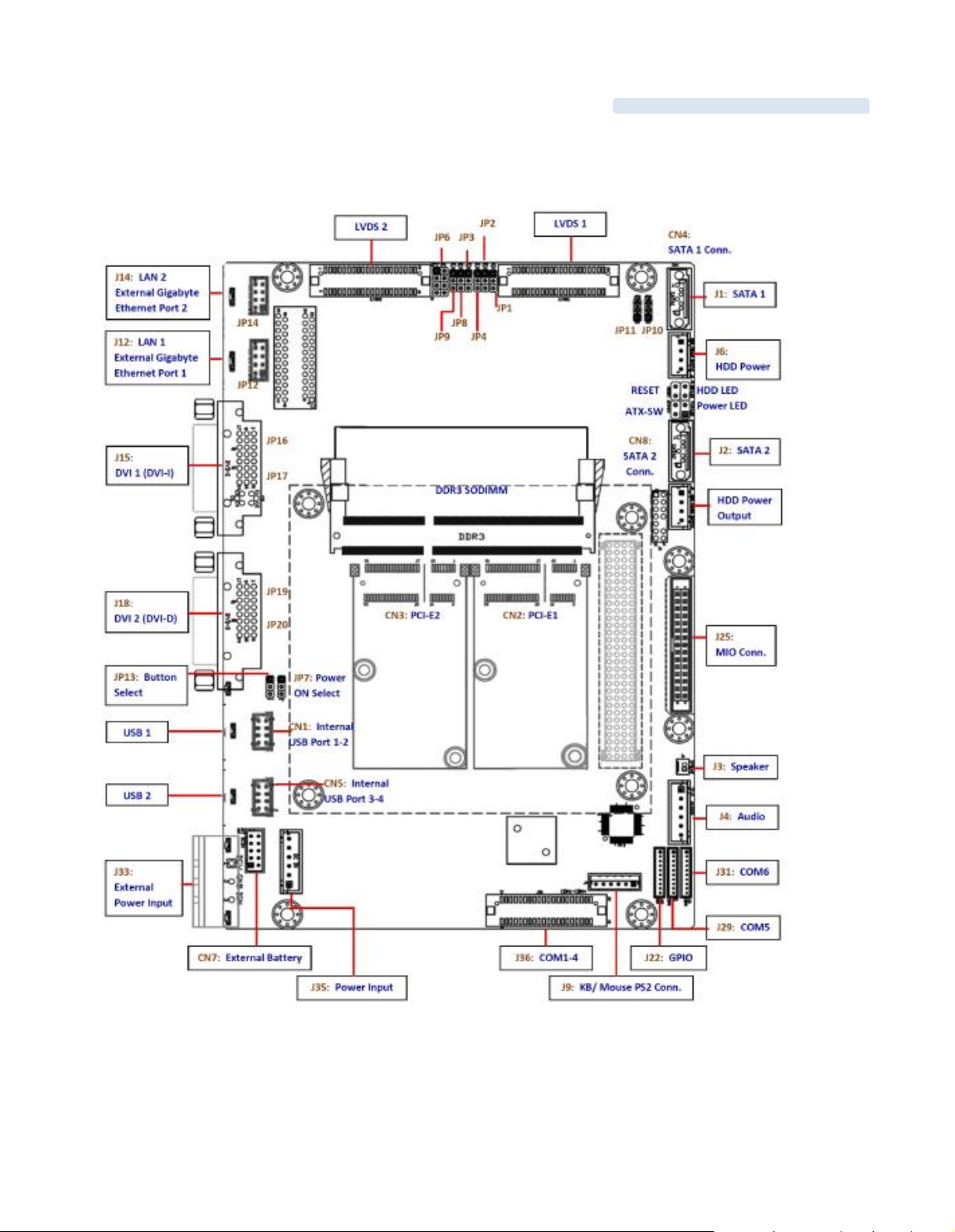
2-3 Internal
2-3. 1 Main Board Top V iew
Pin Definition & Jumper Settings
Page 17

2-3.2 Main Board P in Definition
PIN
Signal
1
+12V
2
GND
3
+5V
4
GND
PIN
Si gnal
1
GND
2
TX+
3
TX-
4
GND
5
RX-
6
RX+
7
GND
PIN
S ignal
PIN
Sign al
PIN
S ignal
PIN
Signal
1
LCDL0-
11 LCDL3+-
21 LCD_PWR
31 U SB_GND
2
LCDL0+
12
GND
22
LCD_PWR
32
U SB_DATA-
3
GND
13
DDC_DATA
23
LCD_PWR
33
U SB_DATA+
4
LCDL1-
14
DDC_CLK
24
LCD_PWR
34
U SB_VCC
5
LCDL1+
15
GND
25
GND
35
S YS-PWR-SW
6
GND
16
BL_EN/BL_E N#
26
GND
36
+12V
7
LCDL2-
17
BL_ADJ_PWM
27
BL_PWR
37
+12V
8
LCDL2+
18
GND
28
BL_PWR
38
+12V
9
GND
19
LV DS_CLK-
29
BL_PWR
39
+5V
10
LCDL3-
20
LV DS_CLK+
30
NC
40
+5V
and Jum per Settings
1. 2 .5" HDD Powe r Connector [Board Location: J1]
2. SATA Connector [Board Location: CN4 ]
3. D DR3 SODIMM
4. LV DS1 Connector [Board Location: J15 ]
Page 18

5. LVD S2 Connector [Board Location: J18]
PIN
Si gnal
PIN
Si gnal
PIN
Sign al
PIN
Si gnal
1
LC DL0-
11
LCDL3+-
21
LCD_PWR
31
U SB_GND
2
LCDL0+
12
G ND
22
LCD_PWR
32
U SB_DATA-
3
G ND
13
DD C_DATA
23
LCD_PWR
33
U SB_DATA+
4
LC DL1-
14
DD C_C LK
24
LCD_PWR
34
U SB_VCC
5
LCDL1+
15
G ND
25
GND
35
SYS -PWR-SW
6
G ND
16
B L_EN/ BL_EN#
26
GND
36
+12V
7
LC DL2-
17
B L_AD J_PWM
27
BL_PWR
37
+12V
8
LCDL2+
18
G ND
28
BL_PWR
38
+12V
9
G ND
19 LVD S_CLK-
29 BL_PWR
39
+5V
10
LC DL3-
20
LVD S_CLK+
30
NC
40
+5V
6. PCI-10 4 Slot [Board Location: CN 6]
Page 19

7. Internal KB/M ouse Connector (WTB_1X 6_2.0m m _Male_ DIP ) [Board Location: J9]
PIN
S ignal
1
M_CLK
2
+5V
3
M_DATA
4
KB_DATA
5
G ND
6
KB_C LK
Socket
Locati on
S ignal
D efault
PCI -E1
CN2
Mini PCI -E & mSATA
m SATA
PCI -E2
CN3
Mini PCI-E
PIN
Signal
PIN
S ignal
1
USB_POWER
5
USB _POWE R
2
U SB1_DATA-
6
U SB2_DATA-
3
USB1_DATA+
7
USB 2_DATA+
4
GND
8
G ND
PIN
Sig nal
1
Pow er LED+
2
Pow er LE D-
3
HD D LED+
4
HDD LE D-
PIN
Sig nal
1
PWR _BU T _IN
2
PWR_BU T_GND
3
RST_BU T_IN
4
RST_BUT _G ND
8. M ini PCI Socke t 1, 2 (Mini P CI_ 124P in_ 8mm _SMD) [Board Location: CN 2, CN 3 ]
9. External USB Port 1 ~2 [Board Location: USB1 ]
Exte rnal U SB Port 3 ~4 [Board Location: USB2]
10. Internal USB Port 1 ~2 [Board Location: CN 1]
Inte rnal U SB Port 3 ~4 [Board Location: CN 5]
11. Internal LED Conne ctor [Boa rd Location: J6]
12. Power & Reset Button Connector [Boa rd Location: J7]
Page 20

13. Internal LAN Por t 1 & LAN Port 2 Connector [B oa rd Location: J12 & J14]
PIN
Si gnal
PIN
Sig nal
1
LNA_TX1+
2
LNA_T X1-
3
LNA_TX2+
4
LNA_T X3+
5
LNA_TX3-
6
LNA_T X2-
7
LNA_TX4+-
8
LNA_T X4-
PIN
Sig nal
1
+5V
2
DI0
3
DI1
4
DI2
5
DI3
6
DI4
7
DI5
8
DO 0
9
DO 1
10
GN D
PIN
R S-232
1
D CD
2
DSR
3
RXD
4
RT S
5
TX D
6
CTS
7
DTR
8
RI
9
GN D
10
+5V
14. External DV I 1 & DVI 2 [Boa rd L ocation: J1 5 & J18 ]
15. Internal G PIO (Low Act ive) [Board Location: J2 2]
16. Internal COM5, COM6 Conne ct or [Boa rd Location: J29, J31 ]
Page 21

17. Internal COM1~ COM4 Connector [Board L ocation: J3 6]
PIN
R S-232/422/485
PIN
RS-232/422/485
1
DCD1/T XD1-/Da ta1-
2
R XD 1/ TXD1+/Data 1+
3
TXD1/RXD1+/ NA
4
DT R1/RXD1-/NA
5
G ND1/G ND1/GND1
6
DSR/RT S-/RTS1-
7
RT S1/RTS1+/RT S1+
8
CT S1/CTS1+/CTS1+
9
RI 1/ CTS1-/CTS1-
10
+5V/+5V/+5V-
11
DCD2/T XD2-/Da ta2-
12
R XD 2/ TXD2+/Data 2+
13
TXD2/ RXD 2+/NA
14
DT R2/RXD2-/NA
15
G ND2/G ND2/GND2
16
DSR2/RT S2-/R TS2-
17
RT S2/R TS2+/RT S2+
18
CT S2/CTS2+/C TS2+
19
RI 2/ CTS2-/CTS2-
20
+5V/+5V/+5V-
21
DCD3
22
RXD3
23
T XD 3
24
DTR3
25
GND 3
26
DSR3-
27
RTS3
28
CTS3
29
RI3
30
+5 V-
31
DCD4
32
RXD4
33
T XD 4
34
DTR4
35
GND 4
36
DSR4
37
RTS4
38
CTS4
39
RI4
40
+5V
PIN
Sig nal
1
LINE-OUT _R ight
2
AU DIO_AGND
3
LI NE_OUT _Left
4
LINE _I N_Right
5
MI C_IN
6
L IN E_IN _Left
18. Audio Connector [Boa rd Location: J4 ]
Page 22

19. External Power Input Connector [Board Location: J3 3]
PIN
Sig nal
1
6V~36V
2
GND
3
Ignition_IN
1
Battery_VCC
2
Ba ttery_GND
1
Buzzer-
2
Buzzer+
PIN
Si gnal
PIN
Si gnal
1
DC -IN_VCC
2
DC_IN_V CC
3
B AT_OU T_VCC
4
BAT_O UT_VCC
5
BAT_G ND
6
BAT_GND
7
BAT_G ND
8
Igni ti on_IN _TTL
9
SM _BUS_ Data
10
SM_BUS_CLK
20. B AT1: RTC Batte ry Connector
21. Optional Inte rna l Buzzer Connector [Boa rd Location: J3]
22. Optional Exte rnal Battery Conne ctor [Boa rd Location: CN7]
Page 23

D ef aul t
Jumper Selector
Po wer ON Select
1-2
Auto Power ON
x
2-3
Button POWER ON
D ef aul t
Jumper Selector
Button Sel ect
x
1-2
Pow er ON Button
2-3
System Reset Button
D ef aul t
Jumper Selector
Power IN
x
1-2
Power I n Without Control
2-3
Power I N control by Ignition or
Externa l M CU or External Ba ttery
Ignition
D ef aul t
Jumper S el ector
Igni tion Control
x
1-2
Short
Power ON Button
1-2
Open
System R eset Button
D ef aul t
Jumper Selector
CM OS
x
1-2
Short
Norm al
2-3
Short
CMOS Clea r
PIN
Si gnal
1
3.3V
2
L1_PWR
3
5V
D ef aul t
Jumper Selector
LVDS 1 Power
x
1-2
3.3V
2-3
5V
2-3.3Jum per Settings
1. Power ON Select [Boa rd Location: JP7]
2. B utton Select [Board Location: JP1 3]
3. Power IN Control Select [Board Location: JP12]
4. Ignition Select [Board Location: JP14]
5. CMOS Cle ar (Jum pe r_ 2.0mm ) [Board Location: JP5]
6. LV DS 1 Powe r Sele ct [Board Location: JP1]
Page 24

7. LV DS 1 Backlight Power Select [Board Location: JP2 ]
PIN
Si gnal
1
12V
2
BL1_PWR
3
5V
D ef aul t
Jumper Selector
LVDS 1 Backli ght Power
x
1-2
12V
2-3
5V
PIN
Si gnal
1
B L1EN
2
B L1EN_GPO
3
BL1E N#
D ef aul t
Jumper Selector
LVDS 1 Backlight Level
x
1-2
High Enable
2-3
Low Enable
PIN
Si gnal
1
3.3V
2
BL1E N_PWR
3
5V
D ef aul t
Jumper Selector
LVD S 1 B ackli ght E nabl e Power
x
1-2
3.3V
2-3
5V
PIN
Signal
1
3. 3V
2
L2_PWR
3
5V
D ef aul t
Jumper S el ector
LVDS 2 Power
x
1-2
3.3V
2-3
5V
8. LV DS 1 Backlight Enable Level Select [Board Location: JP3]
9. LV DS 1 Backlight Enable Power Select [Boa rd Location: JP4]
10. LV DS 2 Powe r Sele ct [Board Location: JP8]
Page 25

11. LV DS 2 Backlight Power Select [Board Location: JP9 ]
PIN
Signal
1
12V
2
BL2_PWR
3
5V
D ef aul t
Jumper S el ector
LVD S 2 B acklig ht Power
x
1-2
12V
2-3
5V
PIN
Signal
1
BL2EN
2
BL2E N_GPO
3
BL2EN#
D ef aul t
Jumper S el ector
LVDS 2 Backli ght Level
x
1-2
H igh Enable
2-3
Low Enable
PIN
Signal
1
3. 3V
2
BL2EN_PWR
3
5V
D ef aul t
Jumper S el ector
LVDS 2 B acklig ht Enable Power
x
1-2
3.3V
2-3
5V
D ef aul t
Jumper S elector
B utton Select
1-2
Pow er In <8V, S ys tem Keep OFF
2-3
Pow er IN <15V, System Keep OFF
5-6
Reserve d
x
7-8
Bypass This Functi on
12. LV DS 2 Backlight Enable Level Select [Board Location: JP10]
13. LV DS 2 Backlight Enable Power Select [Boa rd Location: JP11]
14. Input Power OFF Level Sele ct [Boa rd Location: J34]
Page 26

Pin
Signal
Pin
Signal
1
3 .3V SB
2
3.3VSB
3
TRST#
4
GN D
5
TDI
6
GN D
7
TM S
8
GN D
9
TCK
1 0
GN D
11
RTCK
1 2
GN D
13
TDO
1 4
GN D
15
RESET#
1 6
GN D
17
Pull down
1 8
GN D
19
Pull down
2 0
GN D
2-4
2-4.1
Power
2-4.2
GPRS
LED
Board Pin Definition & Jumper Settings
FES
GPR S
7035
Reset
G PRS B
oard Top V iew
SIM Card Socket
Board P in Definition & Jumper S etting
1 . µP JTAG (Pitch 2.0 mm [G PRS Boa rd Location: CN1 ]
LED LED LED
Page 27

2. GPRS JTAG(Pitch 2 .0 mm) [GPR S Boa rd Location: CN2 ]
Pin
Signal
Pin
Signal
1
2.6V
2
2 .6 V
3
TRST#
4
GND
5
TDI
6
GND
7
TMS
8
GND
9
TCK
10
GND
11
RTCK
12
GND
13
TDO
14
GND
15
RESET#
16
GND
17
P ul l down
18
GND
19
P ul l down
20
GND
Pin
Signal
Pin
Signal
1
M IC_P
2 3.3V
3
MIC_N
4 GND
5 SP
K_P
6
GPIO_1
7
SPK_N
8
USIM _PWR
9 GND
10
USI M_DATA
11
VC C_MSM26_DIG
12
USIM_CLK
13 NC
14
USIM _RESET
15 GND
16
GPIO_2
17 NC
18 GND
19 NC
20
W_DI SABLE#
21 GND
22
AUXV1
23 NC
24 3.3V
25 NC
26 GND
27 GND
28
GPIO_3
29 GND
30
RESERVED
31 NC
32
RESERVED
33
M DL_RESE T_N
34 GND
35 GND
36
USB_D -
37 GND
38
USB_D+
39 3.3V
40 GND
41 3.3V
42
LED_WWAN#
43 GND
44
GPIO_4
45
PC M_CLK
46
GPIO_5
47
PCM _DIN
48
GPIO_6
49
PCM_DOUT
50 GND
51
PC M_SYNC
52 3.3V
3. GSM Module Connector(Pitch 2.0 mm ) [GPRS Boa rd Location: CN8 ]
Page 28

4. GPRS/GPS Reset [GPRS Boa rd L ocation: JP3 ]
Default
Pin
Status
1-2 ( Open)
Default
1-2 ( Short)
Reset
Default
Pin
Status
1-2 ( Short)
E nable Ignition Function
2-3 ( Short)
Dis able Ig nition Function
Pin1
Pin2
Pin3
Pin4
Main Board
ON
ON
OFF
O FF
Norm al Status
(default)
O FF
OFF
ON
O N
Program ming
firm ware
SW3 .1
SW3.2
12 V
O N
O N
24 V
OFF
O N
5. Ignition Function (Pitch 2 .0 mm ) [GPRS Board Location: JP4]
6. Programming firmware (Pitch 2 .0 mm) [GPRS Board Location: SW2]
7. Select voltage input (Pitch 2.0 mm) [G PRS Boa rd Location: SW3.1 & SW3.2]
Page 29

2-4.3
Signal name
Descr
iption
Signal name
Descript
ion
A+
Data po sitive
GND
Groun d
B-
Data negative
GPI
General purp ose inp ut
CF_A
CF card ad dress
GPIO
General purp ose inpu t/ou tput
CF_CD
CF card detect
GPO
General purp ose o utput
CF_CS
CF card chip select
HDD
Har d disk
CF_D
CF card data
M B_RX
Main bo ard receiving line
CF_DMACK
DMA Acknowled ge fo r CF card D MA mode
M B_TX
Main bo ard tr ansmissio n line
CF_DMARQ
DMA request p in for CF card DMA mo de
NC
No Co nnect
CF_IORD
CF card IO read strob e
RI
Rin g detect indicator
CF_IORD Y
CF card IO ready signal
RTCK
Ret urned test clo ck outp ut
CF_IOWR
CF card IO write strobe
RTS
Req uest to send
CF_PWR
CF Power
RX
Rec eiving lin e
CF_RST
CF card reset signal
SMTCLK
I²C Clock
COM M
Commo n point
SMTDATAS
I²C Data
CTS
Clear to send
TCK
Test clock for JTAG interface
D CD
Data carrier d etect
TDI
Test d ata in for JTAG in ter face
D -IN
Digital in
TD O
Test d ata ou t for JTAG interface
D -OUT
Digital o ut
TMS
Test mod e select for JTAG inter face
D SR
Data set ready
TRST#
Test r eset fo r JTAG interface
D TR
Data terminal ready
TX
Transmission line
GP RS S
ignal Description
Page 30

Chapter 3: Software
Suppor
t Guide
3-1 Driver Installation
The GPRS m odule supports the 3G functi ons. In order to enable the function, first of all requires to install
the G PRS m odule driver onto the system of FE S 7 035 , w hi ch the appl ication at the host site can be
com municating with the GPRS de vice through the USB channel. The device driver, w hic h i s distributed by
Acnode s, has incl uded in a CD with Wi n X P or Linux revision. If running by Li nux, please build up the
kerne l system and the device dri ver. After installi ng the devi ce dri ver, user may able to exe cute the
application to com municate with the G PRS device by AT commands.
3-2
GRPS
The GP RS module com muni cates with the host, FES 7 035, vi a the UA RT port. The data confi gurations of the
UART port 6 in the host site are the baud rate 960 0, non-parity, 8-bit data byte, and 1 stop-bit.
GP RS module operates all the com mands issued by host through the UART port 6 to m onitor or control all
the functi ons that include the G PS data stream, the GP RS or GPS power On/Off functions, and the L ED
indic ator for GPRS si gnal types.
The “DEBUG _LEVEL” i s a debug flag for controll ing the level of de bug message to be displaying through the
UART port. The “DISP LAY_M SG ” is a comm and to indicate the re ceiving message for debug.
Module Softwar e Programming
i.e. When rece ivi ng the “HOST-READY” comm and from the host, the m odule wi ll feedback the data
stream of the GP S back to the host. This comm and is a toggle fl ag of the GPS and the purpose of it is to
make sure whethe r the host is ready or not. If the host is ready, the m odule wi ll se nd the data stream
to the host; if the host is not ready yet, the module wil l stop sending the stream.
Page 31

3-2.1
H eader
Command
D ata
Stop mes sag e
55
1 byte
1 byte
0D 0A
GP RS
Data Fram e Definition
Host to MC8790V command frame de finition:
<Comm and Frame Definition, all use Hex .>
Host to G PRS MCU Command and Data detail definition:
Page 32

3-2.2 Power Management C oncept
IG NITION POWER ON:
System will be directly powered ON/OFF by Ignition c ontrol
The i gniti on line signal GP I-1 at host board is a trigger of the host P ower O n signal. The l ogic “ 0” of the
input signal represents 3 vol tages, and the logi c “1 ” re presents the voltage betwee n 5V and 50V. To avoid
dam ages f rom external factors, the G PI-1 is isolated to the board via photo-coupler. The system power of
the FES 70 35 depends on the pow er signal of the G PRS m odule.
POWER BOT TON:
System will be powe red ON /OFF by user physically control
The syste m’s pow er wi ll be star ted afte r the power button being pressed and al l the conditions are ready
that include the i gnition line signal and powe r voltage ready in the GP RS m odule . Conve rsely, the system ’s
power w ill be off after the power button being pressed and hold f or 4 seconds.
Page 33

Type
Indicator
Description
Display
Netw ork
2G EDGE
3G UM TS WCDMA
3.5G
HSDP A , HSUPA
Strong
22 dBm ~ -5 8 dBm
Middle
-81 dBm ~ -70 dBm
Weak
-105dBm ~ -8 2 dBm
3-2.3
LE D
Status P rogramm ing
LED status Indicator uses the sam e GP IO de vic e driver; only w ith dif ferent I/O address, 0x2 11. The LE D
status i s connected to the GPIO-26 pin. Use the sam e driver of GPIO to execute. Data transm ission from
the GP RS module vi a USB seri al port, LED Indicator can be controll ed by the application through the serial
port via the parame ters.
LED Indica tor
Signal Strength
Page 34

3-2.4 Host to MC8790V AT
Com
mand Reference
(use Hyper Term inal S oftware)
Step 1: Use CSQ or GSTATUS AT comm and read Mobil e W ireless module M C879 0V i nformation.
Step 2 : AT c omm and GSTATUS in order to get the MC8790V inform ati on.
System M ode : WCDMA
RX level (dBm): -8 6
Page 35

Step 3: Host proc essor send UART com mand to M icro-processor, tur n on front panel G PRS_Type D7 LED.
Command name
Command
Data
D es cripti on
G PRS_T YPE 3G led on (led D7)
04
32
Connection technology : U MTS WCDM A ava ilable
Command n ame
Command
D ata
D escri ptio n
G PRS_LED_RSSI , 1 led on ( led D3)
03
30
RSSI Signal val ue , 5 ~ 16 , -105dB m ~ -82 dBm w ea k signal
Step 4: Host proc essor se nd UART com mand to M icro-processor, tur n on front panel GPRS RSSI D3 L ED.
SDK (Software D evelopm ent Kit) and concern, please contact with technical support of Acnodes for
detail confirm ation.
Page 36

Chapter 4: BIOS Set
4-1. BIOS Configuration
Over view
The m ai n board e mploys the P hoeni x Sec ureCore Ti ano BIOS. The BIOS (Basi c Input and O utput System ) is a
program used to i ni ti al ize and set up basic I/O periphe ral s of the computer, which inc ludes the P CI bus and
connected devi ces such as the diskette drive, the ke yboard and so on.
4-2. Entering BIO
Set
up
up Menu
S
When FES 7 035 is turned on, the BIO S wil l pe rf orm P ow er-O n Self Test (PO ST ) on the system and display
the size of the m emory that i s bei ng te sted. Press the [Del ] key to enter the BIOS Setup utility, and then
the m ain me nu wil l be showed on the scre en.
In this chapter we will introduce the contents of BIO S used in FES 703 5. Through understanding BIOS
se tting wi ll be helpful i n application of FES 703 5.
The BIOS Setup ma in m enu includes som e opti ons as the f oll owi ng screen. Use the
[Up/Down] arrow key to highlight the opti on that you w ant to modify, and then press the [Enter] key to
se lect the option and configure the functi ons.
System Date & S ystem T ime
In this section, you may view or re vise f or the System Date & Tim e.
Page 37

System Inform
ation
In this section, you may review for the system inform ati on clearl y.
Boot Features
1. Select Boot fe atures.
2. Selects Power-on state f or N um lock function.
Page 38

E rror
Manager
The section of Error Manager in the M ai n menu a llows for displaying error manager Log
inf orm ation.
Page 39

4-3 Advanced BIOS Features
The < Advanc ed BIOS Features> opti on consists of configuration entries that allow you to im prove the
syste m performance , or set up system features according to your prefe rence .
Quick Boot
Quick Boot is a standard feature of the SecureCore Tiano BIOS, which supports for faste st boot time
in the industry.
4-3.1 Boot Configuration
Page 40

High Resolution Graphics
Diagnostic Splash Screen
BIOS Level USB
U SB Legacy
Legacy m ode support enables devices to function in an operati ng environment that is not USBaware.
Console Redirec tion
U EFI Boot
The UEFI enables user to custom ize rapidl y, increases the com ple xity at the hardware level, and
integrates the additi onal features from the firm ware. The UEFI PO ST ti me is approxi mately 5
seconds, which satisfy user’s demand to access information instantl y.
Legacy B oot
Load OPROM
4-3.2 ACPI Configuration
This feature allows you to e nable/disabl e the Advanced Confi gurati on and P ower Management
(ACP I) .
Page 41

4-3.3 Processor Configuration
4-3.4
S
erial ATA (SAT
A)
Page 42

4-3.5 North B ridge Configuration
IG D Conf iguration
Page 43

4-3.6 South
Bridge Configuration
SB USB Configurati on
Page 44

SB PCI Expre ss Conf iguration
4-3.7 SMBIOS Event
Log
Page 45

4-3.8 Intel Fast Flash Standby
The iFFs te chnol ogy is de veloped by Intel specif ically f or SSD to al low corre ctly resum e from OS
suspensi on eve n af te r experiencing a powe r fail ure.
Page 46

4-4 Other BIOS Settings
4-4.1 Super IO Configuration
In this section, you may select the preferred Mode for appl ying onto COM1 and COM2 .
4-4.2 Hardware Monitor
This feature al lows you to m oni tor the tem perature of CP U and System temperature .
Page 47

4-5 Security Features
The SecureCore Tiano supports for TCG, iTPM , Inte l ATT and Phoe nix Fa ilSafe. It provide s a se cure root of
trust that can authe nticate operating systems, suc h as Mi crosoft Windows Vista and Windows 7. It also
provides for m ul ti -factor biometri c authentication to verify the identity of a user prior to any operating
syste m being loaded.
Features under this sec tion including:
Set or cle ar the supervisor
account’s password.
Set U ser Passw ord
A uthenti cate Use r on Boot
HDD passw ord se lectable
Set HDD U ser P assw ord
Page 48

4-6 Boot Management Setup
In this se cti on, you m ay view or conf igure devices.
Page 49

4-7 Exit BIOS Set
up
Exit Saving Changes
Thi s sele ction enables you to confirm SA VE the changes and ex it BIO S setup.
Exit Disca rding Changes
Thi s sele ction enables you to confirm Exit the BIOS setup w ithout saving any change s.
Load Setup D efaults
Thi s sele ction enables you to l oad the defa ult values for all the setup features.
Discar d Changes
Thi s sele ction enables you to discard al l the changes.
Save Changes
Thi s sele ction enables you to save all the changes been made to the BIOS setup.
Page 50

APPENDIX
GHOST
A
RE COVER Y GUIDE
1. Choose [LOCAL], which is the cate gory you going to execute re covery.
2. Choose [PARTIT ION ], w hic h is the hard-disk partiti on.
3. Choose [From Image ], which refers to recover from im age fi le.
Page 51

4. Choose the location of the image f ile where was saved.
5. Choose [3 .GH O] im age fi le as example just entered.
6. Here wil l displ ay the fi le name bei ng sel ected.
7. Cl ick on [OPEN].
Page 52

8. Check and review the Im age Fil e be ing sele cted.
9. Cl ick on [OK].
Page 53

12. Sel ect [Destination Partition], whi ch is the disk you going to recover the im age fi le FROM .
13. Af ter sel ected, cl ick [OK].
Page 54

Here is the WARNIN G to inform you the R ECOV ERY process is going to be exe cuted: Th e
info rmati on from the selected Partitio n w ill be recov ered .
14. Cli ck on [Y ES]: The recovery process wil l be gin.
Page 55

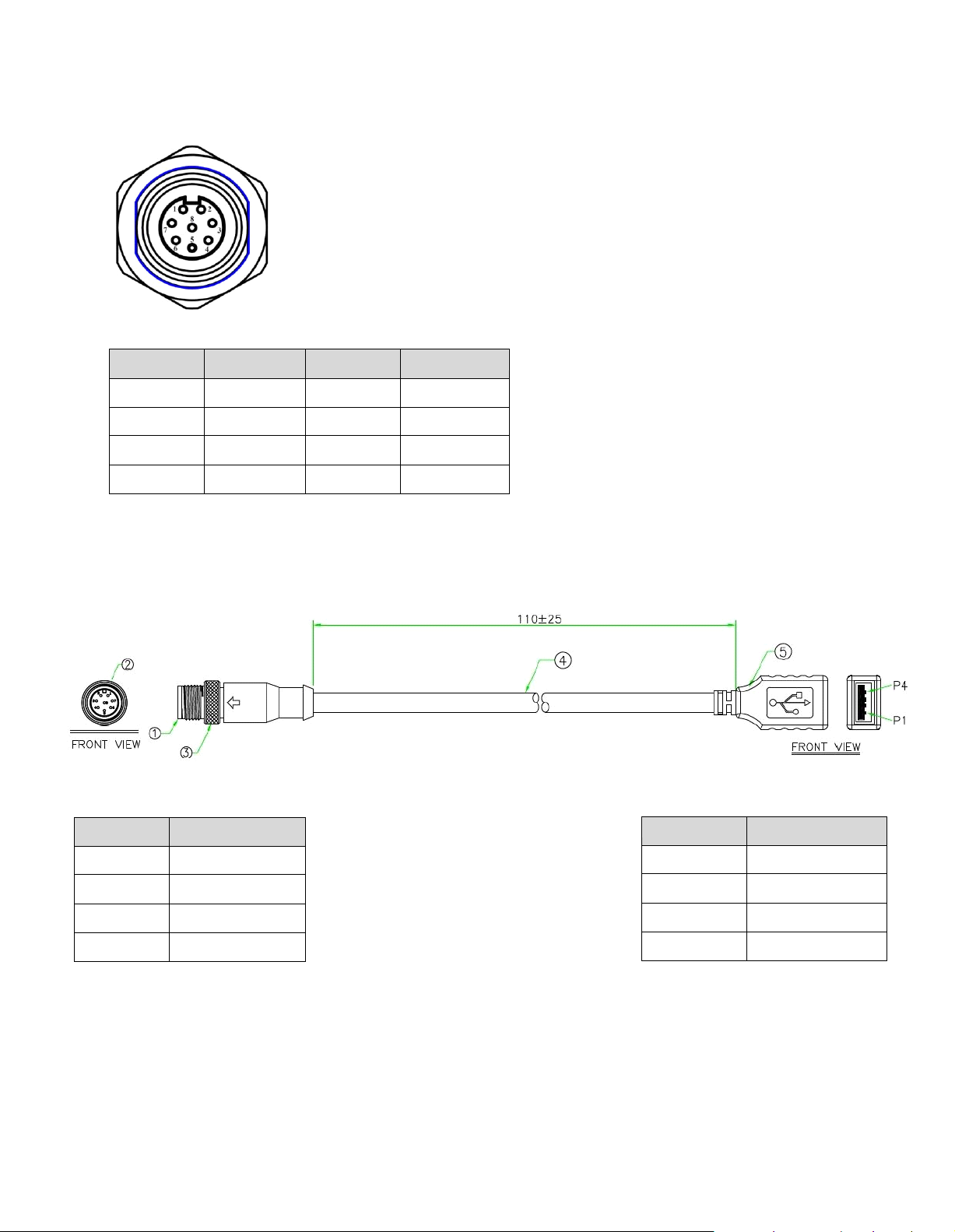
US B Pin #
Def inition
1
USB_VCC5
2
USB _A-
3
USB_A+
4
GND
A
M 12 Pin #
Defini tion
M 12 Pin #
D efi nition
1
U SB_VCC5
2
U SB_A-
3
USB _A+
4
GND
5
U SB_VCC5
6
U SB_B-
7
U SB_B+
8
GND
M12 Pi n #
D efi niti on
1
U SB_VCC5
2
USB_A-
3
U SB_A+
4
GND
PPENDIX
B
M12
USB Connector
D
efinition
Fema le M 12 LAN cable (Inter nal)
Internal P IN Definition for M 12 connector, 8 -pin
for
Lab Test
M ale M1 2 L AN evaluation cable (Exter nal)
 Loading...