

Page 1

FES2236
User Manual
FES2236: Fanless Embedded System Atom D2550
Dual Core 1.86GHz Processor
14628 Central Ave,
Chin o, CA 91710
tel: 909.597.7588, fax:909.597.1939
Fanless Embedded System
© Copyrigh t 2013 Acnodes, Inc.
All rights reserved. Product description and product specifi cations
are subj ect to chan ge without noti ce. For latest product informati on,
please visit Acnodes’ we b site at www.acnodes.c om.
Page 2

Copyright
This publi cati on c ontains inform ation that is prot ected by copyright. N o part of it m ay be reproduced i n
any form or by any m eans or used to make any transform ation/adaptation without the prior written
permission from the copyr ight holde rs. The manufacturer reserves the right to revise this publication and
m ake changes to its contents at any time, w ithout obl igation to noti fy any person or entity of such
revisions or changes.
©201 3. Al l Rights Reserved.
Trademarks
Al l tradem arks and registered trademarks of products appearing in this m anual are the properties of their
respective holders.
Notice:
1. The chan ges o r modifica tion s n ot expressly a ppro ved by th e p arty r espo nsible fo r compliance cou ld void th e user ’s auth ority
to op erate t he eq uipment .
2. Shielded int erfa ce ca bles must be used in or de r to comply wit h t he emission limits.
Static Electricity Precautions
It is quite easy to inadvertently dam age the system board, c omponents or devices e ven before i nstal ling
them i n your system unit. Static electri cal discharg e can dam age computer com ponents wi thout causing
any signs of physi cal dam age . You must take extra care in handl ing them to ensure against el ectrostatic
bui ld up.
1. To prevent electrostatic bui ld up, le ave the system board i n i ts anti-static bag unti l you are ready to install
it.
2. Wear an antistatic wrist st rap.
3. Do all preparation w ork on a stati c-free surface.
4. Hold the device only by its edges. Be careful not to touch any of the components, contac ts or
connections.
5. Avoi d touching the pins or contacting all m odul es and connectors. Hold modules or connectors by the ir
ends.
Impo rt ant:
Elect rost atic d ischa rge (ESD) can damage you r p rocessor, disk dr ive an d ot her compo nents. Perform t he up grade instru ct ion
pr ocedures describ ed at an ESD wor kstation on ly. If such a sta tion is no t availab le, yo u can provide some ESD protection by
wear in g a n ant istatic wrist st rap and attaching it to a met al part of the system chassis. If a wr ist strap is una vailab le, es tab lish
an d maintain contact with the syst em chassis th roug hout any p rocedures req uiring ESD protection .
Page 3

FES2236
Safety Measures
Fanless Embedded System
To avoid dam age to the system :
• Use the correct A C input vol tage range to reduce the risk of ele ctric shock.
• Unplug the power cord before rem oving the system chassis cover for install ati on or servi cing. After
instal lation or servicing, cover the system chassis bef ore plugging the power cord.
Batte ry:
• Dange r of expl osion if battery incorrectly replaced.
• Repl ac e only w ith the same or e quival ent type re com mend by the manufacture r.
• Dispose of used batteries according to l ocal ordinance.
Warranty
1. Warranty does not cover dam ages or fai lures caused by m isuse of the product, inabili ty to use the
product, unauthorized replacem ent or any kind of alterations of components and product
specif ications.
2. The warranty i s voided if the product has been exposed to physi cal abuse , improper instal lation, a ny
kind of modific ation, acc idents or unauthorized repair of the product.
3. Unl ess otherwise instructed in this user m anual, the user m ay not, under any ci rcum stances, attem pt to
perform servi ce , adjustm ents or repairs on the product him se lf, whether the product is sti ll covered by
warranty or not. It must be returned to the place i t was purchased at, the fa ctory or an authorized
se rvic e agency for any re pai r work.
4. We w il l not be l iabl e for any indi re ct, spe cial, incidental or conseque nt damages to the product that has
be en m odif ied or alte red.
14628 Central Ave,
Chin o, CA 91710
tel: 909.597.7588, fax:909.597.1939
© Copyrigh t 2013 Acnodes, Inc.
All rights reserved. Product description and product specifi cations
are subj ect to chan ge without noti ce. For latest product informati on,
please visit Acnodes’ we b site at www.acnodes.c om.
Page 4

FES2236
Copyright .................................................................................................................. 2
Trade marks ............................................................................................................... 2
Stati c Electrici ty P recautions .................................................................................... 2
Safety Me asures ....................................................................................................... 3
Warranty ................................................................................................................... 3
Chapter 1: Introduction
1-1 O verview .............................................................................................................. 5
1-2 P roduct Specification........................................................................................... 6
1-3 System Block Di agram ....................................................................................... .. 8
1-4 Me chanical Diagram ........................................................................................... 9
1-5 Front & Rear I/O ………........................................................................................... 10
Chapter 2: Pin D efinition & Jumper Se ttings
2-1 2 236U Fr ont panel P in Defi ni ti on……………….…………………………………………………… 11
2-2 2 236U Rear panel Pin Definition……… ……………………………………… ……………………… 13
2-3 Internal P in Defi niti on & Jum per Settings…………………………………………….…………. 16
2-4 MIO Board P in Definition & Jumper Settings…………………………………………………… 26
Chapter 3: BIOS Setup Menu
3-1 BIOS Configuration O verview ………………………………………… ………………………………. 30
3-2 Entering BIO S Setup……… …………………………………………………… …………………………… 30
3-3 Advanced BIOS Fe atures…………………………… ……………………………………………………. 33
3-4 O ther BIO S Settings ……..……………… …………………………………………………… …… ….….. 40
3-5 Security Feature s…..………………… ……………………………………………… …… ..……………... 41
3-6 Boot M anagem ent Setup………………..……………………………………… …………….……..…. 42
3-7 Exi t BIO S Setup………… ………………..… ……………………………………………… ………………... 4 3
Appe ndix A..…………………… ……… ………………………………………………………… …… …… ……… 44
14628 Central Ave,
Chin o, CA 91710
tel: 909.597.7588, fax:909.597.1939
Fanless Embedded System
Table of Con tents
© Copyrigh t 2013 Acnodes, Inc.
All ri ghts reserved . Produ ct descri pti on an d produ ct specificati ons
are subj ect to chan ge without noti ce. For latest product informati on,
please visit Acnodes’ we b site at www.acnodes.c om.
Page 5

FES2236
Chapter 1: Intr
1-1 Overview
oduction
Fanless Embedded System
Acnodes’ FE S 22 36 supports the exclusi ve features to provi de custom er an improved and outstandi ng
experie nce by applying the Atom D2550 processor, ( N28 00/ N2 600 avai labl e based on custom ers’ choic e)
w ith its outstanding and re liable embedded system with hi gh performance and low pow er consum ption
rema ined.
The ne w launched Atom ™ P rocessor D25 50 Dual-core 1.86 GHz Processor carries out an enhanced function in
graphic performance for increasi ng the capabil ity in multi-media. The new FES2 236 supports for reaching up
to 4 GB DDR3 - 8 00/1 066 as its maxim um me mory. For the disk dri ve storage, it is desi gned with 2.5” SATA
HDD and one M ini -P CI-E m SATA.
In orde r to m eet the network stabil ity, FES 2 236 uses two Realtek 81xx 100 /10 00 Mbps LA N w ith
Wake-On L AN & DM I to support and m aintain Ethe rnet function. The system designed w ith tw o D B-9
supports for RS-23 2/ 422/ 485 and two for RS-2 32 interface with auto-flow control; the expansion
avail abi lity could be up to si x COM s by re quest. It also provides a software program mi ng Watchdog (WDT)
with tim er range from 1 to 25 5 seconds. For the audio output, the re has occupied wi th an ALC 66 2 for
spe aker.
In displ ay function, it supports for dual displ ay of DVI-I+DVI-D, and the VGA supports for 1920 x 1 200
(1 080P ) resol utions. FES 2 236 is equipped by NM1 0 South Bridge Chipset that suppli es high speed storage
interface as i n faste r data transfer rate. For ex tended I/O devices, there i s an optional support for 8 bit GP IO
w ith T TL level provided.
FES 223 6 is capable to accept DC power i nput from 6 V~34 V. The power consumption can reach up to
22W in m ax imum with D25 50 chipsets. The syste m also offe rs optional support for A nti-Vibration and
Anti-Shock functiona lities to enhance the perform ance and durability of FES 223 6. The system is
valuable for all the em bedded applicati ons, and also we ll support with the Wi ndow 7, Window s XP and
Linux Operation system.
14628 Central Ave,
Chin o, CA 91710
tel: 909.597.7588, fax:909.597.1939
© Copyrigh t 2013 Acnodes, Inc.
All rights reserved. Product description and product specifi cations
are subj ect to chan ge without noti ce. For latest product informati on,
please visit Acnodes’ we b site at www.acnodes.c om.
Page 6

1-2 Pr
oduct Specification
P
rocessor
At om D25 50 D ual-core 1.86 GHz Pr ocessor
At om N2800 Dual-co re 1. 86 GHz Pro cesso r
At om N2600 Dual-co re 1. 6 GHz Processor
Chipset
NM 10 south Bridge C hipset
S
ystem Mem
1 SODIMM Socket, up to 4 GB 800/ 1066 MHz D DR3 Memory
E
xpansion S lots
1 P CI-104 expansion nod ule (2PCI master)
2 M ini-PC I-E expansion slo t
Graphics
Gr ap hic cor e 640 Mhz (D2550/N2800)/ 400 Mhz (N2600)
Sup por t AVC/ H.264, VC1/WMV9, MPEG2 HW engin e
Blu -Ray sup port (D2550)
HD CP 1.3 an s PAVP 1. 1C content pr otectio n su pport
Sup por t M icro soft DXVA 2.0 an d Overlay D D
MS C OPP and P VP -OPM supp ort
Enabling key ISVs-Cor el, Cyberlink, ArcSo ft
Sup por ts OpenGL 3.0 and Micro soft DirectX9
Display
Sup por t D VI-I+DVI-D or Dual 18/24 b it LVDS du al display
DVI, VGA sup port 1920 x 1200 (1080 p) resolution
D2550 LVDS sup port 1 channel 2 4 bit 1440 x 900 resol utio n
N2 800/ N2600 LVDS supp or t 1 ch an nel 24 bit 1366 x 7 68 resolution
Audio
AL C 662 HD Co dex su ppo rt
BIOS
Pho en ix BIOs, Supp or t P ower On After Power Failu re
E
thernet
2 Realtek 81x x 100/1 000 M bps L AN with Wake-On LAN & DM I
Disk Drive Storage
2.5” SATA HDD (occup y 1 PCI-104 sp ace)
mSATA (occup y 1 Mini-P CI -E)
RS -
232/422/485 S
2 DB-9 for RS-232/422/485 & 2 for RS-232 (rear COM 1) with aut o-flow co ntrol.
W atchdog T im er
Programmab
Function
le WDT from 1 to 255 second s/ minu tes
ory
upport
Page 7

Optional
Optional sup port 8 bit GPIO with TTL level
Remote Power
Option al sup port Remote Power On /Off function
support Digital I/O
On
Front P
Power & HDD LED, Power & System Reset button
2 USB, 4 DB-9 for RS-232,
anel Extend I/O
Removab
le CF
Rear Panel Extend I/O
Scr ew-Lock DC p ower in put conn ec tor
1 female DB-44 (COM 2) to 4 male DB-9 fo r 2 RS-232/422/485 &2 RS-232
DVI-I + DVI-D disp lay int erface
4 USB, 2 RJ-45 100/100 0 Mb it LAN connector
1 Mic ro pho ne-in , 1 Line-o ut con nector (o ccupy D B-44 I/O 1 space; may remove Micro Phone-in & Line-o ut fo r o ptio nal
I/O exp ansio
Rear Panel Optional I/O
2 DB-9/15 (C OM 3 & 4) for PCI -104 module or COM 5, 6
P
ower S upply
DC 6V~34V in put, 24 VDC/0.85A, 12VDC/ 1. 7A, AT/ATX po wer type
Power ad ap ter : AC to DC , D C 12V/5A 60W (Optional)
P
ower
Typical P ower Co nsu mpt io n: 17W/ 12W/ 9W (D2550 / N2800/ N2600)
Maximum Power C onsumption: 22W/ 17 W/ 14W (D 2550/ N2800/ N26 00)
E nvironment
Operatio
- With extend temperature HDD :
- With SSD / mSATA:
Stor age Temperature:
Relative Humidity: 10%~90%
An ti-Vibration (o peration):
-
MIL-810F-514.5C -VII
- 2G rms @10~500Hz r an dom, 3 axes (HD D with anti-vib ration kit, SSD /mSATA withou t anti-vibration kit)
An ti-Shoc k (n on-operation):
-
IEC-60028-2-27
- 50G rms, 11ms dur atio n (HD D with an ti-vib ration kit, SSD / mSATA with out anti-vib ratio n kit)
Dim ensions and Weight
Dimen sion W x H x D: 200mm x 89.83mm x 185.5mm (7. 87” x 5.34” x 7.30”)
Weight (Net/ Gross): 4.2 KG (9.24lb)/ 4.8KG (10.56lb)
Mechanical
Mou nting: D esk/ Wall Mou nt
Con stru ction: Aluminum h ousing
Certification &
CE/FCC C lass A
n).
Consum ption (with
n Temperature:
-20°C~60°C
-40°C~85°C
(Non-con
OS Supports
HDD )
-20°C~60°C
densin g)
Page 8
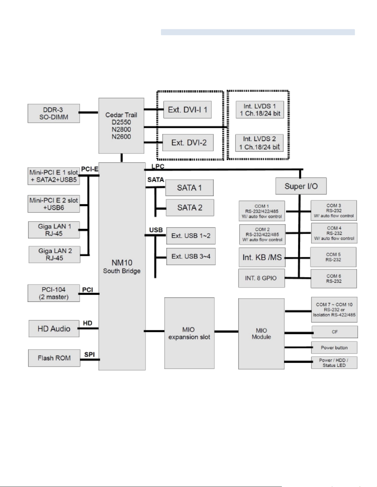
1-3 System
FES
2236
Block Diagram
Page 9
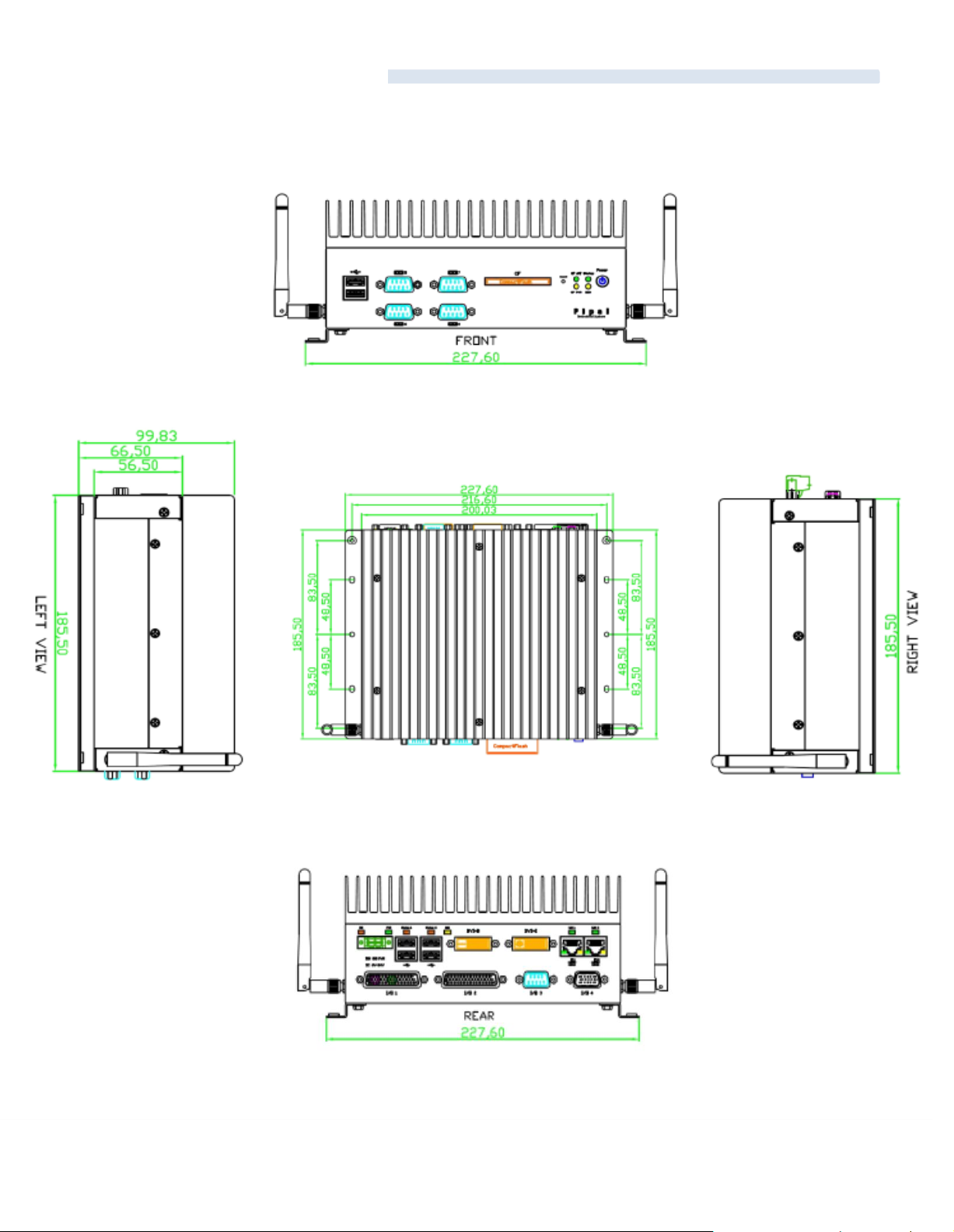
1-4 Mechanical Diagram
FES
2236
s
Page 10
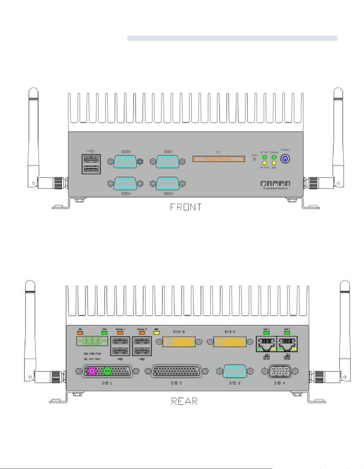
1-5 Front & Rear I/O
Front
Panel
Rear Panel
Page 11
Chapter 2: Pin Definition
PIN
Sig nal
PIN
Sig nal
1
5V 5 5V
2
D- 6 D-
3
D+ 7 D+
4
G ND
8
GND
PIN
Sign al
PIN
Si gnal
1
DCD
6
C TS
2
DSR
7
D TR
3
RXD
8
RI
4
RTS
9
GND
5
TXD
10
+5V
2-1 2236 Front panel Pin Definition
1.
Two U SB Connector
2.
Power On/Off Button
3.
System Reset B utton
4.
Power, HDD L ED
& Jumper Settings
5. COM 5-8 (D B-9): RS-232
Page 12

6.
Pin
Definition
Pin
D efi niti on
1
G ND
26
NC
2
C F_D3
27
CF _D11
3
C F_D4
28
CF _D12
4
C F_D5
29
CF _D13
5
C F_D6
30
CF _D14
6
C F_D7
31
CF _D15
7
CF_CS0
32
CF_CS1
8
G ND
33
NC
9
G ND
34
C F_I ORD
10
G ND
35
C F_I OWR
11
G ND
36
CF_PWR
12
G ND
37
NC
13
C F_PWR
38
CF_PWR
14
G ND
39
Ca ble Select
15
G ND
40
NC
16
G ND
41
CF_RST
17
G ND
42
CF_IORDY
18
CF_A2
43
C F_DMARQ
19
CF_A1
44
C F_DMACK
20
CF_A0
45
NC
21
C F_D0
46
NC
22
C F_D1
47
CF_D8
23
C F_D2
48
CF_D9
24
NC
49
CF _D10
25
C F_C D
50
GN D
Signal name
Descr
iption
Signal name
Description
D
+
Data p
ositive
RTS
Requ est To
Send
D
-
Data
negative
TXD
Tr an smitted Data
GND
Grou
nd
CTS
Clear To
Send
DC
D
Data Carrier D etec t
DTR
Data Termin al Ready
DSR
Data Set Ready
RI
Ring Ind
icator
RX
D Rec eived D
ata
CF Socke t
Page 13
2-2 2236 Rear panel Pin Definition
PIN
Definition
PIN
D efi niti on
1
LINE_OUT _Left
2
LI NE_OUT _Rig ht
3
AU DIO_AGND
4
AUDI O_AGND
5
LINE_IN_Left
6
LINE_IN_Rig ht
7
AU DIO_AGND
8
AUDI O_AGND
9
Mi cro phone_I N1
10
M icro phone _I N2
PIN
Definition
PIN
D efi niti on
1
Lan_T X1+
2
Lan_T X1-
3
Lan_T X2+
4
Lan_TX3+
5
Lan_TX3-
6
Lan_T X2-
7
Lan_T X4+
8
Lan_T X4-
PIN
Definition
1
90V-120V
2 G ND
3
Remote On/Off
PIN
Sign al
PIN
Si gnal
1
DCD
6
C TS
2
DSR
7
D TR
3
RXD
8
RI
4
RTS
9
GND
5
TXD
10
+5V
1. Micro phone-out Connector
2. Line-Out Connector
3. LAN 1 & 2 (RJ-45)
4. DVI-D: J1 8 DV I 2 ( DVI-D ) connector
5. DVI-I: J15 DV I 1 ( DVI-I ) connector
6. Power Input
7. COM 3 & 4 (DB -9/ DB-15): Optional PCI-104 extension module
8. COM 1 (D B-9): RS-232
Page 14
9.
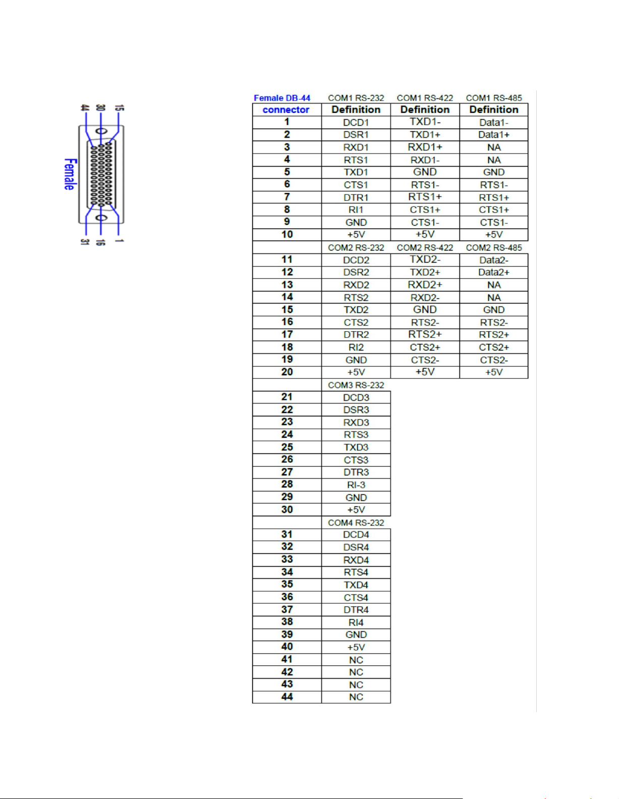
COM 2 Connector (DB-44 ): RS-23 2/ 42 2/ 4 85
Page 15
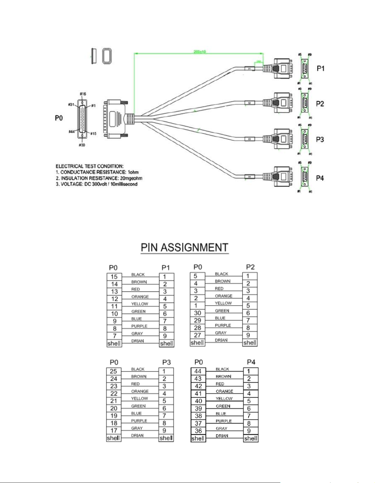
COM 2 Exter nal Cable:
Page 16

2-3 Internal
2-3.1 Main B oard Top View
Pin Definition & Jumper Settings
Page 17

2-3.2 Main Board Pin Definition
PIN
Sig nal
1
+12V
2
GND
3
+5V
4
GND
PIN
S ignal
1
G ND
2
TX+
3
TX-
4
G ND
5
RX-
6
R X+
7
G ND
PIN
Si gnal
PIN
Sig nal
PIN
Sig nal
PIN
S ignal
1
LC DL0-
11
LCD L3+-
21
LCD _PWR
31
U SB_G ND
2
LC DL0+
12
GND
22
LCD _PWR
32
U SB_D ATA-
3
GND
13
DDC_DATA
23
LCD _PWR
33
U SB_D ATA+
4
LC DL1-
14
DDC_CLK
24
LCD _PWR
34
U SB_VCC
5
LC DL1+
15
GND
25
GND
35
SYS-PWR-SW
6
GND
16
BL_E N/BL_EN#
26
GND
36
+12V
7
LC DL2-
17
BL_ADJ_PWM
27
BL_PWR
37
+12V
8
LC DL2+
18
GND
28
BL_PWR
38
+12V
9
GND
19
LVDS_CLK-
29
BL_PWR
39
+5V
10
LC DL3-
20
LVDS_CLK+
30
NC
40
+5V
1. 2 .5" HDD Power Connector [Board Location: J1]
and Jum per S ettings
2. SATA Connector [Board Location: CN4]
3. D DR3 SODIMM
4. LV DS1 Connector [Board Location: J15]
Page 18

5. LVD S2 Connector [Boa rd Location: J18 ]
PIN
Si gnal
PIN
Si gnal
PIN
Si gnal
PIN
Sig nal
1
LCDL0-
11
LCDL3+-
21
LCD_PWR
31
USB_GND
2
LCDL0+
12
GND
22
LCD_PWR
32
USB_DATA-
3
GND
13
DDC_D AT A
23
LCD_PWR
33
USB_DATA+
4
LCDL1-
14
DDC_C LK
24
LCD_PWR
34
USB_VCC
5
LCDL1+
15
GND
25
GND
35
SYS-PWR-SW
6
GND
16
BL_EN/BL_EN#
26
GND
36
+12V
7
LCDL2-
17
BL_AD J_PWM
27
BL_PWR
37
+12V
8
LCDL2+
18
GND
28
BL_PWR
38
+12V
9
GND
19
LVD S_CLK-
29
BL_PWR
39
+5V
10
LCDL3-
20
LVD S_CLK+
30
NC
40
+5V
6. PCI-10 4 Slot [Board Location: CN6 ]
Page 19

7. Internal KB/M ouse Connector ( WTB_1 X6_ 2.0mm _M al e_DIP) [B oard Location: J9]
PIN
Sign al
1
M_CLK
2
+5V
3
M_DATA
4
KB_DATA
5
G ND
6
KB_CLK
Socket
Location
Sig nal
Defaul t
PCI -E1
C N2
M ini PCI-E & m SATA
m SATA
PCI -E2
C N3
Mini PCI- E
PIN
S ignal
PIN
Sig nal
1 U SB_POWER
5 U SB_POWER
2
USB1_DAT A-
6
U SB2_DATA-
3
U SB1_DATA+
7
U SB2_DATA+
4
G ND
8
GND
PIN
Signal
1
Power LED+
2
Pow er LED -
3
HDD LED+
4
H DD LE D-
PIN
Signal
1
PWR_BU T_IN
2
PWR_BUT_GND
3
RST_BU T_IN
4
R ST_BUT _G ND
8. Mini PCI Socket 1, 2 (Mini PCI_124P in_8m m_SMD) [Boa rd Location: CN 2, CN 3]
9. External USB Por t 1~2 [B oa rd Location: USB1]
External USB Port 3~4 [Board Location: USB2]
10. Internal USB Por t 1~2 [Board Location: CN1]
Internal U SB Port 3~4 [Board Location: CN5]
11. Internal LED Connector [Board Location: J6]
12. Power & Reset Button Connector [Board Location: J7]
Page 20

13 . External L G igabyte Ether ne t Port 1 & Port 2 [Board Location: J11 & J13]
PIN
Sig nal
PIN
S ignal
1
LNA_TX1+
2
LNA_TX1-
3
LNA_TX2+
4
LNA_TX3+
5
LNA_TX3-
6
LNA_TX2-
7
LNA_TX4+-
8
LNA_TX4-
PIN
Sig nal
1
+5V
2
DI 0
3
DI 1
4
DI 2
5
DI3
6
DI4
7
DI5
8
DO 0
9
DO 1
10
GND
PIN
RS-232
1
DCD
2
DSR
3
RXD
4
R TS
5
TXD
6
CTS
7
DTR
8
RI
9
GND
10
+5V
Internal LAN Port 1 & L AN Port 2 Connector [B oard Location: J1 2 &J14]
14 . External DV I 1 & DV I 2 [Board Location: J15 & J18 ]
15 . Internal GPIO (Low Active) [Boa rd Location: J2 2]
16 . Internal COM 5, COM 6 Connector [Board Location: J29, J31 ]
Page 21

17 . Internal COM 1~COM4 Conne ctor [Boa rd Location: J3 6]
PIN
RS -232/422/485
PIN
R S-232/422/485
1
D CD1/ TXD1-/ Data 1-
2
R XD 1/T XD 1+/Data1+
3
TXD1/RXD1+/NA
4
D TR1/RXD1-/NA
5
GND1/GND1/GND 1
6
DSR/RT S-/RTS1-
7
RT S1/ RTS1+/ RTS1+
8
CT S1/ CTS1+/ CTS1+
9
RI1/CT S1-/ CTS1-
10
+5V/+5V/+5V-
11
D CD2/ TXD2-/ Data 2-
12
R XD 2/T XD 2+/Data2+
13
TXD2/RXD2+/NA
14
D TR2/RXD2-/NA
15
GND2/GND2/GND 2
16
DSR2/RTS2-/RT S2-
17
RT S2/ RTS2+/ RTS2+
18
CT S2/ CTS2+/ CTS2+
19
RI2/CT S2-/ CTS2-
20
+5V/+5V/+5V-
21
DC D3
22
RX D3
23
TXD3
24
DTR3
25
G ND3
26
DSR3-
27
RT S3
28
CTS3
29
R I3
30
+5V-
31
DC D4
32
RX D4
33
TXD4
34
DTR4
35
G ND4
36
DSR4
37
RT S4
38
CTS4
39
R I4
40
+5V
PIN
Sig nal
1
LINE-OU T_Right
2
AUDI O_AG ND
3
LI NE _OU T_Left
4
LINE_IN_Right
5
M IC_IN
6
LINE_IN_Left
PIN
Sig nal
1
6V~36V
2
GND
3
Ig ni tion_I N
18 . Audio Conne ctor [Board Location: J4 ]
19 . External Power Input Connector [Board Location: J3 3]
Page 22

20 . BAT 1: RTC Battery Connec tor
1
Battery_VCC
2
Ba ttery_G ND
1
Buz zer-
2
Buzz er+
PIN
Sig nal
PIN
Sig nal
1
DC -IN _VCC
2
DC_ IN _VCC
3
BAT_OU T_VCC
4
BAT_ OUT_VCC
5
BAT_GN D
6
BAT_GN D
7
BAT_GN D
8
Ignition_IN_TTL
9
SM_ BU S_ Data
10
SM_ BU S_CLK
21 . Optional Internal Buzzer Conne ctor [Board Location: J3 ]
22 . Optional External Battery Connector [Board Location: CN7]
Page 23

2-3.3Jumper Settings
Def aul t
Jumper Selector
Power ON S elect
1-2
Auto Pow er ON
x
2-3
B utton POWER ON
Def aul t
Jumper Selector
B utton Select
x
1-2
Power ON B utton
2-3
Sys tem Reset Button
Def aul t
Jumper Selector
Po wer IN
x
1-2
Power I n Wi thout Control
2-3
Power I N control by I gnition or
External MCU o r Externa l Battery
Ig nition
Def aul t
J umper Sel ecto r
Ignition Control
x
1-2
Sho rt
Power ON Button
1-2
Open
Sys tem Reset Button
Def aul t
J umper Sel ecto r
CMOS
x
1-2
Short
Norm al
2-3
Short
CM OS Cl ear
PIN
Si gnal
1
3. 3V
2
L1_PWR
3
5V
Def aul t
Jumper Selector
LVD S 1 Power
x
1-2
3. 3V
2-3
5V
1. Power ON Select [Board Location: JP7]
2. Button Se lect [Board Location: JP13]
3. Power IN Control Select [Board Location: JP12 ]
4. Ignition Select [Board Location: JP14 ]
5. CM OS Cle ar ( Jumper_2.0m m) [Board Location: JP5]
6. LV DS 1 Powe r Select [Boa rd Location: JP1 ]
Page 24

7. LV DS 1 Backlight Powe r Select [Boa rd Location: JP2]
PIN
Si gnal
1
12V
2
BL1_PWR
3
5V
Def aul t
Jumper Selector
LVDS 1 Backlight Power
x
1-2
12V
2-3
5V
PIN
Si gnal
1
BL1EN
2
BL1EN_G PO
3
B L1EN#
Def aul t
Jumper Selector
LVD S 1 B ackli ght Level
x
1-2 High E nable
2-3
Low Ena ble
PIN
Si gnal
1
3. 3V
2
B L1EN_PWR
3
5V
Def aul t
Jumper Selector
LVDS 1 Back light Enable Po wer
x
1-2
3. 3V
2-3
5V
PIN
Sig nal
1
3. 3V
2
L2_PWR
3
5V
Def aul t
J umper Sel ecto r
LVDS 2 Power
x
1-2
3.3V
2-3
5V
8. LV DS 1 Backlight Enable Level Select [Boa rd Location: JP3 ]
9. LV DS 1 Backlight Enable Power Select [Board Location: JP4]
10.
11. LV DS 2 Powe r Select [Boa rd Location: JP8 ]
Page 25

12. LV DS 2 Backlight Powe r Select [Boa rd Location: JP9]
PIN
Sig nal
1
12V
2
B L2_PWR
3
5V
Def aul t
J umper Sel ecto r
LVDS 2 Backl ight Power
x
1-2
12V
2-3
5V
PIN
Sig nal
1
BL2E N
2
BL2E N_GPO
3
BL2E N#
Def aul t
J umper Sel ecto r
LVDS 2 B ackligh t Level
x
1-2
High Ena ble
2-3
Low Ena ble
PIN
Sig nal
1
3. 3V
2
BL2EN_PWR
3
5V
Def aul t
J umper Sel ecto r
LVD S 2 Backli ght Enabl e Power
x
1-2
3.3V
2-3
5V
Def aul t
J umper Sel ector
Button Sel ect
1-2
Pow er In <8V, System Keep OFF
2-3
Pow er IN <15V, System Keep OFF
5-6
Reserved
x
7-8
Bypass This Function
13. LV DS 2 Backlight Enable Level Select [Board Location: JP10 ]
14. LV DS 2 Backlight Enable Power Select [Board Location: JP11]
15. Input Power OFF Level Select [Board Location: J34]
Page 26

2-4 MIO Board Pin Definition & Jumper Settings
PIN
Signal
1
5V
2
D-
3
D+
4
G ND
PIN
Sig nal
PIN
Sign al
1
V CC3
2
VC C3
3
TR ST#
4
GND
5
T DI
6
GND
7
T MS
8
GND
9
TC K
10
GND
11
RTCK
12
GND
13
TDO
14
GND
15
RE SET#
16
GND
17
Pull dow n
18
GND
19
Pull dow n
20
GND
2-4.1
2-4.2 MIO
1. USB Connector [MIO Board Location: CN1 ]
FES
2236 MIO
B
oard Pin D efinition
Board Top View
2. uP JTAG [MIO Board Loc ation: CN3]
Page 27

3. CF Socket [M IO Board Location: CN 4]
PIN S ignal
PIN Si gnal
1
GND
26
NC
2
CF_D3
27
C F_D11
3
CF_D4
28
C F_D12
4
CF_D5
29
C F_D13
5
CF_D6
30
C F_D14
6
CF_D7
31
C F_D15
7
C F_CS0
32
CF_CS1
8
GND
33
NC
9
GND
34
CF_I OR D
10
GND
35
C F_I OWR
11
GND
36
CF_PWR
12
GND
37
NC
13
C F_PWR
38
CF_PWR
14
GND
39
Ca ble Select
15
GND
40
NC
16
GND
41
CF_RST
17
GND
42
CF_IORDY
18
CF_A2
43
C F_DM ARQ
19
CF_A1
44
CF_DMACK
20
CF_A0
45
NC
21
CF_D0
46
NC
22
CF_D1
47
CF_D 8
23
CF_D2
48
CF_D 9
24
NC
49
C F_D10
25
CF_CD
50
GND
PIN
S ignal
PIN
Si gnal
1
DCD
6
DSR
2
RXD
7
RTS
3
TXD
8
CTS
4
DTR
9
RI/ 5V
5
GND
4. RS-232 Connector [MIO Board Location: CN5(A,B)]
Page 28

5. RS-232 Connector [MIO Board Location: CN6(A,B)]
PIN
Signal
PIN
Si gnal
1
DC D
6
DSR
2
RXD
7
RTS
3
T XD
8
CTS
4
DT R
9
RI
5
G ND
PIN
Signal
PIN
Si gnal
1
NC
2
DSR2-
3
RX
4
RT S2-
5
T X
6
C TS2-
7
DTR2-
8
NC
9
G ND
10
NC
PIN
Signal
PIN
Si gnal
1
5V 5 5V
2
D- 6 D -
3
D + 7 D+
4
G ND
8
GND
RS-23 2
6. COM Port Conne ct or [M IO Boa rd Location: COM 1]
7. USB Connec tor [M IO Board Location: USB2]
Page 29

2-4.3 MIO
B
oard Jumper S etting
1. uP Programming (P rogrammer Interface Connected to COM 1) [MIO Board Location: JP1]
2. CF Select [M IO Board Location: JP2]
3. Supply 5V [CN5 (A,B)Pin 9] [MIO Board Location: JP3 & JP4]
4. Power ON Mode Select [M IO Board Location: JP5 & JP6]
Page 30

Chapter 3: BIOS Setup Menu
3-1. BIOS Configuration Overview
The m ain board em ploys the P hoenix SecureCore Tiano BIOS. The BIOS (Basic Input and O utput System ) is a
program used to i ni ti alize and set up basic I/O periphe rals of the compute r, which includes the P CI bus and
connec ted devices such as the di skette drive , the keyboard and so on.
3-2. Entering BIOS Setup
When FES 2 236 i s turned on, the BIO S wi ll perform Powe r-O n Self Te st ( PO ST) on the system and
display the size of the mem ory that i s being tested. P re ss the [Del] ke y to ente r the BIOS Setup utility, and
then the main m enu wi ll be show ed on the screen.
In thi s chapter w e wil l i ntroduce the contents of BIO S used in FES 22 36 . Through understanding BIO S
se tting wi ll be helpful in applicati on of FES 2 236 .
The BIO S Setup m ain menu include s some opti ons as the following screen. Use the
[Up/Down] arrow key to highlight the option that you want to m odify, and then pre ss the [Enter] key to
se lect the option and confi gure the functions.
S
ystem D ate & System
In thi s secti on, you m ay view or revise for the System Date & Time.
Tim e
Page 31

S
ystem Inform ation
In this section, you may review for the system inf orm ation clearly.
B oot Features
1. Select Boot f eatures.
2. Selects Power-on state for Numl ock funct ion.
Page 32

E rror M
anager
The sec ti on of Error Manage r in the Main me nu all ows f or displayi ng er ror m anager Log
inf orm ation.
Page 33

3-3 Advanced BIOS Features
The <Advanced BIO S Feature s> option c onsi sts of conf iguration entri es that al low you to improve the
syste m performance, or set up system features accordi ng to your pre ference.
3-3.1 Boot Configuration
Quick B oot
Quick Boot is a standard feature of the Secure Core Tiano BIOS, whi ch supports f or f astest boot time
in the industry.
Page 34

High Resolution Graphics
Diagnostic Splash Screen
BIOS Level USB
U SB Legacy
Legacy m ode support enable s devices to funct ion in an operat ing environm ent that is not
USB-aware.
Console Redire ction
U EFI Boot
The UEFI ena ble s user to customize rapidly, inc reases the complexi ty at the hardware level, and
integrates the additional features from the fi rm w are . The UEFI P OST tim e is approxi mately 5
seconds, whic h satisfy user’s dem and to access information i nstantl y.
Legacy Boot
Load OPROM
3-3.2
ACP I Configuration
Thi s feature allows you to e nable/di sable the Advanced Configurati on and Power Management
(ACP I).
Page 35

3-3.3
P
rocessor C onfiguration
3-3.4 Serial
ATA (S ATA )
Page 36

3-3.5 North B ridge C onfiguration
IGD Confi guration
Page 37

3-3.6 South
Bridge Configuration
SB USB Confi guration
Page 38

SB P CI Express Configurati on
3-3.7
S MB IOS
E
vent
Log
Page 39

3-3.8 Intel Fast Flash Standby
The i FFs technology is deve loped by Intel speci fical ly for SSD to all ow correct ly resum e from OS
suspension even after experie nci ng a pow er fai lure.
Page 40

3-4 Other BIOS Settings
3-4.1
In this section, you may select the prefe rred Mode for applying onto CO M1 and CO M2 .
S
uper IO Configurati
on
3-4.2 Hardware Monitor
This feature al low s you to m onitor the temperature of CPU and Syste m tem pe rature .
Page 41

3-5 Security Features
The SecureCore Tiano supports for TCG, iTP M, Intel ATT and Phoenix Fa ilSafe. It provi des a secure root of
trust that can authenticate operating systems, such as M icrosoft Windows Vista and Windows 7. It also
provides for m ulti -factor biome tri c authenti cation to ve rify the ident ity of a user prior to a ny operating
syste m being loaded.
Fea ture s under this se ction including :
Set or clear the supervisor a ccount’s password.
Set User P assw ord
A uthenticate Use r on Boot
HDD password sel ectable
Set HDD User P assw ord
Page 42

3-6 Boot
Management Setup
In this se ction, you m ay view or configure devices.
Page 43

3-7 Exit BIOS Set
up
Exit Sa ving Changes
This selection enable s you to confirm SA VE the changes and ex it BIO S se tup.
Exit Discarding Change s
This selection enable s you to confirm Exit the BIOS setup without saving any change s.
Load Setup Defaults
This selection enable s you to load the default values for all the setup features.
Discard Changes
This selection enable s you to discard al l the changes.
Save Changes
This selection enable s you to save all the changes been made to the BIO S setup.
Page 44

A
PPENDIX
GHOST R ECOVE RY GUID
A
E
1. Choose [LOCAL], w hich i s the category you going to exe cute recove ry.
2. Choose [PARTITION ], whi ch is the ha rd-disk partition.
3. Choose [From Image], which refers to recover from i mage file.
Page 45

4. Choose the l ocation of the image file where was saved.
5. Choose [3 .GHO] image fil e as example just entered.
6. Here w il l display the fil e name bei ng sele cted.
7. Click on [OPEN].
Page 46

8. Check and revi ew the Image File being sele cted.
9. Click on [OK].
Page 47

10. Choose the [Destination Drive] of disk you going to recovery the im age fi le TO.
11. After sele cted, click on [OK].
Page 48

12. Select [Destination Pa rtition], w hi ch is the disk you going to recover the im age fi le FROM.
13. After sele cted, click [OK].
Page 49

?
Here is the WARNIN G to inform you the R ECOV ERY process is going to be executed: The
in form atio n from the selected Partitio n w ill be recov ered .
14. Click on [Y ES]: The recovery process w ill begi n.
 Loading...