

Page 1

DRAFT 8-1-2019
Technical Brief
Aclara Radio Module (101-2017-025)
Implementation Requirements
Y20980-TEB Rev. A
This document contains information that is private to Aclara Technologies LLC, an Ohio limited liability company, and/or that is
private to Aclara Meters LLC, a Delaware limited liability company (individually or collectively “Aclara”). This information may
not be published, reproduced, or otherwise disseminated without the express written authorization of Aclara.
Any software or firmware described in this document is furnished under a license and may be used or copied only in
accordance with the terms of such license.
The information in this document is subject to change without notice and should not be construed as a commitment by Aclara.
Aclara assumes no responsibility for any errors that may appear in this document.
No responsibility is assumed for the use or reliability of software on equipment that is not supplied by Aclara.
Metrum Cellular, STAR, Synergize, and TWACS are registered trademarks of Aclara Technologies LLC.
A product of
Aclara Technologies LLC
Confidential and Proprietary
Copyright 2019 Aclara. All Rights Reserved.
PROPRIETARY NOTICE
DISCLAIMER
Page 2

DRAFT 8-1-2019 Technical Brief
FCC/ISED Compliance
This product/device has been tested and certified to be in compliance with all appropriate
requirements of both the FCC and ISED.
Any changes or modification to this product/device, or the use of any antenna other
than the one provided by or authorized with expressed written approval by Aclara
Technologies LLC may void the user's authority to operate this product/device.
This product/device and/or its antenna must be fixed-mounted on indoor or outdoor
permanent structure(s) providing a separation distance of greater than 20 cm from
all persons during normal operation. This device is not designed (and it has no
external connection) to operate in conjunction with any other antennas or
transmitters. No other operating instructions for satisfying RF exposure
compliance are needed.
This product/device has been tested and calibrated at the factory. It has no user adjustable
controls and can only be adjusted by authorized, trained personnel.
Conformité FCC/ISDE
Cet équipement a été testé et il est conforme à toutes les exigences appropriées de la
FCC et de l'ISDE.
Tout changement ou toute modification à cet appareil, ou l’emploi de n’importe
quelle antenne autre que celle fournie par ou autorisée sous l’accord exprès donné
par écrit d’Aclara Technologies LLC peut annuler l'autorisation d’utiliser de cet
appareil.
Cet appareil ainsi que son antenne doivent être montés de manière fixe sur des
structures intérieures ou extérieures permanentes en conférant une distance d’au
moins 20 cm des personnes pendant le fonctionnement normal. Cet appareil n’est
pas conçu (et il n'a aucun branchement externe) pour être utilisé en association
avec toute autre antenne ou tout émetteur. Aucune autre instruction d’utilisation
n’est requise pour assurer la conformité aux règles d’exposition aux RF.
Cet appareil a été soumis à des tests et calibré en usine. Il n’a pas de contrôle d’ajustement
et ne peut être ajusté que par un personnel autorisé et qualifié.
A c l a r a R a d i o M o d u l e I m p l e m e n t a t i o n R e q u i r e m e n t s 1
Page 3
DRAFT 8-1-2019 Technical Brief
V9
Introduction
The information in this document will provide guidance on proper
implementation of the Model 101-2017-025 Aclara Radio Module (ARM). The
ARM is a limited single modular transmitter that can be used on Aclara’s
proprietary end point devices to support Aclara’s RF network. Proper RF
performance, within Aclara’s licensed operating frequency band of 450 MHz to
470 MHz, can be achieved by following a few design guidelines. With the
module implemented properly, there is no need for repeating FCC transmitter
tests, saving both time and cost of final device certifications.
Aclara Radio Module (ARM) Pin Diagram
ARM Pin Signal Descriptions
Radio Pin # Signal Name Function I/O Type Level
V1
V2
V3
V4
V5
V6
V7
V8
V10
V11
V12
GND
GND
GND
GPIO1
GPIO0
GND
VCC_TXRX
TXRX_nIRQ
SPI1_SCK
SPI1_MISO
SPI1_MOSI
SPI1_nCS
TXRX GPIO 1
TXRX GPIO 0
Transceiver Supply Voltage
TXRX Interrupt
TXRX Serial Clock
TXRX Serial Data Out
TXRX Serial Data In
TXRX Chip Select
Digital I/O
Digital I/O
Power
Digital
Output
Digital Input
Digital
Output
Digital Input
Digital Input
3.6 V
3.6 V
3.6 V
3.6 V
3.6 V
3.6 V
3.6 V
3.6 V
A c l a r a R a d i o M o d u l e I m p l e m e n t a t i o n R e q u i r e m e n t s 2
Page 4

DRAFT 8-1-2019 Technical Brief
Radio
Pin #
V13
V14
V15
V16 TXRX_SDN
V17
V18
V19
V20
V21
V22
V23
V24
Signal Name Function I/O Type Level
GND
GPIO2
GPIO3
OSC_nEN
GND
GND
VCC_TX
VCC_TX
RX0TX1
SKY_EN
GND
TXRX GPIO 2
TXRX GPIO 3
TXRX Shutdown Signal
TCXO Enable Signal
Digital I/O
Digital I/O
Digital Input
Digital Input
PA Supply Voltage
PA Supply Voltage
Transmit/Receive Control
PA Shutdown Control
Power
Power
Digital Input
Digital Input
3.6 V
3.6 V
3.6 V
3.6 V
3.6 V
3.6 V
3.6 V
3.6 V
3.6 V
V25
V26
V27
V28
VPC
GND
ANT
GND
Transmit Power Output Adjust Analog Input
Antenna
Analog
Bi-Dir
3.6V
+30 dBm
A c l a r a R a d i o M o d u l e I m p l e m e n t a t i o n R e q u i r e m e n t s 3
Page 5

DRAFT 8-1-2019 Technical Brief
Design Guidelines
Power Supply
The host board power supply shall provide a regulated 3.6 VDC output voltage
with less than 20 mVAC of ripple. The power supply shall be capable of
supplying up to 1.0 A and regulating the 3.6 V output voltage to ± 5% tolerance.
The transceiver voltage rail, VCC_TXRX, is all that is required to communicate
with the RF transceiver and operate the RF circuitry in receive mode. The
additional power supply rail, VCC_TX, is required for RF transmissions.
VCC_TX supplies the voltage to the RF power amplifier where most of the
current is required. An external power FET is typically used to switch the
VCC_TX power rail on and off when required.
SPI Interface
A host microcontroller running at 3.6 VDC shall provide the necessary 3.6 V
level SPI signaling required by the ARM. The clock frequency of the SPI interf
ace can operate up to a maximum of 10 MHz. The SPI clock is provided by the
host microcontroller operating as the master SPI device. The ARM operates as
the SPI slave device.
The host device controls all power level settings and valid operating frequencies
of the Si4467 transceiver. The firmware controlling the transceiver only supports
Aclara’s Standard, Extended, and Maximum power level settings. The firmware
can only program the Si4467 to use valid operating frequencies within Aclara’s
licensed 450MHz to 470MHz band of operation.
Antenna
The ARM antenna output shall connect to a host board strip-line that provides a
50 ohm controlled impedance path to an antenna. The strip-line can connect to a
RF connector in order to support an external (off-board) antenna or it can connect
to an etched (on-board) antenna with a matching network to provide the proper 50
ohm termination for the strip-line. The ARM’s maximum RF output level is 30
dBm (1 W) of RF power.
Host Board Stack-Up
The Host PCB stack-up shall be at least a 2-layer stack-up with an overall
thickness of 0.062” +/- 0.005” and use a minimum copper weight of 1/4 oz. There
shall be a ground flood underneath the ARM module to provide further isolation
from any digital interference. High temperature board materials such as Isola 410
or FR-408 with Tg ratings of 170 ºC minimum shall be used to maintain
coplanarity. The ARM uses castellated vias for connection pins and can be
reflowed along with other SMD devices.
A c l a r a R a d i o M o d u l e I m p l e m e n t a t i o n R e q u i r e m e n t s 4
Page 6

DRAFT 8-1-2019 Technical Brief
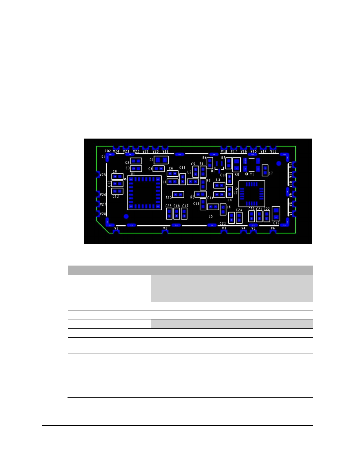
ARM Test Board for Certification
The following image shows the Aclara Radio module mounted on a test board
used for certification qualification.
The ARM Circuitry of the Test Board
There is a microcontroller that interfaces with the ARM using a Serial Peripheral
Interface (SPI). The SPI interface is where all data communications occur
between the Host microcontroller and the RF transceiver of the ARM. Both
commands and data are passed over the SPI interface. Digital signal levels for the
SPI interface are 3.6 V. The SPI interface uses buffered CMOS inputs and
outputs. There is a 64-byte TX/RX FIFO buffer internal to the Si4467. The SPI
interface only allows data transfer to the transceiver and has no effect on the
modulation or data rate of the RF transmitted signal.
A non-contact communication coil is used to control the test board and put the
radio into any desired operating mode. Aclara provides a communication puck
that when placed next to the communication coil, forms a loosely coupled
transformer. On-Off-Keying is then used at a baud rate of 1200 to pass bidirectional data between a controlling device (PC or handheld device) driving the
puck (via USB port) and the test board. This is only one method of
communicating with the ARM’s host microcontroller. Other methods such as
direct connect serial ports or opto-isolated serial interfaces can also be used to
control the host microcontroller in an end point device. Communications with the
host microcontroller is only required during production testing and device
installation. The interface for external host microcontroller communications will
not affect the signaling of the SPI interface for the ARM.
The power supply provides a regulated 3.6 VDC output to power the ARM module.
Nominal test board input voltage is 3.6 V, but it can be varied between 3.0 V and
4.2 V. The on-board power supply is a buck-boost topology and will keep
A c l a r a R a d i o M o d u l e I m p l e m e n t a t i o n R e q u i r e m e n t s 5
Page 7

DRAFT 8-1-2019 Technical Brief
Labeling
Étiquetage
The ARM will have a label containing the
Le module ARM portera une étiquette
Any Aclara product which uses the module
Tout produit Aclara qui utilise le module
CONTAINS: FCC ID: LLB2017025
CONTIENT
: ID FCC
: LLB2017025
IC: 4546A
-
2017025
IC : 4546A
-
2017025
The external label material will be the
Le matériau de l’étiquette extérieure sera
A sample label that contains the above
Un exemple d’étiquette contenant les
the ARM voltage at a regulated 3.6 VDC. The test board was designed to operate
over a single cell lithium battery voltage range in order to perform testing in RF
chambers without the requirement of an AC to DC power supply and the
associated conducted noise that can accompany them.
The JTAG port is for programming the host microcontroller. This is done once
during the production phase of the device. Any future revisions of device firmware
will be programmed over the JTAG port. The reset switch resets the
microcontroller if there is a need to do so.
The RF Output of the ARM connects to a 50-ohm controlled impedance strip-line
trace that connects to the SMA type RF connector. The RF connector is used to
make conducted RF measurements during certification testing.
This information should be enough to assure a proper installation of the ARM into
any new Aclara end point device that requires 450 MHz to 470 MHz licensed
narrow band RF transmission.
Labeling
FCC ID number and the ISED ID number
positioned on the top of the module shield. A
label with the HVIN number will also be on
the shield.
as the TX/RX portion of the circuit will have
a label on the outside of the product which
states that the product:
equivalent of 3M #7871, 2 mil, UV stable
gloss polyester, with high strength solvent
acrylic adhesive.
information is shown below.
contenant le numéro d’identification de la FCC
et le numéro d’identification de l’ISED dans le
haut du boîtier du module. Une étiquette
portant le numéro HVIN figurera également
sur le boîtier.
comme portion TX/RX du circuit portera en
surface une étiquette déclarant que le produit :
équivalent à 3M no 7871, 2 mil, polyester
lustré résistant aux UV avec adhésif acrylique
puissant à base de solvant.
informations qui précèdent est inclus cidessous.
A c l a r a R a d i o M o d u l e I m p l e m e n t a t i o n R e q u i r e m e n t s 6
Page 8

DRAFT 8-1-2019 Technical Brief
PRODUCT NAME
PRINT IN OPEN SANS BOLD 14 PT
NOM DU PRODUIT
IMPRIMÉ EN OPEN SANS GRAS 14 PT
PRODUCT SERIAL NUMBER (MAC ID)
SEE NOTE 5.
NUMÉRO DE SÉRIE DU PRODUIT (ID MAC)
VOIR LA NOTE 5.
DATA MATRIX 2D BARCODE
MATRICE DE DONNÉES SUR CODE À
VOIR LA NOTE 4.
CATALOG NUMBER
NUMÉRO DU CATALOGUE
CATALOG NU
MBER REVISION
NUMÉRO DE RÉVISION DU CATALOGUE
DEVICE PARAMETERS
PARAMÈTRES DE L’APPAREIL
DATE OF MANUFACTURE
DATE DE FABRICATION
IC NUMBER
NUMÉRO IC
FCC ID
ID FCC
PRINT IN OPEN SANS BOLD 10 PT
SEE NOTE 4.
IMPRIMÉ EN OPEN SANS GRAS 10 PT
BARRES 2D
Host Product Power Output
Any Aclara host product using the Aclara 101-2017-025 radio module will have the following
parameters:
Aclara Radio Module Rated Output Power
Standard Range 24.31 dBm 29.31 dBm EIRP
Extended Range 29.16 dBm 34.16 dBm EIRP
Conducted Power
Radiated Power with Max.Gain Antenna*
Maximum Range 30.31 dBm 35.31 dBm EIRP
Standard Range 237 mW 853 mW EIRP
Extended Range 824 mW 2606 mW EIRP
Maximum Range 1073 mW 3396 mW EIRP
*Maximum Antenna Gain = 5 dBi
A c l a r a R a d i o M o d u l e I m p l e m e n t a t i o n R e q u i r e m e n t s 7
Page 9

DRAFT 8-1-2019 Technical Brief
RF Exposure
Exposition aux RF
Host products using the ARM could perform
Les produits hôtes qui utilisent le module
Using the power levels given above with the
En utilisant les puissances données ci
-
dessus
Rang
e EIRP
Duty Cycle
Standard
853 mW EIRP
100%
Extended
2606 mW EIRP
32%
Maximum
3396 mW EIRP
25%
Portée
PIRE
Cycle de service
Standard
853 mW
PIRE
100 % Étendue
2606 mW
PIRE
32 %
Maximum
3396 mW
PIRE
25 %
RF Exposure
many different functions requiring different
operational parameters. The host product
will meet the FCC and ISED RF exposure
limitations for uncontrolled areas at a
distance >20 cm. This can be obtained with
the adjustment of power output, transmission
duty cycle, or both. For products that are to
be installed within a controlled area, the
exposure limits may be relaxed to the levels
required for controlled areas with the
addition of any warnings that might be
required for this situation.
max gain antenna, the following conditions
will meet the RF exposure limitation for
uncontrolled areas at a distance of 20 cm.
ARM pourraient effectuer différentes
fonctions qui requièrent des paramètres
d’exploitation variés. Le produit hôte
respectera les limites d’exposition aux RF de
la FCC et de l’ISED pour les zones non
contrôlées à une distance >20 cm. Cela peut
être obtenu en ajustant la puissance de sortie,
le cycle d’utilisation de la transmission, ou les
deux. Pour les produits pour installation dans
une zone contrôlée, les limites d’exposition
peuvent être allégées aux niveaux requis pour
les zones contrôlées avec l’ajout des
avertissements requis par la situation.
pour le gain d’antenne maximal, les conditions
suivantes respectent les limites d’exposition
aux RF pour les zones non contrôlées à une
distance de 20 cm.
A c l a r a R a d i o M o d u l e I m p l e m e n t a t i o n R e q u i r e m e n t s 8
 Loading...