

Page 1

1
Speedster22i sBus Interface
User Guide
UG047, October 24, 2013
UG047, October 24, 2013
Page 2

Copyright Info
Copyright © 2013 Achronix Semiconductor Corporation. All rights reserved. Achronix is a
trademark and Speedster is a registered trademark of Achronix Semiconductor Corporation.
All other trademarks are the property of their prospective owners. All specifications subject
to change without notice.
NOTICE of DISCLAIMER: The information given in this document is believed to be accurate
and reliable. However, Achronix Semiconductor Corporation does not give any
representations or warranties as to the completeness or accuracy of such information and
shall have no liability for the use of the information contained herein. Achronix
Semiconductor Corporation reserves the right to make changes to this document and the
information contained herein at any time and without notice. All Achronix trademarks,
registered trademarks, and disclaimers are listed at http://www.achronix.com and use of this
document and the Information contained therein is subject to such terms.
2 UG047, October 24, 2013
Page 3

3
Table of Contents
Copyright Info ......................................................................................................................... 2
List of Figures ........................................................................................................................ 5
List of Tables .......................................................................................................................... 6
Preface ............................................................................................................... 7
About this Guide .................................................................................................................... 7
Target Readership (or Audience) ........................................................................................... 7
Reference Documents ........................................................................................................... 7
Conventions used in this Guide ............................................................................................. 8
Terminologies used in this Guide ........................................................................................... 8
Chapter 1 – sBus Overview .............................................................................. 9
Introduction ............................................................................................................................ 9
Operation ............................................................................................................................. 10
Features ............................................................................................................................... 10
Bus .............................................................................................................................................. 10
Accessible IPs .............................................................................................................................. 10
Chapter 2 – sBus Functional Description ...................................................... 11
Port List ................................................................................................................................ 11
Read Operation .................................................................................................................... 11
32-bit Data-width Mode ................................................................................................................ 11
8-bit Data-width Mode .................................................................................................................. 12
Write Operation .................................................................................................................... 13
32-bit Data-width Mode ................................................................................................................ 13
8-bit Data-width Mode .................................................................................................................. 13
Chapter 3 – sBus Interfaces ........................................................................... 15
Master Interface ................................................................................................................... 15
Slave Interface ..................................................................................................................... 16
Chapter 4 – sBus Master Implementation ..................................................... 17
Single Master for Single Slave Implementation .................................................................... 17
Master Specifications for PLL sBus Controller .............................................................................. 17
Master Actions for PLL sBus Controller ........................................................................................ 17
UG047, October 24, 2013
Page 4

Read Operation ............................................................................................................................ 17
Write Operation ............................................................................................................................ 17
Single Master for Multiple Slaves Implementation ............................................................... 18
Master Specifications for Ethernet MAC and SerDes sBus Controller .......................................... 18
Master Actions for Ethernet MAC and SerDes sBus Controller .................................................... 18
Read Operation ............................................................................................................................ 18
Write Operation ............................................................................................................................ 18
Design Considerations ................................................................................................................. 18
Multiple Masters for a Single/Multiple Slave(s) Implementation ........................................... 19
Design Considerations ................................................................................................................. 19
Chapter 5 – sBus Design Examples ............................................................... 20
sBus Master Design ............................................................................................................. 20
Design Example ........................................................................................................................... 20
Master State Machine ................................................................................................ .................. 21
sBus Master Operation ........................................................................................................ 22
Clocking Considerations ...................................................................................................... 22
Appendix A – sBus Master Verilog Code....................................................... 23
Appendix B – Revision History ...................................................................... 27
4 UG047, October 24, 2013
Page 5

5
List of Figures
Figure 1: The HD1000 FPGA with sBus interfaces ................................................................................... 9
Figure 2: The sBus interface signals ......................................................................................................... 10
Figure 3: 32-bit Data Width sBus Read Operation ................................................................................... 12
Figure 4: 8-bit Data Width sBus Read Operation ..................................................................................... 12
Figure 5: 32-bit Data Width sBus Write Operation .................................................................................. 13
Figure 6: 8-bit Data Width sBus Write Operation .................................................................................... 14
Figure 7: Single Master for a single sBus Slave ....................................................................................... 15
Figure 8: Single Master for two sBus Slaves ............................................................................................ 16
Figure 9: sBus Slave Interface .................................................................................................................. 16
Figure 10: sBus Master Block Diagram.................................................................................................... 20
Figure 11: sBus Master State Machine ..................................................................................................... 21
UG047, October 24, 2013
Page 6

List of Tables
Table 1: HD1000 sBus Port Definition ..................................................................................................... 11
Table 2: HD1000 sBus Master Signal Definitions ................................................................................... 20
6 UG047, October 24, 2013
Page 7

7
Preface
About this Guide
The Achronix sBus is a serial bus implemented on the AC22IHD1000-F53C3 FPGA device to
allow users to access configuration registers for several of the Hard IPs available on the
device, through the FPGA fabric. This guide provides details on the implementation and uses
of the sBus. You will learn about the IP control registers that can be configured, status
registers, and how to access them for reads and writes, using the sBus, as appropriate.
Examples are provided to help you with the implementation of your own system designs.
This guide consists of the following chapters:
Chapter 1 – sBus Overview provides an overview of the sBus implemented on the
AC22IHD1000-F53C3 FPGA device.
Chapter 2 – sBus Functional Description covers more details of the sBus functionality.
Chapter 3 – sBus Interfaces describes the master and slave interfaces for the sBus.
Chapter 4 – sBus Master Implementation provides information about designing with the
sBus functional block.
Chapter 5 – sBus Design Examples provides detailed design examples for a single and
multiple IP access.
Appendix A – sBus Master Verilog Code provides a code example for a sample sBus
master design.
Appendix B – Revision History highlights the revisions to this document.
Target Readership (or Audience)
This guide is intended for embedded systems and sub-systems designers working with the
Achronix HD1000, 22-nm FPGA. You should have knowledge of FPGAs, Controllers,
Development environments and other relevant technologies.
This guide does not include board design and layout information. If you want assistance with
board design and layout, please contact Achronix.
Reference Documents
Speedster22i FPGA Family Datasheet (DS004)
Speedster22i Development Kit User Guide (UG034)
ACE User Guide (UG001)
Achronix Software & License User Guide (UG002)
Bitporter User Guide (UG004)
UG047, October 24, 2013
Page 8
Conventions used in this Guide
Item
Format
Examples
Command-line entries
Courier bold font face
$ Open top_level_name.log
File Names
Courier font face
filename.ext
GUI buttons, menus and
radio buttons
Helvetica bold font face
Click OK to continue.
File → Open
Variables
Italic emphasis
design_dir/output.log
Window and dialog box
headings and sub-headings
Heading in quotation
marks
Under “Output Files,” select ...
Window and dialog box
names
Initial caps
From the Add Files dialog box, ...
Terminology
Synonyms
Examples
Speedster22i
HD1000
Refers to the Achronix FPGA
family
sBus
Serial bus, SBUS
Refers to the serial bus on the
HD1000
This document uses the conventions shown in the following table.
Terminologies used in this Guide
This document uses the terminologies and synonyms shown in the following table.
8 UG047, October 24, 2013
Page 9
9
Chapter 1 – sBus Overview
Fabric
DDR
Interlaken
16-bit
Ethernet
MAC
32-bit
SerDes
PCIe
sBus
Port
Control
Logic
HD1000
Hard IP
Area
PLL
In this chapter, you will learn the following about the sBus serial bus:
Introduction
Operation
Features
Introduction
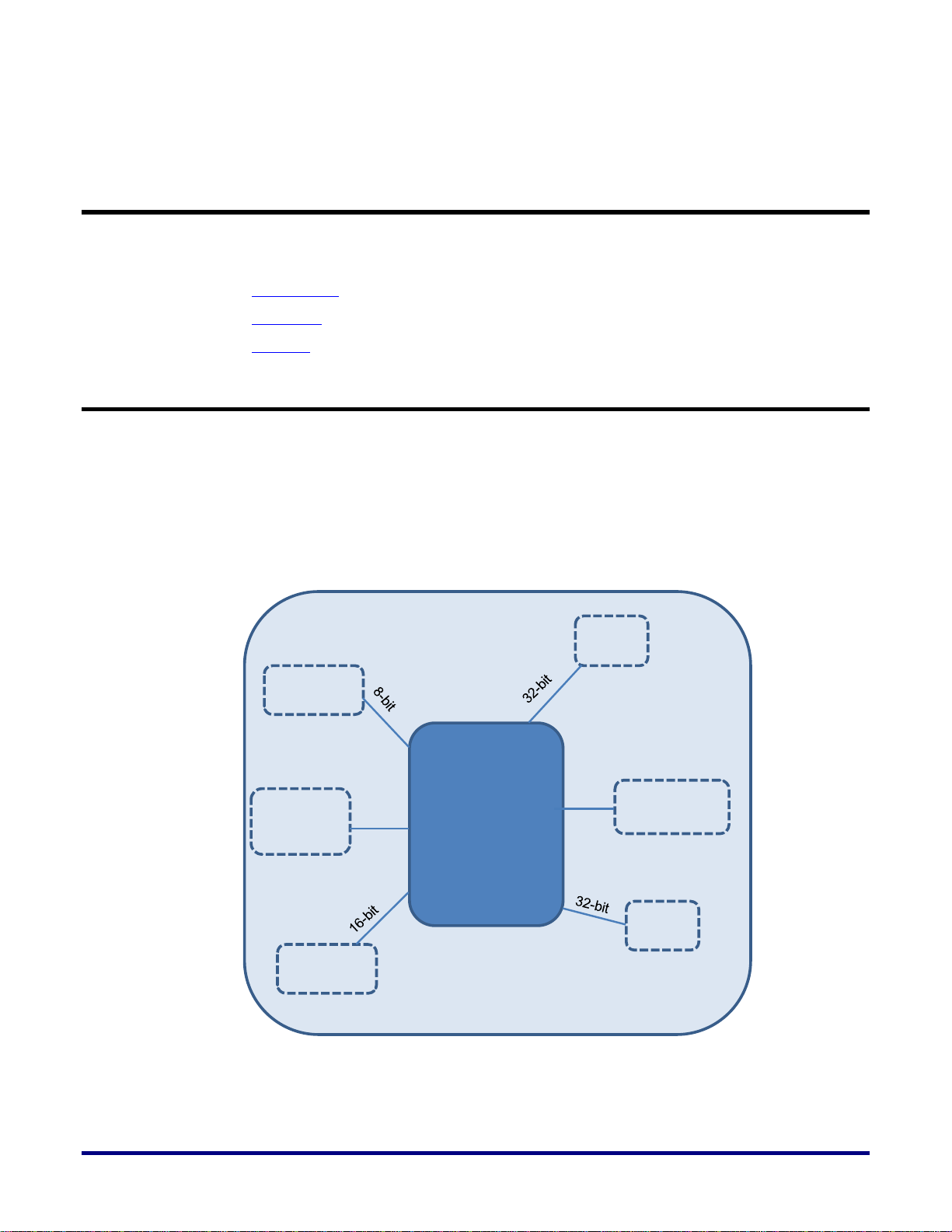
The sBus is a serial bus on the Achronix AC22IHD1000-F53C3 (“HD1000”) FPGA to enable
designers to communicate with registers on the Ethernet, SerDes, PCIe, Interlaken, and DDR
hard IPs. You can write to the IP registers to configure properties and read from the registers
to verify current configuration. The sBus provides communications between the FPGA fabric
and the interfaces of the hard IPs to the FPGA fabric. The control logic for the sBus is
implemented in the FPGA fabric.
Figure 1 shows the HD1000 FPGA with the sBus highlighted.
UG047, October 24, 2013
Note: PLL registers are 8-bit but the interface is 32-bit. Upper 24-bits are ignored.
Figure 1: The HD1000 FPGA with sBus interfaces
Page 10

Operation
Hard IP
sBus
Port
Fabric
sBus Port
Control
Logic
sbus_clk
reset_sbus_clk
i_sbus_req
i_sbus_data[1:0]
o_sbus_ack
o_sbus_data[1:0]
Registers
The sBus takes serial data from the FPGA fabric sBus control logic (“Fabric”) and transmits it
over a 2-bit data bus to the hard IP sBus interface for writes. For reads, the sBus takes 2-bit
serial data from the hard IP to the Fabric. During a write operation, the Fabric converts the
parallel data, 8-, 16-, or 32-bit wide and serializes it. The Fabric presents the address of the
register to be written to and the data to the IP interface over the 2-bit serial bus. For read
operations, the Fabric presents the address for the read operation to the IP interface and the
the hard IP responds by placing the 2-bit serialized data on the sBus.
The sBus can operate such that a single IP is accessed or in a master-slave mode such that
multiple IPs can be accessed.
Figure 2 shows the signals used for communications between the Fabric and the hard IP,
which includes the logic to receive and convert the write address and data to the correct
format for updating the registers. For reads, the register data is converted from parallel to
serial for presentation to the sBus by the hard IP block.
Figure 2: The sBus interface signals
Features
Bus
2-bit serial data width
8-, 16-, or 32-bit parallel data
Single clock
Accessible IPs
Ethernet
SerDes
10 UG047, October 24, 2013
PCIe
Interlaken
DDR
PLL
Page 11

11
Chapter 2 – sBus Functional Description
Port
Direction
Description
reset_sbus_clk
Input
Asynchronous reset
sbus_clk
Input
Reference clock for the serial
and parallel interfaces –
p1_ctl_clk
i_sbus_req
Input
Request signal for starting a
read or write transaction on
sBus.
i_sbus_data[1:0]
Input
Input serial data of sBus
interface.
o_sbus_data[1:0]
Output
Output serial data of sBus
interface.
o_sbus_ack
Output
Acknowledgement signal for
read and write operation
complete on sBus interface.
In this chapter, you will learn the following about the sBus serial bus:
Port List
Read Operation
Write Operation
Port List
The sBus interface or port uses eight signals for operation. Table 1 lists these signals and their
functions. These signals can be driven directly by a state machine in the FPGA fabric. You can
find more information about designs based on these topologies in Chapter_3 detailing the
Master and Slave interface sections.
Table 1: HD1000 sBus Port Definition
Read Operation
UG047, October 24, 2013
32-bit Data-width Mode
For a 32-bit data-width mode read operation, you must do the following.
1. Assert the i_sbus_req signal for 9 cycles.
2. De-assert i_sbus_data[0] during the first cycle.
3. Send the LSB of the 17-bit long read address on i_sbus_data[1] during the first cycle.
4. Send the remaining 16 bits of the read address on i_sbus_data[1:0] in the following order
[A2:A1]…[A16:A15] over the next 8 cycles.
5. De-assert i_sbus_req signal.
The sBus slave will decode the read operation and respond as follows.
Page 12

6. Assert the o_sbus_ack signal, when data is ready.
7. Transmit the serial data on the o_sbus_data[1:0] signals using the ordering [D1:D0]…
[D31:D30] in 16 cycles.
8. De-assert the o_sbus_ack signal after 16 cycles, when the transmission is complete.
Figure 3 shows the timing diagram for a 32-bit data width, sBus read operation.
Figure 3: 32-bit Data Width sBus Read Operation
8-bit Data-width Mode
For an 8-bit data-width mode read operation, you must do the following.
1. Assert the i_sbus_req signal for 9 cycles.
2. De-assert i_sbus_data[0] during the first cycle.
3. Send the LSB of the 17-bit long read address on i_sbus_data[1] during the first cycle.
4. Send the remaining 16 bits of the read address on i_sbus_data[1:0] in the following order
[A2:A1]…[A16:A15] over the next 8 cycles.
5. De-assert i_sbus_req signal.
The sBus slave will decode the read operation and respond as follows.
6. Assert the o_sbus_ack signal, when data is ready.
7. Transmit the serial data on the o_sbus_data[1:0] signals using the ordering [D1:D0]…
[D7:D6] in 4 cycles.
8. De-assert the o_sbus_ack signal after 4 cycles, when the transmission is complete.
Figure 4 shows the timing diagram for an 8-bit data width, sBus read operation.
Figure 4: 8-bit Data Width sBus Read Operation
12 UG047, October 24, 2013
Page 13

13
Write Operation
32-bit Data-width Mode
For a 32-bit data-width mode write operation, you must do the following.
1. Assert the i_sbus_req signal for 25 cycles.
2. Assert i_sbus_data[0] during the first cycle.
3. Send the LSB of the 17-bit long write address on i_sbus_data[1] during the first cycle.
4. Send the remaining 16 bits of the read address on i_sbus_data[1:0] in the following order
[A2:A1]…[A16:A15] over the next 8 cycles.
5. Send the 32-bit data on i_sbus_data[1:0] in the following order [D1:D0]…[D31:D30].
6. De-assert i_sbus_req signal.
The sBus slave will decode and complete the write operation and respond as follows.
7. Assert the o_sbus_ack signal to indicate the end of the write operation.
Figure 5 shows the timing diagram for a 32-bit data width, sBus write operation.
Figure 5: 32-bit Data Width sBus Write Operation
8-bit Data-width Mode
For an 8-bit data-width mode write operation, you must do the following.
1. Assert the i_sbus_req signal for 13 cycles.
2. Assert i_sbus_data[0] during the first cycle.
3. Send the LSB of the 17-bit long write address on i_sbus_data[1] during the first cycle.
4. Send the remaining 16 bits of the read address on i_sbus_data[1:0] in the following order
[A2:A1]…[A16:A15] over the next 8 cycles.
5. Send the 8-bit data on i_sbus_data[1:0] in the following order [D1:D0]…[D7:D6].
6. De-assert i_sbus_req signal.
The sBus slave will decode and complete the write operation and respond as follows.
7. Assert the o_sbus_ack signal to indicate the end of the write operation.
Figure 6 shows the timing diagram for an 8-bit data width, sBus write operation.
UG047, October 24, 2013
Page 14

Figure 6: 8-bit Data Width sBus Write Operation
14 UG047, October 24, 2013
Page 15

15
Chapter 3 – sBus Interfaces
Fabric
sBusPort
Control
Logic
sbus_clk
reset_sbus_clk
i_sbus_req
i_sbus_data[1:0]
o_sbus_ack
o_sbus_data[1:0]
In this chapter, you will learn the following about the sBus serial bus:
Master Interface
Slave Interface
Master Interface
You have the flexibility to design the sBus master depending on your needs. You could, for
example, do the following.
Design one master to address only one slave
Design one master to address multiple slaves
Design one master to accept data from multiple sources and direct it to one slave
Or design such combinations of each or any of the above
Figure 7 shows a single master generating and accepting the required signals for writes and
reads to the slave interface.
UG047, October 24, 2013
Figure 7: Single Master for a single sBus Slave
Figure 8 shows a single master generating and accepting the required signals for writes and
reads to two slave interfaces.
Page 16

Fabric
sBus Port
Control
Logic
sbus_clk
reset_sbus_clk
i_sbus_req
i_sbus_data [1:0]
o_sbus_ack
o_sbus_data [1:0]
Slave 1
Slave 2
Note: Achronix provides design examples for some of these implementations. Contact Achronix for
Hard IP
sBus
Port
sbus_clk
reset_sbus_clk
i_sbus_req
i_sbus_data[1:0]
o_sbus_ack
o_sbus_data[1:0]
Registers
more information and help with your specific needs.
Slave Interface
The sBus slave interface typically has an 8-pin port as shown in Figure 9. For IPs that use
multiple lanes, for example, PCIe, the slave interface has the appropriate number of such
signal sets, and you must design the master accordingly. Refer to the Speedster22i PCIe User
Guide (UG030) for more details on the PCIe implementation.
Figure 8: Single Master for two sBus Slaves
Figure 9: sBus Slave Interface
16 UG047, October 24, 2013
Page 17

17
Chapter 4 – sBus Master Implementation
In this chapter, you will learn the following about the sBus serial bus:
Single Master for Single Slave Implementation
Single Master for Multiple Slaves Implementation
Multiple Masters for a Single/Multiple Slave(s) Implementation
The sBus design consists primarily of defining and implementing the master control block in
the HD1000 FPGA fabric. As discussed in the Master Interface section, you have a lot of
flexibility to implement the master, based on your needs, and the slave interface of the IP for
which you need the master. Discussing all the options is beyond the scope of this guide. The
following sections highlight a few typical examples. For your specific needs, contact
Achronix.
Single Master for Single Slave Implementation
You can use a single sBus master to communicate with a single sBus slave on a hardened IP
such as a PLL on the HD1000, which has several independent PLLs on board. You can get
more information about the slave interface for the specific IP from the relevant User Guide. In
this case, the master must have the following specifications.
Master Specifications for PLL sBus Controller
32-bit data width (the slave will only use the lower 8-bits so there is room for design
simplification)
8 pins to drive the PLL sBus slave interface
Pins to receive the register programming information from the user on the fabric side
Pins to provide register/status information to the user on the fabric side
Master Actions for PLL sBus Controller
Read Operation
1. Receive information from the user for the read request on the fabric side.
2. Drive the read actions on the sBus as explained for 32-bit reads in 32-bit Data-width
Mode.
3. Monitor the o_sbus_ack signal to accept the serial data from the PLL sBus slave.
Note: You can simplify your design to accept only the lower 8-bits of data.
4. Latch the serial data and provide it to the user on the fabric side.
Write Operation
1. Receive information from the user for the write request on the fabric side.
2. Drive the write actions on the sBus as explained for 32-bit writes in 32-bit Data-width
Mode.
UG047, October 24, 2013
Page 18

3. Monitor the o_sbus_ack signal from the PLL sBus slave signaling the end of the write
request.
Note: You can simplify your design to send a fixed data pattern for the upper 24-bits.
4. Inform the user on the fabric side of the completion of the write request.
Single Master for Multiple Slaves Implementation
You can use a single sBus master to communicate with multiple sBus slaves on a hardened IP
such as the Ethernet MAC and SerDes on the HD1000. You can get more information about
the slave interfaces for the specific IP from the relevant User Guide. In the case of the
Ethernet MAC and the associated SerDes, the master must have the following specifications.
Master Specifications for Ethernet MAC and SerDes sBus
Controller
32-bit data width for the MAC
8-bit data width for the 12 SerDes
104 (8 x 13) pins to drive each of the 13 Ethernet sBus slave interfaces
Pins to receive the register programming information from the user on the fabric side
Pins to provide register/status information to the user on the fabric side
Master Actions for Ethernet MAC and SerDes sBus Controller
Read Operation
1. Receive information from the user for the read request on the fabric side.
2. Drive the read actions on the sBus.
a. 32-bit Data-width Mode for the MAC registers
b. 8-bit Data-width Mode for the SerDes registers
3. Monitor the o_sbus_ack signal from the appropriate IP block to accept the serial data from
the sBus slave.
4. Latch the serial data and provide it to the user on the fabric side.
Write Operation
1. Receive information from the user for the write request on the fabric side.
2. Drive the write actions on the sBus.
a. 32-bit Data-width Mode for the MAC registers
b. 8-bit Data-width Mode for the SerDes registers
3. Monitor the o_sbus_ack signal from the appropriate IP sBus slave signaling the end of the
write request.
4. Inform the user on the fabric side of the completion of the write request.
Design Considerations
Depending on your application and the register(s) accessed, you may have to take additional
actions to ensure predictable behavior of the IP core and your application. For example, you
may have to ensure that all the SerDes registers are updated before transmissions based on
the new configuration are started. If multiple registers in different IP blocks require updates
18 UG047, October 24, 2013
Page 19

19
before a specific action, you must also consider latencies in the design to ensure that the
delay from the slowest sBus link is acceptable for the application.
Multiple Masters for a Single/Multiple Slave(s) Implementation
You can treat the multiple masters for a single/multiple slave implementation as an extension
of the Single Master for Single Slave Implementation and/or a Single Master for Multiple
Slaves Implementation because the multiple masters can be implemented as a single master
controller with multiple user sources.
Design Considerations
You must include additional inputs to accept, and outputs to provide the user information
from and to the fabric side respectively. You must include logic in the controller to select the
appropriate inputs for writes and present it to the sBus interface for which the write request
is intended. When you have multiple slaves in the design, the controller should have the
logic to select the correct slave interface for the sBus channel from the supported set of such
interfaces. Similar actions must be taken by the master controller to read the requested slave
register and provide the information to the requester.
You must include some arbitration logic in the controller to ensure that each requesting
source is serviced within the acceptable constraints of the required application. Discussions
of such constraints are beyond the scope of this guide. Please contact Achronix for support as
needed.
UG047, October 24, 2013
Page 20

Chapter 5 – sBus Design Examples
Signal
Direction
Description
i_rst_n
Input
Asynchronous reset
i_clk
Input
Reference clock for the serial
and parallel interfaces –
sbus_clk
o_sbus_req
Output
Request signal for starting a
read or write transaction on
sBus
i_sbus_data[1:0]
Input
Input serial data of sBus
sbus_clk
reset_sbus_clk
o_sbus_req
o_sbus_data[1:0] (to slave)
i_sbus_ack
i_sbus_data[1:0] (from slave)
Master
Latched Parallel Data
i_reg_address [16:0]
i_sw_rst
i_reg_rw_req
i_reg_wr_data [Pbus_Data_Width - 1:0]
i_reg_write
o_reg_rd_data [Pbus_Data_Width - 1:0]
i_rst_n
i_clk
o_reg_rdwr_valid
Serializer/
Deserializer
In this chapter, you will learn the following about the sBus serial bus:
sBus Master Design
sBus Master Operation
Clocking Considerations
sBus Master Design
You will design and implement the sBus master in the HD1000 fabric. Figure 10 shows a
typical block diagram of a master implementation showing the interface to the parallel data
side (requester) and the sBus port (slave or hard IP) side.
20 UG047, October 24, 2013
Figure 10: sBus Master Block Diagram
Design Example
You will find the Verilog code for a sample master module implementation in Appendix A.
Table 2 describes the signals and their functions for this implementation.
Table 2: HD1000 sBus Master Signal Definitions
Page 21

21
Signal
Direction
Description
interface (from slave)
o_sbus_data[1:0]
Output
Output serial data of sBus
interface (to slave)
i_sbus_ack
Input
Acknowledgement signal for
read and write operation
complete on sBus interface
o_reg_rdwr_valid
Output
Read write operation
complete indication for
parallel interface
o_reg_rd_data[Pbus_Data_Width-1:0]
Output
Parallel Read data
i_reg_wr_data[Pbus_Data_Width-1:0]
Input
Parallel Write data
i_sw_rst
Input
Software reset when ack not
received
i_reg_address[16:0]
Input
Reg rd/wr address
i_reg_write
Input
Write operation on parallel
interface
i_reg_rw_req
Input
Read operation on parallel
interface
ST_SBUS_IDLE ST_SBUS_ADDR
ST_SBUS_WR_DATAST_SBUS_RD_DATA
ST_SBUS_WR
start_sbus_transfer
&rdwr_data_cnt
is_write&& (addr_cnt == 3’d7)
i_sbus_ack
~i_sbus_ack
addr_cnt!= 3’d7~start_sbus_transfer
~&rdwr_data_cnt
~&rdwr_data_cnt
Master State Machine
Figure 11 shows the state machine for the sBus master implementation for the above
example.
UG047, October 24, 2013
Figure 11: sBus Master State Machine
Page 22

sBus Master Operation
The sBus master will move from the ST_SBUS_IDLE to the ST_SBUS_ADDR state when you
assert the i_sbus_req signal. Depending on whether the request is for a write or a read, as
determined by the state of the i_sbus_data[0] signal, the state machine will transition to
the ST_BUS_WR_DATA or ST_BUS_RD_DATA and after the completion of the cycle
transition back to the ST_BUS_IDLE state.
Clocking Considerations
Most sBus channels must be operated at under 50 MHz clock speeds. The following code
fragment shows a typical example, where the clock has been set to 16 MHz for the Ethernet
IP interface.
#### -------- CLOCK INFORMATION -------- ####
create_clock -period 10.0 pll_ref_clk
create_clock -period 62.5
{iSBUS_CLK_PLL.NE_APLL_0_gui_ne_pll_APLL.iACX_PLL/ogg_gm_clk[0]} -name
sbus_clk
######------------ DONE -----------#########
22 UG047, October 24, 2013
Page 23

23
Appendix A – sBus Master Verilog Code
//
// Module Name : sbus_master_if
//
// Description : SBUS master module to transfer parallel register data in
// serial mode to reduce the number of status ports.
//
module sbus_master_if #(parameter PBUS_DATA_WIDTH = 8) (
// SBUS Interface
input [1:0] i_sbus_d,
input i_sbus_ack,
output [1:0] o_sbus_d,
output o_sbus_req,
// Generic Register Interface
input i_reg_write,
input i_reg_rw_req,
input [16:0] i_reg_address,
input [PBUS_DATA_WIDTH-1:0] i_reg_wr_data,
output [PBUS_DATA_WIDTH-1:0] o_reg_rd_data,
output reg o_reg_rdwr_valid,
// Generic signals
// Reset the StateMachine if ack is not received
input i_sw_rst,
input i_clk,
input i_rst_n
);
//Function to calculate the size from the PBUS_WIDTH
// Start of Function
function integer c_log_b;
input integer depth;
integer i;
begin
c_log_b = 1;
for (i=0; 2**i < depth; i=i+1)
c_log_b = i+1;
end
endfunction
// End of Function
/////////////////////////////////////////////////
localparam CNTR_SIZE = c_log_b (PBUS_DATA_WIDTH/2);
reg [2:0] address_cnt;
reg [1:0] data_in_dly;
reg [(CNTR_SIZE-1):0] rdwr_data_cnt;
reg [4:0] sbus_cs;
reg [16:0] rw_address;
reg [PBUS_DATA_WIDTH-1:0] rd_data_shift_in,write_data;
reg [PBUS_DATA_WIDTH+17:0] addr_data_shift_in;
wire [17:0] addr_req;
reg is_write,req_dly,req_dly2,sbus_req_dly;
wire start_sbus_transfer,sbus_req;
//////////////////////////////////////////////////////////////////////
parameter ST_SBUS_IDLE = 5'b00001;
UG047, October 24, 2013
Page 24

parameter ST_SBUS_ADDR = 5'b00010;
parameter ST_SBUS_WR_DATA = 5'b00100;
parameter ST_SBUS_WR = 5'b01000;
parameter ST_SBUS_RD_DATA = 5'b10000;
/////////////////////////////////////////////////
always @(posedge i_clk or negedge i_rst_n)
begin
if (!i_rst_n)
begin
req_dly <= 1'b0;
req_dly2 <= 1'b0;
write_data <= {PBUS_DATA_WIDTH{1'b0}};
rw_address <= 'b0;
is_write <= 1'b0;
sbus_req_dly <= 1'b0;
end
else
begin
req_dly <= i_reg_rw_req;
req_dly2 <= req_dly;
sbus_req_dly <= sbus_req;
if (i_reg_rw_req && ~req_dly)
begin
is_write <= i_reg_write;
write_data <= i_reg_wr_data;
rw_address <= i_reg_address;
end
end
end
assign start_sbus_transfer = req_dly && ~req_dly2;
assign addr_req = {rw_address,is_write};
//////////////////////////////////////////////////////////////////////
// SBUS State Machine
//////////////////////////////////////////////////////////////////////
always @(posedge i_clk or negedge i_rst_n)
begin
if (!i_rst_n)
sbus_cs <= ST_SBUS_IDLE;
else if (i_sw_rst)
sbus_cs <= ST_SBUS_IDLE;
else
begin
case (sbus_cs)
ST_SBUS_IDLE : begin
if (start_sbus_transfer)
sbus_cs <= ST_SBUS_ADDR;
else
sbus_cs <= ST_SBUS_IDLE;
end
ST_SBUS_ADDR : begin
if (is_write && (address_cnt == 3'd7))
sbus_cs <= ST_SBUS_WR_DATA;
else if (address_cnt == 3'h7)
sbus_cs <= ST_SBUS_RD_DATA;
else
sbus_cs <= ST_SBUS_ADDR;
end
ST_SBUS_WR_DATA:begin
if (&rdwr_data_cnt)
sbus_cs <= ST_SBUS_WR;
else
24 UG047, October 24, 2013
Page 25

25
sbus_cs <= ST_SBUS_WR_DATA;
end
ST_SBUS_WR : begin
if (i_sbus_ack)
sbus_cs <= ST_SBUS_IDLE;
else
sbus_cs <= ST_SBUS_WR;
end
ST_SBUS_RD_DATA :begin
if (&rdwr_data_cnt)
sbus_cs <= ST_SBUS_IDLE;
else
sbus_cs <= ST_SBUS_RD_DATA;
end
default : begin
sbus_cs <= ST_SBUS_IDLE;
end
endcase
end
end
////////////////////////////////////////////////////////////////
// Address shift counter
////////////////////////////////////////////////////////////////
always @(posedge i_clk or negedge i_rst_n)
begin
if (!i_rst_n)
address_cnt <= 'h0;
else
begin
if (sbus_cs[1])
address_cnt <= address_cnt + 1'b1;
else
address_cnt <= 'h0;
end
end
////////////////////////////////////////////////////////////////
// Parallel to serial address conversion
////////////////////////////////////////////////////////////////
always @(posedge i_clk or negedge i_rst_n)
begin
if (!i_rst_n)
addr_data_shift_in <= 'h0;
else
if (start_sbus_transfer)
addr_data_shift_in <= {write_data,addr_req};
else if (sbus_cs[1] || sbus_cs[2])
addr_data_shift_in <=
{2'b00,addr_data_shift_in[PBUS_DATA_WIDTH + 17:2]};
end
assign o_sbus_d = addr_data_shift_in[1:0];
assign sbus_req = sbus_cs[1] || sbus_cs[2];
assign o_sbus_req = sbus_req || sbus_req_dly;
always @(posedge i_clk or negedge i_rst_n)
begin
if (!i_rst_n)
o_reg_rdwr_valid <= 1'b0;
else
UG047, October 24, 2013
Page 26

if ((sbus_cs[3] && i_sbus_ack) || (sbus_cs[4] &&
(&rdwr_data_cnt)))
o_reg_rdwr_valid <= 1'b1;
else
o_reg_rdwr_valid <= 1'b0;
end
////////////////////////////////////////////////////////////////
// RD/WR DATA shift counter
////////////////////////////////////////////////////////////////
always @(posedge i_clk or negedge i_rst_n)
begin
if (!i_rst_n)
rdwr_data_cnt <= 'b0;
else
begin
if (sbus_cs[2] || (sbus_cs[4] && i_sbus_ack))
rdwr_data_cnt <= rdwr_data_cnt + 1;
else
rdwr_data_cnt <= 'b0;
end
end
////////////////////////////////////////////////////////////////
// Write data Shift, Serial to parallel conversion
////////////////////////////////////////////////////////////////
always @(posedge i_clk or negedge i_rst_n)
begin
if (!i_rst_n)
rd_data_shift_in <= 'b0;
else
if (sbus_cs[4] && i_sbus_ack)
rd_data_shift_in <=
{i_sbus_d[1:0],rd_data_shift_in[PBUS_DATA_WIDTH-1:2]};
else
rd_data_shift_in <= 'b0;
end
assign o_reg_rd_data = rd_data_shift_in;
endmodule
26 UG047, October 24, 2013
Page 27

27
Appendix B – Revision History
Date
Version
Revisions
10/24/2013
1.0
Initial Achronix release.
The following table lists the revision history of this document.
UG047, October 24, 2013
 Loading...