

Page 1

Speedster22i DDR3 Controller
User Guid e
UG031 – Nov 18, 2014
UG031, Nov 18, 2014
1
Page 2

Copyright Info
Copyright © 2014 Achronix Semiconductor Corporation. All rights reserved. Achronix is a
trademark and Speedster is a registered trademark of Achronix Semiconductor Corporation.
All other trademarks are the property of their prospective owners. All specifications subject
to change without notice.
NOTICE of DISCLAIMER: The information given in this document is believed to be accurate
and reliable. However, Achronix Semiconductor Corporation does not give any
representations or warranties as to the completeness or accuracy of such information and
shall have no liability for the use of the information contained herein. Achronix
Semiconductor Corporation reserves the right to make changes to this document and the
information contained herein at any time and without notice. All Achronix trademarks,
registered trademarks, and disclaimers are listed at
document and the Information contained therein is subject to such terms.
http://www.achronix.com and use of this
2 UG031, Nov 18, 2014
Page 3

Table of Contents
Table of Figures ................................................................................................. 4
Features ............................................................................................................. 6
Introduction ....................................................................................................... 7
Interfaces ........................................................................................................... 9
Internal (core) Interface .......................................................................................................... 9
External (off-chip) Interface .................................................................................................. 11
Parameters .......................................................................................................................... 11
Address Mapping ............................................................................................ 14
Write Interface Details ..................................................................................... 15
Back-to-Back Write Protocol 2X Cloc k Mode ....................................................................... 19
Write Protocol with Wide Bus Interface Enabled .................................................................. 21
Read Interface Details ..................................................................................... 23
Back-to-Back Read Protocol 2X Clock Mode ....................................................................... 25
Read Protocol with Wide Bus Interface Enabled .................................................................. 27
Memory Interface Latency .............................................................................. 30
Customization using ACE ............................................................................... 31
Revision Histor y .............................................................................................. 32
UG031, Nov 18, 2014
3
Page 4

Tabl e of Fig ur es
Figure 1: Location of Speedster22i DDR Controllers and PHYs ............................................................... 5
Figure 2: Top-level Overview of Embedded DDR Control Logic ............................................................... 7
Figure 3: Address mapping of ‘ddr_int_addr’ Signal ............................................................................... 14
Figure 4: Write Interface 2X Clock Mode ................................................................................................. 15
Figure 5: Internal Interface Write Protocol Timing Diagram .................................................................. 16
Figure 6: Internal Interface Write Protocol Timing Diagram with default value ‘addrcmd_delay’ to 8 . 17
Figure 7: Write Protocol Timing Diagram (SDRAM Interface) ............................................................... 18
Figure 8: Write Protocol Timing Diagram (Write requests with valid writes highlighted)...................... 19
Figure 9: Write Protocol Timing Diagram (ddr_int_wrdata_req corresponding to respective writes
highlighted) ............................................................................................................................................... 20
Figure 10: Write Interface with Wide Bus Interface Enabled ................................................................... 22
Figure 11: Internal Interface Write Protocol Timing Diagram with Wide Bus Interface Enabled .......... 22
Figure 12: Read Interface 2X Clock Mode ............................................................................................... 24
Figure 13: Internal Interface Read Protocol Timing Diagram ................................................................. 24
Figure 14: External Interface Read Protocol Timing Diagram ................................................................ 25
Figure 15: Read Protocol Timing Diagram (with valid read request highlighted) .................................. 26
Figure 16: Read Protocol Timing Diagram (with ddr_int_rddata_valid highlighted) ............................. 26
Figure 17: Read Interface with Wide Bus Interface Enabled ................................................................... 28
Figure 18: Internal Interface Read Protocol Timing Diagram with Wide Bus Interface Enabled ........... 28
Figure 19: DDR3 Customization using ACE ............................................................................................ 31
4 UG031, Nov 18, 2014
Page 5
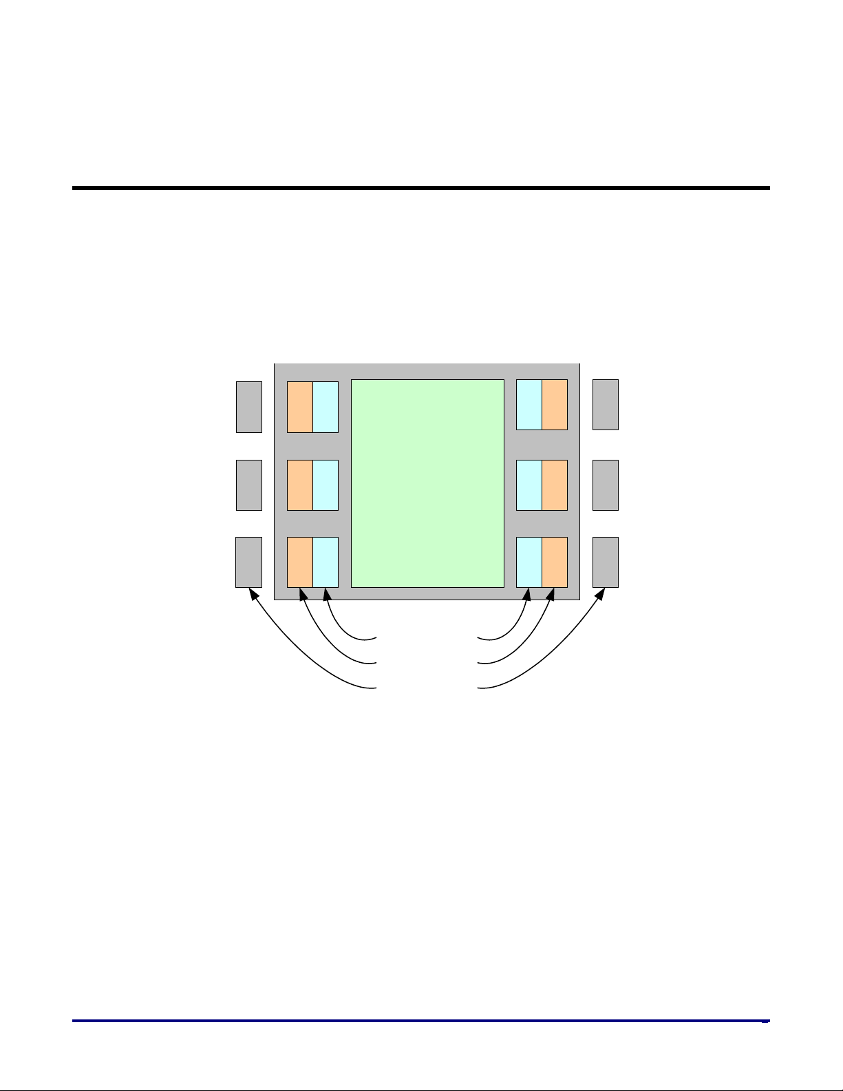
Overview
Speedster22i FPGA
DDR PHY
DDR Controller
DDR Memory
(off-chip)
Speedster22i Core
WN
WS
EN
ES
EC
WC
Achronix’s Speedster22i FPGAs contain up to six embedded DDR controllers which can be
used to interface with and control off-chip DDR2 or DDR3 memory devices, including
DIMMs. Each of the DDR controllers supports up to 72 bits of data and speeds of up to 1866
Mbps. The embedded DDR controllers and PHYs are implemented as Hard-IP blocks in the
frame of the Speedster22i FPGAs as illustrated in Figure 1 below.
UG031, Nov 18, 2014
Figure 1: Location of Speedster22i DDR Controllers and PHYs
Speedster22i DDR controllers support both “auto” and “custom” modes. Under the “auto”
mode functions such as (but not limited to) activating/precharging banks/rows, calibration
algorithms, and initialization sequences are handled by the embedded DDR Controller and
are transparent to the user. The mapping of byte-lanes to pins is also handled transparently
as the IOs are included in embedded DDR PHY Macro.
Under “custom” mode the user has the option to manually override functions such as
automated refresh and initialization engines/sequences.
5
Page 6

Features
The features supported by the embedded DDR controllers are highlighted below:
• 1866 Mbps data rate
• The controller and PHY can run at 1066 MHz to achieve 1866 Mbps rate at the
memory interface. A 2X Clock setting enables the core to run at half the speed 533MHz. There is an additional feature to enable a wide bus interface, which
effectively enables the core to run at one quarter the speed - 266MHz. The 2X
clock setting and wide bus interfaces can be enabled at any data rate, thereby
reducing the core frequency by half, or a quarter, respectively.
• 4 Chip Selects per controller
• The external memory connected to each controller can comprise of up to 4 ranks
(either two dual-rank DIMMs or one quad rank DIMM)
• Registered DIMM and Unbuffered DIMM support
• Each controller can independently support either rDIMMs or uDIMMs
• Address mirroring is supported.
• Multi-Burst Mode
• Each controller supports multi-burst mode, up to a burst length of 252 (DDR2) /
254 (DDR) / 248(DDR3). This allows the embedded controller to automatically
issue up to 252 cascaded read or write commands to automatically increment
addresses based on a single command from the Core Fabric
• Backwards Compatible
• The embedded DDR controllers can support DDR3 (up to 1866 Mbps), DDR2 (up
to 800 Mbps) and DDR protocols
• Bypassable
• If the user does not require all six DDR controllers, any (or all) can be bypassed
to leverage use of the designated I/Os for other purposes
• If the user does not require all 72-bits of the data bus, unused byte lanes can be
bypassed to leverage use of the designated I/Os for other purposes
• Minimal LUT use
• The DDR controllers are embedded (hardened), and therefore do not use any of
the LUTs in the core fabric
• LUTs are only required to interface the DDR Controllers
• Zero License fees
6 UG031, Nov 18, 2014
Page 7
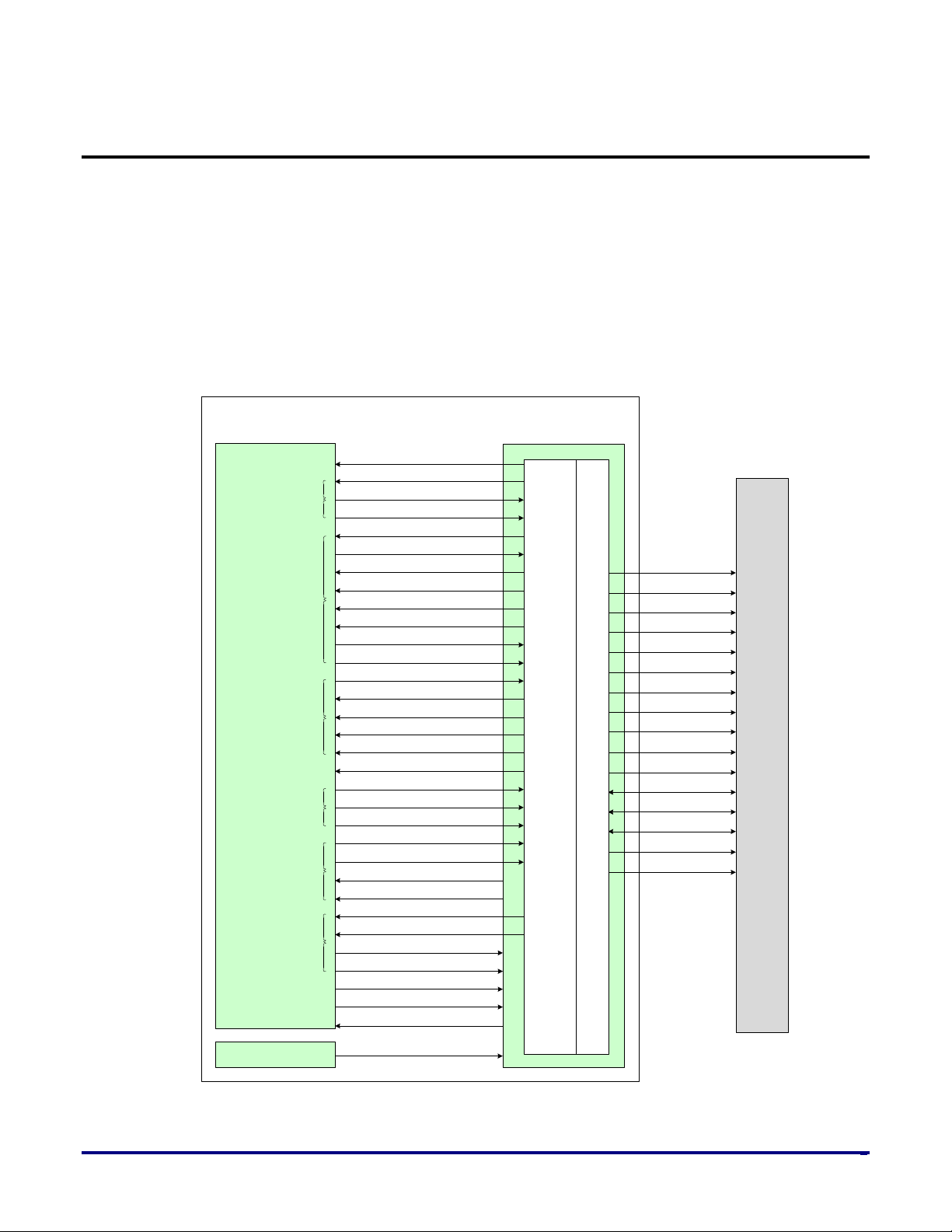
Introduction
Speedster22i
DDR Control Macro
ACX_PLL
DDR
Controller
clk
sd_dummy[8:0]
sd_dm[8:0]
sd_dqsn[8:0]
sd_dqsp[8:0]
sd_dq[71:0]
sd_cke[3:0]
sd_clk_out_p[3:0]
sd_clk_out_n[3:0]
sd_reset_n
sd_cas_n
sd_ras_n
sd_we_n
sd_a[15:0]
sd_ba[2:0]
sd_cs_n[3:0]
sd_odt[3:0]
Read/Write
Shared Interface
Write Interface
Read Interface
General Memory
Control Interface
Manual refresh
control Interface
Control
Interface
DDR Internal Interface
(User Logic)
ddr_int_clk_div2
ddr_int_zq_cal_ack
ddr_int_ref_ack
ddr_int_busy_align
ddr_int_busy
ddr_int_wrdata_valid
ddr_int_wrdata_req[8:0]
ddr_int_wrdata_req_early[8:0]
ddr_int_wrdata_req_align[8:0]
ddr_int_wrdata_req_early_align[8:0]
ddr_int_rddata[287:0]
ddr_int_rddata_valid [8:0]
ddr_int_rddata_valid_align[8:0]
ddr_int_rddata_valid_early[8:0]
ddr_int_rddata_valid_early_align[8:0]
ddr_int_init_ack
ddr_int_init_wlvl_done
ddr_int_cmd_auto_pch
ddr_int_cmd_self_refresh[1:0]
ddr_int_addr[33:0]
ddr_int_burst_size[7:0]
ddr_int_wr_request
ddr_int_wrdata[287:0]
ddr_int_wrdata_mask[17:0]
ddr_int_rd_request
reset_ddr_ctrlr_n
reset_ddr_phy_n
ddr_int_phy_ci_slave_dqsn_en
ddr_int_cmd_power_down[1:0]
ddr_int_cmd_ref_req
ddr_int_cmd_zq_cal_req[1:0]
ddr_int_phy_ci_slave_adj
DDR
PHY
External
DDR Memory
UG031, Nov 18, 2014
Speedster22i devices contain up to six embedded (Hardened) DDR Controllers. The
instantiatable macros for these are called ‘ddr3_xSIZE
configured as 72,64,32,16 or 8 and location can be EN,EC,ES,WN,WC,WS for a device with
six controllers, such as the Speedster22i HD1000. Each Macro is comprised of a DDR
Controller and a DDR PHY, and is controlled by the user by means of the DDR driver logic.
The DDR3 controller macros manage the interface between the DDR driving logic (housed
within the Core Fabric) and the off-chip DDR memory itself. A more detailed description of
these interfaces is illustrated in Figure 2 below.
Figure 2: Top-level Overview of Embedded DDR Control Logic
1
_LOCATION2’ where size can be
7
Page 8

The embedded DDR controller macro function performs:
• All required initialization sequences such as the programming of AL and CL values
based on user-defined parameters
• All required calibration algorithms. This includes
Write levelization
DQS Enable (to control read-write turnaround of DQ/DQS bi-directional
busses)
DQS Delay (to skew the DQS by 90 degrees relative to the corresponding
DQ, such that the latter can be sampled in the middle of the bit transition)
• Translation of READ and WRITE requests received from the DDR driver into DDR
protocol i.e. RAS, CAS and WE
• Translation of data to and from SDR to DDR
• Maintaining integrity of memory contents by issuing periodic auto-refresh and zqcal
commands
• Managing the activating and pre-charging of memory banks and rows, as required
• Managing the driving of the memory address pins (with column or row information,
as well as A10 function (precharge-all, auto-precharge, etc)
• Providing a data request signal (‘ddr_int_wrdata_req’) to the DDR driver logic, some
number of cycles after a corresponding write transaction request is received. The
customer logic should be capable of reacting to ddr_int_wrdata_req correctly”. This
ensures that CAS latency, additive latency and burst length are all managed
internally to the Speedster22i DDR controller. It also provides early data request
signal (‘ddr_int_wrdata_req_early’) which can be used if more time is required to
generate data.
• Provides data request signal (‘ddr_int_wrdata_req_align’) and early data request
signal (‘ddr_int_wrdata_req_early_align’) because the wide bus interface or 2X Clock
mode should always be selected for 1866Mpbs.
• Providing a read data valid signal (‘ddr_int_rddata_valid’) to accompany read data
provided in response to a read request. This ensures that the round-trip latency to
(and through) the memory is managed internally to the Speedster22i DDR controller.
It also provides early data valid signal (‘ddr_int_rddata_valid_early’) which can be
used to latch read data.
• Provides data request signal (‘ddr_int_rddata_valid_align’) and early data valid
signal (‘ddr_int_rddata_valid_early_align’) if the wide bus interface or 2X Clock
mode is selected for 1866 Mbps.
• Provide signal (‘ddr_int_busy’) to DDR Driver logic to indicate that the DDR3
Controller is busy and is not accepting new requests.
8 UG031, Nov 18, 2014
Page 9
Interfaces
Bus
Width
Driven by user. Clock signal. This is the reference clock
In 2X Clock mode the clock from PHY will be at half the
from core to controller
When the wide bus interface is enabled, the clock from PHY
used to send and receive data from core to controller
reset_ddr_phy_n
1
Input
Driven by user. Reset to PHY. Asserted active low.
reset_ddr_ctrlr_n
1
Input
Driven by user. Reset to DDR controller. Asserted active low.
Indicates that the DDR3 Controller is busy and is not accepting
When the wide bus interface is enabled and in 2X clock mode,
indicates that the DDR3 Controller is busy and is not accepting
new requests.
ddr_int_addr
34
Input
Address bus containing row, column, and bank information.
Indicates burst size of given read/write request.
8’d4 8’d252 (multiples of 4) for DDR3
ddr_int_wr_request
1
Input
Write request.
Request by DDR Controller for data to be written to the DDR
length per write request.
Early request by DDR controller for data to be written to the
‘ddr_int_wrdata_req’ which can be used.
When the wide bus interface is enabled and in 2X Clock mode,
timing purposes.
When the wide bus interface is enabled and in 2X Clock mode,
provided as a multi-bit signal for timing purposes.
Data to be written to the DDR Memory. This data is provided
parameters and consequently the bus width, are doubled.
Data mask corresponding to “ddr_int_wrdata”. When any
Memory. SIZE: 72, 64, 32, 16, 8. When the wide bus interface is
Internal (core) Interface
The internal interface to the PHY/DDR controller, which is implemented in the core fabric, contains the
following interface signals as listed below in table 1.
Signal Name
clk 1 Input
ddr_int_clk_div2 1 Output
ddr_int_clk_div4 1 Output
ddr_int_busy 1 Output
ddr_int_busy_align 1 Output
ddr_int_burst_size 8 Input
ddr_int_wrdata_req 9 Output
Direction
Description
coming in from the board.
controller clock which should be used to send and receive data
will be at one quarter the controller clock which should be
new requests.
Valid ranges of this value are:
Memory. This is asserted some number of clock cycles after a
write request, and is burst length number of clock cycles in
ddr_int_wrdata_req_early 9 Output
ddr_int_wrdata_req_align 9 Output
ddr_int_wrdata_req_early_align 9 Output
ddr_int_wrdata
ddr_int_wrdata_mask
UG031, Nov 18, 2014
[SIZE*4-
1:0]
[SIZE/2-
1:0]
Input
Input
DDR memory. Signal will be asserted earlier then
request by DDR Controller for data to be written to the DDR
Memory. This signal bus essentially performs a single
alignment function but is provided as a multi-bit signal for
early request by DDR Controller for data to be written to the
DDR Memory. Signal will be asserted earlier then
‘ddr_int_wrdata_req_align’ which can be used. This signal bus
essentially performs a single alignment function but is
two cycles after ddr_int_wrdata_req is asserted. SIZE: 72, 64,
32, 16, 8. When the wide bus interface is enabled, the SIZE
data mask bit is asserted, the data contained in the
corresponding ‘ddr_int_wrdata’ byte will not be written to
9
Page 10
enabled, the SIZE parameters and consequently the bus width,
are doubled.
ddr_int_rd_request
1
Input
Read request.
ddr_int_rddata
Data read back from the DDR Memory in response to a read
abled, the SIZE parameters and consequently the bus width,
are doubled.
ddr_int_rddata_valid
9
Output
Valid signal corresponding to read data (‘ddr_int_rddata’).
Early valid signal corresponding to read data
(‘ddr_int_rddata’)
When the wide bus interface is enabled and in 2X clock mode,
valid signal corresponding to read data (‘ddr_int_rddata’)
When the wide bus interface is enabled and in 2X clock mode,
(‘ddr_int_rddata’)
ddr_int_cmd_auto_pch
1
Input
Core can send a Auto pre charge request to controller
Core can send a power down request to controller. Each signal
[1:0] controls each SDRAM on its chip select.
User-initiated refresh control. Core can send a refresh request
to controller (manual control).
ddr_int_ref_ack
1
Output
Refresh acknowledgement from controller to core
Self refresh control. Causes the DDR3 SDRAM Controller Core
select.
User initialized ZQ calibration. User can initiate ZQ calibration
SDRAM on its chip select.
ZQ calibrations acknowledge. Asserted for one clock when ZQ
calibration command is issued to memory devices.
Frames the active data being written to SDRAM. Mimics
‘ddr_int_wrdata_req’ except it is delayed by one clock.
ddr_int_phy_ci_slave_adj
8
input
ddr_int_phy_ci_slave_dqsn_en
9
Input
*based on data width
ddr_int_phy_co_wr_lvl_out
9
Output
*based on data width
Asserts for one clock to acknowledge init_refresh,
ddr_int_init_wlvl_done
1
Output
Indicates completion of write leveling
Delay line value determined by write leveling calibration
the DQS lane selected by ‘**’ parameter **
Indicates that controller-driven automatic write leveling is in
progress.
ddr_int_rddata_valid_early 9 Output
ddr_int_rddata_valid_align 9 Output
[SIZE*4-
1:0]
Output
request. SIZE: 72, 64, 32, 16, 8. When the wide bus interface is
en
ddr_int_rddata_valid_early_align 9 Output
ddr_int_cmd_power_down 2 Input
ddr_int_cmd_ref_req 1 Input
ddr_int_cmd_self_referesh 2 Input
ddr_int_cmd_zq_cal_req 2 Input
ddr_int_zq_cal_ack 1 Output
ddr_int_wrdata_valid 1 Output
ddr_int_init_ack 1 Output
early valid signal corresponding to read data
to put the SDRAM into self refresh mode at the next refresh
event. Each signal [1:0] controls each SDRAM on its chip
at next available opportunity. Each signal [1:0] controls each
init_precharge_all, init_mr, init_zq_cal, and
init_wlvl_mrX_req. **
status_wlvl_tap_value 9 Output
wlvl_active 1 Output
10 UG031, Nov 18, 2014
inside DDR3 controller. The value on this port corresponds to
Table-1: Internal interface signals
Page 11

Bus
sd_clk_p
4
Output
SDRAM clock signal
sd_clk_n
4
Output
SDRAM clock signal
sd_cke 4 Output
SDRAM clock enable control signal
sd_odt 4 Output
SDRAM on die termination control signal
sd_ras_n
1
Output
SDRAM RAS control signal
sd_cas_n
1
Output
SDRAM CAS control signal
sd_we_n
1
Output
SDRAM write enable control signal
sd_reset_n
1
Output
SDRAM reset signal
sd_a
16
Output
SDRAM address bus
sd_ba 3 Output
SDRAM bank select
sd_cs_n 4 Output
SDRAM chip select
sd_dm 9 Output
SDRAM data mask
sd_dummy
9
Output
Internal use only. Leave unconnected
sd_dq
72
Inout
SDRAM data bus
sd_dqsn 9 Inout
SDRAM DQS bus, which is used to clock DQ bus
sd_dqsp 9 Inout
SDRAM DQS bus, which is used to clock DQ bus
Default
DSIZE
72
Multiples of 8 from 8-72
Local side data width
NUM_CLK_OUTS
3
1 to 4
Number of clock outputs
CONTROLLER_REFRESH_EN
1'h1
0-1
Enable controller initiated refreshes.
control of memory.
DELAY_ACTIVATE_TO_PRECHARGE
5'h14
4-30 clock cycles
Minimum ACTIVE to PRECHARGE
DELAY_ACTIVATE_TO_RW
4'h7
2-12 clock cycles
Minimum time between ACTIVATE
and READ/WRITE
DELAY_ACTIVATE_TO_ACTIVATE_DIFF_BANK
3'h4
2-6 clock cycles
Minimum time between ACTIVATE to
ACTIVATE in different banks
DELAY_PRECHARGE_TO_ACTIVATE
4'h7
1-12 clock cycles
Minimum PRECHARGE to
ACTIVATE.
DELAY_ACTIVATE_TO_ACTIVATE_SAME_BANK
6'h20
5-42 clock cycles
Minimum ACTIVATE to
bank
BANK_ACTIVATE_PERIOD
6'h20
7-32 clock cycles
Four bank activate period
DELAY_AUTO_REFRESH_TO_ACTIVATE_SAME_BANK
9'h03B
6-511 clock cylces
Minimum AUTO-REFRESH to
ACTIVATE/AUTO-REFRESH in same
External (off-chip) Interface
The External DDR interface signals (off-chip) from the DDR PHY to the external memory devices are
shown in Table 2 below.
Signal Name
Width
Direction Description
Table-2: PHY/DDR controller to memory interface signals
Parameters
Parameters that can be set for both the DDR controller and PHY are shown in Table 3 below.
Parameter
UG031, Nov 18, 2014
Value
(hex)
Valid Values Description
0: Embedded DDR Controller
automatically handles cyclic
autorefreshing of memory.
1: User manually overrides autorefresh
ACTIVATE/AUTO-REFRESH in same
11
Page 12

bank
DELAY_READ_TO_PRECHARGE
3'h4
4-6 clock cycles
Minimum Read to precharge (DDR3
only)
DELAY_WRITE_TO_PRECHARGE
4'h8
5-12 clock cycles
Minimum time from write to
PRECHARGE
DELAY_WRITE_TO_READ
3'h4
2-6 clock cycles
Minimum time from write to read.
DELAY_READ_TO_WRITE
3'h3
1-7 clock cycles
Read to write delay (valid values: 1
DELAY_WRITE_TO_WRITE_DIFF_BANK
3'h2
0-7 clock cycles
Minimum delay from write to write
(different ranks)
DELAY_WRITE_TO_READ_DIFF_BANK
3'h1
0-7 clock cycles
Minimum delay from write to read
(different ranks)
DELAY_READ_TO_READ_DIFF_BANK
3'h2
1-7 clock cycles
Minimum delay from read to read
(different ranks)
DELAY_ADDITIVE_DDR3_LATENCY
3'h0
0-5 clock cycles
Additive latency value (DDR2)
CAS_LATENCY
4'h7
5-11
Cas latency
CAS_WRITE LATENCY
4'h6
5-8
Cas Write latency
DELAY_LOADMODE_TO_ACTIVATE 3’h6 clock cycles
Minimum LOADMODE to ACTIVATE
DELAY_LOADMODE_TO_ANY
4’hE
clock cycles
command
DELAY_SELF_REFRESH_TO_NON_DLL_CMD
9'h040
clock cycles
Minimum time from self refresh to nonDLL command
DELAY_SELF_REFRESH_TO_NON_READ_CMD
8'h87
clock cycles
Minimum time from self refresh to nonread command
DELAY_RESET_HIGH_TO_CLK_HIGH
9'h040
clock cycles
Minimum delay from memory reset
high to cke hig
REFRESH_PERIOD
16'h07D0
10-65535 refresh time
interval / tCK
Refresh period. This is the number of
clock cycles between refresh commands.
DELAY_STARTUP
19'h000c8
10-524287 clock cycles
Initialization delay after reset
NUM_COLUMN_BITS
3'h5
5, 6, 7
Number of column bits
7: 12 column bits
NUM_ROW_BITS
3'h3
2, 3, 4, 5
Number of row bits
5: 16 row bits
NUM_BANK_BITS
1'h1
0, 1
Number of bank bits
1: 3 bank bits
REGISTERED_DIMM
1'h0
0,1
Registered dimm support
1: RDimm
ODT_READ_CS0
8'h00
Each bank contains 8
is enabled when set to 1
on cs0
ODT_READ_CS1
8'h00
Each bank contains 8
is enabled when set to 1
on cs1
ODT_READ_CS2
8'h00
Each bank contains 8
is enabled when set to 1
on cs2
ODT_READ_CS3
8'h00
Each bank contains 8
is enabled when set to 1
on cs3
ODT_READ_CS4
8’h00
Each bank contains 8
is enabled when set to 1
on cs4
ODT_READ_CS5
8’h00
Each bank contains 8
is enabled when set to 1
on cs5
ODT_READ_CS6
8’h00
Each bank contains 8
is enabled when set to 1
on cs6
ODT_READ_CS7
8’h00
Each bank contains 8
bits, one per DQ. ODT
On die termination selection for reads
on cs7
command
Minimum LOADMODE to ANY
5: 10 column bits
6: 11 column bits
2: 13 row bits
3: 14 row bits
4: 15 row bits
0: 2 bank bits
0: UDimm
12 UG031, Nov 18, 2014
bits, one per DQ. ODT
bits, one per DQ. ODT
bits, one per DQ. ODT
bits, one per DQ. ODT
bits, one per DQ. ODT
bits, one per DQ. ODT
bits, one per DQ. ODT
On die termination selection for reads
On die termination selection for reads
On die termination selection for reads
On die termination selection for reads
On die termination selection for reads
On die termination selection for reads
On die termination selection for reads
Page 13

is enabled when set to 1
ODT_WRITE_CS0
8'h01
Each bank contains 8
bits, one per DQ. ODT
is enabled when set to 1
on cs0
Each bank contains 8
ODT_WRITE_CS2
8'h04
Each bank contains 8
is enabled when set to 1
on cs2
ODT_WRITE_CS3
8'h08
Each bank contains 8
is enabled when set to 1
on cs3
Each bank contains 8
ODT_WRITE_CS5
8’h20
Each bank contains 8
is enabled when set to 1
on cs5
ODT_WRITE_CS6
8’h40
Each bank contains 8
is enabled when set to 1
on cs6
ODT_WRITE_CS7
8’h80
Each bank contains 8
is enabled when set to 1
on cs7
READ_EN_DELAY_LANE
3’h5
0-5
Adjusts the delay of the read data out of
the PHY
BYPASS_TXRX_SD
0
0 or 1
0 1X clock mode. Core run at same
speed of controller.
If no soft write leveling or read leveling is used, then use these parameters:
BYTE_LANE*_DLL_ADJ_DQ (2)
6’h4
DQ Slave adjust for Byte Lane *
BYTE_LANE*_DLL_ADJ_DQS (2)
6’h16
DQS Slave adjust for Byte Lane *
BYTE_LANE*_DLL_ADJ_DP (2)
6’h6
DP Slave adjust for Byte Lane *
BYTE_LANE*_WR_LVL_DQ_SELECT (2)
4’b0000
Which DQ bit is used for write leveling
*
BYTE_LANE_DLL_MADJ
8’h2a
Master adjust
BYTE_LANE_DLL_DQSX9_CLK_ADJ
8’h3f
Slave adjust for DQSX9
BYTE_LANE_CAC_DLL_ADJ_DQSN
6’h17
Slave adjust for address bytes lanes
On die termination selection for writes
ODT_WRITE_CS1 8'h02
ODT_WRITE_CS4 8’h10
bits, one per DQ. ODT
is enabled when set to 1
bits, one per DQ. ODT
bits, one per DQ. ODT
bits, one per DQ. ODT
is enabled when set to 1
bits, one per DQ. ODT
bits, one per DQ. ODT
bits, one per DQ. ODT
On die termination selection for writes
on cs1
On die termination selection for writes
On die termination selection for writes
On die termination selection for writes
on cs4
On die termination selection for writes
On die termination selection for writes
On die termination selection for writes
speed as controller
1 2X clock mode. Core run at half the
Notes on Table 3:
1. These parameters are available for all byte lanes. For example if we have 64 DQ bits that will be 8 byte
lane. So these parameters are available for all 8 lanes, replace the * with each byte number.
UG031, Nov 18, 2014
Table-3: Parameter values of the DDR controller
13
Page 14

Address Mapping
Bank
Row
lsb
msb
bankbits
colbits
rowbits
ddr_int_addr[33:0]
CS[3:0]
leading 0s (if req’d)
Chip Select
The Speedster22i DDR controller contains a specific address bus mapping which is broken
down as follows:
• Column [colbits-1:0]
• Bank [bankbits-1:0]
• Row [rowbits-1:0]
• Chip Select (encoded) [3:0]
The exact bit positions of the mapping will vary depending on the values of the configuration
parameters denoted ‘colbits,’ ‘rowbits,’ and ‘bankbits.’
Figure 3: Address mapping of ‘ddr_int_addr’ Signal
The configuration parameters relating to memory size (in terms of numbers of columns,
banks and rows) are defined by the user in the DDR Control Logic instantiation. Valid
ranges of these values are give in the “Parameters” section above.
Speedster22i devices supports four ranks per DDR control block (two dual-rank DIMM or
one quad-rank DIMM per controller). This corresponds to four chip selects: CS [3:0] = {CS3,
CS2, CS1, CS0}.
In configurations where the number of column bits, row bits, bank bits and 4 chip select bits
do not add up to the total 34 bit length of ‘ddr_int_addr ,’ the upper most bits of
‘ddr_int_addr [33:0]’ are ignored, and should be filled with zeros.
14 UG031, Nov 18, 2014
Page 15

Write Interface Details
Speedster22i
DDR
Controller
DDR Interface
Logic
(User RTL)
ddr_int
_wr_
request
ddr_
int_busy_align
ddr_
int_addr[33:
0]
ddr_int_
wrdata_req_align
ddr_int_
wrdata[287:0]
ddr_int_
burst_size[7
:0]
ddr
_int_writedata_mask[17:0
]
ddr_int_wrdata
_req_early
_align
Clk_
div2
The Speedster22i DDR controller contains a simple write interface to the DDR Driver logic..
This uses a 2X clock mode - the DDR driving logic (user RTL implemented in the FPGA
fabric) runs at half the frequency of DDR controller. The DDR controller/PHY outputs a
Clock (‘clk_div2’), which the user must use to drive write data and latch read data. For
example, a 1866Mbps data rate required the DDR controller and PHY to operate at 1066MHz,
but the 2X mode allows the internal interface to the fabric to operate at 533MHz. If 2X mode
is not used, the highest off chip data rate available is 1066Mbps.
In 2X mode, the core interface signals remain the same except for (‘ddr_int_busy’,
ddr_int_wrdata_req’, ’ddr_int_wrdata_req_early’, ‘ddr_int_rddata_valid’,
‘ddr_int_rddata_valid_early’). Instead of the above signals, users must interface with the
following signals (‘ddr_int_busy_align’, ddr_int_wrdata_req_align’,
’ddr_int_wrdata_req_early_align’, ‘ddr_int_rddata_valid_align’,
‘ddr_int_rddata_valid_early_align’).
The DDR driver logic (user RTL) provides a write request (‘ddr_int_wr_request’) along with
a corresponding address (‘ddr_int_addr’) and burst length (‘ddr_int_burst_size’).
This logic then needs to provide data (‘ddr_int_wrdata’) 2 clock cycles after a data request
(‘ddr_int_wrdata_req_early_align’) is received from the Speedster22i DDR Controller. The
logic can also use (‘ddr_int_wrdata_req_align’). The ‘ddr_int_wrdata [287:0]’ signal
represents the data to be written to the memory over four sequential DDR clock edges (72
bits at a time). The data contained in ‘ddr_int_wrdata [71:0]’ is written to the specified
column address, and that contained in ‘ddr_int_wrdata [143:72]’ is written to the specified
column address + 1. Data from ‘ddr_int_wrdata [215:144]’ will be written to specified column
address+2 and data from ‘ddr_int_wrdata [287:216]’ will be written to specified column
address+3.
UG031, Nov 18, 2014
The write requests are subject to the controller being busy (‘ddr_int_busy_align’).
The DDR controller supports burst length option BL8. Each burst will contain 2 local side
transfers, which is equivalent to 8 transfers to the DDR memory.
Figure 4: Write Interface 2X Clock Mode
15
Page 16

The following timing diagram illustrates a single write command of burst length 4. The
clk_div2
ddr_int_wr_request
ddr_int_addr[33:0]
ddr_int_busy
d0 d1
d0
d1
ddr_int_wrdata [143:0]
Timing relationship between ddr_int_wr_request assertion
and ddr_int_wrdata_req_early assertion based on AL/CL
configuration settings, refresh status and status on bank/
row being accessed
ddr_int_wrdata_req_early
Present data 3-cycles after
ddr_int_wrdata_req_early is
asserted
1
signals shown in the following diagrams are ports at the (‘ddr3_xSIZE
_LOCATION2’.
Where 1: SIZE = 72, 64, 32, 16, 8 and 2: LOCATION=EN, EC, ES, WN, WC, WS).
Figure 5: Internal Interface Write Protocol Timing Diagram
This 2-cycles delay between the ‘ddr_int_wrdata_req_early_align’ and ‘ddr_int_wrdata
[287:0]’ is optional. This is implemented using a parameter ‘addrcmd_delay’ value
setting to “4’h9”. This extra cycle provides an advantage to the user to latch the data to be
written to the PHY. This implementation is optional to the user. If the user wants to use
1-cycle delay between ‘ddr_int_wrdata_req_early_align’ and ‘ddr_int_wrdata [287:0]’, in
this case let keep the default value of the parameter ‘addrcmd_delay’. The default values
for this parameter ‘addrcmd_delay’ is “4’h8”. The user needs to be very careful about
their implementation while using Achronix DDR-controller implementing 1-cycle delay
implementation for latching the write-data to be written to PHY. For the 2-cycle delay,
the user has enough time to latch the data.
The diagram above shows the signals between the FPGA fabric core and DDR controller.
(‘ddr_int_wrdata_req_early_align’) signal is 3 cycles earlier then (‘ddr_int_wrdata_req’)
signal. The user can use ‘ddr_int_wrdata_req_early_align’ signal to be ready to write the
data and at the assertion of ‘ddr_int_wrdata_req’ signal to drive user data on
‘ddr_int_wrdata’.
16 UG031, Nov 18, 2014
Page 17

ddr_int
_
wrdata_
req_early_align
Clk_div2
ddr_int_wr_request
a0
ddr_int_addr[33:0]
ddr_int_busy_align
ddr_int_wrdata_req
ddr_int_wrdata[287:0]
Valid Write commands
ddr_int_burst_size[7:0]
4
d0
d1
Timing relationship between ddr_int_wr_request assertion and
ddr_int_wrdata_req assertion between AL/CWL configurations settings/refresh
status, and status of bank/row being accessed
Present data 1 cycle after
ddr_int_wrdata_req_early_align is asserted
Figure 6: Internal Interface Write Protocol Timing Diagram with default value ‘addrcmd_delay’ to 8
This logic then needs to provide data (‘ddr_int_wrdata’) 1 clock cycles after a data request
(‘ddr_int_wrdata_req_early_align’) is received from the Speedster22i DDR Controller. The
logic can also use (‘ddr_int_wrdata_req_align’). The ‘ddr_int_wrdata [287:0]’ signal
represents the data to be written to the memory over four sequential DDR clock edges (72
bits at a time). The data contained in ‘ddr_int_wrdata [71:0]’ is written to the specified
column address, and that contained in ‘ddr_int_wrdata [143:72]’ is written to the specified
column address + 1. Data from ‘ddr_int_wrdata [215:144]’ will be written to specified column
address+2 and data from ‘ddr_int_wrdata [287:216]’ will be written to specified column
address+3.
The write requests are subject to the controller being busy (‘ddr_int_busy_align’).
UG031, Nov 18, 2014
The DDR controller supports burst length option BL8. Each burst will contain 2 local side
transfers, which is equivalent to 8 transfers to the DDR memory.
The diagram above shows the signals between the FPGA fabric core and DDR controller.
(‘ddr_int_wrdata_req_early_align’) signal is 3 cycles earlier then (‘ddr_int_wrdata_req’)
signal. The user can use ‘ddr_int_wrdata_req_early_align’ signal to be ready to write the data
and at the assertion of ‘ddr_int_wrdata_req’ signal to drive user data on ‘ddr_int_wrdata’.
17
Page 18

clock
Command
sd_ras_n
sd_cas_n
Notes: For case shown, DELAY_ACTIVATE_TO_RW = 5, CAS WRITE LATENCY =6, DELAY_ADDITIVE_DDR3_LATENCY=0
d0r d0f d1r d1f d2r d2f d3r d3f
ACT
WR
sd_we_n
sd_a
sd_ba
sd_cs_n
sd_dq
sd_dm
sd_dqs
ROW
COL
BANK BANK
CHIP CHIP
Figure 7: Write Protocol Timing Diagram (SDRAM Interface)
To request a write data transaction, the DDR driver logic (user RTL) must assert
‘ddr_int_wr_request’ along with a corresponding address (‘ddr_int_addr [33:0]’) and burst
length (‘ddr_int_burst_size’).
A valid write request (ie. one which is successfully posted to the Speedster22i DDR Controller
and propagated to the DDR Memory) is one in which ALL of the following conditions are
met:
• ‘ddr_int_wr_request’ is asserted (active high)
• ‘ddr_int_addr [33:0]’ is driven
• ‘ddr_int_burst_size [7:0]’ is driven to a valid value for the given protocol
o 8’d4 8’d252 for DDR3 (multiple of 4)
• ‘ddr_int_busy_align’ is not asserted (active high)
• Latency of the DDR-controller provided data (ddr_int_wrdata) to the external
memory is 4-cycle.
18 UG031, Nov 18, 2014
Page 19

Back-to-Back Write Protocol 2X Clock Mode
a0
a1
a2
Valid Write commands after 5 cycles
clk_div2
ddr_int_wr_request
ddr_int_addr[33:0]
ddr_int_busy
ddr_int_wrdata_req
ddr_int_burst_size [7:0]
...
...
...
...
4
ddr_int_wrdata [287:0]
The following timing diagram (Figure 8) illustrates the same three cascaded, back-to-back
write commands. Each valid write request (and corresponding data) is highlighted in a
different color. For back-to-back write there are 5 clock-cycles gap required between the write
requests. This is done with respect to 2X clock mode.
Figure 8: Write Protocol Timing Diagram (Write requests with valid writes highlighted)
UG031, Nov 18, 2014
19
Page 20

...
...
Timing relationship between ddr_int_wr_request assertion and
ddr_int_wrdata_req_early assertion based on AL/CL
configuration settings, refresh status and status on bank/row
being accessed
...
ddr_int_addr[33:0]
ddr_int_wr_request
clk_div2
ddr_int_busy
ddr_int_wrdata_req_early
ddr_int_wrdata[143:0]
d0
d1 d0 d1
...
Present data 3-cycles after
ddr_int_wrdata_req_early is
asserted
Figure 9: Write Protocol Timing Diagram (ddr_int_wrdata_req corresponding to respective writes highlighted)
If a write request is not valid (ie. ‘ddr_int_busy’ and ‘ddr_int_wr_request’ are asserted
simultaneously), ‘ddr_int_wr_request’, ddr_int_addr [33:0]’, and ‘ddr_int_burst_size [7:0]’
signal values must be latched until ‘ddr_int_busy’ is de-asserted and a valid write request
(‘ddr_int_wr_request’)can be posted as shown in Figure 8. There should be 5-cycles delay
between the back-to-back ‘ddr_int_wr_request’ signal as shown in Figure 8. Corresponding
‘ddr_int_wrdata_req’ and ‘ddr_int_wrdata’ timing is shown in Figure 9.
The ‘ddr_int_wr_request’ signal may remain asserted for any number (with 5-cycles apart
always) to generate any number of follow-on writes transactions (in cascaded bursts).
The data request (‘ddr_int_wrdata_req’) signal will be asserted two cycles prior to when the
DDR driver logic (user RTL) must present data at the ‘ddr_int_wrdata’ bus and mask
information at the ‘ddr_int_writedata_mask’ bus.
20 UG031, Nov 18, 2014
The Speedster22i DDR Controller will ensure that the ‘ddr_int_wrdata_req_early’ signal is
asserted for the correct number of cycles (based on the ‘ddr_int_burst_size’ value specified
for the corresponding write request) as well as at the correct time (in accordance with DDR
latency requirements based on user-specified values of AL and CL parameters in the case of
DDR/DDR2, or AL and CWL parameters in the case of DDR3).
The burst length (‘ddr_int_burst_size’) corresponding to a single given write request must be
set to a valid value based on the given DDR protocol. For DDR3 has a range of 8’d4 to
8’d252. Note that the ‘ddr_int_burst_size’ value translates directly to the number of cycles
for which ‘ddr_int_wrdata_req’ is asserted.
While bank and row addresses are derived directly from the address provided by the user
(ie. DDR driver logic) for a given write request, the column address is incremented
automatically within the Speedster22i DDR Controller for a given burst, starting with the
Page 21

column address provided by the user for the given write request. For DDR3, since
‘ddr_int_burst_size’ is set as a multiple of 4, the user should always provide a column
address with a modulo-8 value.
The ‘ddr_int_wrdata [287:0]’ signal represents the data to be written to the memory over two
sequential DDR clock edges (144 bits at a time). The data contained in ‘ddr_int_wrdata
[71:0]’ is written to the specified column address, that contained in ‘ddr_int_wrdata [143:72]’
is written to the specified column address + 1, that contained in ‘ddr_int_wrdata [215:144]’ is
written to the specified column address + 2, and that contained in ‘ddr_int_wrdata [287:216]’
is written to the specified column address + 3.
The ‘ddr_int_writedata_mask [17:0]’ represents the data mask. Each bit within this bus
corresponds to 8bits of the ‘ddr_int_wrdata [287:0]’ signal bus. Asserting a given bit within
the ‘ddr_int_writedata_mask’ bus ensures that the corresponding 8 bits of the
‘ddr_int_wrdata’ bus do NOT get written to memory, overwriting its previous contents.
Write Protocol with Wide Bus In terface Enabled
The DDR macro for Speedster22i Devices also provides users the option to ‘Enable a Wide
Bus Interface’ through a checkbox control. In this mode, the DDR driving logic (user RTL
implemented in the FPGA fabric) runs at one quarter the frequency of the DDR controller.
This enabled FPGA fabric core timing to be met more easily, especially for high off-chip data
rates. The DDR controller/PHY outputs a clock (‘clk_div4’), which the user must use to drive
write data and latch read data. With a 1866Mbps data rate at the DDR controller,
corresponding to the PHY operating at 1066MHz, enabling the wide bus interface ensures
that the interface in the fabric can operate at 266MHz. The wide bus interface can be enabled
for any and all modes and data rates.
When the wide bus interface is enabled, the core interface signals remain almost exactly the
same as those required in the 2X clock mode. The only differences are that a new clock
(‘clk_div4’) need be used, and the data and mask bus widths effectively double.
The DDR driver logic (user RTL) provides a write request (‘ddr_int_wr_request’) along with
a corresponding address (‘ddr_int_addr’) and burst length (‘ddr_int_burst_size’).
This logic then needs to provide data (‘ddr_int_wrdata’) 1 clock cycle after a data request
(‘ddr_int_wrdata_req_early_align’) is received from the Speedster22i DDR Controller. The
logic can also use (‘ddr_int_wrdata_req_align’). The ‘ddr_int_wrdata [575:0]’ signal
represents the data to be written to the memory over eight sequential DDR clock edges (72
bits at a time). The data contained in ‘ddr_int_wrdata [71:0]’ is written to the specified
column address, and that contained in ‘ddr_int_wrdata [143:72]’ is written to the specified
column address+1. Data from ‘ddr_int_wrdata [215:144]’ will be written to specified column
address+2 and data from ‘ddr_int_wrdata [287:216]’ will be written to specified column
address+3. Similarly, data contained in ‘ddr_int_wrdata [359:288]’ is written to the specified
column address+4, and that contained in ‘ddr_int_wrdata [431:360]’ is written to the specified
column address+5. Data from ‘ddr_int_wrdata [503:432]’ will be written to specified column
address+6 and data from ‘ddr_int_wrdata [575:504]’ will be written to specified column
address+7.
The write requests are subject to the controller being busy (‘ddr_int_busy_align’).
The DDR controller supports burst length option BL8. Each burst will contain a single local
side transfers, which is equivalent to 8 transfers to the DDR memory.
UG031, Nov 18, 2014
21
Page 22

DDR Interface
Logic
(User RTL)
Speedster22i
DDR
Controller
ddr_int_wr_request
ddr_int_addr[33:0]
ddr_int_burst_size[7:0]
ddr_int_busy_align
ddr_int_wrdata_req_early_align
ddr_int_wrdata_req_align
ddr_int_wrdata[575:0]
ddr_int_writedata_mask[35:0]
clk_div4
ddr_int
_wrdata_req_early_
align
Clk_div4
ddr_int_wr_
request
a0
ddr_
int_addr[
33:0
]
ddr_int_busy_align
ddr_int_wrdata_req
ddr_int_wrdata[575:0]
Valid Write commands
ddr_int
_burst_size[7:0]
4
d0
Timing relationship between ddr_int_wr_request assertion and
ddr_int_
wrdata_req assertion between AL/CWL configurations settings/refresh
status, and status of bank/row being accessed
Present data 1 cycle after
ddr_int_wrdata_req
_early_align is asserted
Figure 10: Write Interface with Wide Bus Inte rface Enabled
The following timing diagram illustrates a single write command of burst length 4. The
signals shown in the following diagrams are ports at the (‘ddr3_xSIZE
1
_LOCATION2’. Where
1: SIZE = 72, 64, 32, 16, 8 and 2: LOCATION=EN, EC, ES, WN, WC, WS).
Figure 11: Internal Interface Write Protocol T iming Diagram with Wide Bus Interface Ena bled
22 UG031, Nov 18, 2014
Page 23

As shown above, the wrdata_req signal needs to be asserted for one clock cycle, and in the
subsequent clock cycle the write data [575:0] is provided. The timing relationships with the
SDRAM interface are essentially equivalent to the 2X Clock Mode interface.
A valid write request (ie. one which is successfully posted to the Speedster22i DDR Controller
and propagated to the DDR Memory) is one in which ALL of the following conditions are
met:
• ‘ddr_int_wr_request’ is asserted (active high)
• ‘ddr_int_addr [33:0]’ is driven
• ‘ddr_int_burst_size [7:0]’ is driven to a valid value for the given protocol
o 8’d4 8’d252 for DDR3 (multiple of 4)
• ‘ddr_int_busy_align’ is not asserted (active high)
• Latency of the DDR-controller provided data (ddr_int_wrdata) to the external
memory is 8-cycle.
Read Interface Details
The Speedster22i DDR Controller contains a very simple read interface to the DDR Driver
logic.
2X Clock mode must always be used. When using 2X clock mode DDR drive (user) logic in
core runs at half the frequency of DDR controller. The DDR controller/PHY outputs a Clock
(‘clk_div2’), which the user must use to drive write data and latch read data.
The core interface signals remain the same except for (‘ddr_int_busy’, ddr_int_wrdata_req’,
’ddr_int_wrdata_req_early’, ‘ddr_int_rddata_valid’, ‘ddr_int_rddata_valid_early’). Instead,
the DDR driver (user) logic needs to use (‘ddr_int_busy_align’, ‘ddr_int_wrdata_req_align’,
’ddr_int_wrdata_req_early_align’, ‘ddr_int_rddata_valid_align’,
‘ddr_int_rddata_valid_early_align’).
The DDR driver (user) logic must provide a read request (‘ddr_int_rd_request’) along with a
corresponding address (‘ddr_int_addr’) and burst length (‘ddr_int_burst_size’).
Speedster22i DDR controller provides valid signal for data to be read. This valid signal is
‘ddr_int_rddata_valid_align’. After assertion of ‘ddr_int_rddata_valid_align’, 2 cycles later,
the DDR driver logic receives read data (‘ddr_int_rddata [287:0]’) from the Speedster22i DDR
controller. The ‘ddr_int_rddata [287:0]’ signal represents the data read from the memory over
four sequential DDR clock edges (72 bits at a time). The data contained in ‘ddr_int_rddata
[71:0]’ is read from the specified column address, and that contained in ‘ddr_int_rddata
[143:72]’ is read from the specified column address + 1. Data from ‘ddr_int_rddata [215:144]’
is read from specified column address+2 and data from ‘ddr_int_rddata [287:216]’ is read
from specified column address+3.
The read requests are subject to the controller being busy (‘ddr_int_busy_align’).
The DDR controller supports burst length option BL8. Each burst will contain 2 local side
transfers, which is equivalent to 8 transfers to the DDR memory.
UG031, Nov 18, 2014
23
Page 24

ddr_
int
_rd
_
request
ddr
_
int_
busy
_
align
ddr_
int_
addr
[33
:0
]
ddr_
int_
rddata
_valid
_
align
ddr
_int
_
rddata[
287:
0
]
Speedster22
i
DDR
Controller
DDR Driver
Logic
(
in Core Fabric)
ddr_
int
_burst
_size
[
7:
0]
ddr_
int
_rddata
_valid
_
early_
align
clk
_div
2
clk
_div
2
ddr
_
int_
rd_
request
a0
ddr_
int_addr
[33:
0]
ddr_int_busy_align
d0
d1
ddr
_int_rddata_
valid_align
ddr_int_
rddata[287:0]
Valid Read Command
4
ddr_int_
burst_size[7:0]
Timing relationship between ddr_
int_rd_request and
ddr_int_
rddata_valid assertion based on AL/CL confi guration
settings,
refresh status and status of bank/row begi ns assessed
Figure 12: Read Interface 2X Clock Mode
The following timing diagram illustrates a single read command of burst length 4. The
signals shown in the following diagrams are ports at the (‘ddr3_xSIZE1_LOCATION2’. Where
1: SIZE = 72, 64, 32, 16, 8 and 2: LOCATION=EN, EC, ES, WN, WC, WS).
Figure 13: Internal Interface Read Protocol Timing Diagram
24 UG031, Nov 18, 2014
Page 25

The Corresponding external (off-chip) interface timing signals are shown in the Figure 14
clock
Command
sd_ras_n
sd_cas_n
Notes: For case shown, DELAY_ACTIVATE_TO_RW = 5, CAS LATENCY =7, DELAY_ADDITIVE_DDR3_LATENCY=0
d0r
d0f d1r d1f d2r
d2f d3r d3f
ACT
RD
sd_we_n
sd_a
sd_ba
sd_cs_n
sd_dq
sd_dm
sd_dqs
ROW
COL
BANK
BANK
CHIP
CHIP
below.
Figure 14: External Interfa ce Read Protocol Timing Diagram
To request a read data transaction, the DDR driver (user) logic must assert
‘ddr_int_rd_request’ along with a corresponding address (‘ddr_int_addr [33:0]’) and burst
length (‘ddr_int_burst_size’).
A valid read request (ie. one which is successfully posted to the Speedster22i DDR controller
and propagated to the DDR Memory) is one in which ALL of the following conditions are
met:
• ‘ddr_int_rd_request’ is asserted (active high)
• ‘ddr_int_addr [33:0]’ is driven
• ‘ddr_int_burst_size [7:0]’ is driven to a valid value for the given protocol
o 8’d4 8’d252 for DDR3 (multiple of 4)
• ‘ddr_int_busy_align’ is not asserted (active high)
Back-to-Back Read Protocol 2X Clock Mode
The 1st word is provided on (‘ddr_int_rddata [143:0]’) 4 cycles after (‘ddr_int_rddata_valid’)
is received from the Speedster22i DDR controller.
The following timing diagrams illustrate two cascaded, back-to-back read commands. Each
valid read request (and corresponding data) is highlighted in a different color. The testing is
done with respect to 2X-clock mode.
UG031, Nov 18, 2014
25
Page 26

a0
a
1
a2
Valid Write commands after
5 cycles
clock
ddr_
int_
rd
_request
ddr
_
int_
addr
[33
:0
]
ddr_
int_
busy
ddr_
int_
rddata
_valid
ddr
_int
_burst
_size [7:0]
...
...
...
...
4
ddr
_int
_
rddata [
287
:0
]
Timing relationship between ddr_int_rd_request assertion and
ddr_int_wrdata_req_early assertion based on AL/CL configuration
settings refresh status and status of bank/row being assessed.
d0 d1 d
0 d1
clock
ddr_int
_rd_
req
ddr_int
_addr[
33:0
]
ddr_
int_busy
ddr_int
_rddata_
valid
ddr_
int_rddata
[287:0
]
...
...
...
...
...
...
...
...
d0
d1
...
Figure 15: Read Protocol Timing Diagram (with valid read request highlighted)
Figure 16: Read Protocol Timing Diagram (with ddr_int_rddata_valid highlighted)
If a read request is not valid (ie. ‘ddr_int_busy’ and ‘ddr_int_rd_request’ are asserted
simultaneously), ‘ddr_int_rd_request’, ‘ddr_int_addr [33:0]’, and ‘ddr_int_burst_size [7:0]’
signal values must be latched until such time as ‘ddr_int_busy’ is de-asserted and a valid
read request (‘ddr_int_rd_request’)can be posted as shown in Figure 15. There should be 5clock cycle gap required for the back-to-back read request (‘ddr_int_rd_request’).
The ‘ddr_int_rd_request’ signal may remain asserted for any number (with 5-cycles apart
always) of clock periods to generate any number of follow-on read transactions (in cascaded
bursts).
The read data corresponding to a given read request is returned a deterministic number of
clock cycles after the read request. This deterministic amount of time represents the round-
26 UG031, Nov 18, 2014
Page 27

trip delay of accessing as well as actually reading from the memory address. The read data is
accompanied by a valid signal, denoted ‘ddr_int_rddata_valid.’
The Speedster22i DDR Controller will ensure that the ‘ddr_int_rddata_valid’ signal is
asserted for the correct number of cycles (based on the ‘ddr_int_burst_size’ value specified
for the corresponding read request) as well as at the correct time (in accordance with DDR
latency requirements based on user-specified values of AL and CL parameters and the total
round-trip latency of the given memory access).
The burst length (‘ddr_int_burst_size’) corresponding to a single given read request must be
set to a valid value based on the given DDR protocol. For DDR3 has a range of 8’d4 to
8’d252. Note that the ‘ddr_int_burst_size’ value translates directly to the number of cycles
for which ‘ddr_int_rddata_valid’ is asserted.
As with writes, while bank and row addresses are derived directly from the address
provided by the DDR driver (user) logic for a given read request, the column address is
incremented automatically within the Speedster22i DDR Controller, starting with the column
address provided by the user. For DDR3, since ‘ddr_int_burst_size’ is set as a multiple of 4,
the user should always provide a column address with a modulo-8 value.
The ‘ddr_int_rddata [287:0]’ signal represents the data read from the memory over two
sequential DDR clock edges (144 bits at a time). The data contained in ‘ddr_int_rddata [71:0]’
is read from the specified column address, that contained in ‘ddr_int_rddata [143:72]’ is read
from the specified column address + 1, that contained in ‘ddr_int_rddata [215:144]’ is read
from the specified column address + 2, and that contained ‘ddr_int_rddata [287:216]’ is read
from the specified column address + 3.
Read Protocol with Wide Bus Interface Enabled
As mentioned earlier, the wide bus interface may be enabled for all data rates but is
particularly useful at high data rates to ease the timing closure effort for logic in the FPGA
fabric. When the wide bus interface is enabled, the DDR driver (user) logic in core runs at
one quarter the frequency of the DDR controller. The DDR controller/PHY outputs a clock
(‘clk_div4’), which the user must use to drive write data and latch read data.
The core interface signals are essentially exactly the same as those in 2X clock mode, except
that the data and mask bus widths are doubled and all signals are aligned to the new clock
(‘clk_div4’) provided by the DDR controller/PHY.
The DDR driver (user) logic must provide a read request (‘ddr_int_rd_request’) along with a
corresponding address (‘ddr_int_addr’) and burst length (‘ddr_int_burst_size’).
Speedster22i DDR controller provides valid signal for data to be read. This valid signal is
‘ddr_int_rddata_valid_align’. After assertion of ‘ddr_int_rddata_valid_align’, 2 cycles later,
the DDR driver logic receives read data (‘ddr_int_rddata [575:0]’) from the Speedster22i DDR
controller. The ‘ddr_int_rddata [575:0]’ signal represents the data read from the memory over
eight sequential DDR clock edges (72 bits at a time). The data contained in ‘ddr_int_rddata
[71:0]’ is read from the specified column address, and that contained in ‘ddr_int_rddata
[143:72]’ is read from the specified column address+1. Data from ‘ddr_int_rddata [215:144]’ is
read from specified column address+2 and data from ‘ddr_int_rddata [287:216]’ is read from
specified column address+3. Similarly, data contained in ‘ddr_int_rddata [359:288]’ is read
from the specified column address+4, and that contained in ‘ddr_int_rddata [431:360]’ is read
from the specified column address+5. Data from ‘ddr_int_rddata [503:432]’ is read from
specified column address+6 and data from ‘ddr_int_rddata [575:504]’ is read from specified
column address+7.
UG031, Nov 18, 2014
27
Page 28

The read requests are subject to the controller being busy (‘ddr_int_busy_align’).
Speedster22i
DDR
Controller
ddr_int_rd_request
ddr_int_addr[33:0]
ddr_int_burst_size[7:0]
ddr_int_busy_align
ddr_int_rddata_valid_early_align
ddr_int_rddata_valid_align
ddr_int_rddata[575:0]
clk_div4
DDR Driver
Logic
(in Core Fabric)
clk_div4
ddr_int
_rd_
request
a0
ddr_
int_addr[
33:0]
ddr_int_busy_align
d0
ddr_int_rddata
_valid_align
ddr_int_rddata[575:0]
Valid Read Command
4
ddr_int_burst_size[7:0]
Timing relationship between ddr_int_rd_request and
ddr_int_rddata_valid assertion based on AL/CL configuration
settings, refresh status and status of bank/row begins assessed
The DDR controller supports burst length option BL8. Each burst will contain a single local
side transfer, which is equivalent to 8 transfers from the DDR memory.
Figure 17: Read Interface with Wide Bus Interface Enabled
The following timing diagram illustrates a single read command of burst length 4. The
signals shown in the following diagrams are ports at the (‘ddr3_xSIZE
1
_LOCATION2’. Where
1: SIZE = 72, 64, 32, 16, 8 and 2: LOCATION=EN, EC, ES, WN, WC, WS).
Figure 18: Internal Interface Read Protocol Timing Diagram with Wide Bus Interface Enabled
28 UG031, Nov 18, 2014
Page 29

To request a read data transaction, the DDR driver (user) logic must assert
‘ddr_int_rd_request’ along with a corresponding address (‘ddr_int_addr [33:0]’) and burst
length (‘ddr_int_burst_size’).
A valid read request (ie. one which is successfully posted to the Speedster22i DDR controller
and propagated to the DDR Memory) is one in which ALL of the following conditions are
met:
• ‘ddr_int_rd_request’ is asserted (active high)
• ‘ddr_int_addr [33:0]’ is driven
• ‘ddr_int_burst_size [7:0]’ is driven to a valid value for the given protocol
o 8’d4 8’d252 for DDR3 (multiple of 4)
o ‘ddr_int_busy_align’ is not asserted (active high)
UG031, Nov 18, 2014
29
Page 30

Memory Interface Latency
Write-Latency
(Clock Cycles)
Read-Latency
(Clock Cycles)
1X
Up to 1066 Mbps
6
8
2X
Up to 1600 Mbps
6
9
2X
From 1601 Mbps to 1866 Mbps
7
10
Wide-Bus
Up to 1600 Mbps
8
11
Wide-Bus
From 1601 Mbps to 1866 Mbps
9
12
Depending on the data rate and the mode (width) used, the write and read latency for the
DDR3 controller will vary. Table 4 below provides detailed clock cycle counts for write and
read latencies for each of these cases.
Mode Data-Rate
Table-4: Latency Information for different memory controller modes
30 UG031, Nov 18, 2014
Page 31

Customization using ACE
Figure 19 below shows the ACE interface which allows customization of the DDR macro.
Users can configure the parameter settings according to their requirements and ACE will
write out instantiatable RTL, as well as constraint files for use in an ACE project.
UG031, Nov 18, 2014
Figure 19: DDR3 Customization using ACE
After setting all parameter values, use the “Generate” button to write out the DDR macro for
instantiating into your design.
31
Page 32

3/29/2013
1.0
Initial Draft Document
4/15/2013
1.1
Corrected links.
10/7/14
2.0
Significant updates
11/18/14
2.1
Fix Labels/references to diagrams
Revision History
The following table shows the revision history for this document.
Date Version Revisions
32 UG031, Nov 18, 2014
 Loading...