

Page 1

1
Speedster22i PCI-
Express User Guide
UG030, April 26, 2013
UG030, April 26, 2013
Page 2

2
Copyright Info
Copyright © 2013 Achronix Semiconductor Corporation. All rights reserved.
Achronix is a trademark and Speedster is a registered trademark of Achronix
Semiconductor Corporation. All other trademarks are the property of their
prospective owners. All specifications subject to change without notice.
NOTICE of DISCLAIMER: The information given in this document is
believed to be accurate and reliable. However, Achronix Semiconductor
Corporation does not give any representations or warranties as to the
completeness or accuracy of such information and shall have no liability for
the use of the information contained herein. Achronix Semiconductor
Corporation reserves the right to make changes to this document and the
information contained herein at any time and without notice. All Achronix
trademarks, registered trademarks, and disclaimers are listed at
http://www.achronix.com and use of this document and the Information
contained therein is subject to such terms.
UG030, April 26, 2013
Page 3

3
Table of Contents
Copyright Info .................................................................................. 2
Table of Contents ............................................................................ 3
Table of Figures .............................................................................. 5
Introduction ..................................................................................... 6
Design Overview ............................................................................. 8
Major Interfaces ............................................................................. 10
AXI Target Interface ........................................................................................ 10
Target Only Design ................................................................................................ 13
AXI Back-End DMA Interface .......................................................................... 13
Addressable FIFO DMA ......................................................................................... 13
Packet DMA Descriptor Format ............................................................................. 15
Card-to-System Descriptor Field Descriptors ................................................................... 16
System-to-Card Descriptor Field Descriptors ................................................................... 18
AXI Master Interface........................................................................................ 20
DMA Bypass Interface ........................................................................................... 22
Transmit Interface ........................................................................................... 22
Receive Interface ................................................................ ............................ 23
Port List ......................................................................................... 24
SerDes Interface ............................................................................................. 24
Fabric-Side Interface ....................................................................................... 25
DMA-Side Port Descriptions ............................................................................ 36
AXI Target Interface .............................................................................................. 36
AXI Master Interface .............................................................................................. 37
System-to-Card Engine Interface ........................................................................... 38
Card-to-System Engine Interface ........................................................................... 39
Management Interface ........................................................................................... 40
Configuration Register Expansion Interface ........................................................... 43
Appendix A: ACE PCIe Configuration GUI .................................. 45
Appendix B: Verilog Module Description .................................... 71
UG030, April 26, 2013
Page 4

4
Appendix C: Maximum Supported Clock Frequencies ............... 80
Revision History .............................................................................................. 81
UG030, April 26, 2013
Page 5

5
Table of Figures
Figure 1: PCIe with DMA Block Diagram .......................................................................... 8
Figure 2: DMA Block Diagram ........................................................................................... 9
Figure 3: AXI Target Interface .......................................................................................... 10
Figure 4: Timing Diagram for Target Interface ............................................................... 12
Figure 5: Timing Diagram for Card-to-System DMA Interface ....................................... 14
Figure 6: Timing Diagram for System-to-Card DMA Interface ....................................... 15
Figure 7: AXI Target with Master DMA (Control Flow) .................................................. 21
UG030, April 26, 2013
Page 6

6
Introduction
The Achronix PCI Express (PCIe) hard core provides a flexible and high-performance
Transaction Layer Interface to the PCIe Bus for the Speedster22i device. The core implements all
three layers (Physical, Data Link, and Transaction) defined by the PCIe standard, as well as a
high-performance DMA interface to facilitate efficient data transfer between the PCIe Bus and
user logic. The core is available in numerous configurations including x16, x8, x4, x2, and x1
Lanes.
It is recommended to use the Achronix Cad Environment (ACE) PCIe Configuration GUI to
implement the core as per the desired configuration (see Appendix A for additional details).
The following protocol features are offered:
PCI Express Base Specification Revision 3.0 version 1.0 compliant
o Backward compatible with PCI Express 2.1/2.0/1.1/1.0a
x16, x8, x4, x2, or x1 PCI Express Lanes
8.0GT/s, 5.0 GT/s, and 2.5 GT/s line rate support
Comprehensive application support:
o Endpoint
o Root Port
o Endpoint/Root Port
o Upstream Switch Port
o Downstream Switch Port
o Bifurcation options
o Cross-link support
PIPE-Compatible PHY interface for easy connection to PIPE PHY
ECC RAM and Parity Data Path Protection option
Support for Autonomous and Software-Controlled Equalization
Flexible Equalization methods (Algorithm, Preset, User-Table)
Transaction Layer Bypass and Partial Transaction Layer core interface options
Available in four Core Data Widths and five lane widths for maximum flexibility in
supporting a wide spectrum of silicon devices with differing capabilities
o 32-bit (x1, x2, x4)
o 64-bit (x2, x4, x8)
o 128-bit (x4, x8, x16)
Supports Lane Reversal, Up-configure, Down-configure, Autonomous Link Width and
Speed
Implements Type 0 Configuration Registers in Endpoint Mode
Implements Type 1 Configuration Registers in Root Port and Switch Modes
o Complete Switch and Root Port Configuration Register implementation
Supports user expansion of Configuration Space
Easy to use
UG030, April 26, 2013
Page 7

7
o Decodes received packets to provide key routing (BAR hits, Tag, etc.)
information for the user
o Implements all aspects of the required PCIe Configuration Space; user can add
custom Capabilities Lists and Configuration Registers via the Configuration
Register Expansion Interface
o Consumes PCI Express Message TLPs and provides contents on the simple–to-
use Message Interface
o Complete and easy-to-use Legacy/MSI/MSI-X interrupt generation
o Interfaces have consistent timing and function over all modes of operation
o Provides a wealth of diagnostic information for superior system-level debug and
link monitoring
Implements all 3 PCI Express Layers (Transaction, Data Link, Physical)
UG030, April 26, 2013
Page 8
8
Design Overview
DMA BE core
S2C
C2S
ATar
AMas
S2c_aclk[1:0]
C2S_aclk[1:0]
m_aclkt_aclk
Transaction Layer
Bypass_clk
VC_interface
Link Layer
PHY Layer
Serdes 8 lanes (PMA)
Data/control for Fabric
Clk ( serdes 0 – pll word clk )
DMA Bypass
interface
PCIe core with DMA
Config/ registers
Apb_pclk
CLK
i_po_ctl_clk(FCU)
PCIe- IP Clocks
MUX
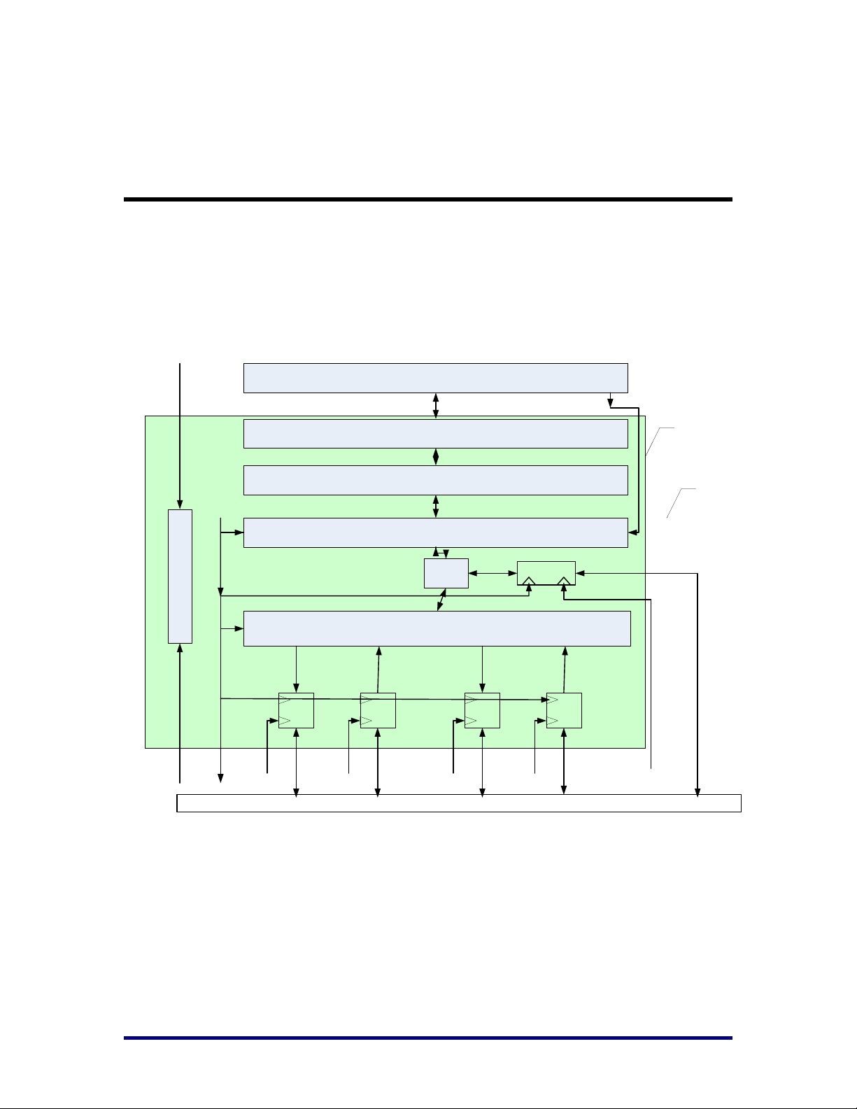
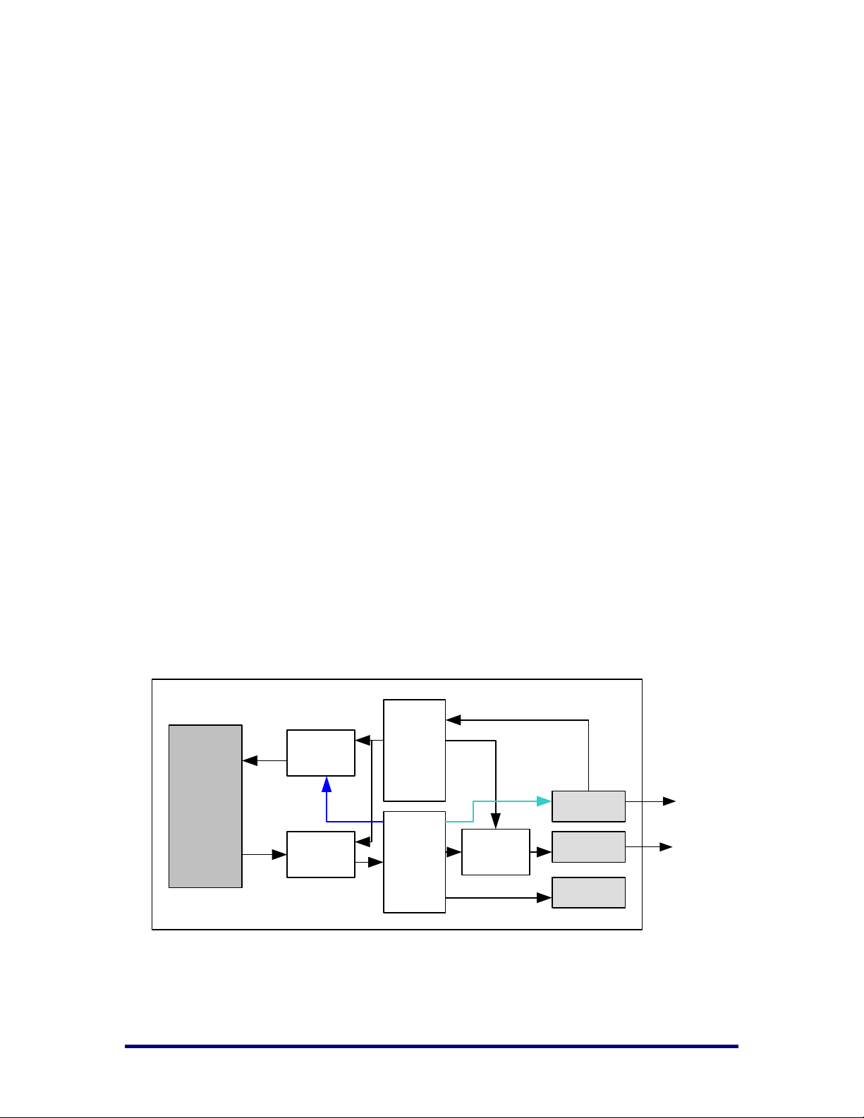
The PCI Express (PCIe) standard can be implemented in the Achronix22i device. Figure 1 shows
a block diagram of the PCIe hard IP with the DMA core for high-speed data transfer to/from the
user fabric. Figure 2 shows the DMA’s major interfaces, which will be discussed later.
Figure 1: PCIe with DMA Block Diagram
UG030, April 26, 2013
Page 9
9
DMA
Core
AXI Master
Interface
AXI Target
Interface
AXI DMA C2S
Interface
AXI DMA S2C
Interface
Figure 2: DMA Block Diagram
UG030, April 26, 2013
Page 10
10
Major Interfaces
clk
target_aclk
RX
TX
PCIe-Core Target Controller (Fabric Core)
SDRAM
Controller
Internal
Registers
Internal
SRAM
Target
Control
SDRAM
GPI/O
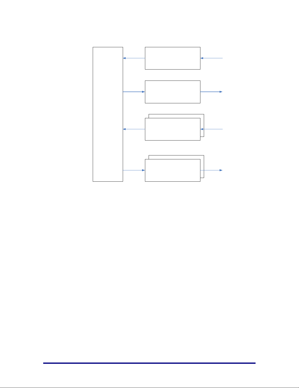
AXI Target Interface
The AXI Target Interface implements AXI3/AXI4 Master Protocol. Write and
read requests received via PCI Express (from remote PCI Express masters)
that target AXI regions of enabled Base Address or Expansion ROM regions
are forwarded to the AXI Target Interface for completion. Accesses to
registers inside the AXI DMA Back-End Core are handled by the core and do
not appear on the AXI Target Interface.
Figure 3 shows the interface connection between AXI Target Interface and
Fabric Controller:
Figure 3: AXI Target Interface
The design in Figure 3 enables another PCI Express master device (such as a
CPU) to access external SDRAM, internal SRAM, and General Purpose I/O.
In this design each of the three interfaces is assigned a memory Base Address
Register. The Target Control module steers the incoming packets from PCIeCore to the appropriate destination based upon the Base Address Register
that was hit and formats the data (if needed) to the appropriate width. The
design receives Posted Request packets containing write requests and data
and performs the writes on the addressed interface. The design receives
Non-Posted Request packets containing read requests, performs the read on
the addresses interface, and then transmits one or more Completion packets
containing the requested read data.
The AXI Target Interface implements write-read ordering to maintain
coherency for PCI Express transactions (see Figure 4).
UG030, April 26, 2013
Page 11

11
Ordering is maintained separately for internal DMA Register and AXI
destinations
The completion of a read request to the same destination (DMA
Registers or AXI) can be used to guarantee that prior writes to the
same destination have completed
Reads are blocked until all writes occurring before the read have fully
completed; for AXI, a write is completed when it returns a completion
response on the Write Response Channel; for internal DMA Registers,
a write is completed when it is written into the DMA Registers such
that a following read will return the new value
Supports full duplex bandwidth utilization when being driven by a
remote PCI Express DMA Master
Supports multiple simultaneously outstanding write and read requests
Utilizes maximum 16 beat bursts for compatibility with AXI3
and AXI4
UG030, April 26, 2013
Page 12
12
0
31ff 8000
2
4
0
0
0000 0000 0000 0000 0000 0000 0000 0000
t_areset_n
St1
t_aclk
St1
t_awvalid
St0
St1
t_awready
3'h0
t_awregion[2:0]
t_awaddr[31:0]
4'h0
t_awlen[3:0]
3'h4
t_awsize[2:0]
St0
t_wvalid
St0
t_wready
t_wdata[127:0]
t_wstrb[15:0]
St1
t_wlast
St0
t_bvalid
St1
t_bready
2'h0
t_bresp[1:0]
St0
t_arvalid
St0
t_arready
3'h0
t_arregion[2:0]
t_araddr[31:0]
4'h0
t_arlen[3:0]
3'h4
t_arsize[2:0]
St0
t_rvalid
St1
t_rready
t_rdata[127:0]
2'h0
t_rresp[1:0]
St1
t_rlast
0
000 0000 0000 0000 0000
31ff 8080
*0
...
...
...
...
...
...
...
...
...
...
...
...
...
...
...
...
...
...
...
...
...
...
...
...
...
...
...
000f f000
* 0002 0000 0000
* 8080 31ff 8084 31ff 8088 31ff 808c
* aea1 0001 000000 0000 0000
00
0
4
0
4
0
0
4
0
00f0
0007 0006 0000 0000 0000 1a2ab733
0000
0000 0000 0000
...
...
...
...
...
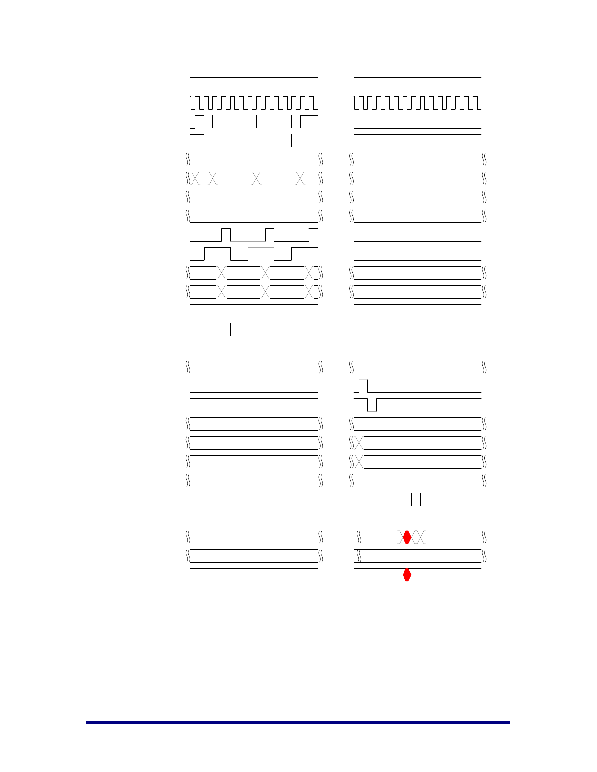
Figure 4: Timing Diagram for Target Interface
Moreover, the AXI Target Interface implements FIFOs to buffer multiple
writes and reads simultaneously to enable maximum bandwidth.
The AXI Target Interface implements a dual clock interface. The AXI clock
domain may be different than the PCI Express clock domain. Gray Code
UG030, April 26, 2013
Page 13

13
synchronization techniques can be used to enable support for a wide variety
of AXI clock rates.
User’s Task: It is important to consume target write and read transactions
relatively quickly as it is possible to stall PCI Express completions (used for
S2C DMA for example) if target write and read transactions are allowed to
languish in the PCI Express Core Receive Buffer.
Target Only Design
The Target-Only design is the simplest design to implement and works well
if the master device transmits packets with larger burst widths. Throughput
in PCI Express (and in its predecessors PCI and PCI-X) is directly
proportional to burst size, so small transaction burst sizes result in low
throughput.
User’s Task: To fix the inherent limitations of CPU and other small burst
size masters, a design must be able to master the PCI Express bus and enact
transactions with larger burst sizes (see the AXI Master Interface section for
additional details).
Still, the Target-Only design is ideal, due to its simplicity and hence smaller
design size, for lower bandwidth applications and applications where
another master is available to master transactions at larger burst sizes.
System software is also easier to write for target-only applications since only
basic CPU move instructions need to be used and the software complexities
of a DMA-based system (interrupts, DMA system memory allocation, etc.)
do not need to be handled.
AXI Back-End DMA Interface
The AXI DMA Interface is the mechanism through which user logic interacts
with the DMA Engine. The AXI DMA Interface orchestrates the flow of DMA
data between user logic and PCI Express.
The AXI DMA System to Card and AXI DMA Card to System interfaces
support multiple AXI protocol options (which are selected with the DMA
Back End DMA Engine inputs c2s/s2c_fifo_addr_n):
AXI3/AXI4
AXI4-Stream
Addressable FIFO DMA
When a DMA Engine is configured to implement an AXI3/AXI4 interface,
system software can set the “Addressable FIFO DMA” Descriptor bit in all
Descriptors of an application DMA transfer to instruct the DMA Back End to
provide the same starting AXI address provided by software for all AXI
UG030, April 26, 2013
Page 14
14
transactions for this packet. This allows the user hardware design to
c2s_areset_n[1:0]
2'h3
c2s_aclk[1:0]
2'h0
c2s_fifo_addr_n[1:0]
2'h3
c2s_arvalid[1:0]
2'h0
c2s_arready[1:0]
2'h3
c2s_araddr[71:0]
c2s_arlen[7:0]
8'h00
c2s_arsize[5:0]
6'h24
c2s_rvalid[1:0]
2'h0
c2s_rready[1:0]
2'h3
c2s_rdata[255:0]
c2s_rresp[3:0]
4'h0
c2s_rlast[1:0]
2'h0
c2s_ruserafull[1:0]
2'h0
c2s_ruserstrb[31:0]
3 0
*3*3 *3*3*3
0
000 b000 0000
2 0
0
2
0
0
2
2
0
f5
0
3
*3*3 *3 *3
*3*3*f3 *3
3
0
0000 0000
0 3
*4 *5*3 *3
2
0
* 0000 2400
2 0
2 0 2
...
...
...
...
...
...
...
...
...
...
...
...
...
...
...
...
...
...
...
...
...
...
...
...
...
...
...
...
...
...
3 3 3
0 2
0
00 0000 9000 0000 2400 00 0000 a000 0000 2400
15 f5
24 24
f5
24
0
0
2 2 2 2 2
0 0 0
3 3
00000
0 0
0000 0000 0000 0000
0
2
0
00 0000 a000 0000 240000 0000 9000 0000 2400
6665
*3
...
...
...
implement FIFOs for some AXI DMA transactions while simultaneously also
supporting addressable RAM for other AXI DMA transactions.
Figure 5 depicts the Card-to-System DMA interface and
Figure 6 the System-to-Card DMA interface.
UG030, April 26, 2013
Figure 5: Timing Diagram for Card-to-System DMA Interface
Page 15
15
2'h0s2c_aclk[1:0]
St0s2c_aclk[1]
St0s2c_aclk[0]
2'h3s2c_fifo_addr_n[1:0]
2'h0s2c_awvalid[1:0]
St0s2c_awvalid[1]
St0s2c_awvalid[0]
2'h3s2c_awready[1:0]
s2c_awready[71:0]
8'h0fs2c_awlen[7:0]
2'h0s2c_awusereop[1:0]
6'h24s2c_awsize[5:0]
s2c_wdstrb[31:0]
2'h0s2c_wlast[1:0]
2'h0s2c_wusereop[1:0]
2'h0s2c_bvalid[1:0]
2'h3s2c_bready[1:0]
4'h0s2c_bresp[3:0]
...
...
...
...
...
...
...
...
...
...
...
...
...
...
...
...
...
...
...
...
...
...
...
...
...
...
...
...
...
...
...
...
...
...
...
...
...
...
...
...
...
...
...
...
s2c_areset_n[1:0] 2'h3
s2c_wdata[255:0]
s2c_wready[1:0]
2'h3
s2c_wvalid[1:0] 2'h1
*fc
7b00 00 0000
*3c
3
3
3
0f
0
24
1
3
0000 ffff
0
0
0
0
3
00 0000 0000
3 3
3 3
0 0 0 0 0
0001 7c00 00 0000 0000 0001 7d00 00 0000 0000 0001 7d00
0f 0f
0
24
0
24
1 0
3 3
0000 ffff
0
0
0
0
3
0000 ffff
0
0
0
0
3
111
...
...
...
Figure 6: Timing Diagram for System-to-Card DMA Interface
Packet DMA Descriptor Format
A 256-bit (32-byte) Descriptor is defined for Packet DMA which contains the
Control fields required to specify a packet copy operation and the Status
fields required to specify the success/failure of the packet copy operation.
The Descriptor is split into Control and Status fields:
Control fields are fields that are written into the Descriptor by
software before the Descriptor is passed to the DMA Engine. Control
fields specify to the DMA Engine what copy operation to perform.
Status fields are fields that are written into the Descriptor by the
DMA Engine after completing the DMA operation described in the
UG030, April 26, 2013
Page 16

16
Control portion of the Descriptor. Status fields indicate to software
Data Flow
Direction
256-Bit Field (addresses increment left and down)
Card-to-
System
{C2SDescStatusFlags[7:0], Reserved[3:0],
C2SDescByteCount[19:0], C2SDescUserStatus[31:0],
C2SDescUserStatus[63:32], DescCardAddr[31:0],
C2SDescControlFlags[7:0], DescCardAddr[35:32],
DescByteCount[19:0], DescSystemAddr[31:0],
DescSystemAddr[63:32], DescNextDescPtr[31:5],
5’b00000}
System-to-
Card
{S2CDescStatusFlags[7:0],
S2CDescStatusErrorFlags[3:0],
S2CDescByteCount[19:0], S2CDescUserControl[31:0],
S2CDescUserControl[63:32], DescCardAddr[31:0],
S2CDescControlFlags[7:0], DescCardAddr[35:32],
DescByteCount[19:0], DescSystemAddr[31:0],
DescSystemAddr[63:32], DescNextDescPtr[31:5],
5’b00000}
the Descriptor completion status. Software should zero all status
fields prior to making the Descriptor available to the DMA Engine.
To promote ease of re-using Descriptors (for circular queues),
Control and Status fields are assigned their own locations in the
Descriptor.
Table 1 described the Packet DMA Descriptor format.
Table 1: Packet DMA Descriptor Format
Card-to-System Descriptor Field Descriptors
Data flow for Card-to-System DMA is from the user design to system
memory. The DMA Engine receives packets on its DMA Interface from the
user hardware design and writes the packets into system memory at the
locations specified by the Descriptors. The Packet DMA Engine assumes that
the packet sizes are variable and unknown in advance. The Descriptor Status
fields contain the necessary information for software to be able to determine
the received packet size and which Descriptors contain the packet data.
Packet start and end are indicated by the SOP and EOP C2SDescStatusFlag
bits. A packet may span multiple Descriptors. SOP=1, EOP=0 is a packet start,
SOP=EOP=0 is a packet continuation, SOP=0, EOP=1 is a packet end, and
SOP=EOP=1 is a packet starting and ending in the same Descriptor. The
received packet size is the sum of the C2SDescByteCount fields for all
Descriptors that are part of a packet.
UG030, April 26, 2013
Descriptor fields specific to Card-to-System DMA:
Page 17

17
C2SDescControlFlags[7:0] – Control
• Bit 7 – SOP – Set if this Descriptor contains the start of a
packet; clear otherwise; only set for addressable Packet
DMA
• Bit 6 – EOP – Set if this Descriptor contains the end of a
packet; clear otherwise; only set for addressable Packet
DMA
• Bits[5:3] – Reserved
• Bit[2] – Addressable FIFO DMA – If set to 1, the DMA Back-
End will use the same Card Starting Address for all DMA
Interface transactions for this Descriptor; this bit must be set
the same for all Descriptors that are part of the same packet
transfer; Addressable FIFO AXI addresses must be chosen
by the user design such that they are aligned to AXI max
burst size * AXI data width address boundaries; For
example: 16 * 16 == 256 bytes (addr[7:0] == 0x00) for AXI3
max burst size == 16 and AXI_DATA_WIDTH == 128-bits ==
16 bytes
• Bit[1] – IRQOnError – Set to generate an interrupt when this
Descriptor Completes with error; clear to not generate an
interrupt when this Descriptor Completes with error
• Bit[0] – IRQOnCompletion – Set to generate an interrupt
when this Descriptor Completes without error; clear to not
generate an interrupt when this Descriptor Completes
without error
C2SDescStatusFlags[7:0] – Status
• Bit 7 – SOP – Set if this Descriptor contains the start of a
packet; clear otherwise
• Bit 6 – EOP – Set if this Descriptor contains the end of a
packet; clear otherwise
• Bits[5] – Reserved
• Bit 4 – Error – Set when the Descriptor completes due to an
error; clear otherwise
• Bit 3 – C2SDescUserStatusHighIsZero – Set if
C2SDescUserStatus[63:32] == 0; clear otherwise
• Bit 2 – C2SDescUserStatusLowIsZero – Set if
C2SDescUserStatus[31:0] == 0; clear otherwise
• Bit 1 – Short – Set when the Descriptor completed with a
byte count less than the requested byte count; clear
otherwise; this is normal for C2S Packet DMA for packets
containing EOP since only the portion of the final Descriptor
required to hold the packet is used.
• Bit 0 – Complete – Set when the Descriptor completes
without an error; clear otherwise
C2SDescByteCount[19:0] - Status
• The number of bytes that the DMA Engine wrote into the
Descriptor. If EOP=0, then C2SDescByteCount will be the
same as the Descriptor size DescByteCount. If EOP=1 and
UG030, April 26, 2013
Page 18

18
the packet ended before filling the entire Descriptor, then
C2SDescByteCount will be less than the Descriptor size
DescByteCount. The received packet size is the sum of the
C2SDescByteCount fields for all Descriptors that are part of
a packet.
• C2SDescByteCount is 20-bits so supports Descriptors up to
2^20-1 bytes. Note that since packets can span multiple
Descriptors, packets may be significantly larger than the
Descriptor size limit.
C2SDescUserStatus[63:0] – Status
• Contains application specific status received from the user
when receiving the final data byte for the packet;
C2SDescUserStatus is only valid if EOP is asserted in
C2SDescStatusFlags. C2SDescUserStatus is not used by the
DMA Engine and is purely for application specific needs to
communicate information between the user hardware
design and system software. Example usage includes
communicating a hardware calculated packet CRC,
communicating whether the packet is an Odd/Even video
frame, etc. Use of C2SDescUserStatus is optional.
• C2SDescUserStatusHighIsZero and
C2SDescUserStatusLowIsZero are provided for ensuring
coherency of status information.
System-to-Card Descriptor Field Descriptors
Data flow for System-to-Card DMA is from system memory to the user
design. Software places packets into the Descriptors and then passes the
Descriptors to the DMA Engine for transmission. The DMA Engine reads the
packets from system memory and provides them to the user hardware
design on its DMA Interface. The software knows the packet sizes in advance
and writes this information into the Descriptors. Software sets SOP and EOP
S2CDescControlFlags during packet to Descriptor mapping to indicate
Packet start and end information. A packet may span multiple Descriptors.
SOP=1, EOP=0 is a packet start, SOP=EOP=0 is a packet continuation, SOP=0,
EOP=1 is a packet end, and SOP=EOP=1 is a packet starting and ending in
the same Descriptor. The transmitted packet size is the sum of all
S2CDescByteCount fields for all Descriptors that are part of a packet. The
Descriptor Status fields contain the necessary information for software to be
able to determine which Descriptors the DMA Engine has completed.
Descriptor fields specific to System-to-Card DMA:
S2CDescControlFlags[7:0] – Control
Bit 7 – SOP – Set if this Descriptor contains the start of a
packet; clear otherwise
Bit 6 – EOP – Set if this Descriptor contains the end of a
packet; clear otherwise
Bits[5:3] – Reserved
UG030, April 26, 2013
Page 19

19
Bit[2] – Addressable FIFO DMA – If set to 1, the DMA Back-
End will use the same Card Starting Address for all DMA
Interface transactions for this Descriptor; this bit must be set
the same for all Descriptors that are part of the same packet
transfer; Addressable FIFO AXI addresses must be chosen
by the user design such that they are aligned to AXI max
burst size * AXI data width address boundaries; For
example: 16 * 16 == 256 bytes for AXI3 max burst size == 16
and AXI_DATA_WIDTH == 128-bits == 16 bytes
Bit[1] – IRQOnError – Set to generate an interrupt when this
Descriptor Completes with error; clear to not generate an
interrupt when this Descriptor Completes with error
Bit[0] – IRQOnCompletion – Set to generate an interrupt
when this Descriptor Completes without error; clear to not
generate an interrupt when this Descriptor Completes
without error
S2CDescStatusFlags[7:0] - Status
• Bits[7:5] – Reserved
• Bit 4 – Error – Set when the Descriptor completes due to an
error; clear otherwise
• Bits[3:2] - Reserved
• Bit 1 – Short – Set when the Descriptor completed with a
byte count less than the requested byte count; clear
otherwise; this is generally an error for S2C Packet DMA
since packets are normally not truncated by the user design.
• Bit 0 – Complete – Set when the Descriptor completes
without an error; clear otherwise
S2CDescStatusErrorFlags[3:0] – Status – Additional information as
to why S2CDescStatusFlags[4] == Error is set. If
S2CDescStatusFlags[4] == Error is set then one or more of the
following bits will be set to indicate the additional error source
information.
• Bit 3 – Reserved
• Bit 2 – Set when received one or more DMA read data
completions with ECRC Errors
• Bit 1 – Set when received one or more DMA read data
completions marked as Poisoned (EP == 1)
• Bit 0 – Set when received one or more DMA read data
completions with Unsuccessful Completion Status
S2CDescUserControl[63:0] – Control
• Contains application specific control information to pass
from software to the user hardware design; the DMA Engine
provides the value of S2CDescUserControl to the user
design the same clock that SOP is provided.
S2CDescUserControl is not used by the DMA Engine and is
purely for application specific needs. Use of
S2CDescUserControl is optional.
S2CDescByteCount[19:0] – Control & Status
UG030, April 26, 2013
Page 20

20
• Control - During packet to Descriptor mapping, software
• Status – After completing a DMA operation, the DMA
• Note: S2CDescByteCount is 20-bits so supports Descriptors
AXI Master Interface
writes the number of bytes that it wrote into the Descriptor
into S2CDescByteCount. If EOP=0, then S2CDescByteCount
must be the same as the Descriptor size DescByteCount. If
EOP=1 and the packet ends before filling the entire
Descriptor, then S2CDescByteCount is less than the
Descriptor size DescByteCount. The transmitted packet size
is the sum of the S2CDescByteCount fields for all
Descriptors that are part of a packet
Engine writes the number of bytes transferred for the
Descriptor into S2CDescByteCount. Except for error
conditions, S2CDescByteCount should be the same as
originally provided.
up to 2^20-1 bytes. Note that since packets can span multiple
Descriptors, packets may be significantly larger than the
Descriptor size limit.
The AXI Master Interface is an AXI4-Lite Slave interface that enables the user
to:
Generate PCI Express requests with up to 1 DWORD (32-bit)
payload
Write and read DMA Back-End internal registers to start DMA
operation and obtain interrupt status
The AXI Master Interface implements a register set to enable the
above functions.
A PCI Express request is carried out by writing the PCI Express-
specific information (PCI Express Address, Format and Type, etc.) to
the register set and then writing to another register to execute the
request.
DMA Registers are made accessible via AXI reads and writes
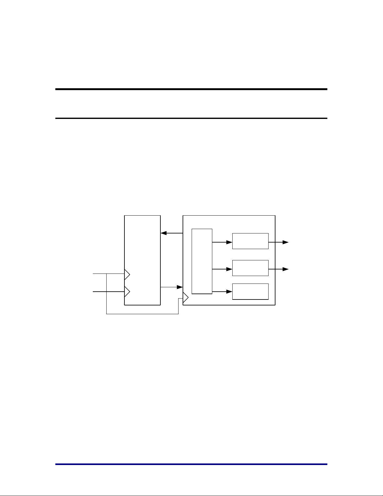
The design in Figure 7 contains the same elements as the Target-Only
design described in section AXI Target Interface, but is enhanced with Direct
Memory Access (DMA) capability to achieve greater throughput. For the
transfer of large volumes of data, the DMA has inherently better throughput
than target-only designs both because the burst sizes are generally much
larger, but also because DMA read transactions can be cascaded while most
software using CPU move instructions will block on a read until it
UG030, April 26, 2013
Page 21
21
completes. Writes perform reasonably well in either case since writes are
PCIe-Core
Arbiter
Arbiter
TX
RX
DMA
Control
Target
Control
Arbiter
Internal
Registers
SDRAM
Cntrl
Internal
SRAM
GPIO
SDRAM
Speedster22i
always posted and software will generally not block on write transactions.
In the Target with Master DMA design each of the three interfaces (external
SDRAM, internal SRAM, and DMA registers/General Purpose I/O) are
assigned a memory Base Address Register. The Target Control module steers
the incoming packets to the appropriate destination based upon the Base
Address Register that was hit and formats the data (if needed) to the
appropriate width.
As a target, the design receives Posted Request packets containing write
requests and data and performs the writes on the addressed interface. The
design receives Non-Posted Request packets containing read requests,
performs the read on the addresses interface, and then transmits one or more
Completion packets containing the requested read data.
The DMA Control module masters transactions on the PCI Express bus (it
generates requests, rather than just responding to requests). System software
controls the DMA transactions via target writes and reads to the Internal
Registers.
As a master, the design transmits Posted (write request + data) and NonPosted (read request) requests and monitors the RX bus for (reads only) the
corresponding Completion packets containing the transaction status/data.
Since the SDRAM Controller module must be shared, an SDRAM Arbiter is
required to arbitrate between servicing DMA and target SDRAM accesses.
Since there are two modules that need access to the Transmit and Receive
Interfaces, arbiters are required.
The Target with Master DMA design is well suited to applications that need
to move a lot of data at very high throughput rates. The higher throughput
comes at a price however. Design complexity is significantly greater than a
target-only design and system software is more complicated to write.
UG030, April 26, 2013
Figure 7: AXI Target with Master DMA (Control Flow)
Page 22

22
DMA Bypass Interface
The bypass interface disables DMA backend, and communicates directly to
the PCI Express core. In its place, the user can build a soft DMA engine that
connects to this interface.
Transmit Interface
The Transmit Interface is the mechanism with which the user transmits PCIe
transaction-layer packets (TLPs) over the PCI Express bus. The user
formulates TLPs for transmission in the same format as defined in the PCI
Express Specification
User’s task: Supply a complete TLP comprised of packet header, data
payload, and optional TLP Digest.
The core Data Link Layer adds the necessary framing (STP/END), sequence
number, Link CRC (LCRC), and optionally ECRC (when ECRC support is
present and enabled).
Packets are transmitted to master write and read requests, to respond with
completions to target reads and target I/O requests, to transmit messages,
etc.
The Achronix PCIe Core automatically implements any necessary replays
due to transmission errors, etc. If the remote device does not have sufficient
space in its Receive Buffer for the packet, the core pauses packet transmission
until the issue is resolved.
PCI Express packets are transmitted exactly as received by the core on the
Transmit Interface with no validation that the packets are formulated
correctly by the user.
User’s task: It is critical that all packets transmitted are formed correctly and
that vc0_tx_eop is asserted at the appropriate last vc0_tx_data word in each
packet.
PCI Express Packets are integer multiples of 32-bits in length. Thus, 64-bit,
128-bit, and 256-bit Core Data Width cores may have an unused remainder
portion in the final data word of a packet. The core uses the packet TLP
header (Length, TLP Digest, and Format and Type) to detect whether the
packet has an unused remainder and will automatically discard and not
transmit the unused portion of the final data word.
The core contains transmit DLLP-DLLP, TLP-TLP, and TLP-DLLP packing to
maximize link bandwidth by eliminating, whenever possible, idle cycles left
by user TLP transmissions that end without using the full Core Data Width
word.
The Transmit Interface includes the option to nullify TLPs (instruct Receiver
to discard the TLP) to support cut-through routing and the user being able to
cancel TLP transmissions when errors are detected after the TLP
transmission has started. Nullified TLPs that target internal core resources
(Root Port & Downstream Switch Port Configuration Registers and Power
Management Messages) are discarded without affecting the internal core
resources.
UG030, April 26, 2013
Page 23

23
Receive Interface
The Receive Interface is the mechanism with which the user receives PCIe
packets from the PCIe bus. Packets are received and presented on the
interface in the same format defined in the PCI Express Specification; the
user receives complete Transaction Layer packets comprised of packet
header, data payload, and optional TLP Digest. The core automatically
checks packets for errors, requests replay of packets as required, and strips
the Physical Layer framing and Data Link Layer sequence number, and Link
CRC (LCRC) before presenting the packet to the user.
The core decodes received TLPs and provides useful transaction attributes
such that the packet can be directed to the appropriate destination without
the need for the user to parse the packet until its destination. If the packet is
an I/O or Memory write or read request, the base address register resource
that was hit is indicated. If the packet is a completion, the packet’s tag field is
provided. The core also provides additional useful transaction attributes.
Packets that appear on the Receive Interface have passed the Sequence
Number, Link CRC, and malformed TLP checks required by the PCI Express
Specification.
UG030, April 26, 2013
Page 24
24
Port List
Pin Name
Direction
Clock
Description
pcie_refclk_p[7:0]
Input
Reference Clock Input
pcie_refclk_n[7:0]
Input
Reference Clock Input
tx_p[7:0]
Output
Serial Transmit
tx_n[7:0]
Output
Serial Transmit
rx_p[7:0]
Input
Serial Receive
rx_n[7:0]
Input
Serial Receive
i_serdes_sbus_req [7:0]
Input
i_sbus_clk
SerDes side SBUS request
i_serdes_sbus_data [15:0]
Input
i_sbus_clk
SerDes side SBUS data to write
o_serdes_sbus_data [15:0]
Output
i_sbus_clk
SerDes side SBUS data to read
o_serdes_sbus_ack [7:0]
Output
i_sbus_clk
SerDes side SBUS
acknowledgement
SerDes Interface
Table 2: SerDes Interface Pin Descriptions
UG030, April 26, 2013
Page 25

25
Fabric-Side Interface
Port Name
Direction
Clock
Description
perst_n
Input
user_clk
Fundamental Reset; active-low asynchronous
assert, synchronous de-assert; resets the entire
core except for Configuration Registers which
are defined by PCI Express to be unaffected by
fundamental reset; on rst_n de-assertion the
core starts in the Detect Quiet Link Training
and Status State Machine (LTSSM) state with
the Physical Layer down (mgmt_pl_link_up_o
== 0) and Data Link Layer down
(mgmt_dl_link_up_o == 0).
clk_out
Output
core_clk
Core clock; all core ports are synchronous to
the rising edge of clk_out.
The PIPE Specification defines two possible
approaches to adapting to changes in the line
rate of PCI Express (changing between 2.5, 5,
and 8GT/s operation). The core natively
supports PHY that implement the PIPE
constant-data-width, variable-clock-frequency
PIPE interface and PHY that implement the
PIPE variable-data-width, constant-clockfrequency PIPE interface.
The frequency of clk_out must be the fullbandwidth frequency for the PHY per-lane
data width (Core Data Width/Max Lane
Width; which is static for a given core
configuration) and the current line rate:
16-bit Per-Lane Data Width core
configurations:
8.0 GT/s -> 500 MHz
5.0 GT/s -> 250 MHz
2.5 GT/s -> 125 MHz
clk_out is connected to the PHY’s clk_out, or a
binary multiple/divisor of clk_out when PHY
and Core have different data widths.
Note: Per PCI Express Specification, PHYs
must use the same clock reference as the
remote PCIe device to be compatible with
systems implementing Spread Spectrum
Table 3: Fabric-Side Port Descriptions
UG030, April 26, 2013
Page 26

26
Port Name
Direction
Clock
Description
clocking (majority of open systems). The
required 600 ppm maximum clock difference
between devices may not be met when Spread
Spectrum clocking is in use unless both devices
in the link are using the same Spread
Spectrum-modulated clock reference.
i_sbus_clk
Input
i_sbus_clk
Serial-Bus clock
i_sbus_req
Input
i_sbus_clk
SBUS interface request
i_sbus_sw_rst
Input
i_sbus_clk
Soft reset to the SBUS interface
i_sbus_data[1:0]
Input
i_sbus_clk
SBUS write data
o_sbus_ack
Output
i_sbus_clk
SBUS acknowledgment
o_sbus_rdata[1:0]
Output
i_sbus_clk
SBUS read data
bypass_clk
Input
bypass_clk
DMA Bypass clock
bypass_rst_n
Input
bypass_clk
DMA Bypass Reset
bypass_tx_valid
Input
bypass_clk
DMA Bypass Tx Data Valid
bypass_tx_ready
Output
bypass_clk
DMA Bypass Tx ready
bypass_tx_almost_full
Output
bypass_clk
DMA Bypass Tx Data Fifo almost full
bypass_tx_sop
Input
bypass_clk
Start of packet indicator and packet transmit
request; set == 1 coincident with the first
vc0_tx_data word in each packet. vc0_tx_sop
may not be asserted until the user is ready to
provide the entire packet with the minimum
possible timing of the core’s vc0_tx_en
assertions.
The user may wait state the transmit interface
only between packets; the user may choose to
hold off on transmitting a packet by not
asserting vc0_tx_sop.
bypass_tx_eop
Input
bypass_clk
End of packet indicator; set == 1 coincident
with the last vc0_tx_data word in each packet.
bypass_tx_data[127:0]
Input
bypass_clk
Packet data to transfer; vc0_tx_data must be
valid from the assertion of vc0_tx_sop until the
packet is fully consumed with the assertion of
vc0_tx_eop == vc0_tx_en == 1. The core may
assert and de-assert vc0_tx_en at any time, so
the user must ensure that vc0_tx_sop,
vc0_tx_eop, and vc0_tx_data are always valid.
Packet data must comprise a complete
Transaction Layer packet as defined by the PCI
Express Specification including the entire
packet header, data payload, and optional TLP
Digest (ECRC). The core adds the necessary
STP/END/EDB framing, Sequence Number,
LCRC, and for cores with ECRC support,
ECRC as part of its Data Link Layer
UG030, April 26, 2013
Page 27

27
Port Name
Direction
Clock
Description
functionality.
PCI Express Packets are integer multiples of
32-bits in length. Thus, 64-bit and 128-bit Core
Data Width cores may have an unused
remainder portion in the final data word of a
packet. The core uses the packet TLP header
(Length, TLP Digest, and Format and Type) to
detect whether the packet has an unused
remainder and will automatically discard and
not transmit the unused portion of the final
data word.
bypass_tx_data_valid[15:0]
Input
bypass_clk
DMA Bypass Tx Data Byte Valid
bypass_tx_np_ok
Output
bypass_clk
vc0_tx_np_ok indicates when the user is
allowed to transmit non-posted requests.
1: Non-Posted Requests are permitted
0: Non-Posted Requests are not permitted
If a non-posted request is transmitted when
there are no non-posted receive buffer credits
available in the remote PCI Express device,
then the core will be unable to send the nonposted request until credits are freed. If the
remote device is unable to free non-posted
credits until receiving a TLP from the core then
this leads to a deadlock condition that cannot
be resolved.
vc0_tx_np_ok is implemented to avoid this
condition by making it not possible for
transmissions to be stalled by the inability to
transmit non-posted requests. The core
implements a small non-posted request FIFO.
When non-posted requests cannot be accepted
by the remote device, this FIFO will fill, and
when it’s almost full threshold is hit,
vc0_tx_np_ok will de-assert (== 0) stopping the
user from being able to transmit additional
non-posted requests. Additional posted
requests and completions are not blocked by
vc0_tx_np_ok and continue to transmit if
credits are available in the remote Receive
Buffer. Per PCI Express transaction ordering
rules, Posted Requests and Completions must
be allowed to pass Non-Posted requests to
avoid deadlocks; Completions and Posted
Requests are not required to be able to pass
one another.
UG030, April 26, 2013
Page 28

28
Port Name
Direction
Clock
Description
User’s task: User logic must stop the
transmission of new Non-Posted requests
when vc0_tx_np_ok == 0. A non-posted packet
transmission that has already asserted
vc0_tx_sop must continue to be transmitted in
full. vc0_tx_np_ok should be used to stop new
assertions of vc0_tx_sop for non-posted
requests. Because vc0_tx_np_ok is an almost
full flag, it is allowed for vc0_tx_np_ok to be
used as the input to the register that generates
vc0_tx_sop for non-posted transactions
(vc0_tx_np_ok does not have to be used
combinatorial to mask vc0_tx_sop).
It is recommended for all user designs to use
vc0_tx_np_ok.
bypass_rx_valid
Output
bypass_clk
DMA Bypass Rx Data Valid
bypass_rx_ready
Input
bypass_clk
DMA Bypass Rx Ready
bypass_rx_data[127:0]
Output
bypass_clk
TLP data to receive; vc0_rx_data is valid from
the assertion of vc0_rx_sop until the packet is
fully consumed with the assertion of
vc0_rx_eop == vc0_rx_en == 1.
TLP data comprises a complete Transaction
Layer packet as defined by the PCI Express
Specification including the entire packet
header, data payload, and optional TLP Digest
(ECRC). The core strips the packet’s
STP/END/EDB framing, Sequence Number,
and Link CRC as part of its Data Link Layer
functionality prior to the TLP appearing on
this interface. The core checks TLP ECRC,
when present and when checking is enabled,
but does not remove the ECRC from the TLP.
PCI Express TLPs are integer multiples of 32bits in length. Thus, 64-bit and 128-bit Core
Data Width cores may have an unused
remainder portion in the final data word of a
packet. The user is responsible for detecting
and discarding any unused remainder at the
end of the TLP. All of the necessary
information to detect a remainder is located in
the packet TLP header (Length, TLP Digest,
and Format and Type) fields.
bypass_rx_data_valid[15:0]
Output
bypass_clk
DMA Bypass Rx Data Byte Valid
bypass_rx_sop
Output
bypass_clk
Start of TLP indicator and packet receive
request; set == 1 coincident with the first
vc0_rx_data word in each TLP. Once
UG030, April 26, 2013
Page 29

29
Port Name
Direction
Clock
Description
vc0_rx_sop is asserted, the user may assert
vc0_rx_en as desired to consume the TLP.
bypass_rx_eop
Output
bypass_clk
End of TLP indicator; set == 1 coincident with
the last vc0_rx_data word in each packet.
bypass_rx_ecrc_error
Output
bypass_clk
ECRC error indicator; set == 1 from vc0_rx_sop
to vc0_rx_eop inclusive for received TLPs
which contain a detected ECRC error. Clear ==
0 otherwise.
vc0_rx_err_ecrc only reports ECRC errors
when ECRC checking is enabled. ECRC
checking is enabled by software through the
AER Capability.
Packets with ECRC errors are presented on the
Receive Interface in the same format that they
are received including the TLP Digest (ECRC).
User’s task: The user design must decide how
to handle/recover from the error including
whether to use the TLP with the error. ECRC
errors need for higher level software to
correct/handle the error since it is unknown
where in the PCIe hierarchy the error occurred
and PCIe does not have a standard mechanism
for rebroadcasting packets end to end as it
does for a given PCIe link via the Link CRC.
bypass_rx_decode_info[12:0]
Output
bypass_clk
TLP type indicator; provides advance
information about the TLP to facilitate TLP
consumption; this port has a different meaning
in Root Port and Switch Modes.
The core decodes received TLP headers to
determine their destination; the core passes
this information to the Transaction Layer
Interface by asserting the appropriate bits in
this field. See the description of
mgmt_cfg_constants: Base Address Cfg[5:0]
sub fields in
Individual bits of vc0_rx_cmd_data[12:0] carry
the following meaning:
Bits[12:10] – Traffic Class of the packet
Bit[9] – Completion/Base Address
Region indicator
1: indicates the TLP is a Completion or
Message routed by ID
0: indicates the TLP is a read or write
request (or a Message routed by
address) targeting a Base Address
Region; the remaining bits in this field
UG030, April 26, 2013
Page 30

30
Port Name
Direction
Clock
Description
are decoded differently for
Completion versus Base Address
Region hits
Bits[8:0] –
o If Completion TLP (Bit[9] == 1)
Bits[8] - Reserved
Bits[7:0] – Tag; the
Requestor Tag
contained in the TLP;
use to route
completions to the
associated requestor
logic; this field is
reserved if the TLP is a
message rather than a
completion
o If Base Address Region TLP
(Bit[9] == 0)
Bit[8] – When (1), the
packet is a “write”
transaction; when (0),
the packet is a “read”
transaction
Bit[7] – When (1), the
packet requires one or
more Completion
transactions as a
response; (0)
otherwise
Bit[6] – (1) if the TLP
targets the Expansion
ROM Base Address
region
Bit[5] – (1) if the TLP
targets Base Address
Region 5
Bit[4] – (1) if the TLP
targets Base Address
Region 4
Bit[3] – (1) if the TLP
targets Base Address
Region 3
Bit[2] – (1) if the TLP
targets Base Address
Region 2
Bit[1] – (1) if the TLP
UG030, April 26, 2013
Page 31

31
Port Name
Direction
Clock
Description
targets Base Address
Region 1
Bit[0] – (1) if the TLP
targets Base Address
Region 0
vc0_rx_cmd_data is valid for the entire packet
(from vc0_rx_sop == 1 through vc0_rx_eop ==
vc0_rx_en == 1)
bypass_interrupt
Input
bypass_clk
mgmt_interrupt is used to generate interrupt
events on the PCI Express link.
Interrupt support is enabled by setting
mgmt_cfg_constants[128] (Interrupt Enable) ==
1.
The core contains the following two interrupt
configuration options:
Single Interrupt Configuration
o Support for 1 Legacy Interrupt
o Support for 1 MSI Interrupt
o mgmt_interrupt is used to
signal both Legacy and MSI
interrupts
Multiple Interrupt Configuration
o Support for 1 Legacy Interrupt
o Support for up to 32 MSI
Interrupts
o Support for up to 2048 MSI-X
Interrupts
o mgmt_interrupt is used to
signal only Legacy interrupts
o mgmt_interrupt_msix_req,
mgmt_interrupt_msix_ack and
mgmt_interrupt_msix_vector,
available only in this
configuration, are used to
signal MSI and MSI-X
interrupts.
System software selects MSI-X, MSI, or Legacy
Interrupt mode as part of the boot process by
writing MSI-X_Enable==1 or MSI_Enable ==1
or leaving both MSI-X_Enable and MSI_Enable
Configuration Registers at their default
disabled value.
The current interrupt mode of operation is
available by monitoring
mgmt_cfg_status[1296] (MSI_Enable) and
UG030, April 26, 2013
Page 32

32
Port Name
Direction
Clock
Description
mgmt_cfg_status[1183] (MSI-X Enable):
MSI-X_Enable==1 : MSI-X
Interrupt Mode
MSI_Enable ==1 : MSI Interrupt
Mode
MSI-X_Enable == 0 & MSI_Enable
== 0 : Legacy Interrupt Mode
Note: It is illegal for software to set both MSIX_Enable and MSI_Enable at the same time.
User’s task: User interrupt logic must behave
differently depending upon the value of MSIX_Enable and MSI_Enable and whether the
core is a Single or Multiple Interrupt
Configuration:
Single Interrupt Configuration
When Legacy Interrupt Mode is
enabled (MSI_Enable == 0),
mgmt_interrupt implements one levelsensitive interrupt (INTA, INTB,
INTC, or INTD as selected by
mgmt_cfg_constants[132:131]). All
interrupt sources should be logically
ORed together to generate
mgmt_interrupt. Each interrupt source
should continue to drive a 1 until it has
been serviced and cleared by software
at which time it should switch to
driving 0. The core monitors high and
low transitions on mgmt_interrupt and
sends an Interrupt Assert message on
each 0 to 1 transition and an Interrupt
De-Assert Message on each 1 to 0
transition. Transitions which occur too
close together to be independently
transmitted are merged.
When MSI Interrupt Mode is enabled
(MSI_Enable == 1), mgmt_interrupt is
used to implement one MSI Message.
An MSI Interrupt Message is
generated each time mgmt_interrupt
transitions from 0 to 1. To promote
sharing of mgmt_interrupt among
several interrupt sources, each source
should assert mgmt_interrupt for a
single clock cycle and all sources
UG030, April 26, 2013
Page 33

33
Port Name
Direction
Clock
Description
should be ORed together onto
mgmt_interrupt. 0 to 1 transition
events which occur too close together
to be independently transmitted are
merged together into one MSI
message.
Multiple Interrupt Configuration
When Legacy Interrupt Mode is
enabled (MSI-X_Enable == 0 &
MSI_Enable == 0), mgmt_interrupt
implements one level-sensitive
interrupt (INTA, INTB, INTC, or INTD
as selected by
mgmt_cfg_constants[132:131]). All
interrupt sources should be logically
ORed together to generate
mgmt_interrupt. Each interrupt source
should continue to drive a 1 until it has
been serviced and cleared by software
at which time it should switch to
driving 0. The core monitors high and
low transitions on mgmt_interrupt and
sends an Interrupt Assert message on
each 0 to 1 transition and an Interrupt
De-Assert Message on each 1 to 0
transition. Transitions which occur too
close together to be independently
transmitted are merged.
When MSI-X or MSI Interrupt Mode is
enabled (MSI-X_Enable == 1 or
MSI_Enable == 1), mgmt_interrupt is
not used and MSI-X/MSI interrupts are
signaled on mgmt_interrupt_msix_req,
mgmt_interrupt_msix_ack, and
mgmt_interrupt_msix_vector instead.
bypass_msi_en
Output
bypass_clk
MSI interrupt enable
bypass_msix_en
Output
bypass_clk
MSI-X interrupt enable
bypass_interrupt_msix_req
Input
bypass_clk
mgmt_interrupt_msix_req,
mgmt_interrupt_msix_ack, and
mgmt_interrupt_msix_vector are used to
signal MSI-X and MSI interrupts when the
MSI-X/Multi-Vector MSI Configuration core
option is present.
To request an MSI-X or MSI interrupt message
to be transmitted, mgmt_interrupt_msix_req is
UG030, April 26, 2013
Page 34

34
Port Name
Direction
Clock
Description
set to 1 and mgmt_interrupt_msix_vector
indicates the interrupt vector that is to be
transmitted. Once mgmt_interrupt_msix_req is
set, mgmt_interrupt_msix_req and
mgmt_interrupt_msix_vector must remain at
their same values until
mgmt_interrupt_msix_ack is asserted == 1
indicating that the requested interrupt message
was transmitted.
If MSI_En == 1, then the design is operating in
MSI interrupt mode. The core supports up to
the maximum of 32 interrupt vectors
supported by the MSI Capability. The interrupt
vector number to transmit is placed on
mgmt_interrupt_msix_vector[4:0] and
mgmt_interrupt_msix_vector[127:5] is set to all
zeros. The core transmits MSI Interrupts by
transmitting a Memory Write containing the
address and data value (with lower data bits
modified to signal the vector number) setup by
software in the MSI Capability. System
software may not allocate as many MSI
interrupt vectors as requested by the design so
user hardware and software must be designed
to share interrupts if required. The core
performs the necessary aliasing (dropping the
higher mgmt_interrupt_msix_vector[4:0] bits
as required) so the user may drive a full 5-bit
vector number even if fewer vectors are
assigned.
If MSI-X_En == 1, then the design is operating
in MSI-X interrupt mode. The core supports up
to the maximum of 2048 interrupt vectors
supported by the MSI-X Capability.
User’s task: In MSI-X Interrupt mode, the user
implements the required MSI-X Table and
MSI-X PBA in memory space mapped by a
Base Address Register. Each Table entry/vector
consists of a 64-bit address, 32-bit data value,
and 32-bit vector control word. To request an
interrupt be transmitted, the MSI-X Table entry
corresponding to the desired vector number is
fetched and placed onto
mgmt_interrupt_msix_vector[127:0] and
mgmt_interrupt_msix_req is set == 1. If the
interrupt is masked by the MSI-X Capability
UG030, April 26, 2013
Page 35

35
Port Name
Direction
Clock
Description
global Function Mask (mgmt_cfg_status[1182])
or by the per vector Mask Bit (MSI-X Table
entry bit 96) then that vector is masked and
cannot be requested by asserting
mgmt_interrupt_msix_req until the vector is
unmasked. For each clock cycle that
mgmt_interrupt_msix_req == 1 and
mgmt_interrupt_msix_ack ==1, the core
transmits a MSI-X Interrupt by transmitting a
Memory Write containing the address and
data value contained in the provided
mgmt_interrupt_msix_vector[127:0]. System
software may not allocate as many MSI-X
interrupt vectors as requested by the design so
user hardware and software must be designed
to share interrupts if required. The user
hardware design must take into account any
interrupt sharing and always provide a valid,
system-software-allocated vector.
bypass_interrupt_msix_ack
Output
bypass_clk
bypass_interrupt_msix_vector
[127:0]
Input
bypass_clk
bypass_enable
Input
bypass_clk
DMA Bypass interface enable
UG030, April 26, 2013
Page 36

36
DMA-Side Port Descriptions
Pin Name
Direction
Clock
Description
t_areset_n
Input
t_aclk
Active-low asynchronous assert, t_aclk-synchronous
de-assert reset;
Must be asserted when DMA Back End PCI Express
reset is asserted.
t_aclk
Input
AXI interface clock; may be a different clock than the
clock used on the PCI Express-side of the AXI DMA
Back-End Core; synchronization techniques are used
to enable support for a wide variety of clock rates
t_awvalid
Output
t_aclk
Write Address Channel; Optional AWBURST,
AWLOCK, AWCACHE, AWPROT are not
implemented; AWBURST is always incrementingaddress burst; cache, protected, and exclusive
accesses not supported; see below for t_awregion
information
t_awready
Input
t_aclk
t_awregion
[2:0]
Output
t_aclk
t_awaddr
[31:0]
Output
t_aclk
t_awlen
[3:0]
Output
t_aclk
t_awsize
[2:0]
Output
t_aclk
t_wvalid
Output
t_aclk
Write Data Channel
t_wready
Input
t_aclk
t_wdata
[127:0]
Output
t_aclk
t_wstrb
[15:0]
Output
t_aclk
t_wlast
Output
t_aclk
t_bvalid
Input
t_aclk
Write Response Channel; space is reserved in the
master to receive response from all outstanding
write requests, so t_bready is always 1 and does not
need to be used.
t_bready
Output
t_aclk
t_bresp
[1:0]
Input
t_aclk
t_arvalid
Output
t_aclk
Read Address Channel; Optional ARBURST,
ARLOCK, ARCACHE, ARPROT are not
implemented; ARBURST is always incrementingaddress burst; cache, protected, and exclusive
accesses not supported; see below for t_arregion
information .
t_arready
Input
t_aclk
t_arregion
[2:0]
Output
t_aclk
t_araddr
[31:0]
Output
t_aclk
AXI Target Interface
Table 4: Target Interface Pin Descriptions
UG030, April 26, 2013
Page 37

37
Pin Name
Direction
Clock
Description
t_arlen
[3:0]
Output
t_aclk
target_awregion and target_arregion indicate PCI
Express Base Address Region hit information:
• 0: BAR0
• 1: BAR1
• 2: BAR2
• 3: BAR3
• 4: BAR4
• 5: BAR5
• 6: Expansion ROM
• 7: Reserved
t_arsize
[2:0]
Output
t_aclk
t_rvalid
Input
t_aclk
Read Data Channel; space is reserved in the master
to receive data from all outstanding read requests,
so t_rready is always 1
t_rready
Output
t_aclk
t_rdata
[127:0]
Input
t_aclk
t_rresp
[1:0]
Input
t_aclk
t_rlast
Input
t_aclk
Pin Name
Direction
Clock
Description
m_areset_n
Input
m_aclk
Active-low asynchronous assert, m_aclksynchronous de-assert reset
m_aclk
Input
AXI interface clock; may be a different clock than
the clock used on the PCI Express-side of the AXI
DMA Back-End Core; synchronization techniques
are used to enable support for a wide variety of
clock rates
m_awvalid
Input
m_aclk
A Write Address Channel transfer occurs when
m_awvalid == 1 and m_awready == 1
implemented
m_awready
Output
m_aclk
m_awaddr[15:0]
Input
m_aclk
Byte address of register to write
m_wdata [31:0]
Input
m_aclk
Data to write
m_wstrb [3:0]
Input
m_aclk
Byte enables for write
m_wvalid
Input
m_aclk
A Write Data Channel transfer occurs when
m_wvalid == 1 and m_wready == 1
m_wready
Output
m_aclk
m_bvalid
Output
m_aclk
A Write Response Channel transfer occurs when
m_bvalid == 1 and m_bready == 1
m_bready
Input
m_aclk
m_bresp [1:0]
Output
m_aclk
Status of write request: 0 – Successful; 1, 2,3 Error
m_araddr [15:0]
Input
m_aclk
Byte address of register to read
m_rvalid
Output
m_aclk
A Read Response Channel transfer occurs when
AXI Master Interface
Table 5: Master Interface Pin Descriptions
UG030, April 26, 2013
Page 38

38
Pin Name
Direction
Clock
Description
m_rready
Input
m_aclk
m_rvalid == 1 and m_rready == 1
m_rdata [31:0]
Output
m_aclk
Data read
m_rresp [1:0]
Output
m_aclk
Status of read request: 0 – Successful; 1, 2,3 Error
m_interrupt
[4:0]
Output
m_aclk
Pin Name
Direction
Clock
Description
s2c_areset_n
Output
s2c_aclk
Active-low asynchronous assert, s2c_aclk synchronous
de-assert reset; asserted when the DMA Engine has been
reset by software or by PCI Express reset
s2c_aclk [1:0]
Input
s2c_aclk
AXI interface clock; may be a different clock than the
clock used on the PCI Express-side of the AXI DMA
Back-End Core; synchronization techniques are used to
enable support for a wide variety of clock rates
s2c_fifo_addr_n
[1:0]
Input
s2c_aclk
Interface AXI Protocol Selection:
1 – FIFO DMA using AXI4-Stream Protocol
0 – Addressable DMA using AXI3/AXI4
Protocol
This port selects the interface protocol and affects the
operation of the remaining ports
s2c_awvalid [1:0]
Output
s2c_aclk
FIFO DMA: Write Address Channel is unused; tie
s2c_awready == 1 and ignore s2c_aw* outputs
Addressable DMA: Write Address Channel; Optional
AWBURST, AWLOCK, AWCACHE, AWPROT are not
implemented; AWBURST is always incrementingaddress burst; cache, protected, and exclusive accesses
not supported; s2c_awusereop is a non-standard AXI
signal that when 1 indicates that this is the final write
request of a DMA packet transfer
s2c_awready [1:0]
Input
s2c_aclk
s2c_awaddr [71:0]
Output
s2c_aclk
s2c_awlen [7:0]
Output
s2c_aclk
s2c_awusereop
[1:0]
Output
s2c_aclk
s2c_awsize [5:0]
Output
s2c_aclk
s2c_wvalid [1:0]
Output
s2c_aclk
FIFO DMA: Write Data Channel implements AXI4Stream Master protocol using s2c_wdata(tdata),
s2c_wstrb(tkeep), s2c_wlast(tlast), s2c_wvalid(tvalid),
and s2c_wready(tready); NULL (TKEEP == 0) bytes are
only placed at the end of a stream (packet); position
bytes not implemented; optional TSTRB, TID, and
TDEST not implemented; interleaving of streams is not
performed; a new stream will start only after the prior
stream finishes; s2c_wusercontrol is a non-standard AXI
signal, valid for the entire packet transfer (typically
s2c_wready [1:0]
Input
s2c_aclk
s2c_wdata [255:0]
Output
s2c_aclk
s2c_wstrb [31:0]
Output
s2c_aclk
s2c_wlast [1:0]
Output
s2c_aclk
s2c_wusereop
[1:0]
Output
s2c_aclk
System-to-Card Engine Interface
Table 6: System-to-Card Interface Port Descriptions
UG030, April 26, 2013
Page 39

39
Pin Name
Direction
Clock
Description
multiple AXI transfers), that provides the
UserControl[63:0] value software placed in the first
Descriptor of the packet. Optional signal which may be
used to pass information on a per packet basis from user
software to user hardware; s2c_wusercontrol is only
valid for FIFO DMA
Addressable DMA: Write Data Channel implements
AXI3/AXI4 Master protocol; s2c_wusereop is a nonstandard AXI signal, with same timing as s2c_wlast, that
when 1 indicates that this is the final data transfer of a
DMA packet transfer
s2c_bvalid [1:0]
Input
s2c_aclk
FIFO DMA: Write Response Channel is unused; tie
s2c_bready == 1 and ignore s2c_b* outputs
Addressable DMA: Write Response Channel; space is
reserved in the master to receive response from all
outstanding write requests, so t_bready is always 1 and
need not be used
s2c_bready [1:0]
Output
s2c_aclk
s2c_bresp [3:0]
Input
s2c_aclk
Pin Name
Direction
Clock
Description
c2s_areset_n [1:0]
Output
c2s_aclk
Active-low asynchronous assert, c2s_aclk synchronous
de-assert reset; asserted when the DMA Engine has been
reset by software or by PCI Express reset
c2s_aclk [1:0]
Input
c2s_aclk
AXI interface clock; may be a different clock than the
clock used on the PCI Express-side of the AXI DMA
Back-End Core; synchronization techniques are used to
enable support for a wide variety of clock rates
c2s_fifo_addr_n
[1:0]
Input
c2s_aclk
Interface AXI Protocol Selection:
1 – FIFO DMA using AXI4-Stream Protocol
0 – Addressable DMA using AXI3/AXI4
Protocol
This port selects the interface protocol and affects the
operation of the remaining ports
c2s_arvalid [1:0]
Output
c2s_aclk
FIFO DMA: Read Address Channel is unused; tie
c2s_arready == 1 and ignore c2s_ar* outputs
Addressable DMA: Read Address Channel; Optional
AWBURST, AWLOCK, AWCACHE, AWPROT are not
implemented; AWBURST is always incrementingaddress burst; cache, protected, and exclusive accesses
not supported
c2s_arready [1:0]
Input
c2s_aclk
c2s_araddr [71:0]
Output
c2s_aclk
c2s_arlen [7:0]
Output
c2s_aclk
c2s_arsize [5:0]
Output
c2s_aclk
Card-to-System Engine Interface
Table 7: Card-to-System Interface Port Descriptions
UG030, April 26, 2013
Page 40

40
Pin Name
Direction
Clock
Description
c2s_rvalid [1:0]
Input
c2s_aclk
FIFO DMA: Read Data Channel implements AXI4Stream Slave protocol using c2s_rdata(tdata),
c2s_ruserstrb(tkeep), c2s_rlast(tlast), c2s_rvalid(tvalid),
and c2s_rready(tready). NULL (TKEEP[i] == 0) bytes
only permitted at the end of a stream; position bytes not
implemented; optional TSTRB, TID, and TDEST not
implemented; interleaving of streams is not supported; a
new stream may only start after the prior stream
finishes; c2s_ruserstatus is a non-standard AXI signal,
which must be valid when c2s_rlast (tlast) == 1 &
c2s_rvalid (tvalid) == 1, that is used to update the
UserStatus[63:0] value in the last Descriptor of the
packet; optional signal which may be used to pass
information on a per packet basis from user hardware to
user software; c2s_ruserstatus is only valid for FIFO
DMA; if unused, tie to 0
Addressable DMA: Read Data Channel implements
AXI3/AXI4 Master protocol; non-standard AXI ports
c2s_ruserstrb & c2s_ruserstatus are unused and must be
tied to 0.
c2s_rready [1:0]
Output
c2s_aclk
c2s_rdata [255:0]
Input
c2s_aclk
c2s_rresp [3:0]
Input
c2s_aclk
c2s_rlast [1:0]
Input
c2s_aclk
c2s_ruserafull
[1:0]
Output
c2s_aclk
c2s_ruserstrb
[31:0]
Input
c2s_aclk
Pin Name
Direction
Clock
Description
mgmt_pl_link_up_o
Output
Physical Layer Status; (1) Up; (0) Down
mgmt_cfg_id [15:0]
Output
Every PCI Express device is assigned a unique ID which
it must use to generate Requests and to respond with
Completion packets. The ID is assigned by system
software on every Configuration Write, but practically
does not change during regular operation. The core
holds the current ID assigned by system software and
makes it available as mgmt_cfg_id. mgmt_cfg_id must
be used in place of the Requestor ID packet header field
when generating Requests and must be used in place of
the Completer ID packet header field when generating
Completions. See PCI Express Base Specification, Rev 2.0,
Section 2.2.6.2 for additional detail.
mgmt_transactions_pending
Input
Management transaction pending from user.
user_interrupt
Input
User Interrupt to the PCIe core.
mgmt_rp_leg_int_o [3:0]
Output
Legacy interrupts generated from Interrupt Messages.
pm_power_state [1:0]
Output
Value of the core’s Power Management Capability:
Power_State [1:0] Configuration register. This register is
Management Interface
Table 8: Management Interface Port Descriptions
UG030, April 26, 2013
Page 41

41
Pin Name
Direction
Clock
Description
useful for user designs to monitor power state changes
and to determine if they want to assert a PME event to
change the power state back to D0.
pm_l1_enter
Output
Set to 1 by the core for 1 clock when the core begins the
process of entering the L1 link state; 0 otherwise. The
core enters L1 whenever Power_State is programmed to
a value other than D0=-00 and core support for L1 has
been enabled (see mgmt_cfg_constants [377]).
pm_l1_exit
Output
Set to 1 by the core for 1 clock when the core exits the L1
link state back to L0; 0 otherwise. The core exits L1
under system control or in response to a user PME
request via pm_d3cold_n_pme_assert assertion.
pm_l1_enter and pm_l1_exit are informational and can
be ignored for most applications.
pm_l2_enter
Output
Set to 1 by the core for 1 clock when the core begins the
process of entering the L2 link state; 0 otherwise. The
core begins the process of entering L2 whenever a
PM_Turn_Off message is received and core support for
L2 has been enabled (see mgmt_cfg_constants[376]).
pm_l2_enter_ack
Input
The system transmits a PME_Turn_Off message to
Endpoints to instruct them to prepare for power down.
When a PME_Turn_Off message is received, a
PME_TO_Ack message must be transmitted to inform
the system that the Endpoint is ready for power down.
The core provides the option for the core or user to
control the timing of the PME_TO_Ack message
generation via
Disable_Auotmatic_PME_TO_Ack_Message_Generation
== mgmt_cfg_constants[382]:
0 – PME_TO_Ack message is transmitted
automatically in response to PME_Turn_Off
message; In this case, tie pm_l2_enter_ack = 0.
1 – PME_TO_Ack message is transmitted when
the user asserts pm_l2_enter_ack == 1. An
assertion of pm_l2_enter must be followed by
an assertion of pm_l2_enter_ack as soon as the
user design can prepare for power down. The
user‟s device driver should already have been
informed of, and allowed the transition to L2, so
only information required to be stored that the
driver does not have access to (such as registers
that need to be maintained through D3cold)
should need to be stored at this point.
Systems are permitted to implement a time out
mechanism to power down the system if a
UG030, April 26, 2013
Page 42

42
Pin Name
Direction
Clock
Description
PME_TO_Ack message does not arrive in a timely
fashion. The PCI Specification recommends a system
timeout be implemented in the 1mS to 10mS range.
pm_enter_l2_ack delay should be significantly less than
the system timeout (system dependent).
pm_l2_exit
Output
Set to 1 by the core for 1 clock when the core exits the L2
link state back to L0; 0 otherwise. The core exits L2
under system control or in response to a user PME
request via pm_d3cold_n_pme_assert assertion. This
output is only asserted if the core remained powered
and clocked while in L2.
pm_l2_store[2:0]
Output
This port contains Configuration Register information
that must be maintained through D3cold (power and
clock removed from core):
Bit[2] – AUX_Power_PM_Enable
Bit[1] – PME_Status
Bit[0] – PME_En
If the user indicates a need (via mgmt_cfg_control) for
Auxiliary Power or the ability to assert PME from
D3cold then the contents of pm_l2_store must be saved
when pm_enter_l2 is asserted and subsequently placed
onto pm_d3cold_restore when power is restored
(exiting D3cold).
If PME_En == 1 then the user may use Beacon/WAKE#
to wake the link. If PME_En == 0, then Beacon/WAKE#
may not be asserted by the user in any .
pm_d3cold_exit
Input
Asserted to signal an exit from D3cold (main power
removed) to D0 (main power restored) so that the core
can restore state information saved by the user in
D3cold.
pm_d3cold_exit must be asserted only when main
power is restored and prior to main power having been
being removed, pm_l2_enter was asserted without a
corresponding pm_l2_exit (core was in L2 when power
was removed).
pm_d3_cold_exit is set to 1 and held at 1 until
pm_d3_cold_exit_ack is asserted at which time
pm_d3_cold_exit must de-assert to 0 within 64 core
clocks (the 64 clocks are to allow the user design time to
perform clock synchronization between the core and
auxiliary power clock domains).
When pm_d3_cold_exit ==1, pm_d3cold_restore must
contain the value saved on pm_l2_store when
pm_l2_enter was last set prior to power removal. Also
when pm_d3_cold_exit ==1, pm_d3cold_pme_asserted
UG030, April 26, 2013
Page 43

43
Pin Name
Direction
Clock
Description
must be 1 if the user asserted WAKE# or generated a
Beacon to wake-up the system while in D3cold and is 0
otherwise.
pm_d3cold_exit_ack
Output
Set to 1 for 1 clock to acknowledge pm_d3cold_exit == 1;
0 otherwise. When pm_d3cold_exit_ack == 1, the value
on pm_d3cold_restore is used to restore Configuration
Registers values that must be saved through D3cold and
the value on pm_d3cold_pme_asserted is used to set the
PME_Status Configuration Register and send a
PM_PME message if the PME_En configuration register
is set.
pm_d3cold_restore
Input
See pm_d3cold_exit above.
pm_d3cold_pme_asserted
Input
See pm_d3cold_exit above.
pm_d3cold_n_pme_assert
Input
When the core is in any power state other than D3cold
(D0, D1, D2, D3hot), this port may be used to transmit a
PME message to the system to request that the system
raise the core to a lower D power level (D1 -> D0 for
example). If the core is in L2 and is configured for
Endpoint training (Upstream Lanes) and
pm_d3cold_n_pme_assert is asserted, then the core will
de-assert the PHYs TX electrical idle signal to cause the
PHY to transmit a Beacon (as per PIPE Specification)
and wait for the remote device to exit electrical idle
before retraining the link and transmitting the PME
message. Note that all exit conditions from L2 result in
the Physical & Data Link Layers going down which
resets the Data Link & Transaction Layers.
Set for one clock to cause the core to set PME_Status and
transmit a PME message (if PME_En == 1) when the core
is in any state other than D3cold; 0 otherwise. This port
may not be asserted when the core is in D3cold.
This port may only be asserted from power states that
the user is advertising the ability to assert PME from via
mgmt_cfg_control.
Pin Name
Direction
Clock
Description
Table 9: Configuration Register Expansion Interface Port Descriptions
UG030, April 26, 2013
Configuration Register Expansion Interface
Page 44

44
core_cfg_exp_addr [11:2]
Input
core_clk
Configuration register being addressed for a
write; all accesses are DWORD aligned (address
bits 1:0 are always 00); {cfg_exp_wr_addr [11:2],
00} addresses in the range of 0x000 to 0x0BC and
0x100 to 0x1FC are handled exclusively by the
core . Addresses between 0x0C0 and 0xFC and
0x200 and 0xFFC are forwarded to the
Configuration Register Expansion Interface for
termination by user logic. This interface is active
for all Configuration Requests, even those that
target core configuration regions, so a full address
decode must be completed.
core_cfg_exp_wr_en
Input
core_clk
When cfg_exp_wr_en is high, the Configuration
Register addressed by cfg_exp_addr must be
written with core_cfg_exp_wr_data conditioned
by cfg_exp_wr_ be byte enables.
core_cfg_exp_wr_data[31:0]
Input
core_clk
Data to write to the addressed Configuration
Register; must be conditionally applied using the
cfg_exp_wr_be byte enables.
core_cfg_exp_wr_be[3:0]
Input
core_clk
Active high byte enables; 1 == write byte; 0 == do
not write byte
core_cfg_exp_rd_en
Input
core_clk
Configuration register read enable; when
core_cfg_exp_rd_en == 1, core_cfg_exp_addr is
valid and specifies the address of the
configuration register that is being read; 1 clock
following core_cfg_exp_rd_en == 1,
core_cfg_exp_rd_data must be valid and contain
the contents of the register accessed by
core_cfg_exp_addr; core_cfg_exp_rd_data must
be held until the next read request
core_cfg_exp_rd_data[31:0]
Output
core_clk
core_cfg_exp_rd_val
Output
core_clk
This signal indicate core_cfg_exp_rd_data is
valid.
UG030, April 26, 2013
Page 45

45
Appendix A: ACE PCIe Configuration
Field Name
Default
Values
Description
Verilog Parameter
System Configuration
PCIe
Version
3.0
1.0, 2.0, 3.0
PCIe Gen1/2/3
If(2.0 or 3.0) {
If(3.0) {
CFG_CONSTANTS_SUP
PORT_8GTS = 1;
} else {
GUI
The Achronix Cad Environment (ACE) PCIe Configuration GUI (pci.acxip) provides a graphical
and intuitive method by which the user can generate HDL files for the desired PCIe core
functionality. Table 10 describes the values encountered in the GUI.
Table 10: ACE PCIe GUI Field Descriptions
UG030, April 26, 2013
Page 46

46
Field Name
Default
Values
Description
Verilog Parameter
CFG_CONSTANTS_SUP
PORT_8GTS = 0;
}
CFG_CONSTANTS_SUP
PORT_5GTS = 1;
} else {
CFG_CONSTANTS_SUP
PORT_8GTS = 0;
CFG_CONSTANTS_SUP
PORT_5GTS = 0;
}
PCIe Width
8
1, 4, 8
Number of SerDes lanes
NUM_OF_LANES
Device ID
0xE004
0x0000 –
0xFFFF
PCIe Device ID
CFG_CONSTANTS_DEV
ICE_ID
Subsystem
ID
0xE004
Subsystem ID
CFG_CONSTANTS_SUB
SYSTEM_ID
Revision ID
0x04
Revision ID
CFG_CONSTANTS_REVI
SION_ID
Vendor ID
0x19AA
Vendor ID
CFG_CONSTANTS_VEN
DOR_ID
Subsystem
Vendor ID
0x19AA
Subsystem Vendor ID
CFG_CONSTANTS_SUB
SYSTEM_VENDOR_ID
Class Code
0x118000
Class Code[23:0] – Value returned
when the Class Code
Configuration Register is read.
Must be set to the correct value
for the type of device being
implemented; see PCI Local Bus
Specification Revision 2.3 Appendix
D for details on setting Class
Code.
CFG_CONSTANTS_CLA
SS_CODE
Operating
Mode
Endpoint
Endpoint,
Upstream
Switch Port,
Downstream
Switch Port
CFG_CONSTANTS_SWI
TCH_PORT_MODE ,
CFG_CONSTANTS_ROO
T_PORT_MODE
2’b11 – Upstream Switch
Port
2’b10 – Downstream
Switch Port
2’b00 – Endpoint
Root Port ID
0x0000
Root Port ID – This 16 bit field is
used to define the ID used for
PCIe Requester ID and Completer
ID when the core is operating as a
Downstream Port (Root Port,
CFG_CONSTANTS_ROO
T_PORT_ID
UG030, April 26, 2013
Page 47

47
Field Name
Default
Values
Description
Verilog Parameter
Downstream Switch Port). When
the core is operating as an
Upstream Port (Endpoint,
Upstream Switch Port), the core
captures its Requestor/Completer
ID from received Configuration
Write transactions.
DMA
Bypass
Disable
Enable,
Disable
Bypass DMA interface and use
only bypass interface
No parameter. Wrapper
changes only. Tie
bypass_enable to 1’b1 if
Enable and show
bypass_* ports, else tie to
0 and hide bypass_*
interface. Also, other
ports m_*, t_*, s2c_* and
c2s_* ports should be
hidden if Enable, shown
if Disable.
Memory Map
BAR0 Base
0xFFFF0
A 32-bit Memory BAR uses one
CFG_CONSTANTS_BAS
UG030, April 26, 2013
Page 48

48
Field Name
Default
Values
Description
Verilog Parameter
Address
000
32-bit Base Address Register
location and is created by setting
bits [2:0] == 000 of the starting
Base Address CfgX register. Bit[3]
is set to indicate a BAR is
prefetchable, but this bit should
only be set, for PCI Express
Devices, for 64-bit BARs. Bits
[31:4] are set to determine the size
of the BAR. The minimum BAR
size is 16 bytes although a
minimum of 4K bytes is
recommended. To determine the
BAR size, bits are set
consecutively from bit 31 down to
the last desired address bit to
implement. The remaining bits
are all set to zero. For example a
64Kbyte, not-prefetchable, 32-bit
Memory BAR is created by
setting Base Address CfgX =
0xFFFF0000.
A 32-bit I/O BAR uses one 32-bit
Base Address Register location
and is created by setting bits [1:0]
== 01 of the starting Base Address
CfgX register. Bits [31:4] are set to
determine the size of the BAR.
Bits[3:2] must be 0 and make the
minimum BAR size 16 bytes. To
determine the BAR size, bits are
set consecutively from bit 31
down to the last desired address
bit to implement. The remaining
bits are all set to zero. For
example a 256 byte, 32-bit I/O
BAR is created by setting Base
Address CfgX = 0xFFFFFF01. I/O
BARs should only be used to
implement legacy I/O functions.
A 64-bit Memory BAR uses two
32-bit Base Address Register
locations and is created by setting
bits [2:0] == 100 of the starting
Base Address CfgX register and
then using the next Base Address
E_ADDRESS_CFG0
Or
CFG_CONSTANTS_BAS
E_ADDRESS_CFG0,
CFG_CONSTANTS_BAS
E_ADDRESS_CFG1.
If Off, 0x00000000, else
=Base Address
BAR0 Size
64K
16-64G
BAR0 Width
32
32, 64
BAR0
Prefetchable
No
No, Yes (64
bit)
BAR0 Type
Memory
Memory/IO
BAR1
Enable
Yes
No, Yes
CFG_CONSTANTS_BAS
E_ADDRESS_CFG1
Or
CFG_CONSTANTS_BAS
E_ADDRESS_CFG2,
CFG_CONSTANTS_BAS
E_ADDRESS_CFG3
BAR1 Base
Address
0xFFFFE
000
BAR1 Size
8K
16-64G
BAR1 Width
32
32, 64
BAR1
Prefetchable
No
No, Yes (64
bit)
BAR1 Type
Memory
Memory/IO
BAR2
Enable
Off
Off, On
CFG_CONSTANTS_BAS
E_ADDRESS_CFG2
Or
CFG_CONSTANTS_BAS
E_ADDRESS_CFG3
Or
CFG_CONSTANTS_BAS
E_ADDRESS_CFG2,
CFG_CONSTANTS_BAS
E_ADDRESS_CFG3
Or
CFG_CONSTANTS_BAS
E_ADDRESS_CFG3,
CFG_CONSTANTS_BAS
E_ADDRESS_CFG4
Or
CFG_CONSTANTS_BAS
E_ADDRESS_CFG4,
CFG_CONSTANTS_BAS
E_ADDRESS_CFG5
BAR2 Base
Address
0xFFFFE
000
BAR2 Size
8k
128-64G
BAR2 Width
32
32, 64
BAR2
Prefetchable
No
No, Yes (64
bit)
BAR2
Type
Memory
Memory/IO
UG030, April 26, 2013
Page 49

49
Field Name
Default
Values
Description
Verilog Parameter
CfgX register to complete the
BAR as a 64-bit register[63:0].
Bit[3] is set to indicate the BAR is
prefetchable. Bits [63:4] are set to
determine the size of the BAR.
The minimum BAR size is 16
bytes, although a minimum of 4K
bytes is recommended. To
determine the BAR size, bits are
set consecutively from bit 63
down to the last desired address
bit to implement. The remaining
bits are all set to zero. For
example a 64Kbyte, prefetchable,
64-bit Memory BAR is created by
setting Base Address CfgX =
0xFFFF000C and Base Address
Cfg(X+1) to 0xFFFFFFFF to create
a 64-bit BAR with value
0xFFFFFFFFFFFF000C. For
example a 1Gbyte, prefetchable,
64-bit Memory BAR is created by
setting Base Address CfgX =
0xC000000C and Base Address
Cfg(X+1) to 0xFFFFFFFF to create
a 64-bit BAR with value
0xFFFFFFFFC000000C.
Expansion
ROM
Enable
Off
Off, On
Determines whether an
Expansion ROM Base Address
Register is implemented, and if
so, its size. Bits [31:11] are set to
determine the size of the BAR.
Bits[10:0] must be 0 to make the
minimum BAR size 2K bytes. To
determine the Expansion ROM
BAR size, bits are set
consecutively from bit 31 down to
the last desired address bit to
implement. The remaining bits
are all set to zero. For example a
64Kbyte Expansion ROM BAR is
created by setting Expansion
ROM Cfg = 0xFFFF0000. The
Expansion ROM BAR is used to
store device specific initialization
or boot instructions that must
CFG_CONSTANTS_EXP
ANSION_ROM_CFG
If Off, 0x00000000, else
=Base Address
Expansion
ROM Base
Address
0xFFFFF
800
Expansion
ROM Size
2K
2K-16M
UG030, April 26, 2013
Page 50

50
Field Name
Default
Values
Description
Verilog Parameter
execute during the boot process.
Use of the Expansion ROM Base
Address is rare. If implemented a
valid Expansion ROM structure
must be implemented at this BAR
location or the system may fail to
boot. If unused, this field must be
0x00000000. See PCI Local Bus
Specification Revision 2.3, Sections
6.2.5.2 and 6.3 for additional
detail. Expansion ROM Cfg is the
same in both Endpoint and Root
Port modes of operation.
Power Management
NFTS
0x00
0x00-0xFF
NFTS - Number of NFTS sets to
request when exiting L0s. This is
the NFTS value transmitted in
TS1 and TS2 Ordered Sets during
training. When the remote
device’s transmitter exits L0s, the
CFG_CONSTANTS_NFT
S
UG030, April 26, 2013
Page 51

51
Field Name
Default
Values
Description
Verilog Parameter
PHY receiver uses the FTS sets to
recover symbol lock. NFTS
should be chosen in accordance
with the required time for the PCI
Express PHY which is being used
with the core to achieve symbol
lock when exiting Electrical Idle
from L0s and should also take
into account the PHY RX_IDLE to
RX_DATA latency. Valid values
are 0x00 and 0x10 to 0xFF (0x01 to
0x0F are not permitted). 0x00 is a
special case and selects the
maximum value or 0xFF. Lower
values may only be used by PHY
with low RX_IDLE to RX_DATA
latency. See NFTS Timeout
Extend for additional detail.
L0s Tx Entry
Time
0x0000
0x00000xFFFF
ASPM L0s TX Entry Time –
Number of nanoseconds of idle
time to wait before entering L0s
TX. Idle time is defined as no TLP
or DLLP transmission pending or
actively being transmitted. By
PCIe Specification, the value
programmed should be <= 7 uS
(0x1B58). Too low a value risks
wasting link bandwidth due to
L0s entry/exit latencies. Too high
a value will reduce L0s power
savings. Only used if Enable L0s
Power Mgmt is set. 0 is a special
case and selects 6.9 uS (0x1AF4).
CFG_CONSTANTS_ASP
M_L0S_TX_ENTRY_TIM
E
Endpoint
L0s
Acceptable
Latency
64ns
64ns, 128ns,
256ns, 512ns,
1us, 2us,
4us, No limit
Endpoint L0s Acceptable Latency
– From PCI Express Base
Specification, Rev 2.1 section
7.8.3: “Acceptable total latency
that an Endpoint can withstand
due to the transition from L0s
state to the L0 state. It is
essentially an indirect measure of
the Endpoint’s internal buffering.
Power management software
uses the reported L0s Acceptable
Latency number to compare
against the L0s exit latencies
CFG_CONTROL_PCIE_D
EV_CAP_ENDPOINT_L0
S_ACCEPTABLE_LATEN
CY
UG030, April 26, 2013
Page 52

52
Field Name
Default
Values
Description
Verilog Parameter
reported by all components
comprising the data path from
this Endpoint to the Root
Complex Root Port to determine
whether ASPM L0s entry can be
used with no loss of
performance.” Note that the
amount of buffering refers to user
application buffering. Users
should set this field in accordance
with how long a delay is
acceptable for their application.
000 - Maximum of 64 ns
001 - Maximum of 128 ns
010 - Maximum of 256 ns
011 - Maximum of 512 ns
100 - Maximum of 1 μs
101 - Maximum of 2 μs
110 - Maximum of 4 μs
111 - No limit
Non-Endpoints must
hard wire this field to
000.
L0s Exit
Latency
More
than 4us.
Less than
64ns, 64ns to
less than
128ns, 128ns
to less than
256ns, 256ns
to less than
512ns, 512ns
to less than
1us, 1us to
less than
2us, 2us-4us,
more than
4us.
L0s Exit Latency - Length of time
required to complete transition
from L0s to L0:
000 - Less than 64 ns
001 - 64 ns to less than
128 ns
010 - 128 ns to less than
256 ns
011 - 256 ns to less than
512 ns
100 - 512 ns to less than 1
μs
101 - 1 μs to less than 2 μs
110 - 2 μs-4 μs
111 - More than 4 μs
Exit latencies may be significantly
increased if the PCI Express
reference clocks used by the two
devices in the link are common or
separate.
CFG_CONTROL_PCIE_L
INK_CAP_L0S_EXIT_LA
TENCY
L1 ASPM
Support
No
No, Yes
Active State Power Management
(ASPM) Support
00 - No ASPM support
CFG_CONTROL_PCIE_L
INK_CAP_ASPM_SUPP
ORT
UG030, April 26, 2013
Page 53

53
Field Name
Default
Values
Description
Verilog Parameter
01 - L0s supported
10 – L1 supported
11 – L0s and L1
supported
2’b11 = Yes
2’b01 = No
Also:
CFG_CONSTANTS_ENA
BLE_L1S_POWER_MGM
T
And
CFG_CONSTANTS_ENA
BLE_L1_POWER_MGMT
Should be set to 1 if yes.
L1 Entry
Time
0x0000
0x00000xFFFF
Enable ASPM L1 Power Mgmt:
Set to enable the core’s ASPM L1
power management functions.
Clear to disable. This bit should
be clear for PHYs which cannot
support power management due
to missing PCI Express features
such as Electrical Idle Detection
and Generation. If this bit is set,
then ASPM L1 functionality is
implemented and may or may
not be enabled and used by
system software. If ASPM L1
support is enabled, then
mgmt_cfg_constants: ASPM L1
Entry Time specifies the ASPM L1
idle entry time. If ASPM L1
support is advertised in
mgmt_cfg_control: Active State
Power Management (ASPM)
Support in PCIe Link
Capabilities, then Enable ASPM
L1 Power Management must be 1.
CFG_CONSTANTS_ASP
M_L1S_TX_ENTRY_TIM
E
Endpoint L1
Acceptable
Latency
Maximu
m of 1us
Endpoint L1 Acceptable Latency
– From PCI Express Base
Specification, Rev 2.1 section
7.8.3: “This field indicates the
acceptable latency that an
Endpoint can withstand due to
the transition from L1 state to the
L0 state. It is essentially an
indirect measure of the
Endpoint’s internal buffering.
Power management software
uses the reported L1 Acceptable
Latency number to compare
CFG_CONTROL_PCIE_D
EV_CAP_ENDPOINT_L1
_ACCEPTABLE_LATEN
CY
UG030, April 26, 2013
Page 54

54
Field Name
Default
Values
Description
Verilog Parameter
against the L1 Exit Latencies
reported (see below) by all
components comprising the data
path from this Endpoint to the
Root Complex Root Port to
determine whether ASPM L1
entry can be used with no loss of
performance.” Note that the
amount of buffering refers to the
user application buffering. Users
should set this field in accordance
with how long a delay is
acceptable for their application.
000 - Maximum of 1 μs
001 - Maximum of 2 μs
010 - Maximum of 4 μs
011 - Maximum of 8 μs
100 - Maximum of 16 μs
101 - Maximum of 32 μs
110 - Maximum of 64 μs
111 - No limit
Non-Endpoints must
hard wire this field to
000.
L1 Exit
Latency
More
than
64us
L1 Exit Latency – Length of time
required to complete transition
from L1 to L0:
000 - Less than 1μs
001 - 1 μs to less than 2 μs
010 - 2 μs to less than 4 μs
011 - 4 μs to less than 8 μs
100 - 8 μs to less than 16
μs
101 - 16 μs to less than 32
μs
110 - 32 μs-64 μs
111 - More than 64 μs
Exit latencies may be significantly
increased if the PCI Express
reference clocks used by the two
devices in the link are common or
separate.
CFG_CONTROL_PCIE_L
INK_CAP_L1_EXIT_LAT
ENCY
Advanced Features
UG030, April 26, 2013
Page 55

55
Field Name
Default
Values
Description
Verilog Parameter
Extended
Tag Field
Supported
Yes
Yes, No
CFG_CONTROL_PCIE_D
EV_CAP_EXTENDED_T
AG_FIELD_SUPPORTED
Max
Payload Size
512
128, 256, 512,
1024, 2048,
4096
CFG_CONTROL_PCIE_D
EV_CAP_MAX_PAYLOA
D_SIZE_SUPPORTED
Phantom
Function
Supported
00
00, 01, 10, 11
Phantom Functions Supported
00 - No phantom
functions supported
(recommended default)
01 - The most significant
bit of the Function
number in Requester ID
is used for Phantom
Functions; a multiFunction device is
permitted to implement
Functions 0-3. Functions
0, 1, 2, and 3 are
permitted to use Function
Numbers 4, 5, 6, and 7
CFG_CONTROL_PCIE_D
EV_CAP_PHANTOM_F
UNCTIONS_SUPPORTE
D
UG030, April 26, 2013
Page 56

56
Field Name
Default
Values
Description
Verilog Parameter
respectively as Phantom
Functions.
10 - The two most
significant bits of
Function Number in
Requester ID are used for
Phantom Functions; a
multi-Function device is
permitted to implement
Functions 0-1. Function 0
is permitted to use
Function Numbers 2, 4,
and 6 for Phantom
Functions. Function 1 is
permitted to use Function
Numbers 3, 5, and 7 as
Phantom Functions.
11 - All 3 bits of Function
Number in Requester ID
used for Phantom
Functions. The device
must have a single
Function 0 that is
permitted to use all other
Function Numbers as
Phantom Functions.
Phantom Function support for the
Function must be enabled by the
Phantom Functions Enable field
in the Device Control register
before the Function is permitted
to use the Function Number field
in the Requester ID for Phantom
Functions. If Phantom Functions
Supported do not equal 00, the
core implements the Phantom
Functions Enable register as
read/write resetting to 0 and
otherwise implements Phantom
Functions Enable as read only
tied to 0.
Completion
Timeout
Disable
Supported
Yes
Yes, No
Set to signal that user Completion
Timeout mechanism supports
being disabled; clear to indicate
that the user Completion Timeout
mechanism may not be disabled.
CFG_CONTROL_PCIE_D
EV_CAP2_CPL_TIMEOU
T_DISABLE_SUPPORTE
D
UG030, April 26, 2013
Page 57

57
Field Name
Default
Values
Description
Verilog Parameter
Setting this bit is required by
PCIe Specification for Endpoints
which issue requests on their own
behalf so 1 is the recommended
value.
Completion
Timeout
Range
50us to
50ms
50us to
10ms, 10ms
to 250ms,
250ms to 4s,
4s to 64s
Each bit is set to indicate whether
the user supports a particular
range of completion timeouts:
0000 – Programming not
supported; completion
timeout is in range 50uS
to 50mS
xxx1 – 50 uS to 10 mS
supported
xx1x – 10 mS to 250 mS
supported
x1xx – 250 mS to 4 s
supported
1xxx – 4s to 64 s
supported
Ex: 0110 indicates support for
both 10mS to 250 mS and 250 ms
to 4s
Devices are not required to
support several timeout ranges.
0000 is the recommended value.
CFG_CONTROL_PCIE_D
EV_CAP2_CPL_TIMEOU
T_RANGES_SUPPORTE
D
AER Version
0x2 Enable
Yes
Yes, No
AER Version 0x2 Enable
1 == Implement AER to
version 0x2 (PCIe 2.1 and
later Specification revisions)
o Correctable Errors:
Corrected Internal
Error & Header Log
Overflow are enabled
o Uncorrectable Error:
Uncorrected Internal
Error is enabled
0 == Implement AER to
version 0x1 (PCIe 2.0 and
earlier Specification revisions)
o Correctable Errors:
Corrected Internal
Error & Header Log
Overflow are hidden
and cannot be
CFG_CONTROL_AER_V
ERSION_0X2_ENABLE
UG030, April 26, 2013
Page 58

58
Field Name
Default
Values
Description
Verilog Parameter
signaled
o Uncorrectable Error:
Uncorrected Internal
Error is hidden and
cannot be signaled
MSI
Capability
Disable
No
Yes, No
MSI Capability Disable – (1)
Disable MSI Capability; (0)
Enable MSI Capability; when (1),
the core’s MSI Capability is
removed from the Configuration
Registers Capabilities List, MSI
Interrupt functionality is
disabled, and it will not be
possible to send MSI interrupts
CFG_CONTROL_MSI_C
APABILITY_DISABLE
Number of
MSI vectors
32
1, 2, 4, 8, 16,
32
MSI Multiple Message Capable
[2:0] – This field directly controls
the values of the MSI Capability:
Multiple Message Capable field.
Multiple-message MSI
functionality requires the user
design to indicate the interrupt
vector number that they want
signaled when mgmt_interrupt is
asserted. MSI Multiple Message
Capable advertises the desired
number of vectors. System
software is not required to
provide the desired number of
vectors and programs the
allocated number of vectors into
the Multiple Message Enable
configuration register. The
number of allocated vectors will
be a binary multiple between the
requested amount and 1. The user
hardware design and software
must be able to operate with any
subset of vectors assigned by the
system.
System software reads this field
to determine the number of
requested MSI vectors. The
number of requested vectors
must be aligned to a power of
two (if a function requires three
vectors, it requests four by
CFG_CONTROL_MSI_M
ULTIPLE_MESSAGE_CA
PABLE
UG030, April 26, 2013
Page 59

59
Field Name
Default
Values
Description
Verilog Parameter
initializing this field to “010”).
The encoding is defined as
follows:
000 – Request 1 vector
001 - Request 2 vectors
010 - Request 4 vectors
011 - Request 8 vectors
100 - Request 16 vectors
101 - Request 32 vectors
110 - Reserved
111 - Reserved
MSI-X
Capability
Disable
No
Yes, No
MSI-X Capability Disable – (1)
Disable MSI-X Capability; (0)
Enable MSI-X Capability; when
(1) the core’s MSI-X Capability is
removed from the Configuration
Registers Capabilities List, MSI-X
Interrupt functionality is
disabled, and it will not be
possible to send MSI-X interrupts;
this bit only affects core
configurations that support MSIX
CFG_CONTROL_MSI_X_
CAPABILITY_DISABLE
MSI-X Table
Size
31
0 to 2^11
MSI-X Table Size[10:0] – Value to
place into MSI-X Capability:
Table Size field.
MSI-X functionality requires the
user design to implement the
MSI-X Table in Memory Space.
MSI-X Table Size[10:0] is set to
indicate the number of MSI-X
Table entries (Interrupt Vectors)
implemented. MSI-X Table Size is
read by software to determine the
size of the MSI-X Table.
MSI-X Table Size is set to the
number of MSI-X Table entries
(Interrupt Vectors) supported by
the user’s MSI-X Table minus 1.
For example if 32 Table entries
(Interrupt Vectors) are supported,
then MSI-X Table Size[10:0] ==
0x01F.
Each MSI-X Table entry (Interrupt
Vector) requires 4 DWORDs to
store a 64-bit address, 32-bit data
CFG_CONTROL_MSI_X_
TABLE_SIZE
UG030, April 26, 2013
Page 60

60
Field Name
Default
Values
Description
Verilog Parameter
value, and 32-bit Vector Control
field, so a 32 Interrupt Vector
MSI-X Table requires a 512 (32 *
16) byte table.
MSI-X Table
BAR
indicator
BAR0
BAR0,
BAR1, BAR2
MSI-X Table BIR[2:0] – Value to
place into MSI-X Capability :
Table BIR field.
MSI-X functionality requires the
user design to implement the
MSI-X Table in Memory Space
mapped by 1 (32-bit) or 2 (64-bit)
Memory Base Address Registers.
MSI-X Table BIR and MSI-X Table
Offset indicate to system software
where the MSI-X Table is located.
Software writes and reads to the
MSI-X Table and MSI-X PBA are
handled by the user hardware
design. When a MSI-X interrupt is
desired to be generated, the user
hardware design passes the core a
single MSI-X Table entry
corresponding to the desired
interrupt vector. The core uses
this information to create a MSI-X
write request (Memory Write
Request) packet.
MSI-X functionality is described
in the PCI Local Bus Specification,
Rev. 3.0. The specification
recommends mapping the MSI-X
Table and MSI-X PBA into
separate, dedicated Base Address
Registers. If this is not possible
then it is recommended to map
the MSI-X Table and MSI-X PBA
into the same dedicated Base
Address Register. If this is not
possible then the MSI-X Table
and MSI-X PBA may be mapped
into a Memory Base Address
Register that is shared with other
functions. If the MSI-X Table and
MSI-X PBA are mapped into a
Base Address Register that is
shared with other functions, then
CFG_CONTROL_MSI_X_
TABLE_BIR
UG030, April 26, 2013
Page 61

61
Field Name
Default
Values
Description
Verilog Parameter
it is required to map the MSI-X
Table and MSI-X PBA into a
dedicated, aligned 4 KByte (OS
page size) or larger (8 KByte
recommended) address region of
the shared BAR.
MSI-X Table BIR[2:0] indicates to
system software which one of a
function’s Base Address registers
is used to map the function’s
MSI-X Table into Memory Space.
For a 64-bit BAR, the BAR
location that contains the lower
32-bits of address is indicated. For
example if the MSI-X table is
located in a 64-bit Memory Space
implemented via {BAR1, BAR0}
then Table BIR is set to 000
(BAR0). For example if the MSI-X
table is located in a 32-bit
Memory Space implemented via
BAR2 then Table BIR is set to 010
(BAR2). MSI-X Table BIR[2:0] is
set as follows:
000 – Base Address
Register 0 (0x10)
001 – Base Address
Register 1 (0x14)
010 – Base Address
Register 2 (0x18)
011 – Base Address
Register 3 (0x1C)
100 – Base Address
Register 4 (0x20)
101 – Base Address
Register 5 (0x24)
110 – Reserved
111 – Reserved
MSI-X Table
Offset
0x0C00
29-Bit hex
MSI-X Table Offset[31:3] - Value
to place into MSI-X Capability :
Table Offset field.
MSI-X Table BIR indicates which
Base Address Register contains
the MSI-X Table. See MSI-X Table
BIR description for additional
information.
CFG_CONTROL_MSI_X_
TABLE_OFFSET
UG030, April 26, 2013
Page 62

62
Field Name
Default
Values
Description
Verilog Parameter
{MSI-X Table Offset[31:3], 000} is
the QWORD aligned address
offset in the Base Address
Register where the MSI-X Table
starts. For example if the MSI-X
Table is located at BAR0 offset
0x10000, then MSI-X Table BIR ==
000 and {MSI-X Table Offset[31,3],
000} = 0x00010000.
MSI-X PBA
Bar
Indicator
BAR0
BAR0,
BAR1, BAR2
MSI-X PBA BIR[2:0] – Value to
place into MSI-X Capability : PBA
BIR field.
Same as MSI-X Table BIR, but
indicates the Base Address
Register of the MSI-X PBA rather
than the MSI-X Table. See MSI-X
Table BIR and MSI-X Table Offset
description for additional
information.
CFG_CONTROL_MSI_X_
PBA_BIR
MSI-X PBA
Offset
0x0000
29-Bit hex
MSI-X PBA Offset[31:3] - Value to
place into MSI-X Capability : PBA
Offset field.
Same as MSI-X Table Offset, but
indicates the Base Address
Register offset for the MSI-X PBA
rather than the MSI-X Table. See
MSI-X Table BIR and MSI-X Table
Offset description for additional
information.
CFG_CONTROL_MSI_X_
PBA_OFFSET
Gen 3 Equalization
UG030, April 26, 2013
Page 63

63
Field Name
Default
Values
Description
Verilog Parameter
Equalization
Method
Preset
Preset,
Algorithm,
Table
CFG_8G_CONSTANTS_
EQ_METHOD
2’b00 – Preset, 2’b01 –
Algorithm, 2’b10 – Table
Equalization
TS1 Ack
Delay
256
1-256
Defines how long the upstream
port (Phase 2) or downstream
port (Phase 3) waits after
requesting new
coefficients/presets before looking
for incoming EQ TS1 sets from
the remote link partner. This
delay by specification should be
set to the round trip delay to the
remote link partner (including
logic delays in the requesting
port) + 500ns. The delay used will
be equal to (eq_ts1_ack_delay[7:0]
* 16) + 500 ns. If eq_ts1_ack_delay
is set to 0, then this will be equal
to a maximum setting of 256, or
256*16 + 500 ns = 4.6
CFG_8G_CONSTANTS_
EQ_TS1_ACK_DELAY.
UG030, April 26, 2013
Page 64

64
Field Name
Default
Values
Description
Verilog Parameter
microseconds. This is the default
value, but can be reduced to
speed up equalization if the
round trip delay is understood in
detail.
Preset - Max
Preset Addr
9
0-9
5.3.3.1 Preset Method
Step through the PCI Express
Specification-defined Tx Presets
(0 through 9).
The Preset Method can optionally
be configured to communicate the
desired Preset for the remote
device to use by Preset Number
(let the remote device convert the
Preset to the appropriate
coefficients) or by calculating the
coefficients equivalent to the
Preset Number and
communicating the coefficients to
the remote device.
When the core is configured to
communicate the Preset via
coefficients rather than Preset
Number, the core uses the
coefficients from the Pre-Cursor
Coefficient and Post-Cursor
Coefficient columns in the table
above to perform the calculation.
The coefficient target, expressed
as a real number in parenthesis, is
given along with the rounded (to
1/64) coefficient value that is
used.
The Preset method works well
with PHY which take the
maximum of 2mS to evaluate
equalization settings since there
are only 10 (the max number that
could be attempted) settings that
would typically be tried.
Typically Preset 0xA would not
be tried since it is primarily
intended for diagnostics.
The Preset method trying all
presets 0 to 9 is recommended for
users to start with if they are
CFG_8G_CONSTANTS_
EQ_PRESET_ADDR_LIM
IT
UG030, April 26, 2013
Page 65

65
Field Name
Default
Values
Description
Verilog Parameter
unsure which method they
should use.
Algorithm –
Pre Cursor
Step Size
4
1-16
5.3.3.2 Algorithm Method
Evenly step through the possible
coefficient values. Complete
coefficient range coverage at the
expense of longer run time.
for (pre = 0; pre <=
eq_alg_pre_cursor_limit; pre =
pre +
eq_alg_pre_cursor_step_size)
for (post = 0; post <=
eq_alg_post_cursor_limit; post =
post +
eq_alg_post_cursor_step_size)
try {post, pre}
Note: Post-Cursor values (post)
from 0 to 32 (0 to 0.5) are possible
Note: Pre-Cursor values (pre)
from 0 to 16 (0 to 0.25) are
possible
Stepping through all 17 (0-16)
Pre-Cursor values and all 33 (0-
32) Post-Cursor values takes 561
iterations. Step size is increased to
walk through the values more
quickly (and coarsely). Limits are
lowered to exclude larger values
that are less likely to produce the
desired results.
For example:
Steps of 4 for Pre-Cursor and 8 for
Post Cursor with Limits == 16 and
32 respectively requires 25
iterations.
Steps of 8 for Pre-Cursor and 16
for Post Cursor with Limits == 16
and 32 respectively requires 9
iterations.
Be careful when assigning step
sizes not to exceed the
Equalization time limit.
The Algorithm Method works
best with PHY which take
significantly less than the
maximum of 2mS to evaluate
CFG_8G_CONSTANTS_
EQ_ALG_PRE_CURSOR_
STEP_SIZE
Algorithm –
Post Cursor
Step Size
8
1-32
CFG_8G_CONSTANTS_
EQ_ALG_POST_CURSO
R_STEP_SIZE
Algorithm –
Pre Cursor
Limit
16
0-16
CFG_8G_CONSTANTS_
EQ_ALG_PRE_CURSOR_
LIMIT
Algorithm –
Post Cursor
Limit
32
0-32
CFG_8G_CONSTANTS_
EQ_ALG_POST_CURSO
R_LIMIT
UG030, April 26, 2013
Page 66

66
Field Name
Default
Values
Description
Verilog Parameter
equalization settings, so that fine
step sizes can be used.
Table –
Address
Limit
8
0-31
5.3.3.3 Table Method
Step through the user-provided
coefficient table.
for (i = 0; i <= eq_table_addr_limit;
i = i + 1) {
pre =
eq_table_pre_cursor_ceof[((i+1)*6)
-1:(i*6)]
post =
eq_table_post_cursor_ceof[((i+1)*
6)-1:(i*6)]
try {post, pre}
}
Note: Pre-Cursor values (pre)
from 0 to 16 (0 to 0.25) are
possible
Note: Post-Cursor values (post)
from 0 to 32 (0 to 0.5) are possible
In this method the user specifies
up to 32 coefficient pairs to try
and may select the 32 (or fewer)
coefficient pairs that are most
likely to work for the given PHY.
The Table Method works well for
users that know the range of
settings that typically work well
for their PHY. The table values
can be concentrated on coefficient
ranges that are more likely to
work well.
Be careful when assigning
eq_table_addr_limit not to
exceed the Equalization time
limit.
CFG_8G_CONSTANTS_
EQ_TABLE_ADDR_LIMI
T
Table – Pre
Cursor
Coefficient
0x0,0x4,0
x8,
0x0,0x4,0
x8,
0x0,0x4,0
x8
Table of up
to 32 values
CFG_8G_CONSTANTS_
EQ_TABLE_PRE_CURSO
R_CEOF00
CFG_8G_CONSTANTS_
EQ_TABLE_PRE_CURSO
R_CEOF01
CFG_8G_CONSTANTS_
EQ_TABLE_PRE_CURSO
R_CEOF02
CFG_8G_CONSTANTS_
EQ_TABLE_PRE_CURSO
R_CEOF03
CFG_8G_CONSTANTS_
EQ_TABLE_PRE_CURSO
R_CEOF04
CFG_8G_CONSTANTS_
EQ_TABLE_PRE_CURSO
R_CEOF05
CFG_8G_CONSTANTS_
EQ_TABLE_PRE_CURSO
R_CEOF06
CFG_8G_CONSTANTS_
EQ_TABLE_PRE_CURSO
R_CEOF07
CFG_8G_CONSTANTS_
EQ_TABLE_PRE_CURSO
R_CEOF08
CFG_8G_CONSTANTS_
EQ_TABLE_PRE_CURSO
R_CEOF09
CFG_8G_CONSTANTS_
EQ_TABLE_PRE_CURSO
R_CEOF0A
CFG_8G_CONSTANTS_
EQ_TABLE_PRE_CURSO
R_CEOF0B
CFG_8G_CONSTANTS_
EQ_TABLE_PRE_CURSO
R_CEOF0C
CFG_8G_CONSTANTS_
EQ_TABLE_PRE_CURSO
Table – Post
Cursor
Coefficient
0x0,0x0,0
x0,
0x8,0x8,0
x8,
0x10,0x1
0,0x10
Table of up
to 32 values
UG030, April 26, 2013
Page 67

67
Field Name
Default
Values
Description
Verilog Parameter
R_CEOF0D
CFG_8G_CONSTANTS_
EQ_TABLE_PRE_CURSO
R_CEOF0E
CFG_8G_CONSTANTS_
EQ_TABLE_PRE_CURSO
R_CEOF0F
CFG_8G_CONSTANTS_
EQ_TABLE_PRE_CURSO
R_CEOF10
CFG_8G_CONSTANTS_
EQ_TABLE_PRE_CURSO
R_CEOF11
CFG_8G_CONSTANTS_
EQ_TABLE_PRE_CURSO
R_CEOF12
CFG_8G_CONSTANTS_
EQ_TABLE_PRE_CURSO
R_CEOF13
CFG_8G_CONSTANTS_
EQ_TABLE_PRE_CURSO
R_CEOF14
CFG_8G_CONSTANTS_
EQ_TABLE_PRE_CURSO
R_CEOF15
CFG_8G_CONSTANTS_
EQ_TABLE_PRE_CURSO
R_CEOF16
CFG_8G_CONSTANTS_
EQ_TABLE_PRE_CURSO
R_CEOF17
CFG_8G_CONSTANTS_
EQ_TABLE_PRE_CURSO
R_CEOF18
CFG_8G_CONSTANTS_
EQ_TABLE_PRE_CURSO
R_CEOF19
CFG_8G_CONSTANTS_
EQ_TABLE_PRE_CURSO
R_CEOF1A
CFG_8G_CONSTANTS_
EQ_TABLE_PRE_CURSO
R_CEOF1B
CFG_8G_CONSTANTS_
EQ_TABLE_PRE_CURSO
R_CEOF1C
UG030, April 26, 2013
Page 68

68
Field Name
Default
Values
Description
Verilog Parameter
CFG_8G_CONSTANTS_
EQ_TABLE_PRE_CURSO
R_CEOF1D
CFG_8G_CONSTANTS_
EQ_TABLE_PRE_CURSO
R_CEOF1E
CFG_8G_CONSTANTS_
EQ_TABLE_PRE_CURSO
R_CEOF1F
CFG_8G_CONSTANTS_
EQ_TABLE_POST_CURS
OR_COEF00
CFG_8G_CONSTANTS_
EQ_TABLE_POST_CURS
OR_COEF01
CFG_8G_CONSTANTS_
EQ_TABLE_POST_CURS
OR_COEF02
CFG_8G_CONSTANTS_
EQ_TABLE_POST_CURS
OR_COEF03
CFG_8G_CONSTANTS_
EQ_TABLE_POST_CURS
OR_COEF04
CFG_8G_CONSTANTS_
EQ_TABLE_POST_CURS
OR_COEF05
CFG_8G_CONSTANTS_
EQ_TABLE_POST_CURS
OR_COEF06
CFG_8G_CONSTANTS_
EQ_TABLE_POST_CURS
OR_COEF07
CFG_8G_CONSTANTS_
EQ_TABLE_POST_CURS
OR_COEF08
CFG_8G_CONSTANTS_
EQ_TABLE_POST_CURS
OR_COEF09
CFG_8G_CONSTANTS_
EQ_TABLE_POST_CURS
OR_COEF0A
CFG_8G_CONSTANTS_
EQ_TABLE_POST_CURS
OR_COEF0B
CFG_8G_CONSTANTS_
UG030, April 26, 2013
Page 69

69
Field Name
Default
Values
Description
Verilog Parameter
EQ_TABLE_POST_CURS
OR_COEF0C
CFG_8G_CONSTANTS_
EQ_TABLE_POST_CURS
OR_COEF0D
CFG_8G_CONSTANTS_
EQ_TABLE_POST_CURS
OR_COEF0E
CFG_8G_CONSTANTS_
EQ_TABLE_POST_CURS
OR_COEF0F
CFG_8G_CONSTANTS_
EQ_TABLE_POST_CURS
OR_COEF10
CFG_8G_CONSTANTS_
EQ_TABLE_POST_CURS
OR_COEF11
CFG_8G_CONSTANTS_
EQ_TABLE_POST_CURS
OR_COEF12
CFG_8G_CONSTANTS_
EQ_TABLE_POST_CURS
OR_COEF13
CFG_8G_CONSTANTS_
EQ_TABLE_POST_CURS
OR_COEF14
CFG_8G_CONSTANTS_
EQ_TABLE_POST_CURS
OR_COEF15
CFG_8G_CONSTANTS_
EQ_TABLE_POST_CURS
OR_COEF16
CFG_8G_CONSTANTS_
EQ_TABLE_POST_CURS
OR_COEF17
CFG_8G_CONSTANTS_
EQ_TABLE_POST_CURS
OR_COEF18
CFG_8G_CONSTANTS_
EQ_TABLE_POST_CURS
OR_COEF19
CFG_8G_CONSTANTS_
EQ_TABLE_POST_CURS
OR_COEF1A
CFG_8G_CONSTANTS_
EQ_TABLE_POST_CURS
UG030, April 26, 2013
Page 70

70
Field Name
Default
Values
Description
Verilog Parameter
OR_COEF1B
CFG_8G_CONSTANTS_
EQ_TABLE_POST_CURS
OR_COEF1C
CFG_8G_CONSTANTS_
EQ_TABLE_POST_CURS
OR_COEF1D
CFG_8G_CONSTANTS_
EQ_TABLE_POST_CURS
OR_COEF1E
CFG_8G_CONSTANTS_
EQ_TABLE_POST_CURS
OR_COEF1F
UG030, April 26, 2013
Page 71

71
Appendix B: Verilog Module
Description
`timescale 1ps/100ps
module ACX_PCIE_WITH_SERDES_WRAP (///// SERDES PORTS INTERFACE ////
///// REFERENCE CLOCK //////
pcie_refclk_p
, pcie_refclk_n
///// SERIAL DATA PINS /////
, tx_p // SERIAL TRANSMIT
DIFFERENTIAL PIN (P-SIDE)
, tx_n // SERIAL TRANSMIT
DIFFERENTIAL PIN (N-SIDE)
, rx_p // SERIAL RECEIVE
DIFFERENTIAL PIN (P-SIDE)
, rx_n // SERIAL RECEIVE
DIFFERENTIAL PIN (N-SIDE)
, i_serdes_sbus_req
, i_serdes_sbus_data
, o_serdes_sbus_data
, o_serdes_sbus_ack
///// FABRIC-SIDE INTERFACE /////
, perst_n
, clk_out
///// REGULAR PARALLEL PORTS//
, i_sbus_clk
, i_sbus_sw_rst
, i_sbus_req
, i_sbus_data
, o_sbus_data
, o_sbus_ack
, bypass_clk
, bypass_rst_n
, bypass_tx_valid
, bypass_tx_ready
, bypass_tx_almost_full
, bypass_tx_data
, bypass_tx_data_valid
, bypass_tx_sop
UG030, April 26, 2013
Page 72

72
, bypass_tx_eop
, bypass_tx_np_ok
, bypass_rx_valid
, bypass_rx_ready
, bypass_rx_data
, bypass_rx_data_valid
, bypass_rx_sop
, bypass_rx_eop
, bypass_rx_ecrc_error
, bypass_rx_decode_info
, bypass_interrupt
, bypass_msi_en
, bypass_msix_en
, bypass_interrupt_msix_req
, bypass_interrupt_msix_ack
, bypass_interrupt_msix_vector
, bypass_enable
//// DMA SIDE INTERFACE ////
//// SYSTEM2CARD ENGINE INTERFACE /////
, s2c_areset_n
, s2c_aclk
, s2c_aclk_out
, s2c_fifo_addr_n
, s2c_awvalid
, s2c_awready
, s2c_awaddr
, s2c_awlen
, s2c_awusereop
, s2c_awsize
, s2c_wvalid
, s2c_wready
, s2c_wdata
, s2c_wstrb
, s2c_wlast
, s2c_wusereop
, s2c_bvalid
, s2c_bready
, s2c_bresp
///// CARD2SYSTEM ENGINE INTERFACE /////
, c2s_areset_n
, c2s_aclk
, c2s_aclk_out
, c2s_fifo_addr_n
, c2s_arvalid
, c2s_arready
, c2s_araddr
, c2s_arlen
, c2s_arsize
UG030, April 26, 2013
Page 73

73
, c2s_rvalid
, c2s_rready
, c2s_rdata
, c2s_rresp
, c2s_rlast
, c2s_ruserafull
, c2s_ruserstrb
////// MASTER INTERFACE //////
, m_areset_n
, m_aclk
, m_awvalid
, m_awready
, m_awaddr
, m_wvalid
, m_wready
, m_wdata
, m_wstrb
, m_bvalid
, m_bready
, m_bresp
, m_arvalid
, m_arready
, m_araddr
, m_rvalid
, m_rready
, m_rdata
, m_rresp
, m_interrupt
///// TARGET INTERFACE //////
, t_aclk
, t_areset_n
//// TARGET WRITE-SIDE INTERFACE ///
, t_awvalid
, t_awready
, t_awaddr
, t_awlen
, t_awregion
, t_awsize
, t_wvalid
, t_wready
, t_wdata
, t_wstrb
, t_wlast
, t_bresp
, t_bvalid
, t_bready
//// TARGET SIDE READ-INTERFACE ////
, t_arvalid
UG030, April 26, 2013
Page 74

74
, t_arready
, t_araddr
, t_arlen
, t_arregion
, t_arsize
, t_rvalid
, t_rready
, t_rdata
, t_rresp
, t_rlast
///// MANAGEMENT INTERFACE /////
, mgmt_pl_link_up_o
, mgmt_dl_link_up_o
, mgmt_cfg_id
, mgmt_transactions_pending
, user_interrupt
, mgmt_rp_leg_int_o
, pm_power_state
, pm_l1_enter
, pm_l1_exit
, pm_l2_enter
, pm_l2_enter_ack
, pm_l2_exit
, pm_l2_store
, pm_d3cold_exit
, pm_d3cold_exit_ack
, pm_d3cold_restore
, pm_d3cold_pme_asserted
, pm_d3cold_n_pme_assert
///// CONFIGURATION REGISTER EXPANSION INTERFACE /////
, core_cfg_exp_addr
, core_cfg_exp_wr_en
, core_cfg_exp_wr_data
, core_cfg_exp_wr_be
, core_cfg_exp_rd_en
, core_cfg_exp_rd_data
, core_cfg_exp_rd_val
);
/////// PORTS DECLERATION ///////
////// INPUTS ////
input perst_n ;
//// SERDES SIDE INTERFACE ////
input [7:0] pcie_refclk_p ; //// FOR (P-SIDE)
UG030, April 26, 2013
Page 75

75
input [7:0] pcie_refclk_n ; //// FOR (N-SIDE)
input [7:0] rx_p ; //// FOR (P-SIDE)
input [7:0] rx_n ; //// FOR (N-SIDE)
input [7:0] i_serdes_sbus_req ;
input [15:0] i_serdes_sbus_data ;
///// REGULAR PARALLEL INTERFACE WITH FABRIC-CORE /////
input i_sbus_clk ;
input i_sbus_sw_rst ;
input i_sbus_req ;
input [1:0] i_sbus_data ;
input bypass_clk ;
input bypass_rst_n ;
input bypass_tx_valid ;
input bypass_tx_sop ;
input bypass_tx_eop ;
input [127:0] bypass_tx_data ;
input [15:0] bypass_tx_data_valid ;
input bypass_rx_ready ;
input bypass_interrupt ;
input bypass_interrupt_msix_req ;
input [127:0] bypass_interrupt_msix_vector ;
input bypass_enable ;
////// DMA INTERFACE ///
///// SYSTEM2CARD ////
input [1:0] s2c_aclk ;
input [1:0] s2c_fifo_addr_n ;
input [1:0] s2c_awready ;
input [1:0] s2c_wready ;
input [1:0] s2c_bvalid ;
input [3:0] s2c_bresp ;
///// CARD2SYSTEM INTERFACE ////
input [1:0] c2s_aclk ;
input [1:0] c2s_fifo_addr_n ;
input [1:0] c2s_arready ;
input [1:0] c2s_rvalid ;
input [255:0] c2s_rdata ;
input [3:0] c2s_rresp ;
input [1:0] c2s_rlas t ;
input [31:0] c2s_ruserstrb ;
UG030, April 26, 2013
Page 76

76
///// MASTER SIDE INTERFACE ////
input m_aclk ;
input m_areset_n ;
input m_awvalid ;
input [15:0] m_awaddr ;
input m_wvalid ;
input [31:0] m_wdata ;
input [3:0] m_wstrb ;
input m_bready ;
input m_arvalid ;
input [15:0] m_araddr ;
input m_rready ;
/////// TARGET SIDE INTERFACE //////
input t_areset_n ;
input t_aclk ;
input t_awready ;
input t_wready ;
input t_bvalid ;
input [1:0] t_bresp ;
input t_arready ;
input t_rvalid ;
input [127:0] t_rdata ;
input [1:0] t_rresp ;
input t_rlast ;
///// MANAGEMENT INTERFACE ////
input mgmt_transactions_pending ;
input user_interrupt ;
input pm_l2_enter_ack ;
input pm_d3cold_exit ;
input [2:0] pm_d3cold_restore ;
input pm_d3cold_pme_asserted ;
input pm_d3cold_n_pme_assert ;
///// CONFIGURATION SIDE ////
input [11:2] core_cfg_exp_addr ;
input core_cfg_exp_wr_en ;
input [31:0] core_cfg_exp_wr_data ;
input [3:0] core_cfg_exp_wr_be ;
input core_cfg_exp_rd_en ;
///// OUTPUTS ////
UG030, April 26, 2013
Page 77

77
output clk_out ;
//// SERDES SIDE INTERFACE ////
output [7:0] tx_p ; //// FOR (P-SIDE)
output [7:0] tx_n ; //// FOR (N-SIDE)
output [15:0] o_serdes_sbus_data ;
output [7:0] o_serdes_sbus_ack ;
///// REGULAR PARALLEL INTERFACE WITH FABRIC-CORE /////
output [1:0] o_sbus_data ;
output o_sbus_ack ;
output bypass_tx_ready ;
output bypass_tx_almost_full ;
output bypass_tx_np_ok ;
output bypass_rx_valid ;
output bypass_rx_sop ;
output bypass_rx_eop ;
output [127:0] bypass_rx_data ;
output [15:0] bypass_rx_data_valid ;
output bypass_rx_ecrc_error ;
output [12:0] bypass_rx_decode_info ;
output bypass_msi_en ;
output bypass_msix_en ;
output bypass_interrupt_msix_ack ;
////// DMA INTERFACE ///
///// SYSTEM2CARD ////
output [1:0] s2c_areset_n ;
output [1:0] s2c_aclk_out ;
output [1:0] s2c_awvalid ;
output [71:0] s2c_awaddr ;
output [7:0] s2c_awlen ;
output [1:0] s2c_awusereop ;
output [5:0] s2c_awsize ;
output [1:0] s2c_wvalid ;
output [255:0] s2c_wdata ;
output [31:0] s2c_wstrb ;
output [1:0] s2c_wlast ;
output [1:0] s2c_wusereop ;
output [1:0] s2c_bready ;
///// CARD2SYSTEM INTERFACE ////
UG030, April 26, 2013
Page 78

78
output [1:0] c2s_areset_n ;
output [1:0] c2s_aclk_out ;
output [1:0] c2s_arvalid ;
output [71:0] c2s_araddr ;
output [7:0] c2s_arlen ;
output [5:0] c2s_arsize ;
output [1:0] c2s_rready ;
output [1:0] c2s_ruserafull ;
///// MASTER SIDE INTERFACE ////
output m_aclk_out ;
output m_awready ;
output m_wready ;
output m_bvalid ;
output [1:0] m_bresp ;
output m_arready ;
output m_rvalid ;
output [31:0] m_rdata ;
output [1:0] m_rresp ;
output [4:0] m_interrupt ;
///// TAREGT SIDE INTERFACE /////
output t_awvalid ;
output [31:0] t_awaddr ;
output [3:0] t_awlen ;
output [2:0] t_awregion ;
output [2:0] t_awsize ;
output t_wvalid ;
output [127:0] t_wdata ;
output [15:0] t_wstrb ;
output t_wlast ;
output t_bready ;
output t_arvalid ;
output [31:0] t_araddr ;
output [3:0] t_arlen ;
output [2:0] t_arregion ;
output [2:0] t_arsize ;
output t_rready ;
///// MANAGEMENT INTERFACE /////
output mgmt_pl_link_up_o ;
output mgmt_dl_link_up_o ;
output [15:0] mgmt_cfg_id ;
UG030, April 26, 2013
Page 79

79
output [3:0] mgmt_rp_leg_int_o ;
output [1:0] pm_power_state ;
output pm_l1_enter ;
output pm_l1_exit ;
output pm_l2_enter ;
output pm_l2_exit ;
output [2:0] pm_l2_store ;
output pm_d3cold_exit_ack ;
///// CONFIGURATION SIDE ////
output [31:0] core_cfg_exp_rd_data ;
output core_cfg_exp_rd_val ;
endmodule
UG030, April 26, 2013
Page 80

80
Appendix C: Maximum Supported
Clock Name
Maximum
Frequency
(Mhz)
clk_out
500
i_sbus_clk
400
bypass_clk
500
s2c_aclk[1:0]
500
c2s_aclk[1:0]
500
m_clk
500
t_clk
500
Clock Frequencies
Table 11: Maximum Clock Frequencies
UG030, April 26, 2013
Page 81

81
Revision History
Date
Version
Revisions
04/26/2013
1.0
Initial release
The following table shows the revision history for this document.
UG030, April 26, 2013
 Loading...