

Page 1

1
Speedster22i 10/40/100
Gigabit Ethernet User Guide
UG029 – September 6, 2013
UG029, September 6, 2013
Page 2

Copyright Info
Copyright © 2013 Achronix Semiconductor Corporation. All rights reserved. Achronix is a
trademark and Speedster is a registered trademark of Achronix Semiconductor Corporation.
All other trademarks are the property of their prospective owners. All specifications subject
to change without notice.
NOTICE of DISCLAIMER: The information given in this document is believed to be accurate
and reliable. However, Achronix Semiconductor Corporation does not give any
representations or warranties as to the completeness or accuracy of such information and
shall have no liability for the use of the information contained herein. Achronix
Semiconductor Corporation reserves the right to make changes to this document and the
information contained herein at any time and without notice. All Achronix trademarks,
registered trademarks, and disclaimers are listed at http://www.achronix.com and use of this
document and the Information contained therein is subject to such terms.
2 UG029, September 6, 2013
Page 3

3
Table of Contents
Copyright Info .................................................................................................... 2
Overview ............................................................................................................ 8
Functional Description .................................................................................... 10
Interface Signal List ........................................................................................ 12
Interface Signal Descriptions ......................................................................... 13
Global Signals .............................................................................................................................. 13
Receive FIFO Interface ................................................................................................................ 13
Transmit FIFO Interface ............................................................................................................... 15
PMA TX/RX Interface ................................................................................................................... 16
Priority Flow Control Interface ...................................................................................................... 17
Auto-Negotiation Control and Status ............................................................................................ 18
Serial Bus Interface ................................ ...................................................................................... 18
SerDes (off-chip) Interface ........................................................................................................... 19
Transmitted Frame Status ............................................................................................................ 19
Timestamp Timer ......................................................................................................................... 19
MAC/PCS Status Indications ........................................................................................................ 20
Implementation with ACE ............................................................................... 21
Software/Hardware Requirements ....................................................................................... 21
Creating an Ethernet Instance ............................................................................................. 21
Configuring the 10/40/100G Ethernet Core .................................................................................. 21
FPGA Fabric Interface ................................................................................................................. 24
PHY Interface ............................................................................................................................... 24
Interface the Ethernet Core to the FPGA Fabric .................................................................. 24
Data ............................................................................................................................................. 24
Serial Bus Interface ................................ ...................................................................................... 24
Simulation ............................................................................................................................ 24
Clock Distribution ........................................................................................... 26
Reset Considerations ...................................................................................... 28
MAC Soft Reset ................................................................................................................... 28
FIFO / Credit Counter Reset ................................................................ ................................ 28
PCS Reset ........................................................................................................................... 28
UG029, September 6, 2013
Page 4

Fabric FIFO Interface....................................................................................... 29
Overview .............................................................................................................................. 29
Transmit FIFO Interface Block Diagram ....................................................................................... 30
Receive FIFO Interface Block Diagram ........................................................................................ 31
Credit Handling .................................................................................................................... 32
Receive Direction: FIFO to Application ......................................................................................... 32
Transmit Direction: Application to FIFO ........................................................................................ 33
Data Structure ...................................................................................................................... 33
FIFO Interface Transmit Operation ...................................................................................... 37
FIFO Interface Receive Operation ....................................................................................... 39
Frame Status ....................................................................................................................... 42
FIFO Thresholds .................................................................................................................. 43
FIFO Sections Behavior (Watermarks) ......................................................................................... 43
Flow Control Interface ..................................................................................... 45
Link Pause Flow Control Frames ......................................................................................... 45
Priority Flow Control (PFC) Frames ..................................................................................... 46
Transmit Pause/PFC Operation ........................................................................................... 47
Receive Pause/PFC Operation ............................................................................................ 47
PFC Mode .................................................................................................................................... 47
Link Pause Mode ......................................................................................................................... 47
Serial Bus Interface ......................................................................................... 49
Overview .............................................................................................................................. 49
Port List ................................ ................................................................ ................................ 49
Read Operation .................................................................................................................... 49
Write Operation .................................................................................................................... 50
PMA Management Interface ............................................................................ 51
Features .................................................................................. Error! Bookmark not defined.
Power State Descriptions ..................................................................................................... 51
Power State Sequencing ..................................................................................................... 53
Auto-Negotiation ............................................................................................. 54
Overview .............................................................................................................................. 54
Usage .................................................................................................................................. 55
IEEE 1588 Timestamping ................................................................................ 58
Receive Timestamping ........................................................................................................ 58
4 UG029, September 6, 2013
Page 5

5
Transmit Timestamping ....................................................................................................... 58
MAC & PCS Configuration Registers ............................................................. 59
MAC & PCS Register Overview ........................................................................................... 59
Channelized MAC Registers ................................................................................................ 61
COMMAND_CONFIG Register Bit Definitions .............................................................................. 67
STATUS Register Bit Definitions .................................................................................................. 70
10G MAC SGMII PCS Register Map ................................................................................... 71
1000Base-X / SGMII PCS .................................................................................................... 71
1000Base-X/SGMII PCS Registers Description ........................................................................... 73
Global Registers .................................................................................................................. 77
Core Configuration Registers ................................................................ ....................................... 77
VLAN Tag Configuration Registers .............................................................................................. 78
Channelized PCS Registers................................................................................................. 79
Auto-Negotiation Registers .................................................................................................. 87
Control Register Bits (KXAN_CONTROL) .................................................................................... 89
Status Register Bits (KXAN_STATUS) ......................................................................................... 89
Ability Register Bits (KXAN_ABILITY / KXAN_REM_ABILITY) ..................................................... 90
Next page Ability Register Bits (AN_XNP / LP_AN_XNP) ............................................................ 91
PMA Registers ................................................................................................. 93
PMA State Control ............................................................................................................... 93
Memory Bus (Membus) Interface ................................................................................................. 93
Memory Address Decoding .......................................................................................................... 93
PMA Receive Equalization Registers ................................................................................... 93
TX/RX Lane Receive Equalization Registers................................................................................ 94
Common/Synth Lane Receive Equalization Registers .................................................................. 96
PMA Transmit Control Registers .......................................................................................... 96
TX/RX Lane Transmit Control Registers ...................................................................................... 96
Common/Synth Lane Transmit Control Registers ........................................................................ 97
PMA Adaptive Equalizer Registers ...................................................................................... 98
TX/RX Lane Adaptive Equalizer Registers ................................................................................... 98
Common/Synth Lane Adaptive Equalizer Registers ..................................................................... 99
Statistics Data Registers .............................................................................. 102
Overview ............................................................................................................................ 102
IEEE 802.3 Management Package .................................................................................... 102
IETF Management Information Base (MIB, MIB-II) Objects ............................................... 102
IETF Remote Network Monitoring ...................................................................................... 102
Receive Statistics Vector ................................................................................................... 103
Transmit Statistics Vector .................................................................................................. 105
UG029, September 6, 2013
Page 6

References ..................................................................................................... 107
6 UG029, September 6, 2013
Page 7

7
Table of Figures
Figure 1: 10/40/100 Gigabit Ethernet MAC Block Diagram ...................................................... 10
Figure 2: Interface Signal List .................................................................................................. 12
Figure 3: 10/40/100G Ethernet MAC IP Wizard ....................................................................... 22
Figure 4: Generate IP Design Files dialog box ........................................................................ 23
Figure 5: Simulation Flow ................................ ................................ ................................ ........ 25
Figure 6: System clock distribution for the 20-Bit SerDes interface ......................................... 26
Figure 7: Example implementation for the FIFO clock and reset multiplexers ......................... 27
Figure 8: Transmit FIFO Interface Block Diagram ................................................................... 30
Figure 9: Receive FIFO Interface Block Diagram .................................................................... 31
Figure 10: Credit based application interface .......................................................................... 32
Figure 11: FIFO Transmit Interface – Single Frame Transfer .................................................. 37
Figure 12: FIFO Transmit Interface – Frame Transfer with User Application Pause ............... 38
Figure 13: FIFO Transmit Interface – Back-to-Back Frame Transfer ....................................... 38
Figure 14: FIFO Transmit Interface – Frame Transfer with Error ............................................. 38
Figure 15: FIFO Receive Interface – Single Frame Transfer ................................................... 40
Figure 16: FIFO Receive Interface – Frame Transfer with data valid signal not continuously
high .................................................................................................................................... 40
Figure 17: FIFO Receive Interface – Frame Transfer with Error .............................................. 41
Figure 18: FIFO Receive Interface – Frame Transfer with User Pause ................................... 42
Figure 19: FIFO Sections Configuration and Signals ............................................................... 44
Figure 20: FIFO Sections Related Signaling ............................................................................ 44
Figure 21: Read in 32-bit Data Bus Mode................................................................................ 50
Figure 22: Read in 8-bit Data Bus Mode.................................................................................. 50
Figure 23: Write in 32-bit Data Bus Mode ................................................................................ 50
Figure 24: Write in 8-bit Data Bus Mode .................................................................................. 50
Figure 25: Power State Transitioning Diagram ........................................................................ 53
Figure 26: Auto negotiation Use Flow ...................................................................................... 55
UG029, September 6, 2013
Page 8

Overview
The hardened 10/40/100 Gigabit Ethernet controller available in Achronix Speedster22i
FPGAs provides a flexible, high-performance, and power efficient networking interface.
The features include:
Fully integrated 10/40/100 Gigabit Ethernet MAC
Designed to the IEEE Std 802.3ba-2010 specification
Configurable full-duplex for 10/40/100 Gigabit Ethernet operation
5 – configurable modes of operation
o 1-12 x 10 Gigabit Ethernet Channels
o 1 x 100 Gigabit, 1-2 x 10 Gigabit Ethernet Channels
o 1-3 x 40 Gigabit Ethernet Channels
o 1-4 x 10 Gigabit, 1-2 x 40 Gigabit Ethernet Channels
o 1-8 x 10 Gigabit, 1 x 40 Gigabit Ethernet Channels
User-accessible raw statistic vector outputs (IEEE 802.3 basic, mandatory and
recommended Management Information packages (clause 30, MIB, MIB-II, IETF
RFC 2665, SNMP, RMON in accordance with IETF RFC 2819))
Provides counters to generate the applicable objects of the Management
Information Base (MIB, MIB-II) according to IETF RFC 2665 (including its update
to 10 Gbps) for SNMP (Simple Network Management Protocol) managed
environments.
Support for VLAN 802.1q VLAN Tag (VLAN Type and VLAN Info fields) frames
Configurable in-band Frame Check Sequence (FCS) field passing on both transmit
and receive paths
Auto padding on transmit and stripping on receive paths
Configured and monitored through a host interface
Each PCS Layer implements a X/XL/CGMII side loopback to the MAC, which
returns all data from the MAC transmit back to the MAC receive side without
passing through any the PCS blocks.
o 10G Base-R: The PCS transmits the constant pattern of 0x00ff
to the SerDes line interface.
o 40G/100G Base-R: The PCS transmits the MAC transmit data
unchanged to the SerDes line interface (as defined by
IEEE802.3ba).
Hardware-selectable Device Control Register (DCR) bus or generic host bus
interface
Configurable flow control through Ethernet MAC Control PAUSE frames;
symmetrically or asymmetrically enabled
Configurable support for jumbo frames of any length
8 UG029, September 6, 2013
Page 9

9
Each PCS layer implements auto-negotiation, but does not include Parallel
Detection. Parallel Detection must be implemented in user logic when the remote
device does not support auto-negotiation or when auto-negotiation is disabled.
When operating in 10G mode of operation, the 10G MAC can implement a
configurable 10/100/1000 SGMII/1000Base-X PCS layer instead of the normal
XGMII/10GBase-R PCS layer to allow operations below 10Gbps.
Fully configurable Inter-Packet Gap (IPG) supports LAN and WAN with support
for Deficit Idle Count (DIC) to reduce bandwidth loss. Configurable in full-duplex
operation
Optional Frame Check Sequence (FCS) checking (add and delete)
PCS Lane Marker Insertion and deletion..
MAC support for Link Pause Flow Control and Priority Flow Control (PFC)
enables prioritization of up to 8 traffic classes.
PCS layer timestamp support enables IEEE 1588 precision time protocol.
UG029, September 6, 2013
Page 10
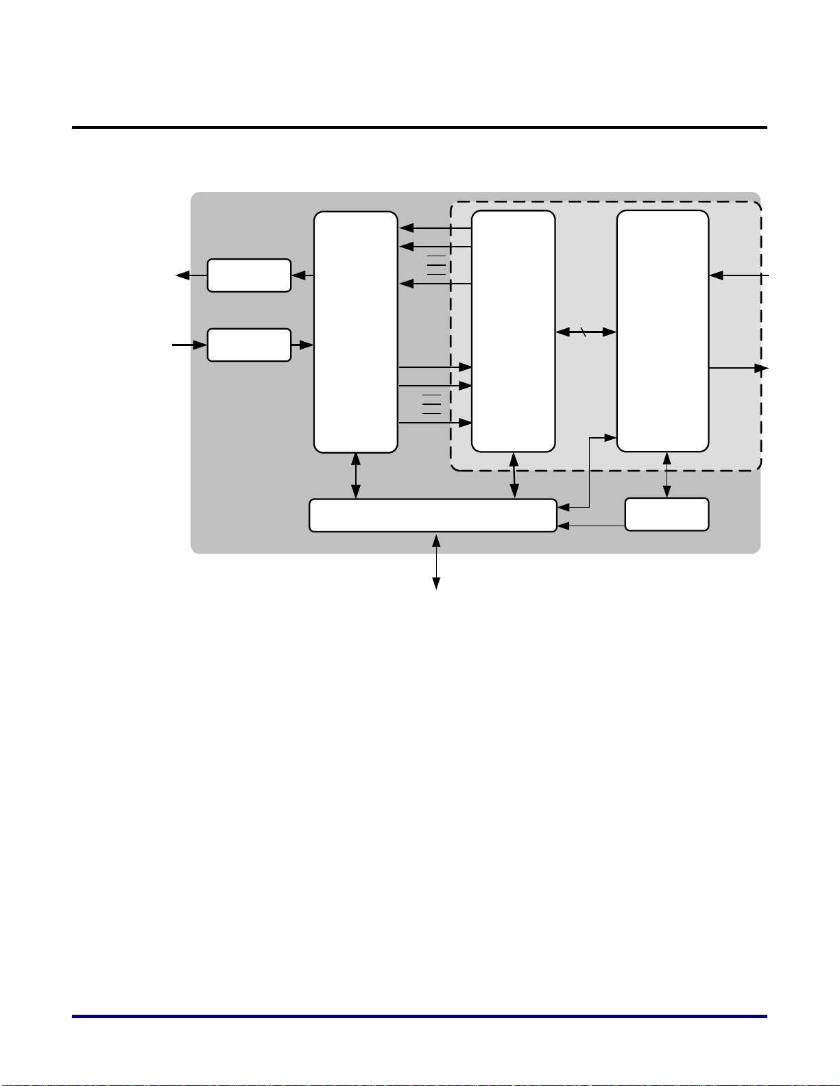
Functional Description
FPGA Fabric
Interface
10/40/100
Gigabit Ethernet
Hard IP Core
sbus
12 RX
SerDes
Lanes
12 TX
SerDes
Lanes
Media
Access
Controller
(MAC)
Physical
Coding
Sublayer
(PCS)
RX FIFO
TX FIFO
Configuration / Control / Statistics
Physical
Media
Attachment
(PMA)
JTAG
Physical
Interface
(PHY)
10 UG029, September 6, 2013
Figure 1: 10/40/100 Gigabit Ethernet MAC Block Diagram
On the FPGA Fabric interface side, the 10/40/100 Gigabit Ethernet MAC and PCS Core
implements a flexible FIFO interface that can be connected to a custom user application.
On the Ethernet line side, the Core implements a 12 x 20-Bit line interface to the Physical
Media Attachment (PMA) module which consists of 12 x 10G SerDes lanes directly connected
to the FPGA I/O pins. The 12 SerDes lanes in the PMA module can be utilized independently
of the 10/40/100G Ethernet MAC. The physical interface for this module in configured via the
10/40/100G Ethernet MAC IP configuration wizard. Details of the Achronix SerDes I/O are
beyond the scope of the user guide. A separate user guide is available for the SerDes I/O
functionality.
X/XL/CGMII Loopbacks
Each PCS Layer implements a X/XL/CGMII side loopback to the MAC, which returns all data
from the MAC transmit back to the MAC receive side without passing through any of the
PCS blocks.
When the loopback is enabled the transmitted data is treated depending on the mode of
operation as follows:
10G Base-R: The PCS transmits the constant pattern of 0x00ff (8x'1' bits alternating
with 8x'0' bits) to the SerDes line interface.
40G/100G Base-R: The PCS transmits the MAC transmit data unchanged to the SerDes
line interface (as defined by IEEE802.3ba).
Page 11

11
UG029, September 6, 2013
Page 12
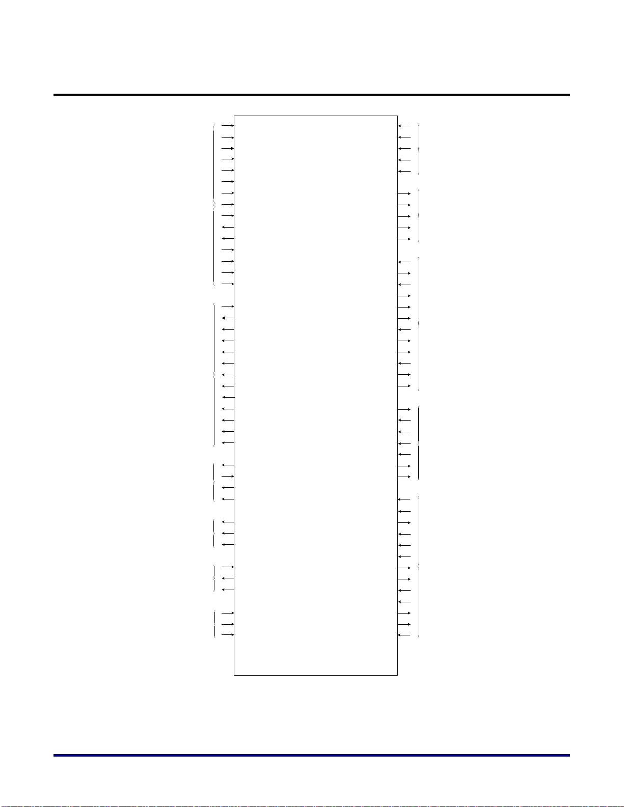
Interface Signal List
ref_clk
reset_ff_rx_clk_n[2:0]
reset_ff_tx_clk_n[2:0]
reset_n
reset_ref_clk_n
align_done[2:0]
block_lock[11:0]
hi_ber[11:0]
loc_fault[11:0]
rem_fault[11:0]
pma_{11:0}_pd[1:0]
pma_rx_cdr_lck2dat[11:0]
pma_rx_iddq_n[11:0]
pma_rxready[11:0]
pma_rxstat[11:0]
pma_sig_detect[11:0]
pma_synth_iddq_n[11:0]
pma_synthready[11:0]
pma_synthestat[11:0]
pma_tx_iddq_n[11:0]
pma_txready[11:0]
pma_txstat[11:0]
serdes_aprobe[11:0]
serdes_ck_ref_m[11:0]
serdes_ck_ref_p[11:0]
serdes_rx_m[11:0]
serdes_rx_p[11:0]
serdes_tx_m[11:0]
serdes_tx_p[11:0]
i_sbus_sw_rst
sbus_clk
reg_ts_avail[11:0]
reset_sbus_clk_n
i_sbus_req
i_sbus_data[1:0]
o_sbus_data[1:0]
o_sbus_ack
pma_{11:0}_i_sbus_req
pma_{11:0}_i_sbus_data[1:0]
pma_{11:0}_o_sbus_data[1:0]
pma_{11:0}_o_sbus_ack
pma{11:0}_pd
Fabric Transmit FIFO Interface
Fabric Receive FIFO Interface
Priority Flow Control
Transmitted Frame Status
Auto-Negotiation Control & Status
Global Signals
MAC/PCS Status
PMA TX/RX Interface
FPGA SerDes Off-Chip I/O pins
MAC & PMA Serial Control Bus
Time Stamp Timer
sys_clk
ff_clk[2:0]
ff_tx_data[767:0]
ff_tx_wren[11:0]
ff_tx_sop[11:0]
ff_tx_eop[11:0]
ff_tx_mod[71:0]
ff_tx_err[11:0]
ff_tx_crc[11:0]
ff_tx_rdy[11:0]
ff_tx_ovr[11:0]
ff_tx_id[3:0]
ff_tx_ts_frm
ff_tx_preamble_val
ff_tx_preamble[55:0]
ff_rx_rdy[11:0]
ff_rx_data[767:0]
ff_rx_dval[11:0]
ff_rx_sop[11:0]
ff_rx_eop[11:0]
ff_rx_mod[71:0]
ff_rx_err[11:0]
ff_rx_vlan[23:0]
ff_rx_afull[11:0]
ff_rx_err_stat[23:0]
ff_rx_ts[31:0]
ff_rx_preamble_val
ff_rx_preamble[55:0]
pfc_mode[11:0]
ff_tx_pfc_xoff{11:0}[7:0]
ff_tx_pfc_ack[11:0]
ff_rx_pfc_xoff{11:0}[7:0]
tx_ts_val
tx_ts_id[3:0]
tx_ts[31:0]
an_ena[11:0]
an_int[11:0]
an_done[11:0]
frc_in[31:0]
ts_clk
reset_ts_clk_n
12 UG029, September 6, 2013
Figure 2: Interface Signal List
Page 13

13
Interface Signal Descriptions
Signal Name
Mode
Description
ref_clk
In
Reference Clock. Must be at least 652 MHz +/- 100ppm.
reset_n
In
Active low hard reset for all SerDes channels.
reset_ref_clk_n
In
Active low reset signal for ref_clk clock domain.
reset_ts_clk_n
In
Active low reset signal for ts_clk clock domain (if ts_clk is
used, see below).
reset_ff_tx_clk_n[2:0]
In
Active low reset signal for ff_tx_clk[2:0] clock domains.
reset_ff_rx_clk_n[2:0]
In
Active low reset signal for ff_rx_clk[2:0] clock domains.
Signal Name
Mode
Description
sys_clk
In
FPGA fabric System Clock. All the FIFO signals are
synchronized on sys_clk rising edge. The minimum
frequency for the system clock is a function of the interface
rate:
10G: at least 155 MHz
40G: at least 177 MHz
100G: at least 295 MHz
ff_clk[2:0]
In
FIFO Reference Clocks per FIFO group. Can be set to any
value required to get the required bandwidth on the FIFO
768-Bit interface. Can be independent from the System
clock, however the FIFO clock has to be at least 357.15 MHz
to allow for the start of frame to be always aligned on lane 0
for 40G mode and may be relaxed to at least 320.51 MHz for
the 10G or 100G modes.
ff_rx_data
[767:0]
Out
Receive Data. Refer to the ‘Fabic FIFO Interface’ for the
details of how to map this 768-bit bus to the individual
10/40/100G channels.
ff_rx_dval[11:0]
Out
Receive Data Valid per segment. Asserted (set to 1) by the
MAC to indicate that data on ff_rx_data, ff_rx_sop,
ff_rx_eop, ff_rx_mod, ff_rx_err, ff_rx_vlan,
ff_rx_err_stat and ff_rx_ts is valid.
ff_rx_sop[11:0]
Out
Receive Start of Frame per segment. Set to 1 when the first
data word of a frame is driven on ff_rx_data.
ff_rx_eop[11:0]
Out
Receive End of Frame per segment. Set to 1 when the final data
word of a frame is driven on ff_rx_data.
ff_rx_mod
[(12*6)-1:0]
Out
Receive Word Modulo per segment. Indicates which portion of the
final frame word is valid:
Bit 543210
000000 : ff_rx_data[63:0]/[255:0]/[511:0] is valid (for
10/40/100G)
000001 : ff_rx_data[7:0] is valid
000010 : ff_rx_data[15:0] is valid
000011 : ff_rx_data[23:0] is valid
000100 : ff_rx_data[31:0] is valid
000101: ff_rx_data[39:0] is valid
Global Signals
Receive FIFO Interface
Table 2 – Receive FIFO Interface (All syncrounous to sys_clk at user interface)
Table 1 – Global Signals
UG029, September 6, 2013
Page 14

000110: ff_rx_data[47:0] is valid
000111: ff_rx_data[55:0] is valid
001000: ff_rx_data[63:0] is valid (40/100G only)
001001: ff_rx_data[71:0] is valid (40/100G only)
.....
.....
011110: ff_rx_data[239:0] is valid (40/100G only)
011111: ff_rx_data[247:0] is valid (40/100G only)
100000: ff_rx_data[255:0] is valid (100G only)
100001: ff_rx_data[263:0] is valid (100G only)
.....
.....
111110: ff_rx_data[495:0] is valid (100G only)
111111: ff_rx_data[503:0] is valid (100G only)
ff_rx_err[11:0]
Out
Receive Frame Error per segment. Asserted with the frame's final
data word to indicate that an error was detected when receiving the
frame. The type of error is coded on the status word
ff_rx_err_stat[23:0].
ff_rx_rdy[11:0]
In
Receive Ready per segment. The ff_rx_rdy signal is asserted high
to indicate to the Receive FIFO that it may transmit ff_rx_data.
Deasserting the ff_rx_rdy signal allows the user to pause the
reception of ff_rx_data, but the Receive FIFO Almost Full flag,
ff_rx_afull, must be monitored to prevent the Receive FIFO from
overflowing, resulting is a loss of data.
ff_rx_afull[11:0]
Out
Receive FIFO Almost Full flag per segment. The ff_rx_afull flag is
asserted high when there are 15 or fewer empty locations
remaining in the Receive FIFO.
ff_rx_vlan
[(12*2)-1:0]
Out
Receive Frame VLAN Indication per segment. Asserted with the
frame’s final data word to indicate that the current frame
implements a VLAN Tag (bit 0 asserted) or a Stacked VLAN Tag
(bit 1 asserted).
ff_rx_err_stat[23:0]
Out
Receive Frame Status and Error Indications. A status word is
available for each received frame with the final word (ff_rx_eop =
1). The receive frame status ff_rx_err_stat[23:0] can be
mapped to any segment of FIFO group 0 (10G: SEG0-3, 40G:
SEG0, 100G: SEG0).
_stat[0]: Set to 1 when the current frame has an invalid length,
i.e. less than 64 octets or more than the maximum value defined in
register FRM_LENGTH, or a mismatch between the payload
received and the payload length given within the frame was
detected.
_stat[1]: Set to 1 to indicate that the current frame was received
with a CRC-32 error.
_stat[2]: Set to 1 to indicate that the current frame was received
with a wrong or unexpected code during frame reception reported
by the reconciliation sub-layer function.
_stat[3]: Set to 1 to indicate that the current frame was truncated
because of a FIFO exception (Overflow).
_stat[4]: Set to 1 to indicate that a Sequence Error (Local or
Remote) was received from the PHY device during frame reception.
_stat[5]: Set to 1 to indicate that the current Frame implements a
Stacked VLAN Tag.
_stat[6]: Set to 1 to indicate that the current frame was received
with an Error control character on the XL/CGMII interface.
_stat[7]: Set to 1 to indicate that the current Frame implements a
VLAN Tag.
_stat[23:8]: Payload length of the frame. This is a copy of the
length/type field as it is found within the frame. For VLAN frames it
is a copy of the length/type field following the 4-octet VLAN tag.
ff_rx_ts[31:0]
Out
Receive Timestamp Value. Time when the MAC detected the
14 UG029, September 6, 2013
Page 15

15
SFD of the frame.
Valid with ff_rx_sop. The receive timestamp
ff_rx_ts[31:0] can be mapped to any segment of FIFO
group 0 (10G: SEG0-3, 40G: SEG0, 100G: SEG0).
ff_rx_preamble_val
Out
Receive Frame Preamble Valid Indication. Asserted (set to
1) to indicate that a valid preamble is available on pin
ff_rx_preamble[55:0].
Note: Since the signal ff_rx_preamble_val is not a
pulse, the application should sample
ff_rx_preamble[55:0] when ff_rx_sop is set to 1.
ff_rx_preamble[55:0]
Out
Receive Frame Preamble. 56-Bit preamble of the current
frame, valid when ff_rx_preamble_val is set to 1. The
receive frame preamble ff_rx_preamble[55:0] can be
mapped to any segment of FIFO group 0 (10G: SEG0-3,
40G: SEG0, 100G: SEG0).
Signal Name
Mode
Description
ff_tx_data
[767:0]
In
Transmit Data. Refer to the ‘Fabic FIFO Interface’ for the
details of how to map this 768-bit bus to the individual
10/40/100G channels.
ff_tx_wren[11:0]
In
Transmit Data Write Enable per segment. Asserted by the
Transmit application to write data into the MAC Core FIFO.
ff_tx_sop[11:0]
In
Transmit Start of Frame per segment. Set to 1 when the
first data word of a frame is driven on ff_tx_data.
ff_tx_eop[11:0]
In
Transmit End of Frame per segment. Set to 1 when the
final data word of a frame is driven on ff_tx_data.
ff_tx_mod
[(12*6)-1:0]
In
Transmit Word Modulo per segment. Indicates which
portion of the final frame word is valid:
Bit 543210
000000 : ff_tx_data[63:0]/[255:0]/[511:0] is
valid (for 10/40/100G)
000001 : ff_tx_data[7:0] is valid
000010 : ff_tx_data[15:0] is valid
000011 : ff_tx_data[23:0] is valid
000100 : ff_tx_data[31:0] is valid
000101 : ff_tx_data[39:0] is valid
000110 : ff_tx_data[47:0] is valid
000111 : ff_tx_data[55:0] is valid
001000 : ff_tx_data[63:0] is valid (40/100G only)
001001: ff_tx_data[71:0] is valid (40/100G only)
.....
.....
011110: ff_tx_data[239:0] is valid (40/100G only)
011111: ff_tx_data[247:0] is valid (40/100G only)
100000: ff_tx_data[255:0] is valid (100G only)
100001: ff_tx_data[263:0] is valid (100G only)
.....
.....
111110: ff_tx_data[495:0] is valid (100G only)
Transmit FIFO Interface
Table 3 – Transmit FIFO Interface (all synchronous to ff_tx_clk[2:0])
UG029, September 6, 2013
Page 16

111111: ff_tx_data[503:0] is valid (100G only)
ff_tx_err[11:0]
In
Transmit Frame Error per segment. Asserted with the
frame’s final data word to indicate that the transmitted
frame is invalid. When ff_tx_err is asserted, the frame
is transmitted to the XL/CGMII interface with a transmit
error.
ff_tx_crc[11:0]
In
Transmit CRC Append per segment. If set, a CRC field will
be appended to the frame. If cleared, the MAC does not
append a FCS to the frame. This signal must be valid
during ff_tx_sop assertion.
ff_tx_rdy[11:0]
Out
Transmit FIFO Ready per segment. When the ff_tx_rdy
signal is high, the user may send ff_tx_data to the transmit
FIFO of the addressed segment. When the ff_tx_rdy signal
is low, the transmit interface FIFO is almost full and the
user must stop sending data to the ff_tx_data port.
ff_tx_ovr[11:0]
Out
Transmit Overflow Error per segment. Asserted (set to 1)
as long as an overflow condition persists on the application
FIFO per segment. This signal can be used to trigger an
application interrupt.
ff_tx_id[3:0]
In
Frame Identifier. An arbitrary value that must be valid
during ff_tx_eop assertion that can be used to mark
specific frames. The frame identifier ff_tx_id[3:0] can
be mapped to any segment of FIFO group 0 (10G: SEG0-3,
40G: SEG0, 100G: SEG0).
The value is available at the transmit status pins
tx_ts_id[3:0] when the frame has been transmitted to
the PHY.
Has no further meaning inside the MAC besides the
forwarding to the transmit status.
ff_tx_ts_frm
In
IEEE 1588 Timing Frame Indication that must be valid
during ff_tx_eop assertion. The frame indication
ff_tx_ts_frm can be mapped to any segment of FIFO
group 0 (10G: SEG0-3, 40G: SEG0, 100G: SEG0). Allows
the application to mark specific 1588 event frames. When
set for a frame, its transmit timestamp will be returned on
tx_ts[31:0]
ff_tx_preamble_val
In
Transmit Frame Preamble Valid Indication. Should be
asserted with ff_tx_sop to indicate that the current frame
should be sent with the preamble provided on
ff_tx_preamble[55:0].
ff_tx_preamble[55:0]
In
Transmit Frame Preamble. 56-Bit preamble inserted in the
current frame, must be valid when ff_tx_preamble_val
is set to 1. The transmit frame preamble
ff_tx_preamble[55:0] can be mapped to any segment
of FIFO group 0 (10G: SEG0-3, 40G: SEG0, 100G: SEG0).
Signal Name
Mode
Description
pma_{11:0}_pd{1:0]
Input
Individual Lane power down state control:
11 – Coma Power State (P2) - Everything but receiver
detection + signal detect is disabled. Minimum power
consumption
PMA TX/RX Interface
16 UG029, September 6, 2013
Table 4 – PMA TX/RX Interface
Page 17

17
10 – Slumber Power State (P1) - PLL is enabled. CDR
and Driver are disabled. Increased power consumption
01 – Doze Power State (P0s) - Everything but transmit
driver is enabled. Apprx. 20-30mW saved from the Wake
state.
00 – Wake Power State (P0) - Everything is Asserted.
Maximum power consumption.
pma_rx_cdr_lck2dat
[11:0]
Output
CDR Lock to Data status indicator
0 – CDR is locked to reference clock
1 – CDR is locked to data
pma_rx_iddq_n[11:0
]
Input
Individual Receive Lane disable/power-down control 1 –
Non-PD State - all analog circuits are enabled 0 – PD
State - all analog circuits are disabled. Analog Receiver
impedance is placed into High Impedance mode.
pma_rxready[11;0]
Output
Receive Lane Ready Status Signal:
0 – RX Lane is not ready for data transmission
1 – RX Lane is ready for data transmission
pma_rxstat[11:0]
Output
Receive Lane State Transition Status. Indicates when the
PMA has completed a requested state transition:
0 – RX Lane has not completed its state change
1 – RX Lane has completed its state change
pma_sig_detect[11:
0]
Output
Receiver Data Detection Status Signal.
0 – Indicates no/invalid data on receive pins
1 – Indicates valid data on receive pins
pma_synth_iddq_n[
11:0]
Input
Individual Synthesizer disable/power-down control
1 – Non-PD State - all analog circuits are enabled
0 – PD State - all analog circuits are disabled
pma_synthready[11:
0]
Output
SYNTH Ready Status Signal:
0 – SYNTH is not ready for data transmission
1 – SYNTH is ready for data transmission
pma_synthstat[11:0]
Output
SYNTH state transition status. Indicates when the PMA
has completed a requested state transition:
0 – SYNTH has not completed its state change
1 – SYNTH has completed its state change
pma_tx_iddq_n[11:0
]
Input
Individual Transmit Lane disable/power-down control:
1 – Non-PD State - all analog circuits are enabled
0 – PD State - all analog circuits are disabled
Signal Name
Mode
Description
pfc_mode[11:0]
Out
Per segment Priority Flow Control Mode. For each of the
12 segments, this signal represents the setting of the
PFC_MODE configuration register bit.
See COMMAND_CONFIG Register Bit Definitions on
page 67 for more details.
ff_tx_pfc_xoff{11:0}[
7:0]
In
Per segment transmit flow control generate. When PFC
Pause mode is enabled, for each of the 12 segments, an
8-bit input vector is used to signal the creation of PFC
control frames.
When Link Pause mode is enabled, Bit 0 of each segment
is used only.
Priority Flow Control Interface
UG029, September 6, 2013
Table 5 – Priority Flow Control Interface
Page 18

ff_tx_pfc_ack[11:0]
Out
Per segment Transmit Flow Control Acknowledge. Each
segment provides an ACK back to the application when it
samples the ff_tx_pfc_xoff inputs to indicate that a
PFC/Pause control frame is about to be sent according to
the provided status.
ff_rx_pfc_xoff
[11:0][ 7:0]
Out
12 – 8bit bus interfaces on a per segment Receive Flow
Control Status. For each of the 12 segments, an 8-bit
vector indicating the current pause status for the 8
priorities based on the internal pause quanta counters that
were set when a PFC control frame was received. When
asserted, it indicates that a PFC pause condition is in
place for that priority and the upstream core logic should
not schedule further traffic for this class. When zero, this
indicates the pause condition is no longer present and
traffic can be scheduled for this class.
In Link Pause Frame mode, Bit 0 is asserted (set to 1) to
indicate that the transmit path is paused as a result of a
received XOFF Pause frame. The signal deasserts, when
the pause timer has expired and the transmitter is allowed
to transmit frames again.
Signal Name
Mode
Description
an_ena[11:0]
In
Per segment Default Auto-Negotiation Enable. If ‘1’, the autonegotiation process will start after reset de-assertion for the
respective segment. The application can also start the autonegotiation process by writing the
KXAN_CONTROL.an_enable bit with ‘1’.
an_int[11:0]
Out
Per segment Auto-Negotiation Page Received Interrupt.
Asserted when a new page is received. Active only when the
Page Received Interrupt pin is enabled by writing the
KXAN_CONTROL.page_rcv_int_en bit with ‘1’.
See
Control Register Bits (KXAN_CONTROL) page 89 for details.
an_done[11:0]
Out
Per segment Auto-Negotiation Done. If ‘1’, the autonegotiation process has completed.
Signal Name
Mode
Description
sbus_clk
In
Register Access Clock.
reset_sbus_clk_n
In
Active low reset signal for the Ethernet MAC register
interface controlled by the sbus_clk clock domain.
i_sbus_data[1:0]
In
Carries read/write indication, address and data to write
i_sbus_req
In
Asserted for 9-cycles in case of read and for 11-cycles in
case of write
i_sbus_sw_rst
In
Active high reset signal for the Serial Bus Interface
controlled by the sbus_clk clock domain.
o_sbus_ack
Out
Acknowledgment from register i/f once read or write is
Auto-Negotiation Control and Status
Table 6 – Auto-Negotiation Control and Status (all synchronous to sbus_clk)
Serial Bus Interface
18 UG029, September 6, 2013
Table 7 – Serial bus Interface (all synchronous to sbus_clk)
Page 19

19
completed thru SBUS. During write it is valid for one cycle
to indicate the end of the transfer. This is asserted for 4cycles to validate 8-bit data at the end of read.
o_sbus_data[1:0]
Out
Contains read data for 4-cycles when o_sbus_ack is
asserted.
pma_[11:0]_i_sbus_
data[1:0]
In
Input serial data interface for PHY PMA internal registers.
pma_0_i_sbus_req
In
Request signal for starting a read or write transaction on the
serial interface for PHY PMA internal registers.
pma_0_o_sbus_ack
Out
Acknowledge signal for a complete read or write operation
on the serial interface for PHY PMA internal registers.
pma_0_o_sbus_dat
a[1:0]
Out
Output serial data interface for PHY PMA internal registers.
Signal Name
Mode
Description
serdes_ck_ref_m[11:0]
In
Management Data Clock.
serdes_ck_ref_p[11:0]
In
Management Data Input.
serdes_rx_m[11:0]
In
Management Data Output.
serdes_rx_p[11:0]
In
Management Data Output Enable (active low).
serdes_tx_m[11:0]
Out
Management Data transaction is ongoing
serdes_tx_p[11:0]
Out
Management Data transaction is ongoing
Signal Name
Mode
Description
tx_ts_val
Out
Timestamp Valid. Asserted for one ref_clk clock
cycle to indicate that tx_ts_id and tx_ts are valid.
The timestamp can be mapped to any segment of
FIFO group 0 (10G: SEG0-3, 40G: SEG0, 100G:
SEG0).
The signal is not asserted for internally generated
Pause frames.
tx_ts_id[3:0]
Out
Frame Identifier. The value that was provided by the
application at ff_tx_id[3:0] for the frame.
tx_ts[31:0]
Out
Frame Timestamp Value. Transmit timestamp value
for the frame sent with the sequence number set on
tx_ts_id.
Signal Name
Mode
Description
ts_clk
In
Clock for the timestamp timer.
Maximum frequency is 1/4 of the ref_clk to allow for
proper clock domain synchronization.
frc_in[31:0]
In
Current value of an externally provided free running
SerDes (off-chip) Interface
Table 8 – FPGA SerDes Off-Chip I/O pins (all synchronous to serdes_ck_ref_*)
Transmitted Frame Status
Table 9 – Transmitted Frame Status (all synchronous to ff_tx_clk[0])
Timestamp Timer
UG029, September 6, 2013
Table 10 – Timestamp Timer (all synchronous to ts_clk)
Page 20

counter (FRC). Used for timestamping.
The value typically expresses nanoseconds within the
current one second interval, hence ranging from 0 to
10^9-1.
reg_ts_avail[11:0]
Out
Per segment Register TS_TIMESTAMP contains new
data. The pin is the direct representation of the
STATUS.ts_avail register bit: It asserts when a new
timestamp is stored and it becomes deasserted when
writing the STATUS.ts_avail bit with ‘1’.
Signal Name
Mode
Description
loc_fault[11:0]
Out
Local fault state indication from MAC RS layer per
segment.
rem_fault[11:0]
Out
Remote fault state indication from MAC RS layer per
segment.
block_lock[11:0]
Out
Lane block lock indication (if 1). In 10G Mode and
SGMII PCS active it indicates proper sync to 10B
comma characters.
align_done[2:0]
Out
Multi-lane alignment done indication. Relevant in
40G/100G mode only. Uses bits 0,1,2 when operating
in 40G mode for segments 0,4,8 respectively. Uses
bit 0 only when operating in 100G mode.
hi_ber[11:0]
Out
High Bit Error rate indication from HIBER monitor for
each lane.
MAC/PCS Status Indications
Table 11 – MAC/PCS Status Indications (all synchronous to ref_clk)
20 UG029, September 6, 2013
Page 21
21
Implementation with ACE
Mode
10G
Channels
40G
Channels
100G
Channels
1
12 0 0 2 2 0 1 3 0 3 0 4 4 2 0 5 8 1 0
Software/Hardware Requirements
The ACE software suite has the following system requirements:
Platform:
Memory Requirements by design size:
Creating an Ethernet Instance
The ACE design suite documentation outlines how to install the software, launch it, and
setup your first project. Refer to ACE documentation to learn how to setup your first project.
Configuring the 10/40/100G Ethernet Core
o 64 bit Linux (RHEL/Centos)
o 64bit Windows 7
o Minimum: 12GB
o Recommended for < 100k LUTs: 16GB
o Recommended for 100k – 400k LUTs: 24GB
o Recommended for > 400k LUTs: 32GB
The 10/40/100G Ethernet core is automatically generated from a design wizard in the ACE
design tool suite. Simply launch the IP wizard, select the 10/40/100G Ethernet core from the
list of available IP and a configuration wizard will prompt the user for configuration options.
The options that are presented will be based on the number of lanes you chose and the speed
of each lane. Only certain combinations are available and the wizard will restrict the user to
only those 5 modes available:
Table 12 – Five modes of operation
The Speedster22i 10/40/100G Ethernet MAC IP wizard configuration menu is shown below.
The “Target Device” is selected by the user from a series of drop-down menus that will limit
the options in successive option choices. If we were to select zero 100G lanes we could select
two 40G and four 10G lanes. These options are bound by the five modes of operation defined
above.
Once the lane configuration are chosen, the user will need to define the clock speeds for the
reference clock, serial bus interface clock; and the transmit and receive clock for the lane
groups. Groups of four lanes share a common clock source.
UG029, September 6, 2013
Page 22
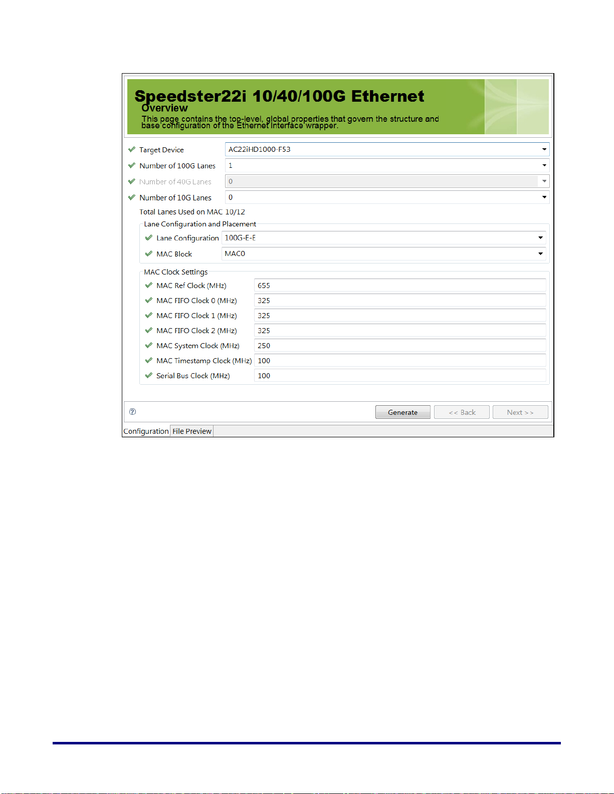
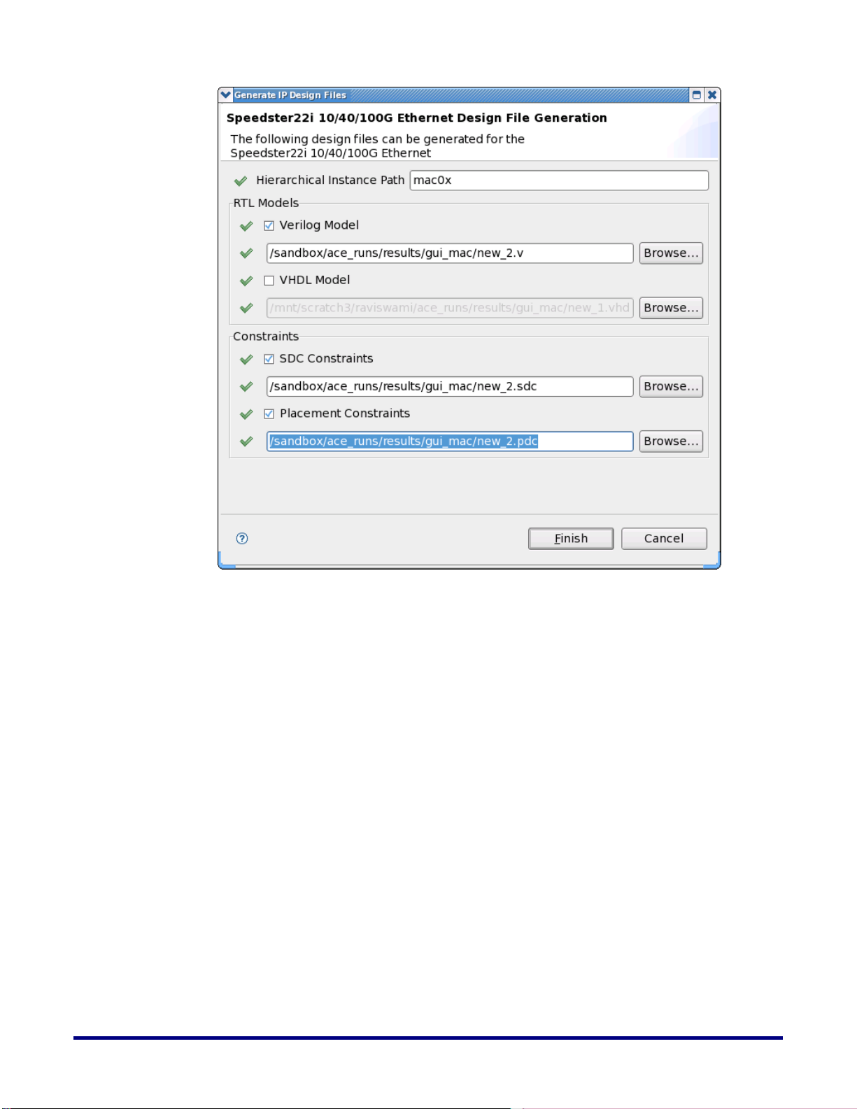
Figure 3: 10/40/100G Ethernet MAC IP Wizard
Additionally, the user will need to select the placement of the core. The MAC cores will be
located at the bottom of the device. The individual device datasheets designate the location
and number of each core.
Lastly, the user will chose the SerDes lane configuration that determines the positions of the
chosen channels. Once the IP configuration options are entered, the user can select the
“Generate” button at the bottom of the dialog box and a new screen will appear with options
regarding the type and location of the files it will generate. First the user selects the
hierarchical instance
22 UG029, September 6, 2013
Page 23
23
Figure 4: Generate IP Design Files dialog box
UG029, September 6, 2013
Page 24

FPGA Fabric Interface
The fabric interface is the primary interface for the user to connect his design to the 10/40/100
Gigabit Ethernet core. The other side of the core is the dedicated PHY SerDes interface.
The user accesses the Ethernet core via asynchronous transmit and receive FIFO’s. These
FIFO’s have programmable watermarks that are configured by the user. All transfers to/from
the user application are handled independently of the Core operation, and the Core provides
a simple interface to user applications based on a FIFO almost-full flag.
PHY Interface
The Physical Interface (PHY) side of the core is hardwired to specific external SerDes I/O
pins. These pin locations will vary with device and package options, so refer to the datasheet
for your device for these locations. The PHY interface is highly configurable with complex
interactions between configuration registers. The Achronix IP wizard will manage these
configuration options for you. However a small subset of these configuration registers will
be exposed to the user. Refer to the detailed specification on internal PHY PMA registers
later in this document. Each of the twelve PHY channels has a dedicated serial bus for
configuring registers.
Interfacing the Ethernet Core to the FPGA Fabric
Data
The data connections are labeled (ff_tx_* & ff_rx_*). In order to support any packet size, the
transmit and receive interface clocks have to run faster than the nominal required clock
frequency (100Gbps/512b = 195.31 MHz). In 100G mode of operation, worst case is 65-byte
packets, which require two 64-byte words at the user interface to the Ethernet block.
Therefore, for 100G mode, the minimum required transmit/receive interface clock rate is 295
MHz. In the 10G and 40G modes that have narrower interfaces per lane, the data packs more
efficiently, so the required transmit/receive clock rates are lower at 155 MHz. and 177 MHz.
each. There is a simple flow control interface to user application based on a FIFO flag
scheme.
Serial Bus Interface
All internal registers for in the Ethernet core are configurable though a series of 13 serial bus
interfaces. There is one for each for the 12 SERDES channels and one for the MAC/PCS core
itself.
Simulation
In addition to synthesis and place and route functions, the Achronix software flow also
supports various stages of simulation.
24 UG029, September 6, 2013
Page 25

25
.vp or .ve file extenstion
.vma file extenstion
Figure 5: Simulation Flow
Software simulation can be done pre-tool chain at the functional RTL level, post-synthesis at
the gate level, and post-route at the Achronix technology specific level.
Throughout the flow, various checkpoints can be done to insure that the design functionality
is kept intact. Figure 5 shows what files are generated at each step and how they are used in
the simulation framework.
At the RTL Design Description level, the FPGA designer’s behavioral RTL description is
compiled by the simulator.
At the Mapped Netlist level, the output of the synthesis tools (Synplify Pro
TM)
) is used. This
is the synchronous gate-level constructs that Achronix Speedster22i understands. It is a
Verilog netlist file that has have a *.vma extension.
At the Post P&R Netlist level, the output of the Achronix CAD Environment (ACE) will
generate a *_routed.vp or *_routed.ve netlist for simulation. This will exist in the project and
active implementation directory under “output”. This file is encrypted using the IEEE STD
1364-2005 Verilog encryption standard, but this file can be decrypted correctly by supported
simulators.
UG029, September 6, 2013
Page 26

Clock Distribution
The clock frequency of the SerDes interface depends on the selected SerDes datapath width
(synthesis option). The ACE GUI allows the user to pick one of several frequencies.
The Figure below shows the system clock distribution for the 10/40/100 Gigabit Ethernet
MAC and PCS Core for the 20-Bit SerDes interface.
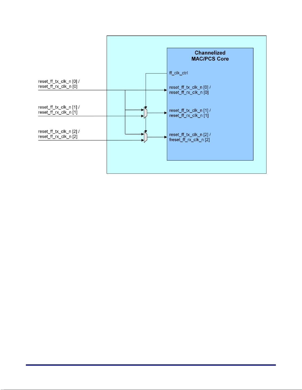
Figure 6: System clock distribution for the 20-Bit SerDes interface
On the FIFO interface, 3 individual clock signals are provided for both transmit
(ff_tx_clk[2:0]) and receive (ff_rx_clk[2:0]). When 100G mode of operation is selected, the
clock signals ff_tx_clk[2:0] and ff_rx_clk[2:0] and their respective reset lines have to be driven
from the same clock and reset sources. The system clock distribution diagram below shows
an example implementation for the external clock and reset multiplexers.
26 UG029, September 6, 2013
Page 27
27
Figure 7: Example implementation for the FIFO clock and reset multiplexers
UG029, September 6, 2013
Page 28

Reset Considerations
MAC Soft Reset
When the MAC control register (COMMAND_CONFIG) reset bit is written, the following
functions are executed:
Ongoing receive is terminated when next possible (graceful stop). A currently
received frame may be written truncated to the FIFO.
Transmit is disabled when next possible (graceful stop). This may lead to outgoing
frame corruption (frame not terminated but transmit switches to idle
immediately).
Transmit and Receive are disabled (COMMAND_CONFIG bits 0,1 reset to 0)
Pause timers are all reset and pause conditions are cleared
Receive Credit value is cleared (set 0)
RX and TX FIFOs are reset
Reset bit clears itself
FIFO / Credit Counter Reset
The receive FIFO credit counter can be initialized by writing the credit value to the MAC
register INIT_CREDIT followed by a write to register CREDIT_TRIGGER. This will enable
the MAC to begin writing received frame data into the FIFO. As long as the
CREDIT_TRIGGER has not been written, all incoming frames will be discarded.
The credit counter can be re-initialized any time during operation. This will abort any
ongoing receive activity and flush the receive FIFO (discarding frame data if any). Once the
FIFO has been flushed normal receive resumes. An ongoing transaction on the application
interface will be terminated cleanly by producing a final word with EOP and error being
asserted to the application.
PCS Reset
When the PCS control register (CONTROL1) reset bit is written, the following functions are
executed:
Alignment is lost (for 40G and 100G PCS layers) which eventually leads to local
fault indication to the MAC on XL/CGMII
Alignment FIFOs are flushed (for 40G and 100G PCS layers)
All error counters are reset to 0
Reset bit clears itself
When the reset is issued in 40G mode, the reset causes the 4 lanes of the segment to be reset.
When the reset is issued in 100G mode, the reset causes the 10 lanes used to be reset.
28 UG029, September 6, 2013
Page 29

29
Fabric FIFO Interface
Configuration
Segment ID
Datapath Bits
Clocks
1-12 x 10G
SEG0 –
SEG11
[63:0] = SEG0
[127:64] = SEG1
[191:128] = SEG2
[255:192] = SEG3
[319:256] = SEG4
[383:320] = SEG5
[447:384] = SEG6
[511:448] = SEG7
[575:512] = SEG8
[639:576] = SEG9
[703:640] = SEG10
[767:704] = SEG11
ff_clk[0] = SEG0-3
ff_clk[1] = SEG4-7
ff_clk[2] = SEG8-11
1 x 100G,
1-2 x 10G
SEG0,
SEG10-11
[511:0] = SEG0
[703:640] = SEG10
[767:704 ] = SEG11
ff_ clk[2:0] = SEG0
ff_ clk[2] = SEG10-11
1-3 x 40G
SEG0, SEG4,
SEG8
[255:0] = SEG0
[ 511:256] = SEG4
[767:512] = SEG8
ff_ clk[0] = SEG0
ff_ clk[1] = SEG4
ff_ clk[2] = SEG8
1-4 x 10G,
1-2 x 40G
SEG0-3,
SEG4, SEG8
[63:0] = SEG0
[127:64] = SEG1
[191:128] = SEG2
[255:192] = SEG3
[511:256] = SEG4
[767:512] = SEG8
ff_ clk[0] = SEG0-3
ff_ clk[1] = SEG4
ff_ clk[2] = SEG8
1-8 x 10G,
1 x 40G
SEG0-7,
SEG8
[63:0] = SEG0
[127:64] = SEG1
[191:128] = SEG2
[255:192] = SEG3
[319:256] = SEG4
[383:320] = SEG5
[447:384] = SEG6
[511:448] = SEG7
[767:512] = SEG8
ff_ clk[0] = SEG0-3
ff_ clk[1] = SEG4-7
ff_ clk[2] = SEG8
Overview
The following table shows the segment definition and datapath bit assignments for each
configuration.
Table 13 – Modes of Operation
UG029, September 6, 2013
Page 30
Transmit FIFO Interface Block Diagram
Figure 8: Transmit FIFO Interface Block Diagram
30 UG029, September 6, 2013
Page 31

31
Receive FIFO Interface Block Diagram
Figure 9: Receive FIFO Interface Block Diagram
UG029, September 6, 2013
Page 32

Credit Handling
The following figure provides an overview of the credit based application interface.
Figure 10: Credit based application interface
Receive Direction: FIFO to Application
Internally, the receive datapath FIFO implements a credit counter which defines how many
words the FIFO is allowed to deliver to the application. The credit counter is initialized by
the application at startup, to the maximum burst acceptable by the application (see registers
INIT_CREDIT and CREDIT_TRIGGER).
Once the credit counter has been initialized, the FIFO will provide data to the application as
long as it has credits available and the ff_rx_rdy signal is asserted. The user asserts ff_rx_rdy
to signal to the receive interface that it has consumed the data presently at the ff_rx_data
output. The user should monitor the ff_rx_afull flag if it is not able to continuously read the
received data. Alternatively, if the application can guarantee it is always operating faster
than the MAC will receive data, it may choose to permanently keep the ff_rx_rdy signal high.
32 UG029, September 6, 2013
Page 33

33
Transmit Direction: Application to FIFO
511 504
503 496
…
55 48
47 40
39 32
31 24
23 16
15 8
7 0
word 0
byte 63
byte 62
byte 6
byte 5
byte 4
byte 3
byte 2
byte 1
byte 0
word 1
byte 127
byte 126
byte 70
byte 69
byte 68
byte 67
byte 66
byte 65
byte 64
...
...
...
255 248
247 240
…
55 48
47 40
39 32
31 24
23 16
15 8
7 0
word 0
byte 31
byte 30
byte 6
byte 5
byte 4
byte 3
byte 2
byte 1
byte 0
word 1
byte 63
byte 62
byte 38
byte 37
byte 36
byte 35
byte 34
byte 33
byte 32
...
...
...
31 24
23 16
15 8
7 0
31 24
23 16
15 8
7 0
word 0
byte 7
byte 6
byte 5
byte 4
byte 3
byte 2
byte 1
byte 0
word 1
byte 15
byte 14
byte 13
byte 12
byte 11
byte 10
byte 9
byte 8
...
...
...
...
...
ff_tx_mod[5:0]
ff_rx_mod[5:0]
Valid Bytes
000000
ff_tx_data[511:0]
ff_rx_data[511:0]
On transmit, it is the responsibility of the application to monitor the ff_tx_rdy signal. The
user may only transfer data to the transmit FIFO when the ff_tx_rdy signal is high. When
the transmit FIFO deasserts the ff_tx_rdy signal, the user must stop sending data within
the next 8 cycles or the transmit FIFO may overflow. The user may vary the maximum
number of writes allowed after the deassertion of the ff_tx_rdy signal by changing the
threshold value of the transmit FIFO’s ff_tx_rdy almost-full flag.
Data Structure
The data structure defined in the following tables for the FIFO interface must be respected to
ensure proper data transmission on the Ethernet line.
Table 14 – 100G FIFO Interface Data Structure
Table 15 – 40G FIFO Interface Data Structure
Table 16 – 10G FIFO Interface Data Structure
Byte 0 is sent and received first to/from the line (byte 0 is sent on lane 0).
The size of a frame on the FIFO interface may not be a modulo of 512-bit, 256-bit or 64-bit for
100G, 40G or 10G mode of operation, respectively. Together with the last word of the frame,
the valid byte(s) of data is (are) defined per segment by the interface signals
ff_tx_mod[5:0] for transmit and ff_rx_mod[5:0] for receive, respectively.
Table 17 – 100G Transmit/Receive FIFO Interface Word Modulo Definition
UG029, September 6, 2013
Page 34

000001
ff_tx_data[7:0)
ff_rx_data[7:0)
000010
ff_tx_data[15:0]
ff_rx_data[15:0]
000011
ff_tx_data[23:0]
ff_rx_data[23:0]
000100
ff_tx_data[31:0]
ff_rx_data[31:0]
…
…
111110
ff_tx_data[495:0]
ff_rx_data[495:0]
111111
ff_tx_data[503:0]
ff_rx_data]503:0]
ff_tx_mod[5:0]
ff_rx_mod[5:0]
Valid Bytes
000000
ff_tx_data[255:0], ff_rx_data[255:0]
000001
ff_tx_data[7:0], ff_rx_data[7:0]
000010
ff_tx_data[15:0], ff_rx_data[15:0]
000011
ff_tx_data[23:0], ff_rx_data[23:0]
000100
ff_tx_data[31:0], ff_rx_data[31:0]
…
…
011110
ff_tx_data[239:0], ff_rx_data[239:0]
011111
ff_tx_data[247:0], ff_rx_data[247:0]
100000 - 111111
invalid
Table 18 – 40G Transmit/Receive FIFO Interface Word Modulo Definition
Note: Only datapath bit assignment for segment 0 is shown. The bit assignments for segments 4 and
8 are defined accordingly.
34 UG029, September 6, 2013
Page 35

35
Table 19 – 10G Transmit/Receive FIFO Interface Word Modulo Definition
ff_tx_mod[5:0]
ff_rx_mod[5:0]
Valid Bytes
000000
ff_tx_data[63:0], ff_rx_data[63:0]
000001
ff_tx_data[7:0], ff_rx_data[7:0]
000010
ff_tx_data[15:0], ff_rx_data[15:0]
000011
ff_tx_data[23:0], ff_rx_data[23:0]
000100
ff_tx_data[31:0], ff_rx_data[31:0]
000101
ff_tx_data[39:0], ff_rx_data[39:0]
000110
ff_tx_data[47:0], ff_rx_data[47:0]
000111
ff_tx_data[55:0], ff_rx_data[55:0]
001000 - 111111
invalid
Note: Note: Only datapath bit assignment for segment 0 is shown. The bit assignments for segments
1 to 11 are defined accordingly.
The user application does not have to manage the Ethernet frame formats in full detail. It
needs to provide and will receive an Ethernet frame with the following structure:
Ethernet MAC Destination Address
Ethernet MAC Source Address
Optional 802.1q VLAN Tag (VLAN Type and VLAN Info fields)
Ethernet Length / Type field
Payload
Frames on the FIFO interface do not contain preamble and SFD fields, which are inserted and
discarded by the MAC on transmit and receive, respectively.
On receive, CRC can be stripped or passed through transparently. The Payload length must
not exceed the value programmed in the Core configuration register FRM_LENGTH.
On transmit, padding and CRC can be provided by the user application, or appended
automatically by the MAC independent for each frame. No size restrictions apply.
Note: On transmit, if the Core configuration register TX_ADDR_INS is set to 1, the byte 6 to 11 of
each frame can be set to any value since the MAC will overwrite the bytes with the MAC address
programmed in registers MAC_ADDR_0 and MAC_ADDR_1.
UG029, September 6, 2013
Page 36

Table 20 – FIFO Interface Frame Format
Byte Number
Field
0 to 5
Destination MAC Address
6 to 11
Source MAC Address
12 to 13
Length / Type Field
14 to N
Payload Data
Byte Number
Field
0 to 5
Destination MAC Address
6 to 11
Source MAC Address
12 to 15
VLAN Type and VLAN Info
16 to 17
Length / Type Field
18 to N
Payload Data
VLAN tagged frames are also supported on both transmit and receive and implement
additional information (VLAN Type and Info fields).
Table 21 – FIFO Interface VLAN Frame Format
Note: The standard defines that the least significant byte of the MAC address is sent/received first,
while for all other header fields (i.e. Length / Type, VLAN Tag, VLAN Info and Pause Quanta), the
most significant byte is sent/received first.
36 UG029, September 6, 2013
Page 37

37
FIFO Interface Transmit Operation
sys_clk
ff_tx_wren[0]
ff_tx_data[511:0]
ff_tx_mod[5:0]
ff_tx_sop[0]
ff_tx_eop[0]
ff_tx_err[0]
ff_tx_preamble_val
ff_tx_preamble[55:0]
The application layer drives data and controls based on the configuration mode. Note that for
improved readability, the following figures only show data transfers for segment 0 in 100G
mode of operation. For all other segments in other configuration modes, the corresponding
signals need to be defined accordingly.
The user application asserts the FIFO write enable signal (ff_tx_wren[0]) to transfer data
to the MAC Core Transmit FIFO segment 0.
The user application must send the first word of a frame with the start of frame signal
(ff_tx_sop[0]) and the last word with the end of frame signal (ff_tx_eop[0]) asserted.
With the last word, a word modulo signal (ff_tx_mod[5:0]) must indicate which portion
of the bus is valid. Also the error signal (ff_tx_err[0]) and CRC append signal
(ff_tx_crc[0]) must be valid.
In case of a FIFO overflow, the Core asserts an overflow indication signal (ff_tx_ovr[0])
as long as the overflow condition persists.
Optionally a user specific preamble can be provided on ff_tx_preamble[55:0]. To
indicate a valid preamble, ff_tx_preamble_val should be asserted together with
ff_tx_sop. Note that the user defined preamble signals can only be mapped to any
segment of FIFO group 0 (10G: SEG0-3, 40G: SEG0, 100G: SEG0). For all other segments, a
user defined preamble can be specified through the control register interface.
UG029, September 6, 2013
Figure 11: FIFO Transmit Interface – Single Frame Transfer
The user application can pause a frame transfer by de-asserting the data write enable signal
(ff_tx_wren[0]) for one or multiple clock cycles. The data transfer stops immediately
when ff_tx_wren[0] is de-asserted. The transfer immediately restarts when the user
application re-asserts ff_tx_wren[0].
Page 38

sys_clk
ff_tx_wren[0]
ff_tx_data[511:0]
ff_tx_mod[5:0]
ff_tx_sop[0]
ff_tx_eop[0]
ff_tx_err[0]
Figure 12: FIFO Transmit Interface – Frame Transfer with User Application Pause
sys_clk
ff_tx_wren[0]
ff_tx_data[511:0]
ff_tx_mod[5:0]
ff_tx_sop[0]
ff_tx_eop[0]
ff_tx_err[0]
sys_clk
ff_tx_wren[0]
ff_tx_data[511:0]
ff_tx_mod[5:0]
ff_tx_sop[0]
ff_tx_eop[0]
ff_tx_err[0]
By keeping the write enable signal (ff_tx_wren[0]) asserted between two consecutive
frames, the user application can send back-to-back frames to the MAC Core.
Figure 13: FIFO Transmit Interface – Back-to-Back Frame Transfer
An error from the user application can be reported to the MAC Core by asserting
ff_tx_err[0] at the end of a frame transfer to the FIFO [1]. The frame is then transferred to
the PCS with an Error control code during the frame transfer.
38 UG029, September 6, 2013
Figure 14: FIFO Transmit Interface – Frame Transfer with Error
Page 39

39
The transmit FIFO interface is protected against the following invalid signaling conditions:
Missing SOP: All ff_tx_wren assertions prior to ff_tx_sop assertion are ignored
Missing EOP: Assertion of ff_tx_sop within a frame (i.e. no previous EOP
occurred) is ignored. This error condition is latched and will cause the frame to be
sent with an error indication (i.e. as if the ff_tx_err signal was asserted)
FIFO Interface Receive Operation
On the receive FIFO interface, the MAC Core initiates frame transfers to the user application.
The Core provides data on the FIFO interface based on the configuration. Note that for
improved readability, the following figures only show data transfers for segment 0 in 100G
mode of operation. For all other segments in other configuration modes, the corresponding
signals are provided accordingly.
An internal credit counter is used to determine when the user application is ready to accept
data. Upon writing of the credit trigger register, the credit counter is loaded with a
programmable initial credit value. For each valid output cycle, the credit counter is debited
by 1. When the credit counter reaches 0, the MAC Core stops sending data to the output
FIFO. The credit counter is issued credits when the user reads the FIFO by asserting the
ff_rx_rdy[0] signal. The assertion of ff_rx_rdy[0] signals to the FIFO interface that
the user has consumed the ff_rx_data currently at the output of the FIFO. Upon the
assertion of ff_rx_rdy[0], the MAC Core resumes transmitting data to the user
application. Valid data is associated with a valid signal (ff_rx_dval[0]). If the user
application is fast enough to receive the output data continuously, it may tie the
ff_rx_rdy[0] signal high and consume the FIFO output data when the valid signal
ff_rx_dval[0] is high. If the user application needs to pause the output FIFO, it may
deassert ff_rx_rdy[0], while also monitoring the FIFO’s almost-full flag
ff_rx_afull[0] to prevent the output FIFO from overflowing.
The MAC Core asserts a start of frame signal (ff_rx_sop[0]) at the beginning of a frame
and an end of frame signal (ff_rx_eop[0]) with the last word of the frame. In addition, a
word modulo (ff_rx_mod[5:0]) and status information (ff_rx_err_stat[23:0]) is
provided with the last word of the frame. Note that the receive status
ff_rx_err_stat[23:0] can only be mapped to any segment of FIFO group 0 (10G: SEG03, 40G: SEG0, 100G: SEG0).
Optionally a user specific frame preamble is provided on ff_rx_preamble[55:0]. To
indicate a valid preamble, ff_rx_preamble_val is asserted together with ff_rx_sop[0].
Note that the user defined preamble signals can only be mapped to any segment of FIFO
group 0 (10G: SEG0-3, 40G: SEG0, 100G: SEG0).
UG029, September 6, 2013
Page 40

sys_clk
ff_rx_data[511:0]
ff_rx_sop[0]
ff_rx_eop[0]
ff_rx_mod[5:0]
ff_rx_err[0]
ff_rx_vlan[1:0]
ff_rx_err_stat[23:0]
ff_rx_dval[0]
ff_rx_rdy[0]
ff_rx_preamble_val
ff_rx_preamble[55:0]
sys_clk
ff_rx_data[511:0]
ff_rx_sop[0]
ff_rx_eop[0]
ff_rx_mod[5:0]
ff_rx_err[0]
ff_rx_vlan[1:0]
ff_rx_err_stat[23:0]
ff_rx_dval[0]
ff_rx_rdy[0]
ff_rx_preamble_val
ff_rx_preamble[55:0]
Figure 15: FIFO Receive Interface – Single Frame Transfer
A frame transfer is stopped when the internal credit counter reaches 0. When the user
application is able to accept data again, the credit update signal is asserted by the user
application, which increments the internal credit counter. When the credit counter is nonzero, the MAC Core restarts the data transfer.
40 UG029, September 6, 2013
Figure 16: FIFO Receive Interface – Frame Transfer with data valid signal not continuously high
Page 41

41
When an Ethernet frame is received with an error, the frame is transmitted to the user
sys_clk
ff_rx_data[511:0]
ff_rx_sop[0]
ff_rx_eop[0]
ff_rx_mod[5:0]
ff_rx_err[0]
ff_rx_vlan[1:0]
ff_rx_err_stat[23:0]
ff_rx_dval[0]
ff_rx_rdy[0]
application with the frame error signal (ff_rx_err[0]) asserted with the last word of the
frame.
In addition, the MAC Core provides a 24-Bit error status word (ff_rx_err_stat[23:0])
that gives an indication on the error source (see section "" for details). Note that the receive
status ff_rx_err_stat[23:0] can only be mapped to any segment of FIFO group 0 (10G:
SEG0-3, 40G: SEG0, 100G: SEG0).
Figure 17: FIFO Receive Interface – Frame Transfer with Error
The user may pause the output of the receive FIFO by deasserting the ff_rx_rdy[0] signal.
The ff_rx_rdy[0] indicates that the user circuit has consumed the current data word at the
output of the receive FIFO. The following figure illustrates how the user may pause the data
output from the receive FIFO.
UG029, September 6, 2013
Page 42

sys_clk
ff_rx_data[511:0]
ff_rx_sop[0]
ff_rx_eop[0]
ff_rx_mod[5:0]
ff_rx_err[0]
ff_rx_vlan[1:0]
ff_rx_err_stat[23:0]
ff_rx_dval[0]
ff_rx_rdy[0]
ff_rx_preamble_val
ff_rx_preamble[55:0]
Figure 18: FIFO Receive Interface – Frame Transfer with User Pause
Frame Status
When frame reception terminates, the MAC Core writes a status word in a dedicated internal
FIFO to report information and events to the user application per frame. The status is
available with each frame with the last word of the frame (ff_rx_eop asserted) and is
presented on the ff_rx_err_stat[23:0] data bus.
Invalid length (frame too long/short)
CRC-32 error
Link error (code violation)
FIFO overflow exception
Sequence error (e.g. local or remote fault)
Frame error character
VLAN/Stacked VLAN frame indication
Frame length/type field. This is a copy of the length/type field as it is found in the
frame. Note that for VLAN frames, the value immediately following the 4-octet
VLAN tag is copied here.
If any of the error conditions happened, in addition the ff_rx_err signal will be asserted
together with the frame's last word. Note that the receive status signals
ff_rx_err_stat[23:0] can only be mapped to any segment of FIFO group 0 (10G: SEG03, 40G: SEG0, 100G: SEG0). The per segment status signals ff_rx_err and
ff_rx_vlan[1:0] provide information about error conditions as well as VLAN/Stacked
VLAN frame indications to the user application on a per segment basis.
The frame status word is defined in the table below.
42 UG029, September 6, 2013
Page 43

43
Table 22 – Frame Status Word Bits
Bit #
Name
Description
0
LENGTH_ERROR
Set to ‘1’ if the frame has an invalid length. This can be
either a too long frame (length greater than the value
programmed in register FRM_LENGTH), or a frame which
has a different amount of payload than specified in the
frame's payload length field.
Frames below 64 octets in length are never delivered to the
FIFO interface.
1
CRC_ERROR
Set to ‘1’ if the frame was received with a CRC field that did
not match the CRC calculated by the MAC Core. The frame
is invalid.
2
PHY_ERROR
Set to ‘1’ if the frame was received with an unknown control
character. The frame is invalid.
3
FIFO_OVERFLOW
Set to ‘1’ if a FIFO overflow was detected during frame
reception. The received frame is truncated by the MAC
Core and is invalid.
4
FAULT_SEQ
Set to ‘1’ if a Sequence Error (local or remote fault) has
been received from the PHY during frame reception. The
frame is invalid.
5
STACKED_VLAN
Set to ‘1’ to indicate that the frame is a Stacked VLAN
frame. This information can be used to switch the received
frame to dedicated VLAN frames processing engines.
6
TRANSMIT_ERR
Set to ‘1’ if a transmit error control character (0xFE) has
been received from the line. The frame is invalid.
7
VLAN
Set to ‘1’ to indicate that the frame is a VLAN frame. This
information can be used to switch the received frame to
dedicated VLAN frames processing engines.
23:8
PAYLOAD_LEN
Frame payload length in bytes or type information. The
copied value of the frame's length/type field. For VLAN
frames the value immediately following the 4-octet VLAN
tag is copied.
FIFO Thresholds
The Core implements programmable FIFO thresholds that provide the possibility to
dynamically change the FIFO operation and fixed Almost Full and Almost Empty thresholds
for FIFO overflow / underflow protection.
FIFO Sections Behavior (Watermarks)
The FIFO logic offers to set high- and low-watermarks by setting the configuration registers
RX_FIFO_SECTIONS and TX_FIFO_SECTIONS. The sections are defined in steps of segment
data words (10G: 32-bit, 40G: 128-bit, 100G: 384-bit).
tx/rx_section (section available) defines a low-watermark that is used to assert an
internal signal when this amount of data is available in the FIFO.
tx/rx_section_e (section empty) defines a high-watermark that is used to de-assert an
internal signal when the FIFO is filled to this level and above.
UG029, September 6, 2013
Page 44

The following figure shows the relationship of the configuration values and their respective
rx/tx_section
rx/tx_section_e
dsav
septy
1
0
0
1
RX FIFO
TX FIFO
MAC
TX
RX
ff_rx_dsav
ff_tx_septy
septy
sav
FIFO nearly full
FIFO has at least
one section of data
start transmission
send PAUSE
full indication
FIFO empty
(implicit by dval)
FIFO is full
ff_tx_rdy
signals and levels above and below the levels.
Figure 19: FIFO Sections Configuration and Signals
44 UG029, September 6, 2013
Figure 20: FIFO Sections Related Signaling
The two signals RX FIFO septy and TX FIFO sav are used internally by the MAC to generate
pause frames and start transmission of frames to the line, respectively.
The other two signals (TX FIFO septy and RX FIFO dsav) are maintained for legacy reasons
only. Note: These signals are not available in this implementation.
Page 45

45
Table 23 – FIFO Sections
Configuration
Register
Behavior
RX_FIFO_SECTIONS[15:0]
Section Available: Legacy purpose only.
Not available in this implementation.
RX_FIFO_SECTIONS[31:16]
Section Empty: If this level is reached during receive of
frames, pause frames will be generated to stop the remote
side from transmitting further data.
If set to 0, no automatic pause frame generation is done.
This function can be used only when link pause mode is
enabled. It has no effect otherwise.
TX_FIFO_SECTIONS[15:0]
Section Available: If the defined amount of data is written
into the TX FIFO, transmission will start. Transmission will
also start, when a complete frame has been written, even if
this watermark is not reached (e.g. a short frame).
As the TX FIFO must not dry out during transmission (this
would lead to a corrupted frame sent), this can help to adapt
a slower user application to the MAC. Or it can give the user
application more flexibility inserting wait states during write,
without disturbing the transmission of a frame. If set to 0,
the FIFO operates in store-and-forward mode.
TX_FIFO_SECTIONS[31:16]
Section Empty: Legacy purpose only.
Not available in this implementation.
Flow Control Interface
The MAC supports two modes of flow control:
Link Pause Flow Control: This is the standard IEEE 802.3 defined pause frame to
allow pausing the remote device connected to the link (link local pause). Upon
reception (if enabled by configuration) the transmitter is paused for the time received
in the pause frame.
Priority Flow Control (PFC): The PFC mechanism refines the pause mechanism
allowing for up to 8 traffic classes which can be paused individually. In this mode the
application will get an indication on the pause state of each class. The transmitter is
not affected and it is the responsibility of the application to stop scheduling frames for
transmission to a congested traffic class.
Only one mode can be active at a time: If a frame of the other mode is received it is treated as
a regular command frame. Depending on COMMAND_CONFIG(CMD_FRM_ENA) it is then
either discarded or forwarded to the user application but has no effect within the MAC.
See the COMMAND_CONFIG register for configuration options (see section
“COMMAND_CONFIG Register Bit Definitions” on page 67).
Link Pause Flow Control Frames
UG029, September 6, 2013
The IEEE 802.3 defined pause frame has the following format:
Page 46

Table 24 – Pause Frame Format (values in hex)
1 2 3 4 5 6 7 8 9
10
11
12
13
14
55
55
55
55
55
55
55
D5
01
80
C2
00
00
01
Preamble
SFD
Multicast Destination Address
15
16
17
18
19
20
21
22
23
24
25
26
27 - 68
00
00
00
00
00
00
88
08
00
01
hi
lo
00
Source Address
Type
Opcode
Quanta
pad (42)
69
70
71
72
xx
xx
xx
xx
CRC-32
1 2 3 4 5 6 7 8 9
10
11
12
13
14
55
55
55
55
55
55
55
D5
01
80
C2
00
00
01
Preamble
SFD
Multicast Destination Address
15
16
17
18
19
20
21
22
23
24
25
26
27
28
00
00
00
00
00
00
88
08
01
01
00
00-FF
0000-FFFF
Source Address
Type
Opcode
Class Ena
Quanta 0
29
30
31
32
33
34
35
36
37
38
39
40
41
42
0000-FFFF
0000-FFFF
0000-FFFF
0000-FFFF
0000-FFFF
0000-FFFF
0000-FFFF
Quanta 1
Quanta 2
Quanta 3
Quanta 4
Quanta 5
Quanta 6
Quanta 7
43 - 68
69
70
71
72
00
xx
xx
xx
xx
Pad (26)
CRC-32
There is no Payload Length field found within a Pause Frame and a Pause Frame is always
padded with 42 bytes (0x00).
If a pause frame with a pause value greater than zero (XOFF Condition) is received, the MAC
stops transmitting data as soon as the current Frame transfer is completed. The MAC stops
transmitting data for the value defined in pause quanta. One pause quanta fraction refers to
512 bit times.
If a pause frame with a pause value of zero (XON Condition) is received, the transmitter is
allowed to send data immediately.
Priority Flow Control (PFC) Frames
The PFC frames have the following format:
Table 25 – PFC Frame Format (values in hex)
The PFC frames use the same Length/Type field as Pause frames (0x8808). The Opcode field
0x0101 specifies the PFC frame. The 8 Class Enable bits define for each of the 8 priority
classes which class is currently enabled in the PFC frame. For each enabled priority class, a
16-bit Pause Quanta value is provided following the Class Enable field.
46 UG029, September 6, 2013
Page 47

47
Transmit Pause/PFC Operation
In transmit direction, for each of the 12 segments, an 8-bit input vector
(ff_tx_pfc_xoff<n>[7:0]) is provided to signal the creation of PFC control frames (XOFF bit).
When Link Pause Frame Mode is active, only the first input ff_tx_pfc_xoff<n>[0] for segment
n is used.
After the completion of a frame, the MAC samples these inputs and determines if, depending
on the current mode, a PFC or Link Pause control frame should be immediately scheduled.
The following cases can exist:
A pause is not in progress and the XOFF bit is set, so the current timer value is 0. In this case
a new Pause/PFC frame should be sent with the programmed quanta value.
A pause is already in progress for this priority, but the XOFF bit is now cleared, a new
Pause/PFC frame with QUANTA = 0 needs to be sent.
A pause is already in progress for that priority and the XOFF bit is still set, but the quanta
timer is between its max value and the threshold value, no new pause update is needed, so
send the next application frame.
A pause is already in progress for this priority and the XOFF bit is still set, but the timer
threshold has been reached. A refresh PFC/Pause control frame should be scheduled with the
programmed quanta timer value.
A pause is not in progress and the XOFF bit is cleared, no pause is needed, so send the next
application frame.
Receive Pause/PFC Operation
PFC Mode
When a PFC control frame is received with one or more Class Enable bits set, the
corresponding internal pause quanta counters are set with the quanta values extracted from
the PFC frame and start decrementing. For each of the 12 segments, an 8-bit status vector
(ff_rx_pfc_xoff<n>[7:0]) indicating the current pause status for the 8 priorities is provided to
the application layer. When asserted, it indicates that a PFC pause condition is in place (timer
not expired) for that priority and the upstream core logic should not schedule further traffic
for this class. When zero, this indicates the pause condition is no longer present and traffic
can be scheduled for this class.
When PFC mode is disabled, a received PFC frame is treated as a regular command frame
(see COMMAND_CONFIG(CMD_FRM_ENA)) and has no effect within the MAC.
Link Pause Mode
When a Link Pause frame is received, the quanta is extracted and loaded into an internal
timer to pause the transmitter. The transmitter continues to complete any ongoing frame
transmission and then enters a pause state where it does not read any user frames from the
transmit FIFO. When the transmitter has reached its pause state, the timer starts to
decrement. When the timer reaches 0, the transmitter resumes to normal transmission of
frames.
Only bit 0 of the segment’s status is used. The bit is asserted (1) and stays asserted as long as
the transmitter is in pause state (i.e. it will not necessarily assert at the time when the pause
frame was received). When the transmitter resumes to normal operation, the status signal
becomes 0 again.
UG029, September 6, 2013
Page 48

A configuration option (see COMMAND_CONFIG(PAUSE_IGNORE)) allows ignoring
pause frames, preventing the transmitter from being paused. When ignored the timer is not
loaded and the status bit will never assert.
48 UG029, September 6, 2013
Page 49

49
Serial Bus Interface
Port
Direction
Description
reset_sbus_clk
Input
Asynchronous reset
sbus_clk
Input
Reference clock for the serial
and parallel interface –
p1_ctl_clk
i_sbus_req
Input
Request signal for starting a
read or write transaction on
SBUS.
i_sbus_data[1:0]
Input
Input serial data of SBUS
interface. The data width can be
2bits or 1bits.
o_sbus_data[1:0]
Output
Output serial data of SBUS
interface. The data width can be
2bits or 1bits.
o_sbus_ack
Output
Acknowledgement signal for
read and write operation
complete on SBUS interface.
Overview
The Serial Bus (SBUS) Slave module is a low pin count serial interface for data transfer
between the Hard IP and the FPGA Fabric. There are 13 independent SBUS interfaces. One
32-bit interface for the 10/40/100G Ethernet MAC/PCS and an additional 12 8-bit interfaces for
the 12 PHY SerDes channels. The Serial bus protocol is decoded and converted into a parallel
register interface called P1 port to provide access to registers by the fabric/embedded IP.
Any transfer on the SBUS is initiated by asserting REQ. The first bit on the input data bus
indicates whether it is a read or a write operation. Refer to the READ/WRITE Operation for
more details. Any subsequent READ or WRITE operation should be initiated only after the
current operation is completed once o_sbus_ack is asserted by the SBUS Slave interface.
Port List
The port definitions for SBUS Slave Block are defined in the table below.
UG029, September 6, 2013
Table 26 – Port definition for SBUS Module
Read Operation
For starting a read operation the i_sbus_req is asserted for 9 cycles with the first data bit of
i_sbus_data[0] being de-asserted. The read address which is 17bit long is sent next starting
with the least significant bit.
The SBUS slave decodes the read operation and responds. Then it asserts the o_sbus_ack for
16 cycles for the case of the 32-bit data bus of the Ethernet block interface and 4 cycles for the
case of a 8-bit data of the SerDes SBUS interfaces..
The figures below show the timing diagram for operation mode on each of the 32-bit and 8bit SBUS interfaces.
Page 50

A0,1'b0 A2,A1
A16,A15
sbus_clk
i_sbus_req
i_sbus_data[1:0]
o_sbus_ack
o_sbus_data[1:0]
D1,D0 D3,D2 D31,D30D29,D28
Figure 21: Read in 32-bit Data Bus Mode
A0,1'b0 A2,A1
A16,A15
D1,D0 D3,D2 D7,D6D5,D4
sbus_clk
i_sbus_req
i_sbus_data[1:0]
o_sbus_ack
o_sbus_data[1:0]
sbus_clk
i_sbus_req
i_sbus_data[1:0]
o_sbus_ack
A0,1'b1 A2,A1
A16,A15
D1,D0 D3,D2 D31,D30
A0,1'b1 A2,A1
A16,A15
D1,D0 D3,D2 D7,D6
sbus_clk
i_sbus_req
i_sbus_data[1:0]
o_sbus_ack
D5,D4
Figure 22: Read in 8-bit Data Bus Mode
Write Operation
For starting a write operation the i_sbus_req is asserted for 25 cycles for the case of a 32-bit
write to the Ethernet SBUS interface or 13 cycles for the case of an 8-bit write to a SerDes
SBUS interface, with the first data bit of i_sbus_d[0] being asserted. The write address which
is 17bit long is sent next with the least significant bit first. The 32-bit or 8-bit write data
follows next.
The SBUS slave decodes the write operation and asserts responds. It then asserts the
o_sbus_ack for 1 cycle on the SBUS interface indicating the completion of write operation.
The figures below shows the timing diagram for a write operation on the SBUS interface.
Figure 23: Write in 32-bit Data Bus Mode
50 UG029, September 6, 2013
Figure 24: Write in 8-bit Data Bus Mode
Page 51

51
PMA Management Interface
Power
State
Power State Description
Power
Down
The power-down power state disables the lane completely. All analog blocks are
placed in power down. Receiver input terminations are set to high impedance. All
digital blocks are placed in reset. All clocks are switched over to keep-alive clock
to ensure basic functionality is supported to exit this power state.
P2
The Coma State supports limited functionality: Signal detection and transmit
beaconing are supported as required by standards such as PCIe. All remaining
analog blocks are powered down; all digital blocks are in reset. All clocks are
switched over to keep-alive clock to ensure basic functionality is supported to exit
this power state.
P1
The Slumber state is used as a fast power down state, which has a quick
recovery time. The synthesizer must be powered up prior to entering the Slumber
state. In this state, the transmit driver is disabled in an ultra-low power Doze
Mode. The entire transmit path is disabled and relevant clocks are gated. The
receiver path is still completely powered down. All clocks derived from the PLL
are switched over to their respective clocks, from the keep-alive clock, in a glitch
free manner.
P0s
The Doze state is a low power state for the transmit portion of the PMA. The CDR
and the receiver are now completely powered up. The PMA can be receiving data
in this state, however it is not transmitting data in this state. As a result, the
transmit path is reset, and the output driver is disabled in an ultra-low-power Doze
Mode. All clocks are now fully active and have switched over to their respective
clocks, from the keep-alive clock, in a glitch free manner. The receiver Ready
signal OCTL_PCS_RXREADY_Lx_A is asserted in this state.
P0
The Ready state is the fully active state for the PMA. Both the transmit and
receive data paths are fully capable to transmit and receive data. All clocks are
now fully active and have switched over to their respective clocks, from the keep-
alive clock, in a glitch free manner. The transmitter Ready signal
OCTL_PCS_TXREADY_Lx_A is asserted in this state.
Power State Descriptions
The PMA supports the following 5 power States. Power state transitions are not allowed to
occur, while the following events are still under way:
Rate Change
Data Width Change
The user must ensure that any previously initiated event completes, prior to beginning a
power state change.
Table 27 – SerDes Power State Descriptions
Note: The PHY power state can also be controlled via the PMA memory register interface
UG029, September 6, 2013
Page 52

Table 28 – Overview of PMA Behavior During the Various Power States
IO Pin Signal
P0
P0s
P1
P2
Power
Down
Hard
Reset
Power State Controls and Status
IRST_PCS_POR_B_A
1’b1
IRST_PCS_HARD_TXRX_Lx_B_A
1’b1
1’b0
IPD_PCS_[TX,RX]_Lx_B
1’b1
1’b0
IPD_PCS_SYNTH_B
1’b1
1’b0
ICTL_PCS_PSTATE_Lx_[1:0]
2’b00
2’b01
2’b10
2’b11
2’b??
OCTL_PCS_[TX,RX]_READY_Lx_A
1’b1
1’b0
OCTL_PCS_[TX,RX]_STATUS_Lx_A
1’b1
1’b0
OCTL_PCS_SYNTH_READY_A
1’b1
1’b0
OCTL_PCS_SYNTH_STATUS_A
1’b1
1’b0
Transmit Lane Controls and Status
OCK_PCS_TXWORD_PMA_Lx
TX Byte Clock
Keepalive
ICK_PCS_TXWORD_Lx
TX Byte Clock
Keepalive
IDAT_PCS_TXWORD_Lx_[X:0]
Active
5’h00000
ICTL_PCS_TXDETECTRXREQ_Lx_A
1’b0
Depends on Interface
1’b0
OCTL_PCS_TXDETECTRXSTAT_Lx_A
1’b0
Depends on Receiver
Detection Results
1’b0
ICTL_PCS_TXBEACON_Lx_A
1’b0
Depends on
Interface
1’b0
Receive Lane Controls and Status
OCK_PCS_RXWORD_Lx
RX Byte Clock
Keepalive
ODAT_PCS_RX[A,B]WORD_Lx_[X:0]
Recovered Data
5’h00000
OCTL_PCS_RXSIGNALDETEC_Lx_A
Depends on Far End
1’b0
OCTL_PCS_RXCDRLOCK2DATA_Lx_A
Depends on Far End
1’b0
Output Clocks
OCK_PCS_POSTDIV
Postdiv Clock
Keepalive
OCK_PCS_REF
Reference Clock
Keepalive
52 UG029, September 6, 2013
Page 53

53
Power State Sequencing
The following diagram demonstrates the allowed power state transitions for the PMA:
Figure 25: Power State Transitioning Diagram
UG029, September 6, 2013
Page 54

Auto-Negotiation
Overview
Each PCS layer implements an auto-negotiation function that allows the local device to
advertise supported modes of operation to another device at the remote end of an Ethernet
link, and to detect corresponding operational modes the remote device may be advertising. It
is used in backplane applications (Base-KR).
The auto-negotiation function in the PCS layers does not implement Parallel Detection in
hardware due to the ambiguity of the PCS interface for 10G, 40G and 100G modes of
operation. It is therefore the responsibility of the application layer to perform Parallel
Detection when the remote device does not support auto-negotiation or when autonegotiation is disabled.
The page exchange between link partners is done through the auto-negotiation function registers
function registers (KXAN_CONTROL, KXAN_STATUS, KXAN_ABILITY_0/1/2,
KXAN_REM_ABILITY_0/1/2, AN_XNP_0/1/2, LP_AN_XNP_0/1/2, BP_ETH_STATUS,
BP_ETH_STATUS,
see
54 UG029, September 6, 2013
Page 55

55
Control Register Bits (KXAN_CONTROL) through Next page Ability Register Bits (AN_XNP
Step#
Function
Related
Registers
Description
1
Initialize:
- Program
Ability Registers
- Clear Status
latches
KXAN_ABILITY0..2
KXAN_STATUS
Defines the base page abilities that are
exchanged first during autonegotiation.
Needs to be set according to the wanted
features before autonegotiation can be
enabled.
The status register should be read prior
to enabling autonegotiation to reset all
latches that may be active from a
previous use of the autonegotiation.
2
Enable
Autonegotiation
KXAN_CONTROL
Enable autonegotiation (bit12).
Here also the NextPage control (bit13)
must be set if next page exchanges are
wanted (i.e. local device needs to
transmit next page messages and has
set bit15 in AN_ABILITY0). Only after this
Start
Initialize
Autonegotiation
Done
Enable
Autonegotiation
Exchange
Next Page
Next
Page?
Yes
No/Done
Configure
PCS Layers
Reset
PCS Layers
AN_STATUS(page received)
Wait Base Page
Exchange
Wait Autoneg
completed
an_done +
AN_STATUS
AN_STATUS(page received)
Note: now the statemachine
enters AN_GOOD_CHECK
and updates
BP_ETH_STATUS
/ LP_AN_XNP) for details).
Usage
After reset, auto-negotiation is disabled. To use it, the following steps would be typically
needed (as a suggestion) for a channel.
UG029, September 6, 2013
Figure 26: Auto negotiation Use Flow
Table 29 – Auto-Negotiation Usage
Page 56

control bit has been set the AN_XNP
registers become writeable.
When NextPage control is disabled
(bit13=0), a so-called null-next-page is
automatically set and will be returned to
the remote device for any next page
exchanges requested by the remote.
3
Wait for base
page exchange
completion
KXAN_STATUS
When the Page Received (bit6) is set the
base page exchange has completed.
The remote device's abilities are then
available in the KXAN_REM_ABILITY
registers.
Note: If the remote device is not capable
of autonegotiation the flow will be stuck in
this state. A timeout should be
implemented to exit autonegotiation if no
reaction is found.
4
(opt)
Perform next
page
exchanges
AN_XNP_0..2
KXAN_STATUS
If required to exchange next page
messages, this can be performed after
the base page exchange has completed.
Otherwise this step is skipped.
A write to the AN_XNP2 register forwards
the information to the autonegotiation
statemachine (i.e. sets
mr_next_page_loaded flag), hence must
be written after AN_XNP0,1.
The Page Received (bit6) status register
bit will now indicate whenever a next
page message has been exchanged and
the next page message's Toggle and Ack
bits are used to perform next page
handshaking (AN_XNP/LP_AN_XNP).
5
Configure PCS
Layers
BP_ETH_STATUS
ACT_CTL_SEG
MODE_CTL_SEG
Now the PCS layers need to be enabled
as indicated by the the remote device's
ability received (KXAN_REM_ABILITY)
and resolved as indicated in
BP_ETH_STATUS.
Note: if the remote device continues to
send next-page messages (even if the
local devices has no or no more next
pages to send), the BP_ETH_STATUS
will not be updated until all next-page
exchanges are completed (i.e. not before
statemachine enters AN_GOOD_CHECK
state). The BP_ETH_STATUS has none
of the technology bits set as long as page
exchanges are ongoing.
See 0, Core Configuration Registers for
details on configuring the modes.
6
Reset PCS
Layers
PCS_CONTROL
If the PCS layer configurations are
changed a soft-reset should be
performed after enabling it.
7
Wait for
autonegotiation
completion
KXAN_STATUS
Once the correct PCS layers (and
optional link training) are configured, the
Autonegotiation function will wait for a
proper link and indicate completion when
the link is up.
56 UG029, September 6, 2013
Page 57

57
As soon as the PCS has established the
link (block_lock asserted and
align_done set accordingly for 40G
and 100G mode of operation), the autonegotiation process completes and
asserts the signal an_done.
Note that autonegotiation cannot
complete until the PCS layer has
acquired a valid link. The status register
should be inspected
Note that, when the clock for auto-negotiation is selected (sd_tx_clk_ctrl=00), the SerDes
must be configured to support autonegotiation accordingly.
For a detailed specification of the auto-negotiation core, please refer to the “10 Gigabit /
Gigabit Auto-Negotiation Reference Guide".
UG029, September 6, 2013
Page 58

IEEE 1588 Timestamping
The 10 / 40 / 100 Gigabit Ethernet Channelized MAC Core supports IEEE 1588 Receive and
Transmit timestamping. The timestamping support can be mapped to any segment of FIFO
group 0 (10G: SEG0-3, 40G: SEG0, 100G: SEG0).
Receive Timestamping
When a frame is received, the MAC latches the value of the timer when the frame SFD field is
detected and provides the captured timestamp on ff_rx_ts[31:0]. This is done for all received
frames.
The DMA controller has to ensure that it transfers the timestamp provided for the frame into
the corresponding field within the receive descriptor for software access.
Transmit Timestamping
On transmit, only IEEE 1588 event frames need to be time-stamped. The client application
(e.g. the MAC driver) should detect 1588 event frames and set the signal ff_tx_ts_frm
together with the frame (must be valid during ff_tx_eop assertion).
For every transmitted frame where ff_tx_ts_frm is set to '1', the MAC returns the captured
timestamp on tx_ts[31:0] together with the frame sequence number (tx_ts_id[3:0]). Note that
it is the responsibility of the user application not to assert ff_tx_ts_frm for two consecutive
short frames, as correct synchronization of the captured timestamp into the FIFO clock
domain could not be guaranteed otherwise.
In addition, the MAC memorizes the timestamp for the frame in the register
TS_TIMESTAMP. The status bit STATUS( TS_AVAIL) is set to indicate that a new timestamp
is available.
Software would implement a handshaking procedure by setting the ff_tx_ts_frm signal when
it transmits the frame it needs a timestamp for, and then waits on the STATUS(TS_AVAIL)
status bit to know when the timestamp is available. It then can read the timestamp from the
TS_TIMESTAMP register. This is done for all 1588 event frames; other frames will not use the
ff_tx_ts_frm indicator and hence will not interfere with the timestamp capture.
58 UG029, September 6, 2013
Page 59

59
Registers
Address
Page#
Description
10G
40G
100G
0x0000
0
Segment 0 MAC Configuration, Control
and Status Registers
See
Channelized MAC Registers on page
61.
yes
yes,
SEG0
yes,
SEG0
0x0400
1
Segment 1 MAC Configuration, Control
and Status Registers
yes
no
no
0x0800
2
Segment 2 MAC Configuration, Control
and Status Registers
yes
no
no
0x0c00
3
Segment 3 MAC Configuration, Control
and Status Registers
yes
no
no
0x1000
4
Segment 4 MAC Configuration, Control
and Status Registers
yes
yes,
SEG4
no
0x1400
5
Segment 5 MAC Configuration, Control
and Status Registers
yes
no
no
0x1800
6
Segment 6 MAC Configuration, Control
and Status Registers
yes
no
no
0x1c00
7
Segment 7 MAC Configuration, Control
and Status Registers
yes
no
no
0x2000
8
Segment 8 MAC Configuration, Control
and Status Registers
yes
yes,
SEG8
no
0x2400
9
Segment 9 MAC Configuration, Control
and Status Registers
yes
no
no
0x2800
10
Segment 10 MAC Configuration,
Control and Status Registers
yes
no
no
0x2c00
11
Segment 11 MAC Configuration,
Control and Status Registers
yes
no
no
MAC & PCS Configuration Registers
MAC & PCS Register Overview
The MAC & PCS register address space is divided into 32 register pages with 256 registers
each. The register pages are addressed by putting the page number/address on the serial bus
interface pins. (i_sbus_req,i_sbus_data[1:0],o_sbus_data[1:0],o_sbus_ack).
The following register map shows the assignment of the different register pages.
The Address in the table below is given in byte offsets as it would typically appear in a
memory mapped address space, however the registers are accessible in steps of 32 bit only
(i.e. address offset 0x04 accesses register 1, 0x08 accesses register 2, ...).
Table 30 – Core Register Map – Channelized MAC Registers
UG029, September 6, 2013
Page 60

Address
Page#
Description
10G
40G
100G
0x3000
12
Core Configuration Registers
See Core Configuration Registers on page 77
0x3400
13
Reserved
0x3800
14
VLAN Tag Configuration Registers
see VLAN Tag Configuration Registers page
78
0x3c00
15
Reserved
Address
Page#
Description
10G
40G
100G
0x4000
16
Segment 0 PCS Configuration,
Control and Status Registers
see VLAN Tag Configuration
Registers page 78.
yes
yes,
SEG0
yes,
SEG0
0x4400
17
Segment 1 PCS Configuration,
Control and Status Registers
yes
no
no
0x4800
18
Segment 2 PCS Configuration,
Control and Status Registers
yes
no
no
0x4c00
19
Segment 3 PCS Configuration,
Control and Status Registers
yes
no
no
0x5000
20
Segment 4 PCS Configuration,
Control and Status Registers
yes
yes,
SEG4
no
0x5400
21
Segment 5 PCS Configuration,
Control and Status Registers
yes
no
no
0x5800
22
Segment 6 PCS Configuration,
Control and Status Registers
yes
no
no
0x5c00
23
Segment 7 PCS Configuration,
Control and Status Registers
yes
no
no
0x6000
24
Segment 8 PCS Configuration,
Control and Status Registers
yes
yes,
SEG8
no
0x6400
25
Segment 9 PCS Configuration,
Control and Status Registers
yes
no
no
0x6800
26
Segment 10 PCS Configuration,
Control and Status Registers
yes
no
no
0x6c00
27
Segment 11 PCS Configuration,
Control and Status Registers
yes
no
no
0x7000
28
Auto-Negotiation Control and
Status Registers
See
Auto-Negotiation Registers page
87
0x7400..0x7FFF
29 - 31
Reserved
Table 31 – Core Register Map – Global Registers
Table 32 – Core Register Map – Channelized PCS Registers
60 UG029, September 6, 2013
Page 61

61
Channelized MAC Registers
Reg#
Addr
(hex)
Register Name
Type
Description
0
00
REVISION
RO
7:0: Core Revision.
15:8: Core Version.
31:16: Programmable Customer Revision
1
04
SCRATCH
RW
The Scratch Register provides a memory
location to test the register access.
2
08
COMMAND_CONFIG
RW
Control/Configuration of the core.
See “COMMAND_CONFIG Register Bit
Definitions” on page 67.
3
0C
MAC_ADDR_0
RW
The lower 32-Bit of the 48-Bit MAC Address.
Bit 0 is LSB.
4
10
MAC_ADDR_1
RW
The upper 16-Bit of the 48-Bit MAC Address.
Bit 0 is Bit 32 of MAC address.
Bits 31:16 are unused and always set to ‘0’.
5
14
FRM_LENGTH
RW
13:0: Maximum supported frame length.
The MAC supports any frame size up to
16352 bytes (0x3fe0). Typical settings are
1518 for standard. Set to 1536 after Reset.
Bits 31:14 are unused and always set to ‘0’.
6
18
reserved
--
unused
7
1C
RX_FIFO_SECTIONS
RW
15:0: RX section available threshold, reset
value is 0x3.
31:16: RX section empty threshold, reset
value is 0x00.
All threshold values are in steps of segment
data words (10G: 32-bit, 40G: 128-bit, 100G:
384-bit).
8
20
TX_FIFO_SECTIONS
RW
15:0: TX section available threshold, reset
value is 0x3.
31:16: TX section empty threshold, reset
value is 0x0.
All threshold values are in steps of segment
data words (10G: 32-bit, 40G: 128-bit, 100G:
The Channelized MAC Registers are located on pages 0 through 11. Each segment has its
own set of MAC configuration, control and status registers. The register map of each register
set is identical and shown below.
The following register map shows a 32-Bit register implementation. The address is given in
steps of 4 to indicate the 32-bit alignment of the register space in a usual host processor
memory map.
Bit 0 is the least significant bit and all registers are initialized to zero upon reset except when
stated otherwise.
The following register types are used:
RW: Read/write register. Unused bits should be written with 0 and ignored on read.
RO: Read only, write has no effect
WO: Write only, returns all zero on read
ROR: Read only and Reset. The value is reset to zero after it has been read.
Table 33 – Channelized MAC Register Map
UG029, September 6, 2013
Page 62

384-bit).
9
24
RX_FIFO_ALMOST_F_E
RO
15:0: RX FIFO almost empty threshold
31:16: RX FIFO almost full threshold
Read Only Fixed thresholds set with a Core
configuration parameter.
10
28
TX_FIFO_ALMOST_F_E
RO
15:0: TX FIFO almost empty threshold
31:16: TX FIFO almost full threshold
Read Only Fixed thresholds set with a Core
configuration parameter.
11
2C
HASHTABLE_LOAD
WO
Hash table programming. Write only register.
Bits 5:0 specify the hash table address
(code).
Bit 8 enables (1) or disables (0) multicast
frame reception for the entry.
12-15
30-3C
reserved
--
unused
16
40
STATUS
RW
General Purpose Status. Use to monitor the
MAC and PHY interface.
See “0” on page 70.
17
44
TX_IPG_LENGTH
RW
Transmit Inter-Packet-Gap (IPG) value.
A 6-bit value: Depending on LAN or WAN
mode of operation (see
COMMAND_CONFIG, “0” on page 67), the
value has the following meaning:
LAN Mode: Number of octets in steps of 4.
Valid values are 8, 12, 16, ..., 100.
DIC is fully supported for any setting. A
default of 12 (reset value) must be set to
conform to IEEE802.3ae.
Warning: When set to 8, PCS layers may not
be able to perform clock rate compensation.
WAN Mode: Stretch factor.
Valid values are 4..15. The stretch factor is
calculated as (value+1)*8. A default of 12
(reset value) must be set to conform to IEEE
802.3ae (i.e. 13*8=104). A larger value
shrinks the IPG (increasing bandwidth).
The reset value 12 leads to IEEE802.3ae
conformant behavior in both modes.
Note: WAN mode is only available in 10G
mode of operation.
18
48
CREDIT_TRIGGER
RW
Bit 0: Self-clearing Credit Reset. When
written with a 1, this bit will trigger a reset of
the RX application FIFO and will cause the
INIT_CREDIT value to be loaded into the
credit register. This bit should be
programmed before enabling the MAC and
after writing the initial credit value.
Bits 31:1 are unused and always set to ‘0’.
19
4C
INIT_CREDIT
RW
7:0: Specifies the initial/max credit value to
be loaded.
Bits 31:8 are unused and always set to ‘0’.
62 UG029, September 6, 2013
Page 63

63
20
50
CREDIT_REG
RO
7:0: Current credit register value (for debug
purpose only).
Bits 31:8 are unused and always set to ‘0’.
21
54
CL01_PAUSE_QUANTA
RW
15:0: CL0_PAUSE_QUANTA
31:16: CL1_PAUSE_QUANTA
Value to be sent for the PFC quanta value
for that class when a class XOFF is
triggered.
When normal pause mode is enabled,
CL0_PAUSE_QUANTA is used.
22
58
CL23_PAUSE_QUANTA
RW
15:0: CL2_PAUSE_QUANTA
31:16: CL3_PAUSE_QUANTA
Value to be sent for the PFC quanta value
for that class when a class XOFF is
triggered.
23
5C
CL45_PAUSE_QUANTA
RW
15:0: CL4_PAUSE_QUANTA
31:16: CL5_PAUSE_QUANTA
Value to be sent for the PFC quanta value
for that class when a class XOFF is
triggered.
24
60
CL67_PAUSE_QUANTA
RW
15:0: CL6_PAUSE_QUANTA
31:16: CL7_PAUSE_QUANTA
Value to be sent for the PFC quanta value
for that class when a class XOFF is
triggered.
25
64
CL01_QUANTA_THRES
H
RW
15:0: CL0_QUANTA_THRESH
31:16: CL1_QUANTA_THRESH
When a PFC quanta timer counts down and
reaches this value, a refresh pause frame
should be sent with the programmed full
quanta value if the input level indicates that a
pause condition still exists.
When normal pause mode is enabled,
CL0_QUANTA_THRESH is used for
refreshing pause frames.
26
68
CL23_QUANTA_THRES
H
RW
15:0: CL2_QUANTA_THRESH
31:16: CL3_QUANTA_THRESH
When a PFC quanta timer counts down and
reaches this value, a refresh pause frame
should be sent with the programmed full
quanta value if the input level indicates that a
pause condition still exists.
27
6C
CL45_QUANTA_THRES
H
RW
15:0: CL4_QUANTA_THRESH
31:16: CL5_QUANTA_THRESH
When a PFC quanta timer counts down and
reaches this value, a refresh pause frame
should be sent with the programmed full
quanta value if the input level indicates that a
pause condition still exists.
28
70
CL67_QUANTA_THRES
H
RW
15:0: CL6_QUANTA_THRESH
31:16: CL7_QUANTA_THRESH
When a PFC quanta timer counts down and
reaches this value, a refresh pause frame
should be sent with the programmed full
quanta value if the input level indicates that a
UG029, September 6, 2013
Page 64

pause condition still exists.
29
74
RX_PAUSE_STATUS
RO
7:0: Status bit for software to read the pause
status. One bit for each of the 8 classes.
Bits 31:8 are unused and always set to ‘0’.
30
78
reserved
--
unused
31
7C
TS_TIMESTAMP
RO
Timestamp of the last frame transmitted by
the Core that had the ff_tx_ts_frm signal
asserted from the user application. Valid
when the status bit TS_AVAIL is set to '1'.
Reg#
Addr
(hex)
Register Name
Type
Description
32
80
aFramesTransmittedOK
RO
See Transmit Statistics Vector – IEEE 802.3
oMacEntity and oPauseEntity Managed
Objects n
34
88
aFramesReceivedOK
RO
See Receive Statistics Vector -
IEEE 802.3 oMacEntity and oPauseEntity
Managed Objects"
36
90
aFrameCheckSequence
Errors
RO
See Receive Statistics Vector -
IEEE 802.3 oMacEntity and oPauseEntity
Managed Objects"
38
98
aAlignmentErrors
RO
See Receive Statistics Vector -
IEEE 802.3 oMacEntity and oPauseEntity
Managed Objects"
40
A0
aPAUSEMACCtrlFrames
Transmitted
RO
See Transmit Statistics Vector – IEEE 802.3
oMacEntity and oPauseEntity Managed
Objects
42
A8
aPAUSEMACCtrlFrame
sReceived
RO
See Receive Statistics Vector -
IEEE 802.3 oMacEntity and oPauseEntity
Managed Objects"
44
B0
aFrameTooLongErrors
RO
See Receive Statistics Vector -
IEEE 802.3 oMacEntity and oPauseEntity
Managed Objects"
46
B8
aInRangeLengthErrors
RO
See Receive Statistics Vector -
IEEE 802.3 oMacEntity and oPauseEntity
Managed Objects"
48
C0
VLANTransmittedOK
RO
See Transmit Statistics Vector – IEEE 802.3
oMacEntity and oPauseEntity Managed
Objects
50
C8
VLANReceivedOK
RO
See Receive Statistics Vector -
IEEE 802.3 oMacEntity and oPauseEntity
Managed Objects"
52
D0
ifOutOctets
RO
See Transmit Statistics Vector – IETF
MIB(MIB-II) Objects”
Note: The IEEE object 'aOctetsTransmittedOk'
equals: ifOutOctets - (18*aFramesTransmittedOk) (4*VLANTransmittedOK)
54
D8
ifInOctets
RO
See Received Statistics Vector – IETF
MIB(MIB-II) Objects"
Note: The IEEE object 'aOctetsReceivedOk'
equals: ifInOctets - (18*aFramesReceivedOk) (4*VLANReceivedOK)
56
E0
ifInUcastPkts
RO
See Received Statistics Vector – IETF
MIB(MIB-II) Objects"
Table 34 – Channelized MAC Register Map – Statistics Counters
64 UG029, September 6, 2013
Page 65

UG029, September 6, 2013
65
58
E8
ifInMulticastPkts
RO
See Received Statistics Vector – IETF
MIB(MIB-II) Objects"
60
F0
ifInBroadcastPkts
RO
See Received Statistics Vector – IETF
MIB(MIB-II) Objects"
62
F8
ifOutErrors
RO
See Transmit Statistics Vector – IETF
MIB(MIB-II) Objects”
64
100
reserved
unused
66
108
ifOutUcastPkts
RO
See Transmit Statistics Vector – IETF
MIB(MIB-II) Objects”
68
110
ifOutMulticastPkts
RO
See Transmit Statistics Vector – IETF
MIB(MIB-II) Objects”
70
118
ifOutBroadcastPkts
RO
See Transmit Statistics Vector – IETF
MIB(MIB-II) Objects”
72
120
etherStatsDropEvents
RO
See Receive Statistics Vector 0 IETF RMON
MIB Objects”
74
128
etherStatsOctets
RO
See Receive Statistics Vector 0 IETF RMON
MIB Objects”
76
130
etherStatsPkts
RO
See Receive Statistics Vector 0 IETF RMON
MIB Objects”
78
138
etherStatsUndersizePkts
RO
See Receive Statistics Vector 0 IETF RMON
MIB Objects”
80
140
etherStatsPkts64Octets
RO
See Receive Statistics Vector 0 IETF RMON
MIB Objects”
82
148
etherStatsPkts65to127O
ctets
RO
See Receive Statistics Vector 0 IETF RMON
MIB Objects”
84
150
etherStatsPkts128to255
Octets
RO
See Receive Statistics Vector 0 IETF RMON
MIB Objects”
86
158
etherStatsPkts256to511
Octets
RO
See Receive Statistics Vector 0 IETF RMON
MIB Objects”
88
160
etherStatsPkts512to102
3Octets
RO
See Receive Statistics Vector 0 IETF RMON
MIB Objects”
90
168
etherStatsPkts1024to15
18Octets
RO
See Receive Statistics Vector 0 IETF RMON
MIB Objects”
92
170
etherStatsPkts1519toMa
xOctets
RO
See Receive Statistics Vector 0 IETF RMON
MIB Objects”
94
178
etherStatsOversizePkts
RO
See Receive Statistics Vector 0 IETF RMON
MIB Objects”
96
180
etherStatsJabbers
RO
See Receive Statistics Vector 0 IETF RMON
MIB Objects”
98
188
etherStatsFragments
RO
See Receive Statistics Vector 0 IETF RMON
MIB Objects”
100
190
ifInErrors
RO
See Received Statistics Vector – IETF
MIB(MIB-II) Objects"
102
198
aCBFCPAUSEFramesTra
nsmitted_0
RO
See Transmit Statistics Vector – IEEE 802.3
oMacEntity and oPauseEntity Managed
Objects
104
1A0
aCBFCPAUSEFramesTra
nsmitted_1
RO
See Transmit Statistics Vector – IEEE 802.3
oMacEntity and oPauseEntity Managed
Objects
106
1A8
aCBFCPAUSEFramesTra
nsmitted_2
RO
See Transmit Statistics Vector – IEEE 802.3
oMacEntity and oPauseEntity Managed
Objects
108
1B0
aCBFCPAUSEFramesTra
nsmitted_3
RO
See Transmit Statistics Vector – IEEE 802.3
oMacEntity and oPauseEntity Managed
Objects
Page 66

110
1B8
aCBFCPAUSEFramesTra
nsmitted_4
RO
See Transmit Statistics Vector – IEEE 802.3
oMacEntity and oPauseEntity Managed
Objects
112
1C0
aCBFCPAUSEFramesTra
nsmitted_5
RO
See Transmit Statistics Vector – IEEE 802.3
oMacEntity and oPauseEntity Managed
Objects
114
1C8
aCBFCPAUSEFramesTra
nsmitted_6
RO
See Transmit Statistics Vector – IEEE 802.3
oMacEntity and oPauseEntity Managed
Objects
116
1D0
aCBFCPAUSEFramesTra
nsmitted_7
RO
See Transmit Statistics Vector – IEEE 802.3
oMacEntity and oPauseEntity Managed
Objects
118
1D8
aCBFCPAUSEFramesR
eceived_0
RO
See Transmit Statistics Vector – IEEE 802.3
oMacEntity and oPauseEntity Managed
Objects
120
1E0
aCBFCPAUSEFramesR
eceived_1
RO
See Transmit Statistics Vector – IEEE 802.3
oMacEntity and oPauseEntity Managed
Objects
122
1E8
aCBFCPAUSEFramesR
eceived_2
RO
See Transmit Statistics Vector – IEEE 802.3
oMacEntity and oPauseEntity Managed
Objects
124
1F0
aCBFCPAUSEFramesR
eceived_3
RO
See Transmit Statistics Vector – IEEE 802.3
oMacEntity and oPauseEntity Managed
Objects
126
1F8
aCBFCPAUSEFramesR
eceived_4
RO
See Transmit Statistics Vector – IEEE 802.3
oMacEntity and oPauseEntity Managed
Objects
128
200
aCBFCPAUSEFramesR
eceived_5
RO
See Transmit Statistics Vector – IEEE 802.3
oMacEntity and oPauseEntity Managed
Objects
130
208
aCBFCPAUSEFramesR
eceived_6
RO
See Transmit Statistics Vector – IEEE 802.3
oMacEntity and oPauseEntity Managed
Objects
132
210
aCBFCPAUSEFramesR
eceived_7
RO
See Transmit Statistics Vector – IEEE 802.3
oMacEntity and oPauseEntity Managed
Objects
134
218
aMACControlFramesTra
nsmitted
RO
See Transmit Statistics Vector – IEEE 802.3
oMacEntity and oPauseEntity Managed
Objects
136
220
aMACControlFramesRe
ceived
RO
See Transmit Statistics Vector – IEEE 802.3
oMacEntity and oPauseEntity Managed
Objects
138
–
159
228 -
27C
Reserved
160
280
TX_PREAMBLE_0
RW
The lower 32-Bit of the user defined 56-Bit
Transmit Preamble. Bit 0 is LSB.
161
284
TX_PREAMBLE_1
RW
The upper 24-Bit of the user defined 56-Bit
Transmit Preamble. Bit 0 is Bit 32 of the
Transmit Preamble.
Bits 31:24 are unused and always set to ‘0’.
162 -
191
288 -
2FC
Reserved
192 -
223
300 -
37c
SGMII PCS
RW
SGMII PCS registers. The 32 SGMII PCS
specific registers when operating in 10G
66 UG029, September 6, 2013
Page 67

67
Mode.
See “
10G MAC SGMII PCS Register Map” on page
71.
224-
255
380 -
3fc
reserved
R(W)
Note: The PCS registers are 32 registers
within the addresses at 0x300 .. 0x37f. They
are mirrored at 0x380..0x3ff for write
accesses but not for read. Hence write
accesses to this register area should be
omitted.
Bit#
Bit Name
Description
0
TX_ENA
MAC Transmit Path Enable. Should be set to '1' to
enable the MAC transmit path, should be set to '0' (Reset
value) to disable the MAC transmit path.
1
RX_ENA
MAC Receive Path Enable. Should be set to '1' to enable
the MAC receive path, should be set to '0' (Reset value)
to disable the MAC receive path.
2
reserved
unused
3
WAN_MODE
Enable WAN Mode. Sets WAN mode (1) or LAN mode
(0, default) of operation.
Note: When changing the mode, verify correct setting of
the transmit Inter-Packet-Gap (IPG) in register
TX_IPG_LENGTH.
Note: This bit is only available in 10G mode of operation.
It is reserved in 40G and 100G mode of operation.
4
PROMIS_EN
Enable MAC Promiscuous Operation. If set to '1', all
frames are received without any MAC address filtering. If
set to '0' (Reset value), unicast frames with a destination
address not matching the Core MAC address
(programmed in registers MAC_ADDR_0 and
MAC_ADDR_1) are rejected.
5
PAD_EN
Enable Frame Padding Removal in receive path. If set to
'1', padding is removed before the frame is conveyed to
the MAC client application. If set to '0' (Reset value), no
padding is removed on receive by the MAC.
Note: Not available in this implementation.
6
CRC_FWD
Terminate / Forward Received CRC. If set to '1', the
CRC field of received frames is forwarded with the frame
to the user application. If set to '0' (Reset value), the
CRC field is stripped from the frame.
Note: If padding (Bit PAD_EN set to ‘1’) is enabled,
CRC_FWD is ignored.
COMMAND_CONFIG Register Bit Definitions
Table 35 – COMMAND_CONFIG Register Description
UG029, September 6, 2013
Page 68

7
PAUSE_FWD
Terminate / Forward Pause Frames. If set to '1', pause
frames are forwarded to the user application. If set to '0'
(Reset value), pause frames are terminated and
discarded within the MAC.
8
PAUSE_IGNORE
Ignore Pause Frame Quanta. If set to '1', received pause
frames are ignored by the MAC. If set to '0' (Reset
value), the transmit process is stopped for the amount of
time specified in the pause quanta received within a
pause frame.
This bit is relevant only when PFC_MODE=0.
9
TX_ADDR_INS
Set Source MAC Address on Transmit. If set to '1', the
MAC overwrites the source MAC address received from
the client interface with the MAC address programmed in
registers MAC_ADDR_0 and MAC_ADDR_1 . If set to '0'
(Reset value), the source MAC address from the client
interface is transmitted unmodified to the line.
10
LOOPBACK_EN
Enable PHY Interface Loopback. If set to '1', the signal
loop_ena<n> is set to '1'. If set to '0' (Reset value), the
signal loop_ena<n> is set to '0'.
11
TX_PAD_EN
Enable Transmit Padding. If set to '1' (Reset value), the
MAC transmit logic inserts padding bytes to always
generate frames with a minimum length of 64 bytes with
CRC or 60 bytes without CRC. If set to '0', the MAC
transmit logic can send unpadded frames.
Note: If TX_PAD_EN=0 in 40G and 100G mode of
operation, the MAC does not insert padding bytes for
frames equal or larger than 32 bytes, frames smaller
than 32 bytes are always padded. If TX_PAD_EN=0 in
10G mode of operation, the MAC can send short
unpadded frames of any size.
12
SW_RESET
Self-Clearing Software Reset. When written with '1', all
Statistics Counters are reset to 0.
13
CMD_FRAME_ENA
Enable Reception of all Command Frames. If set to '1',
all command frames are accepted. If set to '0' (Reset
Value), only Pause frames are accepted and all other
command frames are rejected.
A command or control frame is defined as having a MAC
address of 01-80-c2-00-00-01 and type of 0x8808 and
an opcode field that does not match the pause opcode.
14
RX_ERR_DISC
Enable Receive Errored Frame Discard. If set to ‘1’, any
frame received with an error is discarded in the Core and
not forwarded to the client interface. If set to ‘0’ (Reset
value), errored frames are forwarded to the client
interface with ff_rx_err asserted.
Note: Not available in this implementation.
15
PHY_TXENA
Enable PHY Transmit. If set to '1', the signal
phy_txena<n> is set to '1'. If set to '0' (Reset value),
the signal phy_txena<n> is set to '0'.
16
SEND_IDLE
Force Idle Generation. If set to '1', the MAC permanently
sends XL/CGMII Idle sequences even when faults are
received.
68 UG029, September 6, 2013
Page 69

69
17
NO_LGTH_CHECK
Disable Payload Length Check. If set to ‘0’ (Reset value),
the Core checks the frame's payload length with the
frame's Length/Type field. If set to ‘1’, the payload length
check is disabled.
18
RS_COL_CNT_EXT
If set to ‘1’, sets the reconciliation sublayer parameter
col_cnt to the value set in the global register
WAN_RS_COL_CNT.
When disabled (0), the col_cnt is set as defined by the
IEEE 802.3ae standard (128) ignoring the global setting.
19
PFC_MODE
Priority Flow Control Mode. If set to ‘1’, the Core
generates and processes PFC control frames according
to the Priority Flow Control Interface signals. If set to ‘0’
(Reset Value), the Core operates in legacy Pause Frame
mode and generates and processes standard Pause
Frames (See Flow Control Interface on page 45).
20
PAUSE_PFC_COMP
Link Pause Compatibility with PFC Mode. If set to ‘1’,
Pause frames in legacy pause mode are processed
similar to PFC frames in PFC mode, i.e. the transmit
path is not paused by incoming Pause frames, only the
pause status ff_rx_pfc_xoff<n>(0) is asserted as long as
the internal pause timer has not expired. If set to ‘0’
(Reset value). (See Flow Control Interface on page 45).
This bit is relevant only when PFC_MODE=0.
21
RX_SFD_ANY
Enables, when set, that any character is allowed at the
SFD position of the preamble and the frame will be
accepted. Note that when this bit is set, no alignment
error can occur.
If cleared (default) the frame is accepted only if the 8th
byte of the preamble contains the SFD value 0xd5. If
another value is received, the frame is discarded and the
alignment error counter increments.
22
TX_FLUSH
Egress Flush Enable. If set to ‘1’, the Core reads out the
Tx FIFO and drops the data (data is not sent out on the
line). The associated pause signals (link pause or priority
flow control) are masked.
23 to 31
reserved
unused
UG029, September 6, 2013
Page 70

STATUS Register Bit Definitions
Bit#
Bit Name
Type
Description
0
RX_LOC_FAULT
ROR
Latch-High Local Fault Status. Set to '1' when the MAC
detects RX Local Fault Sequences on the XL/CGMII
receive interface. Reset to '0' after read and after reset.
1
RX_REM_FAULT
ROR
Latch-High Remote Fault Status. Set to '1' when the
MAC detects RX Remote Fault Sequences on the
XL/CGMII receive interface. Reset to '0' after read and
after reset.
2
PHY_LOS
RO
PHY indicates loss-of-signal. Represents value of pin
phy_los<n>.
3
TS_AVAIL
RW
Transmit Timestamp Available. Indicates that the
timestamp of the last transmitted 1588 event frame is
available in the register TS_TIMESTAMP.
To clear TS_AVAIL, the bit must be written with a '1'.
4 to
31
reserved
--
unused
Table 36 – STATUS Register Description
70 UG029, September 6, 2013
Page 71

71
10G MAC SGMII PCS Register Map
Reg#
Addr
(hex)
Register Name
Typ
Description
Reset
Value
0
300
CONTROL
RW
Control Register. Used to enable / disable
functions in the PCS and to initiate
commands such as reset.
See Table 37 – (SGMII PCS) CONTROL
Register Description on page 73
0x1140
1
304
STATUS
RO
Status Register. Provides information on
the operation of the PCS.
See Table 38 – (SGMII) PCS STATUS
Register Description on page 73
0x0009
2
308
PHY_IDENTIFIER
RO
PHY Identification Register. Read only
register programmed with a custom value.
0x4950
3
30c
RO
PHY Identification Register. Read only
register programmed with a custom value.
0x4d54
4
310
DEV_ABILITY
RW
Device ability register advertised to the
link partner during the Auto-negotiation
process.
Bits 15, 13:0 are programmable. Bit 14 is
not relevant and should be written with 0
always.
The bit definitions are shown in Table 39
– (SGMII PCS)
DEVICE/PARTNER_ABILITY Register
Description - 1000Base-X mode on page
74
Note: The register value is typically not
relevant in SGMII mode and can be left at
its default (must not be 0 in any mode). A
SGMII PHY normally does not interpret
this value. Please check with the PHY
vendor documentation if any value needs
to be programmed for SGMII autonegotiation.
0x01a0
When operating in 10G mode of operation, the 10G MAC can implement a configurable
10/100/1000 SGMII/1000Base-X PCS layer instead of the normal XGMII/10GBase-R PCS layer
to allow operations below 10Gbps (See 0 page 71 for further description).
The following registers are accessible to control the SGMII PCS operation. The register set is
found in the MAC register space from offset 0x300 onwards for each segment individually.
The registers only have 16-bit of relevant data in the lower 16 bits of each 32-bit word. The
upper 16 bits are ignored. The implementation follows the IEEE 802.3 Clause 22 register set
layout.
1000Base-X / SGMII PCS
SGMII PCS Register Map
UG029, September 6, 2013
Page 72

5
314
PARTNER_ABILIT
Y
RO
Received ability from remote device after
auto-negotiation has completed.
Depending on the mode of operation, the
bit definitions are shown in Table 39 –
(SGMII PCS)
DEVICE/PARTNER_ABILITY Register
Description - 1000Base-X mode on page
74 and Table 39 – (SGMII PCS)
DEVICE/PARTNER_ABILITY Register
Description - SGMII Mode on page 74
0
6
318
AN_EXPANSION
ROR
reserved
Bit 0: real-time page receive indication
Bit 1: latched high page received
indication (cleared on read)
0
7
31c
DEVICE_NP
RO
The PCS does not support next page
auto-negotiation.
0 8 320
PARTNER_NP
RO
The PCS does not support next page
autonegotiation.
0
9:14
324:3
38
RO
reserved
0
15
33c
EXTENDED_STAT
US
RO
The PCS does not support extended
status, always 0.
16
340
reserved
RO
17
344
reserved
RO
18
348
LINK_TIMER_lo
RW
Auto Negotiation Link Timer (RW). Set the
Link Timer value from 0 to 16ms in 8ns
steps (125MHz clock periods). The reset
value sets the Link Timer to 10ms
(1250000).
Bits 15:0 are stored in the _lo register.
Bits 20:16 are stored in the _hi register
bits 4:0.
Unused bits are reserved and set to read
only value 0.
Bit 0 is unused (i.e. value in steps of 2
only) and always 0.
0x12d0
19
34c
LINK_TIMER_hi
RW
Bits 20:16 of the timer value are stored in
bits 4:0.
0x13
20
350
IF_MODE
RW
SGMII enable and mode configuration.
Used to set the PCS interface operation.
See Table 42 – (SGMII PCS) IF_MODE
Register Description on page 76
0
21:31
354:3
7C
reserved
RO
unused
72 UG029, September 6, 2013
Page 73

73
1000Base-X/SGMII PCS Registers Description
Bit(s)
Name
Type
Description
0 to 5
Reserved
RO
Read only bit always set to ‘0’.
6 and
13
Speed
Selection
RO
Read only bits that define that the PCS only operates in
Gigabit mode:
Bit 13 set to ‘0’.
Bit 6 set to ‘1’.
7
Collision Test
RO
Half duplex not supported by the PCS, read only bit set to
‘0’.
8
Duplex Mode
RO
Read only bit always set to ‘1’ to indication that the PCS
only supports Full Duplex mode of operation and does not
support Half Duplex mode of operation.
9
Restart Auto
Negotiation
RW
Self-clearing command bit: Set to ‘1’ to restart an auto
negotiation sequence. Set to ‘0’ (Reset value) in normal
operation mode.
10
Isolate
RW
When set to ‘1’, the PCS is isolated from the MAC Layer
device. Should be set to ‘0’ (Reset value) to enable normal
operation.
Note: When set keeps the PCS in reset (equals bit15=1
permanently).
11
Power Down
RW
When set to ‘1’, the PCS drives its powerdown output pin.
setting not relevant, function not used.
12
Auto
Negotiation
Enable
RW
When set to ‘1’ (Reset value) Auto Negotiation is enabled,
set to ‘0’ to disable Auto Negotiation.
14
Loopback
RW
PHY Loopback Command Register. When set to ‘1’, a
serial loopback is implemented in the PMA. Should be set
to ‘0’ (Reset value) during normal operation.
setting not relevant, function not used.
15
Reset
RW
Self-Clearing Reset Command Register. When set to ‘1’, a
synchronous reset pulse is generated which resets all the
PCS state machines, the Comma detection function, and
the 8b/10b coder / decoder? ‘0’ for normal operation.
Bit(s)
Name
Type
Description
0
Extended
Capability
RO
Read Only bit set to ‘1’ to indicate that the PCS supports
extended registers.
1
Jabber Detect
RO
Read Only bit always set to ‘0’, the PCS does not support
the optional Jabber detection function.
2
Link Status
RO
(LL)
Read Only Link Status Register. When read as a logic
one, indicates that the PCS has determined that a valid
link has been established. When read as a logic zero,
indicates that the link is not valid.
If the link synchronization is lost a ‘0’ is latched which is
cleared only after a register read access.
3
Auto
Negotiation
Ability
RO
Read Only Bit set to ‘1’ to indicate that the PCS PCS
supports Auto-Negotiation.
Table 37 – (SGMII PCS) CONTROL Register Description
Table 38 – (SGMII PCS) STATUS Register Description
UG029, September 6, 2013
Page 74

4
Remote Fault
RO
Read Only Bit always set to ‘0’. The PCS does not
implement a PHY specific remote fault detection optional
function.
5
Auto
Negotiation
Complete
RO
Read Only Bit set to ‘1’ to indicate that the Auto
Negotiation process is completed and that the Auto
Negotiation control registers are valid. Set to ‘0’ if the
Auto Negotiation process is not completed or if Auto
Negotiation is disabled.
6
Reserved
RO
7
Reserved
RO
-
8
Extended
Status
RO
Read Only bit always set to ‘0’ to indicate that the PCS
does not implement an extended status register.
9
100Base-T2
Half Duplex
RO
Read Only bit set to ‘0’ to indicate that the PCS does not
support 100Base-T2 operation.
10
100Base-T2
Half Duplex
RO
11
10Mbps Half
Duplex
RO
Read Only bit set to ‘0’ to indicate that the PCS does not
support 10Mbps operation.
12
10Mbps Full
Duplex
RO
13
100Base-X
Half Duplex
RO
Read Only bit set to ‘0’ to indicate that the PCS does not
support 100Base-X operation.
14
100Base-X
Full Duplex
RO 15
100Base-T4
RO
Read Only bit set to ‘0’ to indicate that the PCS does not
support 100Base-T4 operation.
Bit(s)
Name
Type
Description
0 to 4
Reserved
RW
-
5
FD
RW
Full Duplex Support. Set to ‘1’ when the device advertises that it
supports Full Duplex Mode of operation.
The device-ability (advertisement) register reset value sets the
bit to 1 indicating full duplex operation.
6
HD
RW
Half Duplex Support. Set to ‘1’ when the device advertises that
is supports Half Duplex Mode of operation.
7
PS1
RW
Advertise that the PCS supports pause on both transmit and
receive. PS1 (Pause) indicates pause capability. PS2
(ASM_DIR) indicates pause asymmetry.
Refer to IEEE802.3 Clause 37.2.4.2 for pause resolution.
The device-ability (advertisement) register reset value sets both
bits to 1 indicating full pause support in both directions.
8
PS2
RW
9 to
11
Reserved
RW
-
12
RF1
RW
Remote fault condition advertise:
RF1.RF2:
0.0: no error; normal operation
0.1: offline; device going offline
1.0: link failure;
1.1: autonegotiation error;
13
RF2
RW 14
ACK
RO
Acknowledgement bit used during autonegotiation. Setting of
Table 39 – (SGMII PCS) DEVICE/PARTNER_ABILITY Register Description -
1000Base-X mode
74 UG029, September 6, 2013
Page 75

75
the bit in the device ability advertisement register is not relevant
to the operation of the autonegotiation function. The bit is
typically set in the received partner ability register upon
successful completion of autonegotiation.
15
NP
RW
Next page capable. Set to ‘1’ to indicate next page capability.
Bit(s)
Name
Type
Description
0 to 9
Reserved
RW
reserved. Bit 0 should be set to 1.
10 to
11
Copper
Speed
RW
Read only bits, used to by the SGMII PHY to advertise the
Copper interface speed (Bit 11:10):
00: Copper Interface Speed is 10Mbps
01: Copper Interface Speed is 100Mbps
10: Copper Interface Speed is Gigabit
11: Reserved
12
Copper
Duplex
Status
RW
Read only bit, used by the SGMII PHY to advertise the Link
Partner Copper duplex capability:
0: Copper Interface resolved to Half-Duplex
1: Copper Interface resolved to Full-Duplex
13
Reserved
RW
-
14
ACK
RO
Acknowledgement bit used during autonegotiation. Setting
of the bit in the device ability advertisement register is not
relevant to the operation of the autonegotiation function. The
bit is typically set in the received partner ability register upon
successful completion of autonegotiation.
15
Copper
Link Status
RW
Read only bit, used by the SGMII PHY to advertise the Link
Partner Copper status:
1: Copper interface link is up
0: Copper interface link is down
Bit(s)
Name
Type
Description
0
Real-time
Page
Receive
RO
Set to ‘1’ to indicate that a new page has been received.
This bit is a real-time indication of the page received
status.
1
Page
Receive
RO
(LH)
Set to ‘1’ to indicate that a new page has been received
with new partner ability available in the PCS register
PARTNER_ABILITY. The bit is set to ‘0’ (Reset value)
when the register is read.
2:15
Reserved
RO
-
Table 40 – (SGMII PCS) DEVICE/PARTNER_ABILITY Register Description -
SGMII Mode
Note: Note: The device ability register (DEV_ABILITY) in SGMII mode is normally not relevant to
the PHY and can contain any value, however must never be 0. The default should be left unchanged if
not specifically required by the PHY device.
Table 41 – (SGMII PCS) AN_EXPANSION Register Description
UG029, September 6, 2013
Page 76

Bit(s)
Name
Type
Description
0
SGMII_ENA
RW
SGMII Mode Enable. When set to '0' (Reset Value),
the PCS operates in standard 1000Base-X Gigabit
mode, when set to '1', the PCS operates in SGMII
Mode.
If the bit is '0' the bits 1..4 of this register are
ignored.
1
USE_SGMII_AN
RW
Use the SGMII Auto-Negotiation Results to
Program the PCS Speed. When set to '0' (Reset
Value), the PCS operation should be programmed
with the register bit SGMII_SPEED and
SGMII_DUPLEX.
When '1', the PCS operation is automatically set
according to the Partner abilities advertised during
Auto-Negotiation.
Ignored when SGMII_ENA is set to '0'.
2 to 3
SGMII_SPEED
RW
SGMII Speed. When the PCS operates in SGMII
mode (SGMII_ENA set to '1') and when the PCS is
programmed not to be automatically configured
(USE_SGMII_AN set to '0'), sets the PCS speed of
operation (Bit 4:0]:
00: 10Mbps
01: 100Mbps
10: Gigabit
11: Reserved
Bits ignored when SGMII_ENA=0 or
USE_SGMII_AN=0.
4
SGMII_HDUPLEX
RW
SGMII Halfduplex Mode: When set (1), halfduplex
is enabled, when cleared, fullduplex is enabled
(default).
Note: halfduplex is not supported in this
implementation. This bit setting has no effect.
5
SGMII_PCS_ENABLE
RW
Enable SGMII/1000Base-X PCS instead of
XGMII/10GBase-R for the 10G MAC.
When set (1) the SGMII PCS layer becomes active
and the channel is configured for 1G mode of
operation. The other bits in this register have no
meaning if this bit is not set.
When cleared (0, default) the MAC operates in 10G
mode with an XGMII (internally) and 10GBase-R
PCS Layer.
Note: This bit only configures the datapath within
the combined MAC and PCS layers. It does not
change the PMA/SERDES module, externally to
the core. This must be controlled elsewhere to
adapt the correct interface width (10-bit) and speed
(125MHz).
Note: After setting this bit=1, a PCS soft reset
should be performed by writing bit15 of the PCS
control register.
5 to
15
Reserved
RO
-
Table 42 – (SGMII PCS) IF_MODE Register Description
76 UG029, September 6, 2013
Page 77

77
Global Registers
Reg
#
Addr
(hex)
Register Name
Type
Description
0
00
ACT_CTL_SEG
RW
11:0: Active segment control (1 bit per segment).
0: segment is inactive (Reset value)
1: segment is active
Bits 31:12 are unused and always set to ‘0’.
1
04
MODE_CTL_SE
G
RW
23:0: Segment mode control (2 bits per segment;
(1:0)=SEG0, (3:2)=SEG1, …, (23:22)=SEG11).
00: segment is in 10G mode (Reset value)
01: segment is in 40G mode
10: segment is in 100G mode
11: reserved
Only segments 0, 4 or 8 can be set in 40G mode.
Only segment 0 can be set in 100G mode.
Bits 31:24 are unused and always set to ‘0’.
2
08
TXCLK_CTL_SE
G
RO
23:0: PMA Transmit Clock Selection control (2 bits per
segment; (1:0)=SEG0, (3:2)=SEG1, …,
(23:22)=SEG11). This register reflects the setting of
the output pins sd_tx_clk_ctrl(23:0).
00: 525.625 MHz (Auto-negotiation)
01: 125 MHz (1G mode of operation)
10: 515.625 MHz (10/40/100G mode of operation)
11: reserved
Bits 31:24 are unused and always return ‘0’ on read.
3
0C
reserved
--
unused
4
10
TX_PRMBL_CTL
_SEG
RW
23:0: User defined Tx preamble control (2 bits per
segment; (1:0)=SEG0, (3:2)=SEG1, …,
(23:22)=SEG11).
00: use default preamble (Reset value)
01: use TX_PREAMBLE_{1,0} register value
10: use ff_tx_preamble input signals
11: reserved
Only segments 0, 1, 2 or 3 can be set to “10” to use
the ff_tx_preamble input signals. It is up to the user
application to ensure that “10” is not set for more than
1 segment.
Bits 31:24 are unused and always set to ‘0’.
5
14
RX_PRMBL_CTL
_SEG
RW
3:0: User defined Rx preamble control (1 bit per
segment).
0: do not extract Rx preamble into ff_rx_preamble
1: extract Rx preamble into ff_rx_preamble
Only segments 0, 1, 2 or 3 can be set to “1” to use the
ff_rx_preamble output signals. It is up to the user
application to ensure that “1” is not set for more than 1
segment.
Bits 31:4 are unused and always set to ‘0’.
Core Configuration Registers
The Core Configuration Registers are located on register page 12 (0x3000). The register map
of the core configuration registers is shown below.
Table 43 – Core Configuration Register Map
UG029, September 6, 2013
Page 78

6
18
TS_CTL_SEG
RW
3:0: Timestamping support control (1 bit per segment).
0: no support for timestamping
1: support for timestamping
Only segments 0, 1, 2 or 3 can be set to “1” to use the
timestamping support. It is up to the user application
to ensure that “1” is not set for more than 1 segment.
Bits 31:4 are unused and always set to ‘0’.
7
1C
STAT_CTL_SEG
RW
3:0: Receive status vector control (1 bit per segment).
0: do not provide Rx status on ff_rx_err_stat(23:0)
1: provide Rx status on ff_rx_err_stat(23:0)
Only segments 0, 1, 2 or 3 can be set to “1” to use the
ff_rx_err_stat output signals. It is up to the user
application to ensure that “1” is not set for more than 1
segment.
Bits 31:4 are unused and always set to ‘0’.
8
20
WAN_RS_COL_
CNT
RW
Bits 15:0. A 16-bit value used as limit for the columncounter for the 10GBase-R fault statemachine
(IEEE802.3ae Clause 46.3.4).
Defaults to 127 for IEEE 802.3ae conformant
behavior.
The setting is relevant only in 12x10G mode of
operation and is used by a 10G MAC when it is
configured to use the extended column counter (see
command_config(RS_COL_CNT_EXT)).
Bits 31:16: reserved, write 0 always.
9-15
24-3C
reserved
--
unused
16
40
VL_INTVL
RW
Bit 0: Virtual Lane Marker Interval. When set to ‘0’
(reset value), alignment markers are inserted and
detected after every 16383 blocks according to IEEE
802.3ba standard specification. For test purposes,
setting this bit to ‘1’ will change the interval to 1023
blocks.
Bits 31:1: reserved, write 0 always.
Reg#
Addr
(hex)
Register Name
Type
Description
Reset
Value
0
00
VLAN_TPID_0
RW
15:0: VLAN Tag TPID 0.
Bits 31:16 are unused and always set
to ‘0’.
0x8100
1
04
VLAN_TPID_1
RW
15:0: VLAN Tag TPID 1.
Bits 31:16 are unused and always set
to ‘0’.
0x8100
VLAN Tag Configuration Registers
The VLAN Tag Configuration Registers are located on register page 14 (0x3800). The register
map of the VLAN Tag configuration registers is shown below.
All configuration registers are used simultaneously to detect VLAN frames. If less than eight
values are used, all unused registers must be preset with any of the used values as all
registers are always active. E.g. if only one value is used, all eight registers must be set to this
one same value.
78 UG029, September 6, 2013
Table 44 – VLAN Tag Configuration Register Map
Page 79

79
2
08
VLAN_TPID_2
RW
15:0: VLAN Tag TPID 2.
Bits 31:16 are unused and always set
to ‘0’.
0x8100
3
0C
VLAN_TPID_3
RW
15:0: VLAN Tag TPID 3.
Bits 31:16 are unused and always set
to ‘0’.
0x8100
4
10
VLAN_TPID_4
RW
15:0: VLAN Tag TPID 4.
Bits 31:16 are unused and always set
to ‘0’.
0x8100
5
14
VLAN_TPID_5
RW
15:0: VLAN Tag TPID 5.
Bits 31:16 are unused and always set
to ‘0’.
0x8100
6
18
VLAN_TPID_6
RW
15:0: VLAN Tag TPID 6.
Bits 31:16 are unused and always set
to ‘0’.
0x8100
7
1C
VLAN_TPID_7
RW
15:0: VLAN Tag TPID 7.
Bits 31:16 are unused and always set
to ‘0’.
0x8100
Channelized PCS Registers
The Channelized PCS Registers are located on pages 16 through 27. Each segment has its own
set of PCS configuration, control and status registers. The register map of each register set is
identical and shown below.
The following register map shows a 32-Bit register implementation. The address is given in
steps of 4 to indicate the 32-bit alignment of the register space. All PCS registers are only 16bit wide (15:0). Write accesses to the upper 16-bit (31:16) are ignored, and read always return
0 for these.
Bit 0 is the least significant bit and all registers are initialized to zero upon reset except when
stated otherwise.
The following register and bit types are used:
RW: Read/write register. Unused bits should be written with 0 and ignored on read.
RO: Read only, write has no effect.
WO: Write only, returns all zero on read.
ROR: Read only and Reset. The value is reset to zero after reading the register.
LH: Latch high. Bit stays 1 if event occurred. Latch is cleared after reading the register.
LL: Latch low. Bit stays 0 if event occurred. Latch is cleared after reading the register.
SC: Self-clearing.
NR: Non Roll-over.
Reserved bits or registers default to 0 and are read-only if not stated otherwise.
UG029, September 6, 2013
Page 80

Table 45 – PCS Register Map – General PCS Information
Reg#
Add.
(hex)
Register
Name
Type
Description
Reset
0
00
CONTROL 1
RW
[15]: Reset. 1=PCS reset (see
PCS Reset on page 28), 0=normal
operation. (SC)
[14]: Loopback. 1=Enable loopback (see ),
0=normal.
[13]: Speed selection. (13,6)=11=bits 5:2
select speed.
[12]: Reserved. Always 0, writes ignored.
[11]: Low power. 1=Low power mode,
0=normal.
[10:7]: Reserved. Always 0, writes ignored.
[6]: Speed selection. (13,6)=11=bits 5:2 select
speed.
[5:2]: Speed selection.
0100: 100 Gb/s
0011: 40 Gb/s
0010: Reserved for 802.3av
0001: 10PASS-TS/2BASE-TL
0000: 10 Gb/s
[1:0]: Reserved. Always 0, writes ignored.
Notes:
Only bits 15,14 are writeable. All others are
read-only.
Speed Bits (13,6:2) are set to 110100 for
100GBASE-R, 110011 for 40GBASE-R, or
110000 for 10GBASE-R inherited from global
configuration.
Low Power Bit 11 is not supported, always 0.
0x2040
1
04
STATUS 1
RO
[15:8]: Reserved
[7]: Fault detected. (Not available, always 0)
[6:3]: Reserved
[2]: Receive link status. 1=Link up, 0=link
down. (LL)
[1]: Low power ability. not available, always 0.
[0]: Reserved
0
2
08
DEVICE ID0
RO
Bits 15:0 of Device Identifier
Bits 3..0 are used and set identically to the
segment number of the PCS. All other bits are
0.
n
3
0C
DEVICE ID1
RO
Bits 31:16 of Device Identifier
Always 0.
0
4
10
SPEED
ABILITY
RO
15:9 Reserved
8: 100G capable
7: 40G capable
6:2: Reserved
1: 10PASS-TS/2BASE-TL capable
0: 10G capable
Note: Only bit 8 is set for 100GBASE-R, only
bit 7 is set for 40GBASE-R, and only bit 0 is
set for 10GBASE-R, inherited from global
configuration.
0x0001
80 UG029, September 6, 2013
Page 81

81
5
14
DEVICES IN
PKG1
RO
15:7: Reserved
6: TC present
5: DTE XS present
4: PHY XS present
3: PCS present (default: 1)
2: WIS present
1: PMD/PMA present
0: Clause 22 registers present
0x0008
6
18
DEVICES IN
PKG2
RO
15: Vendor specific device 2 present
14: Vendor specific device 1 present
13: Clause 22 extension present
12:0: Reserved
0
7
1C
CONTROL 2
RO
15:3: Reserved. Always 0, writes ignored.
2:0: PCS type selection.
101: Select 100GBASE-R PCS type
100: Select 40GBASE-R PCS type
011: Select 10GBASE-T PCS type
010: Select 10GBASE-W PCS type
001: Select 10GBASE-X PCS type
000: Select 10GBASE-R PCS type
Note: Bits 2:0 are set to 101 for 100GBASE-R,
100 for 40GBASE-R, or 000 for 10GBASE-R,
inherited from global configuration.
0x0000
8
20
STATUS 2
RO
15:14: Device present. 10=device responding
at this address.
13:12: Reserved
11: Transmit fault. 1=Fault condition on
transmit path. (LH)
10: Receive fault. 1=Fault condition on receive
path. (LH)
9:6: Reserved
5: 100GBASE-R capable
4: 40GBASE-R capable
3: 10GBASE-T capable
2: 10GBASE-W capable
1: 10GBASE-X capable
0: 10GBASE-R capable
Notes:
Bits 10,11 are not implemented, always 0.
Bits 5:0 are set to 100000 for 100GBASE-R,
010000 for 40GBASE-R, or 000001 for
10GBASE-R, inherited from global
configuration.
0x8001
9 13
24-
34
Reserved
0
14
38
PKG ID0
RO
Bits 15:0 of Package Identifier, always 0
0
15
3C
PKG ID1
RO
Bits 31:16 of Package Identifier, always 0
0
16 -
31
407C
Reserved
0
UG029, September 6, 2013
Page 82

Table 46 – PCS Register Map – 10G/40G/100GBASE-PCS Registers
Reg#
Add.
(hex)
Register
Name
Type
Description
Reset
32
80
10/40/100G
BASE-R
STATUS 1
RO
15:13: Reserved
12: Receive link status. 1=Link up, 0=link
down.
11:4: Reserved
3: 10GBASE-R PRBS9 pattern testing ability.
2: 10GBASE-R PRBS31 pattern testing ability.
1: High BER. 1=PCS reporting a high BER.
0: Block lock. 1=PCS locked to received
blocks.
0
33
84
10/40/100G
BASE-R
STATUS 2
ROR
15: Latched block lock. (LL)
14: Latched high BER. (LH)
13:8: BER counter. (NR)
7:0: Errored blocks counter. (NR)
0
34
88
10G BASE-R
SEED A0
RW
Bits 15:0 of Test Pattern Seed A
0
35
8C
10G BASE-R
SEED A1
RW
Bits 31:16 of Test Pattern Seed A
0
36
90
10G BASE-R
SEED A2
RW
Bits 47:32 of Test Pattern Seed A
0
37
94
10G BASE-R
SEED A3
RW
15:10: Reserved. Always 0, writes ignored.
9:0: Bits 57:48 of Test Pattern Seed A
0
38
98
10G BASE-R
SEED B0
RW
Bits 15:0 of Test Pattern Seed B
0
39
9C
10G BASE-R
SEED B1
RW
Bits 31:16 of Test Pattern Seed B
0
40
A0
10G BASE-R
SEED B2
RW
Bits 47:32 of Test Pattern Seed B
0
41
A4
10G BASE-R
SEED B3
RW
15:10: Reserved. Always 0, writes ignored.
9:0: Bits 57:48 of Test Pattern Seed B
0
42
A8
10/40/100G
BASE-R
TEST
CONTROL
RW
15:7: Reserved. Always 0, writes ignored.
6: 10GBASE-R PRBS9 transmit test-pattern
enable.
5: 10GBASE-R PRBS31 receive test-pattern
enable.
4: 10GBASE-R PRBS31 transmit test-pattern
enable.
3: Transmit test-pattern enable.
2: Receive test-pattern enable.
1: Test pattern select. 1=Square wave,
0=pseudo random.
0: Data pattern select. 1=Zeros data pattern,
0=LF data pattern.
Notes:
Bits 1:0 are fixed to 00 for 100GBASE-R and
40GBASE-R.
When bits 3:2 are enabled, test pattern
according to bits 1:0 are generated for
10GBASE-R, or scrambled idle test pattern
are generated for 100GBASE-R and
40GBASE-R.
Bits 6:4 are not available. Always reads as ‘0’,
writes are ignored.
0
82 UG029, September 6, 2013
Page 83

83
43
AC
10/40/100G
BASE-R
TEST ERR
CNT
ROR
Test-pattern error counter. (NR)
0
44
B0
BER HIGH
ORDER CNT
RO
15:0: Bits 21:6 of BER counter. (NR)
0
45
B4
ERR BLK
HIGH
ORDER CNT
RO
15: High order counter present. Always 1,
writes ignored.
14: Reserved. Always 0, writes ignored.
13:0: Bits 21:8 of errored blocks counter. (NR)
0
46-
49
B8-
C4
Reserved
0
50
C8
MULTI-LANE
ALIGN
STATUS 1
RO
15:13: Reserved
12: Lane alignment status. 1=All Receive
lanes locked and aligned.
11:8: Reserved
7: Lane 7 block lock
6: Lane 6 block lock
5: Lane 5 block lock
4: Lane 4 block lock
3: Lane 3 block lock
2: Lane 2 block lock
1: Lane 1 block lock
0: Lane 0 block lock
Note: Bits 7:4 are reserved for 40GBASE-R.
0
51
CC
MULTI-LANE
ALIGN
STATUS 2
RO
15:12: Reserved
11: Lane 19 block lock
10: Lane 18 block lock
9: Lane 17 block lock
8: Lane 16 block lock
7: Lane 15 block lock
6: Lane 14 block lock
5: Lane 13 block lock
4: Lane 12 block lock
3: Lane 11 block lock
2: Lane 10 block lock
1: Lane 9 block lock
0: Lane 8 block lock
Note: Bits 11:0 are reserved for 40GBASE-R.
0
52
D0
MULTI-LANE
ALIGN
STATUS 3
RO
15:8: Reserved
7: Lane 7 alignment marker lock
6: Lane 6 alignment marker lock
5: Lane 5 alignment marker lock
4: Lane 4 alignment marker lock
3: Lane 3 alignment marker lock
2: Lane 2 alignment marker lock
1: Lane 1 alignment marker lock
0: Lane 0 alignment marker lock
Note: Bits 7:4 are reserved for 40GBASE-R.
0
UG029, September 6, 2013
Page 84

53
D4
MULTI-LANE
ALIGN
STATUS 4
RO
15:12: Reserved
11: Lane 19 alignment marker lock
10: Lane 18 alignment marker lock
9: Lane 17 alignment marker lock
8: Lane 16 alignment marker lock
7: Lane 15 alignment marker lock
6: Lane 14 alignment marker lock
5: Lane 13 alignment marker lock
4: Lane 12 alignment marker lock
3: Lane 11 alignment marker lock
2: Lane 10 alignment marker lock
1: Lane 9 alignment marker lock
0: Lane 8 alignment marker lock
Note: Bits 11:0 are reserved for 40GBASE-R.
0
54 -
89
D8 -
164
Reserved
0
90
168
BIP ERR
CNT
LANE 0
ROR
15:0: BIP error counter lane 0 (NR)
0
91
16C
BIP ERR
CNT
LANE 1
ROR
15:0: BIP error counter lane 1 (NR)
0
92
170
BIP ERR
CNT
LANE 2
ROR
15:0: BIP error counter lane 2 (NR)
0
93
174
BIP ERR
CNT
LANE 3
ROR
15:0: BIP error counter lane 3 (NR)
0
94
178
BIP ERR
CNT
LANE 4
ROR
15:0: BIP error counter lane 4 (NR)
Note: Bits 15:0 are reserved for 40GBASE-R.
0
95
17C
BIP ERR
CNT
LANE 5
ROR
15:0: BIP error counter lane 5 (NR)
Note: Bits 15:0 are reserved for 40GBASE-R.
0
96
180
BIP ERR
CNT
LANE 6
ROR
15:0: BIP error counter lane 6 (NR)
Note: Bits 15:0 are reserved for 40GBASE-R.
0
97
184
BIP ERR
CNT
LANE 7
ROR
15:0: BIP error counter lane 7 (NR)
Note: Bits 15:0 are reserved for 40GBASE-R.
0
98
188
BIP ERR
CNT
LANE 8
ROR
15:0: BIP error counter lane 8 (NR)
Note: Bits 15:0 are reserved for 40GBASE-R.
0
99
18C
BIP ERR
CNT
LANE 9
ROR
15:0: BIP error counter lane 9 (NR)
Note: Bits 15:0 are reserved for 40GBASE-R.
0
100
190
BIP ERR
CNT
LANE 10
ROR
15:0: BIP error counter lane 10 (NR)
Note: Bits 15:0 are reserved for 40GBASE-R.
0
101
194
BIP ERR
CNT
LANE 11
ROR
15:0: BIP error counter lane 11 (NR)
Note: Bits 15:0 are reserved for 40GBASE-R.
0
102
198
BIP ERR
CNT
LANE 12
ROR
15:0: BIP error counter lane 12 (NR)
Note: Bits 15:0 are reserved for 40GBASE-R.
0
84 UG029, September 6, 2013
Page 85

UG029, September 6, 2013
85
103
19C
BIP ERR
CNT
LANE 13
ROR
15:0: BIP error counter lane 13 (NR)
Note: Bits 15:0 are reserved for 40GBASE-R.
0
104
1A0
BIP ERR
CNT
LANE 14
ROR
15:0: BIP error counter lane 14 (NR)
Note: Bits 15:0 are reserved for 40GBASE-R.
0
105
1A4
BIP ERR
CNT
LANE 15
ROR
15:0: BIP error counter lane 15 (NR)
Note: Bits 15:0 are reserved for 40GBASE-R.
0
106
1A8
BIP ERR
CNT
LANE 16
ROR
15:0: BIP error counter lane 16 (NR)
Note: Bits 15:0 are reserved for 40GBASE-R.
0
107
1AC
BIP ERR
CNT
LANE 17
ROR
15:0: BIP error counter lane 17 (NR)
Note: Bits 15:0 are reserved for 40GBASE-R.
0
108
1B0
BIP ERR
CNT
LANE 18
ROR
15:0: BIP error counter lane 18 (NR)
Note: Bits 15:0 are reserved for 40GBASE-R.
0
109
1B4
BIP ERR
CNT
LANE 19
ROR
15:0: BIP error counter lane 19 (NR)
Note: Bits 15:0 are reserved for 40GBASE-R.
0
110
1B8
LANE MAP 0
RO
4:0: Lane mapping register for PCS lane 0
15:5: reserved
0
111
1BC
LANE MAP 1
RO
4:0: Lane mapping register for PCS lane 1
15:5: reserved
0
112
1C0
LANE MAP 2
RO
4:0: Lane mapping register for PCS lane 2
15:5: reserved
0
113
1C4
LANE MAP 3
RO
4:0: Lane mapping register for PCS lane 3
15:5: reserved
0
114
1C8
LANE MAP 4
RO
4:0: Lane mapping register for PCS lane 4
15:5: reserved
Note: Bits 15:0 are reserved for 40GBASE-R.
0
115
1CC
LANE MAP 5
RO
4:0: Lane mapping register for PCS lane 5
15:5: reserved
Note: Bits 15:0 are reserved for 40GBASE-R.
0
116
1D0
LANE MAP 6
RO
4:0: Lane mapping register for PCS lane 6
15:5: reserved
Note: Bits 15:0 are reserved for 40GBASE-R.
0
117
1D4
LANE MAP 7
RO
4:0: Lane mapping register for PCS lane 7
15:5: reserved
Note: Bits 15:0 are reserved for 40GBASE-R.
0
118
1D8
LANE MAP 8
RO
4:0: Lane mapping register for PCS lane 8
15:5: reserved
Note: Bits 15:0 are reserved for 40GBASE-R.
0
119
1DC
LANE MAP 9
RO
4:0: Lane mapping register for PCS lane 9
15:5: reserved
Note: Bits 15:0 are reserved for 40GBASE-R.
0
120
1E0
LANE MAP
10
RO
4:0: Lane mapping register for PCS lane 10
15:5: reserved
Note: Bits 15:0 are reserved for 40GBASE-R.
0
121
1E4
LANE MAP
11
RO
4:0: Lane mapping register for PCS lane 11
15:5: reserved
Note: Bits 15:0 are reserved for 40GBASE-R.
0
122
1E8
LANE MAP
12
RO
4:0: Lane mapping register for PCS lane 12
15:5: reserved
Note: Bits 15:0 are reserved for 40GBASE-R.
0
Page 86

123
1EC
LANE MAP
13
RO
4:0: Lane mapping register for PCS lane 13
15:5: reserved
Note: Bits 15:0 are reserved for 40GBASE-R.
0
124
1F0
LANE MAP
14
RO
4:0: Lane mapping register for PCS lane 14
15:5: reserved
Note: Bits 15:0 are reserved for 40GBASE-R.
0
125
1F4
LANE MAP
15
RO
4:0: Lane mapping register for PCS lane 15
15:5: reserved
Note: Bits 15:0 are reserved for 40GBASE-R.
0
126
1F8
LANE MAP
16
RO
4:0: Lane mapping register for PCS lane 16
15:5: reserved
Note: Bits 15:0 are reserved for 40GBASE-R.
0
127
1FC
LANE MAP
17
RO
4:0: Lane mapping register for PCS lane 17
15:5: reserved
Note: Bits 15:0 are reserved for 40GBASE-R.
0
128
200
LANE MAP
18
RO
4:0: Lane mapping register for PCS lane 18
15:5: reserved
Note: Bits 15:0 are reserved for 40GBASE-R.
0
129
204
LANE MAP
19
RO
4:0: Lane mapping register for PCS lane 19
15:5: reserved
Note: Bits 15:0 are reserved for 40GBASE-R.
0
130 -
255
208 -
3FC
Reserved
0
86 UG029, September 6, 2013
Page 87

87
Auto-Negotiation Registers
Reg#
Address
Range (Hex)
Description
[0:15]
00-38
Segment 0 Auto-Negotiation Registers
[16 – 31]
40 - 7C
Segment 1 Auto-Negotiation Registers
[32 – 47]
80 -BC
Segment 2 Auto-Negotiation Registers
[48 – 63]
C0 - FC
Segment 3 Auto-Negotiation Registers
[64 – 79]
100 – 13C
Segment 4 Auto-Negotiation Registers
[80 – 95]
140 - 17C
Segment 5 Auto-Negotiation Registers
[96 – 111]
180 -1BC
Segment 6 Auto-Negotiation Registers
[112 – 127]
1C0 - 1FC
Segment 7 Auto-Negotiation Registers
[128 – 143]
200 – 23C
Segment 8 Auto-Negotiation Registers
[144 – 159]
240 - 27C
Segment 9 Auto-Negotiation Registers
[160 – 175]
280 - 2BC
Segment 10 Auto-Negotiation Registers
[176 – 191]
2C0 - 2FC
Segment 11 Auto-Negotiation Registers
[192 – 255]
300 - 3FC
Reserved
Address
Offset
(hex)
Register
Name
Type
Description
Reset
00
KXAN_
CONTRO
L
RW
Auto-negotiation function control.
See “0” on page 89.
0x0000
04
KXAN_ST
ATUS
RO
Auto-negotiation function status.
See “0” on page 89.
0x0000
08
KXAN_
ABILITY_
0
RW
Advertised ability word, bits 15:0.
Bit 0 is the ability word bit 0, bit 15 is the ability
word bit 15.
0x0001
0C
KXAN_
ABILITY_
1
RW
Advertised ability word, bits 31:16
Bit 0 is the ability word bit 16, bit 15 is the ability
word bit 31.
0x0
10
KXAN_
RW
Advertised ability word, bits 47:32
0x0
The Auto-Negotiation Registers are located on page 28. Each segment has its own set of 16
auto-negotiation control and status registers. The register map of each register set is identical
and shown below.
The following register map shows a 32-Bit register implementation. The address is given in
steps of 4 to indicate the 32-bit alignment of the register space. All auto-negotiation registers
are only 16-bit wide (15:0). Write accesses to the upper 16-bit (31:16) are ignored, and read
always return 0 for these.
Bit 0 is the least significant bit and all registers are initialized to zero upon reset except when
stated otherwise.
The following register and bit types are used:
RW: Read/write register. Unused bits should be written with 0 and ignored on read.
RO: Read only, write has no effect.
Reserved bits or registers default to 0 and are read-only if not stated otherwise.
Table 47 – Auto-Negotiation Register Map Addresses
UG029, September 6, 2013
Table 48 – Auto-Negotiation Register Map Offsets
Page 88

ABILITY_
2
Bit 0 is the ability word bit 32, bit 15 is the ability
word bit 47.
14
KXAN_RE
M_
ABILITY_
0
RO
Received ability word from remote, bits 15:0.
Bit 0 is the ability word bit 0, bit 15 is the ability
word bit 15.
0x0001
18
KXAN_RE
M_
ABILITY_
1
RO
Received ability word from remote, bits 31:16
Bit 0 is the ability word bit 16, bit 15 is the ability
word bit 31.
0x0
1C
KXAN_RE
M_
ABILITY_
2
RO
Received ability word from remote, bits 47:32
Bit 0 is the ability word bit 32, bit 15 is the ability
word bit 47.
0x0
20
KXAN_M
S_CNT
RW
Number of 6.4ns steps required for counting
1ms. Higher 16 bits of 18-bit counter value. The
lower 2 bits are fixed to "01" internally.
Defaults to 0x9896 representing a timer value of
156249, which defines 1 millisecond.
0x9896
24
AN_XNP_
0
RW
Auto negotiation Next page ability word bits 15:0
to be transmitted. Bit 0 is the ability word bit 0; bit
15 is the ability word bit 15.
0x0001
28
AN_XNP_
1
RW
Auto negotiation Next page ability word bits
31:16 to be transmitted. Bit 0 is the ability word
bit 16; bit 15 is the ability word bit 31.
0x0
2C
AN_XNP_
2
RW
Auto negotiation Next page ability word bits
47:32 to be transmitted. Bit 0 is the ability word
bit 32; bit 15 is the ability word bit 47.
0x0
30
LP_AN_X
NP_0
RO
Received Link partner Auto negotiation Next
page ability word bits 15:0. Bit 0 is the ability
word bit 0; bit 15 is the ability word bit 15.
0x0001
34
LP_AN_X
NP_1
RO
Received Link partner Auto negotiation Next
page ability word bits 31:16. Bit 0 is the ability
word bit 16; bit 15 is the ability word bit 31.
0x0
38
LP_AN_X
NP_2
RO
Received Link partner Auto negotiation Next
page ability word bits 47:32. Bit 0 is the ability
word bit 32; bit 15 is the ability word bit 47.
0x0
3C
BP_ETH_
STATUS
RO
Reflects the currently selected operating mode
(information from link_control). See Clause
45.2.7.
0 = always ‘1’
1 = 1G KX
2 = 10G KX4
3 = 10G KR
4 = FEC (not supported, always ‘0’)
5 = 40G KR4
6 = 40G CR4
7 = reserved
8 = 100G CR10
Note: 10G-KX4 is not supported in this
implementation.
0x01
88 UG029, September 6, 2013
Page 89

89
Control Register Bits (KXAN_CONTROL)
Bit
Name
Description
Type
8:0
Reserved
Bits always set to ‘0’.
RO
9
Restart Auto-
Negotiation
Self Clearing bit should be set to ‘1’ to restart the autonegotiation process.
RW
SC
11:10
Reserved
Bits always set to ‘0’.
RO
12
Auto-
Negotiation
Enable
Should be set to ‘1’ to enable the auto-negotiation process.
Should be set to ‘0’ (Reset value) to disable the auto-
negotiation process.
RW
13
Extended Next
Page Control
When set to ‘1’, extended next pages are enabled. When
set to ‘0’, extended next pages are disabled.
When enabled (1) transmission of next page with non-null
code field is possible. The next page registers should be
initialized and must be set (handshaking) every time a next
page is received.
When disabled (0) only null next page is transmitted in
response to received next pages from link partner.
RW
14
Reserved
Bits always set to ‘0’.
RO
15
AN Reset
Self Clearing bit should be set to ‘1’ to reset the autonegotiation process.
RW
SC
Bit
Name
Description
Type
0
Link partner
Auto-
Negotiation
Ability
Set to ‘1’ to indicate that the Link Partner is able to perform
Auto-Negotiation. Set to ‘0’ to indicate that the Link Partner
is not able to perform Auto-Negotiation.
RO
1
Reserved
Bit always set to ‘0’.
RO
2
Link Status
Latched Low bit set to ‘1’ to indicate that the PMA link is
up. Set to ‘0’ to indicate that the link is/was down.
Note: this is a direct result of activity on the external pin
phy_los.
RO
LL
3
Auto-
Negotiation
Ability
Always set to ‘1’ to indicate that the Core is able to perform
Auto-Negotiation.
RO 4 Remote Fault
Latch High bit set to ‘1’ to indicate that a remote fault
condition is detected. Set to ‘0’ to indicate that a remote
fault condition is not detected.
RO
LH
5
Auto-
Negotiation
Complete
Set to ‘1’ to indicate that the Auto-Negotiation process is
completed. Set to ‘0’ to indicate that the Auto-Negotiation
process is not completed.
RO
6
Page Received
Latch High bit set to ‘1’ to indicate that a page has been
received. Set to ‘0’ to indicate that a page has not been
received.
RO
LH
7
Extended Next
Page Status
Set to ‘1’ to indicate that the Extended next pages are
enabled.
RO
8
Reserved
Bit always set to ‘0’.
RO
The control register controls the operation of the autonegotiation function.
Table 49 – KXAN_CONTROL Register Description
Status Register Bits (KXAN_STATUS)
Table 50 – KXAN_STATUS Register
UG029, September 6, 2013
Page 90

9
Parallel
Detection Fault
Error with parallel detection. When the remote device does
not support autonegotiation the autonegotiation module
function falls back to parallel detection only monitoring the
sync indications from the PCS layers. If none or more than
one sync is detected the error is asserted.
RO
LH
15:10
Reserved
Bits always set to ‘0’.
RO
Bit(s)
Name
Description
Reset
value
4:0
S (Selector)
The selector field is a constant value defining 802.3ap
support. The suggested value is 0x01.
0x1
9:5
E (Echoed
nonce)
Echoed Nonce field contains the nonce received from
the link partner. When Acknowledge is set to logical
zero, the bits in this field shall contain logical zeros.
When Acknowledge is set to logical one, the bits in this
field shall contain the value received in the Transmitted
Nonce field from the link partner.
0x0
12:10
C (Pause
ability)
C2 (bit-12) is reserved
a) The C0 bit (bit-10) is the PAUSE bit indicating that the
device is capable of providing the symmetric PAUSE
functions.
b) The C1 bit (bit-11) indicates that asymmetric PAUSE
is supported. The value of the PAUSE bit (C0) when the
C1 is set indicates the direction the PAUSE frames are
supported for flow across the link.
0x0
13
Remote Fault
The Remote Fault bit provides a standard transport
mechanism for the transmission of simple fault
information.
0x0
14
Acknowledge
Acknowledge (Ack) is used by the auto-negotiation
function to indicate that a device has successfully
received its link partner’s Link Codeword.
0x0
15
Next Page
If the device does not have any Next Pages to send, the
NP bit shall be set to logical zero. If a device wishes to
engage in Next Page exchange, it shall set the NP bit to
logical one.
0x0
Bit(s)
Name
Description
Reset
value
4:0
T (Transmitted
nonce)
Transmitted Nonce field contains a random or
pseudo-random number. A new value shall be
generated for each entry to the Ability Detect state.
0x1f
15:5
Technology
Ability
(A10:A0)
Technology Ability field first 11 bits (A10:A0)
Contains information indicating supported
technologies specific to the selector field value when
used with the auto-negotiation for Backplane
0x0
Ability Register Bits (KXAN_ABILITY / KXAN_REM_ABILITY)
During auto-negotiation, a 48-bit ability word is exchanged between the local and the remote
device. Note that the ability word is split into three registers within the register map of the
module (ABILITY_0/1/2).
Table 51 – KXAN_ABILITY_0 / KXAN_REM_ABILITY_0 Register Description
Table 52 – KXAN_ABILITY_1 / KXAN_REM_ABILITY_1 Register Description
90 UG029, September 6, 2013
Page 91

91
Ethernet.
Following are the technology ability field encoding:
Bit-15 to Bit-11 are reserved.
Bit-10: 100GBASE-CR10
Bit-9: 40GBASE-CR4
Bit-8: 40GBASE-KR4
Bit-7: 10GBASE-KR
Bit-6: 10GBASE-KX4
Bit-5: 1GBASE-KX
Note: 10G-KX4 is not supported in this
implementation and should not be set by the
application.
Bit(s)
Name
Description
Reset
value
13:0
Technology
Ability
(A24:A11)
Bit-13 to Bit-0 are reserved.
0x0
15:14
FEC capability
a) F0 (bit-14) is FEC ability.
b) F1 (bit-15) is FEC requested.
0x0
Bit(s)
Name
Description
Reset
value
10:0
M (Message)/
U(Unformatted)
These bits can be used as message code field or
unformatted code field. When bit-13 is logical one, these
bits represent message code field. Predefined message
code field should be used as specified in the standard
802.3ap.
For the null message code the value is 0x01.
0x1
11
Toggle bit
Flag to keep track of the state of the local device’s
Toggle bit. Initial value is taken from base page.
0x0
12
Ack2
Acknowledge 2 (Ack2) is used to indicate that the
receiver is able to act on the information (or perform the
task) defined in the message.
0x0
13
MP
Message page bit. There are two types of Next page
word.
Message page (1)
Unformatted page (0)
For the Message Next Pages, the MP bit shall be set to
logical one and for the Unformatted Next Pages, the MP
bit shall be set to logical zero;
0x1
Table 53 – KXAN_ABILITY_2 / KXAN_REM_ABILITY_2 Register Description
Next page Ability Register Bits (AN_XNP / LP_AN_XNP)
During auto-negotiation, a 48-bit next page ability word can be exchanged between the local
and the remote device. Note that the ability word is split into three registers within the
register map of the module (XNP_0/1/2).
Table 54 – AN_XNP_0 / LP_AN_XNP_0 Register Description
UG029, September 6, 2013
Page 92

14
Acknowledge
Acknowledge (Ack) is used by the auto-negotiation
function to indicate that a device has successfully
received its link partner’s Link Codeword.
0x0
15
Next Page
If the device does not have any Next Pages to send, the
NP bit shall be set to logical zero. If a device wishes to
engage in Next Page exchange, it shall set the NP bit to
logical one.
0x0
Bit(s)
Name
Description
Reset
value
15:0
U(Unformatted)
Unformatted code field. Message code defines how
the Unformatted codes will be interpreted.
0x0
Bit(s)
Name
Description
Reset
value
15:0
U(Unformatted)
Unformatted code field. Message code defines how
the Unformatted codes will be interpreted.
0x0
Table 55 – AN_XNP_1 / LP_AN_XNP_1 Register Description
Table 56 – AN_XNP_2 / LP_AN_XNP_2 Register Description
92 UG029, September 6, 2013
Page 93

93
ICTL_PCS_MEM_ADDR_[15:0]
16
15
14
13
12
11
10 9 8 7 6 5 4 3 2 1 0
Page Select
Offset Select
Page Select
3’b1000
Selects Page 0 – Lane 0 - 11
3’b1100
Selects Page 4 – Common Lane
PMA Registers
The PMA memory contains control registers which can be grouped into two main categories:
The PHY module includes many control registers are a majority of them operate as override
registers. Changing these register values will override local FSM control values or interface
pins. The complex interaction of these registers is automatically managed for the user in the
Achronix 10/40/100G Ethernet Core software IP wizard.
PMA State Control
Memory Bus (Membus) Interface
For access to the internal PMA (SerDes) registers, the SBUS is used to access the internal
PMA memory bus (Membus).
The synchronous Membus control port consists of two internal registers: a 16-bit Address
Register and an 8-bit Data Register, as well as control signals to perform register reads and
writes. The Membus is active in all power states, except for when POR is asserted.
This interface to the Memory Bus Interface is provided through the serial SBUS interface
PMA Transmitter/Receiver Control – 1 page of memory.
PMA Synthesizer/Common Control – 1 page of memory.
Memory Address Decoding
The PMA memory is partitioned into 2 pages of memory – called Page 0 and Page 4. Page 4
consists of common registers that are applied to all lanes. Page 0 consist of unique registers
for Lanes 0 – 3 of a SerDes quad. The following memory address format is used for
identifying the Memory Page and Offset during a read or write transaction:
Table 57 – Memory Address Format
Memory Page Select Address Decode
PMA Receive Equalization Registers
The following sections describe registers used to configure the Receive Equalization within
the Receiver in the PHY. The Receiver/Transmitter and Synthesizer control registers are split
into the two sub-sections.
Note: The Register offsets for the PMA control registers are indexed to a base address of 17’h10000
UG029, September 6, 2013
Page 94

TX/RX Lane Receive Equalization Registers
Reg
Pg.
(hex)
Reg
Offset
[Start
Bit:
End
Bit]
(hex)
Register Field Name
Reg
Type
RW/R
Defau
lt
Value
(hex)
Description
0
18[2:0]
RXCALEQ_DCGAIN
RW
0
RX agc high frequency dc
gain:
-3'b000: -3dB
-3'b001: -2.5dB
-3'b010: -2dB
-3'b011: -1.5dB
-3'b100: -1dB
-3'b101: -0.5dB
-3'b110: -0dB
-3'b111: 0.5dB
0
18[5:3]
RXCALEQ_DFEPSTAPF3DB
RW
7
DFE post-shaping tap 3dB
frequency
-3'b000: 684MHz
-3'b001: 576MHz
-3'b010: 514MHz
-3'b011: 435MHz
-3'b100: 354MHz
-3'b101: 281MHz
-3'b110: 199MHz
-3'b111: 125MHz
0
56[3:3]
RXCALEQ_LOCWREN
RW
1
RX equalizer control
signals override enable.
Active Low
0
19[2:0]
RXCALEQ_DFEPSTAPGAIN
RW
0
DFE post-shaping tap gain
0: no pulse shaping tap
1: -24mVpeak
2: -45mVpeak
3: -64mVpeak
4: -80mVpeak
5: -93mVpeak
6: -101mVpeak
7: -105mVpeak
0
19[6:3]
RXCALEQ_DFETAP1GAIN
RW
0
DFE first tap gain control
-4'b0000: +1mVpeak
-4'b0001: +10mVpeak
...
-4'b0110: +55mVpeak
-4'b0111: +64mVpeak
-4'b1000: -1mVpeak
-4'b1001: -10mVpeak
..
-4'b1110: -55mVpeak
-4'b1111: -64mVpeak
0
1A[3:0]
RXCALEQ_DFETAP2GAIN
RW
8
DFE second tap gain
control
Table 58 – TX/RX Lane Receive Equalizer Control Registers
94 UG029, September 6, 2013
Page 95

95
-4'b0000: +0mVpeak
-4'b0001: +9mVpeak
...
-4'b0110: +46mVpeak
-4'b0111: +53mVpeak
-4'b1000: -0mVpeak
-4'b1001: -9mVpeak
…
-4'b1110: -46mVpeak
-4'b1111: -53mVpeak
0
1A[7:4]
RXCALEQ_DFETAP3GAIN
RW
0
DFE third tap gain control
-4'b0000: +0mVpeak
-4'b0001: +7mVpeak
...
-4'b0110: +38mVpeak
-4'b0111: +44mVpeak
-4'b1000: -0mVpeak
-4'b1001: -7mVpeak
...
-4'b1110: -38mVpeak
-4'b1111: -44mVpeak
0
1B[3:0]
RXCALEQ_DFETAP4GAIN
RW
8
DFE fourth tap gain control
-4'b0000: +0mVpeak
-4'b0001: +6mVpeak
...
-4'b0110: +29mVpeak
-4'b0111: +33mVpeak
-4'b1000: -0mVpeak
-4'b1001: -6mVpeak
...
-4'b1110: -29mVpeak
-4'b1111: -33mVpeak
0
1B[6:4]
RXCALEQ_LOFREQAGCGAIN
RW
7
Low frequency agc gain
(att) select
-3'b000: Disconnected
-3'b001: -18.5dB
-3'b010: -12.5dB
-3'b011: -9dB
-3'b100: -6.5dB
-3'b101: -4.5dB
-3'b110: -2.9dB
-3'b111: -1.6dB
0
1C[7:3]
RXCALEQ_HIFREQAGCCAP
RW
10
High frequency agc boost
control
Min d0: Boost 4.4dB
Max d31: Boost 19.6dB
UG029, September 6, 2013
Page 96

Common/Synth Lane Receive Equalization Registers
Reg
Pg.
(hex)
Reg Offset [Start
Bit: End Bit]
(hex)
Register Field Name
Reg
Type
RW/R
Default
Value
(hex)
Description
4
53[0:0]
RXAGC_DCCOUPLEEN
4
53[1:1]
RXAGC_XCOUPLEAGCE
N
Reg
Page
(hex)
Reg
Offset
[Start
Bit: End
Bit]
(hex)
Register Field
Name
Reg
Type
(RW/R)
Default
Value
(hex)
Description
0
15[2:0]
TXDRV_HLEV
RW
5
Transmit Amplitude control
signal. Used to define the fullscale maximum swing of the
driver.
000 - Not Supported
001 - 952mVdiff-pkpk
010 - 1024mVdiff-pkpk
011 - 1094mVdiff-pkpk
100 - 1163mVdiff-pkpk
101 - 1227mVdiff-pkpk
110 - 1283mVdiff-pkpk
111 - 1331mVdiff-pkpk
Equivalent to
ICTL_PCS_TXAMP_Lx_[2:0]
interface pin.
Refer to Section 2.6 for further
information.
0
15[7:3]
TXDRV_LEVN
RW
13
Defines the total number of
driver units allocated to the sum
of the driver taps. The
maximum value is 5’h1b.
0
16[3:0]
TXDRV_LEVNM1
RW
2
Defines the total number of
driver units allocated to the first
post-cursor (C+1) tap. The
maximum value for C+1 is 4’h9.
0
16[5:4]
TXDRV_LEVNM2
RW
0
Defines the total number of
driver units allocated to the
second post-cursor (C+2) tap.
The maximum value for C+2 is
2’h3.
Table 59 – Common/Synth Lane Receive Equalizer Control Registers
PMA Transmit Control Registers
The following sections describe registers used to control the transmit levels within the PHY.
The Receiver/Transmitter and Synthesizer control registers are split into the two sub-sections.
TX/RX Lane Transmit Control Registers
Table 60 – TX/RX Lane Transmit Driver Control Registers
96 UG029, September 6, 2013
Page 97

97
0
17[4:3]
TXDRV_SLEW
RW
0
TX driver Slew Rate control: 00
- 31ps 01 - 33ps 10 - 68ps 11 170ps
0
17[2:0]
TXDRV_LEVNP1
RW
0
Defines the total number of
driver units allocated to the first
pre-cursor (C-1) tap. The
maximum value for C-1 is 3’h6
0
57[3:3]
TXDRV_LOCWREN
RW
1
TXDRV* override enable.
Active Low
Reg
Page
(hex)
Reg
Offset
[Start
Bit: End
Bit]
(hex)
Register Field Name
Reg
Type
RW/R
Default
Value
(hex)
Description
4
51[3:2]
TXDRV_REPLICAM
ODE
RW
2
Defines the drive strength of
transmit replica path. Used to
reduce the amount of
simultaneous switching IO noise
generated by the transmit
driver.
00 – No replica path enabled
01 – Replica path is 25% scaled
version of the main driver
10 – Replica path is 50% scaled
version of the main driver
11 – Replica path is 75% scaled
version of the main driver
4
53[2:2]
TXDRV_DCMODE
RW
4
53[3:3]
TXDRV_QPI_MODE
RW
4
17[2:0]
CMNTXPIPE_HLEV_
LUP0
RW
1
TX IO driver HLEV look-up table
entry 0
4
17[5:3]
CMNTXPIPE_HLEV_
LUP1
RW
1
TX IO driver HLEV look-up table
entry 1
4
18[2:0]
CMNTXPIPE_HLEV_
LUP2
RW
1
TX IO driver HLEV look-up table
entry 2
4
18[7:3]
CMNTXPIPE_LEVN_
LUP0
RW
19
TX IO driver LEVN look-up table
entry 0
4
19[3:0]
CMNTXPIPE_LEVN
M1_LUP0
RW
5
TX IO driver LEVNM1 look-up
table entry 0
4
1A[1:0]
CMNTXPIPE_TXDR
VSLEW_GEN1
RW
2
TX IO driver slew-rate look-up
table entry for PCIE Gen1 if
PCIEMODE_SEL=1. This value
is not used if
PCIEMODE_SEL=0.
4
1A[3:2]
CMNTXPIPE_TXDR
VSLEW_GEN2
RW
0
TX IO driver slew-rate look-up
table entry for PCIE Gen2 If
PCIEMODE_SEL=1. This value
Common/Synth Lane Transmit Control Registers
Table 61 – Common/Synth Lane Transmit Driver Control Registers
UG029, September 6, 2013
Page 98

is not used if
PCIEMODE_SEL=0.
4
1A[5:4]
CMNTXPIPE_TXDR
VSLEW_GEN3
RW
0
TX IO driver slew-rate look-up
table entry for PCIE Gen3 If
PCIEMODE_SEL=1. This value
is used if PCIEMODE_SEL=0.
Reg
Pg.
(hex)
Reg
Offset
[Start
Bit: End
Bit]
(hex)
Register Field Name
Reg
Type
RW/R
Default
Value
(hex)
Description
0
1C[2:0]
PCSRXEQ_PRECAL
_CODE_SEL
RW
0
Provides a RX Equalizer PreHint, prior to beginning adaptive
equalization Please refer to
Datasheet for a description of
what backplane ranges the RXHint values are intended to
support
0
1F[0:0]
PCSRXEQ_START
RW
0
Enables adaptive RX
equalization 0 - Disables
adaptive RX equalization 1 Enables adaptive RX
equalization
0
55[6:6]
PCSRXEQ_LOCWR
EN
RW
1
RX Equalizer control
(PCSRXEQ_*) override enable.
Active Low
0
1D[7:0]
1E[5:0]
RXEQ_BEST_EYE_
VAL
RW
0
Optimum Receive Eye value.
Safe for sampling when
_DONE_ signal has asserted:
14'h0000 – Completely Closed
Eye 14'hFFFF – Completely
Open Eye
0
26[3:3]
RXEQ_DONE
RW
0
0 – RX EQ calibration not
completed
1 – RX EQ calibration
completed
PMA Adaptive Equalizer Registers
The following sections describe registers used to configure the Adaptive Equalization within
the PHY. The Receiver/Transmitter and Synthesizer control registers are split into the two
sub-sections.
TX/RX Lane Adaptive Equalizer Registers
Table 62 – TX/RX Lane Adaptive Equalizer FSM Registers
98 UG029, September 6, 2013
Page 99

99
Common/Synth Lane Adaptive Equalizer Registers
Reg
Pg.
(hex)
Reg
Offset
[Start
Bit: End
Bit]
(hex)
Register Field Name
Reg
Type
RW/R
Default
Value
(hex)
Description
4
8[6:6]
RXEQ_CALEN
RW
1
RX Equalization FSM enable.
Active High
4
21[5:1]
RXEQ_COARSE_ST
EP
RW
2
RX Equalization calibration
coarse mode step size. When
swept, each variable starts from
0, and is increased by this value
until saturated.
4
23[5:1]
RXEQ_FINE_STEP
RW
1
RX Equalization calibration fine
mode step size. When swept,
each variable starts from 0, and
is increased by this value until
saturated.
4
25[2:0]
RXEQ_LOOKUP_LA
STCODE
RW
7F
RX Equalization calibration
lookup table last code control.
Specifies the last lookup code in
the table to be used.
4
1E[6:0]
RXEQ_COARSE_IT
ER_NUM
RW
2
Equalization calibration course
iteration count control. Sets the
number of iterations performed
during coarse mode.
4
20[7:0]
21[7:7]
RXEQ_COARSE_RU
N_MASK
RW
1FD
Equalization calibration course
mode variable control mask.
Each bit controls whether or not
an equalization variable will be
swept during coarse mode.
0 - Do not sweep variable
1 - Sweep variable
Bit 0 - AGC low frequency gain
Bit 1 - AGC high frequency gain
Bit 2 - AGC AC Boost
Bit 3 - Pulse-shaping DFE 3dB
cut-off frequency
Bit 4 - Pulse-shaping DFE gain
Bit 5 - Discontinuity DFE N-1
tap gain
Bit 6 - Discontinuity DFE N-2
tap gain
Bit 7 - Discontinuity DFE N-3
tap gain
Bit 8 - Discontinuity DFE N-4
tap gain
4
1F[6:0]
RXEQ_FINE_ITER_
NUM
RW
4
Equalization calibration fine
iteration count control. Sets the
number of iterations performed
during fine mode.
Table 63 – Table 6-14: Common/Synth Lane Adaptive Equalizer FSM
Registers
UG029, September 6, 2013
Page 100

4
22[7:0]
23[0:0]
RXEQ_FINE_RUN_
MASK
RW
1FD
Equalization calibration fine
mode variable control mask.
Each bit controls whether or not
an equalization variable will be
swept during fine mode.
0 - Do not sweep variable
1 - Sweep variable
Bit 0 - AGC low frequency gain
Bit 1 - AGC high frequency gain
Bit 2 - AGC AC Boost
Bit 3 - Pulse-shaping DFE 3dB
cut-off frequency
Bit 4 - Pulse-shaping DFE gain
Bit 5 - Discontinuity DFE N-1
tap gain
Bit 6 - Discontinuity DFE N-2
tap gain
Bit 7 - Discontinuity DFE N-3
tap gain
Bit 8 - Discontinuity DFE N-4
tap gain
4
24[7:0]
RXEQ_LOOKUP_CO
DE_EN
RW
FF
Equalization calibration lookup
table code control. When in
lookup table mode, this register
controls whether or not the
associated lookup code is
included. Lookup codes 1-7 are
predefined, lookup code 0 is
defined by *_LUP0 registers
described below.
4
2B[2:0]
RXEQ_DCGAIN_LU
P0
RW
0
Equalization calibration lookup
table code 0 - AGC high
frequency gain
4
2E[6:4]
RXEQ_LOFREQAGC
GAIN_LUP0
RW
7
Equalization calibration lookup
table code 0 - AGC low
frequency gain
4
2C[2:0]
RXEQ_DFEPSTAPG
AIN_LUP0
RW
4
Equalization calibration lookup
table code 0 - Pulse-shaping
DFE gain
4
2F[4:0]
RXEQ_HIFREQAGC
CAP_LUP0
RW
0
Equalization calibration lookup
table code 0 - AGC AC Boost
4
2C[6:3]
RXEQ_DFETAP1GAI
N_LUP0
RW
0
Equalization calibration lookup
table code 0 - Discontinuity DFE
N-1 tap gain
4
2D[3:0]
RXEQ_DFETAP2GAI
N_LUP0
RW
8
Equalization calibration lookup
table
code 0 - Discontinuity DFE N-2
tap gain
4
2D[7:4]
RXEQ_DFETAP3GAI
N_LUP0
RW
0
Equalization calibration lookup
table code 0 - Discontinuity DFE
N-3 tap gain
4
2E[3:0]
RXEQ_DFETAP4GAI
N_LUP0
RW
8
Equalization calibration lookup
table code 0 - Discontinuity DFE
N-4 tap gain
4
26[5:3]
RXEQ_DFEPSTAPF
3DB_GEN2
RW
7
PCIe Gen2 Equalization control
- Pulse-shaping DFE 3dB cut-
100 UG029, September 6, 2013
 Loading...