

Page 1

1
ACX-KIT-HD1000-100G
Development Kit
User Guide
UG034, July 1, 2014
UG034, July 1, 2014
Page 2

Copyright Info
Copyright © 2014 Achronix Semiconductor Corporation. All rights reserved. Achronix is a
trademark and Speedster is a registered trademark of Achronix Semiconductor Corporation.
All other trademarks are the property of their prospective owners. All specifications subject
to change without notice.
NOTICE of DISCLAIMER: The information given in this document is believed to be accurate
and reliable. However, Achronix Semiconductor Corporation does not give any
representations or warranties as to the completeness or accuracy of such information and
shall have no liability for the use of the information contained herein. Achronix
Semiconductor Corporation reserves the right to make changes to this document and the
information contained herein at any time and without notice. All Achronix trademarks,
registered trademarks, and disclaimers are listed at http://www.achronix.com and use of this
document and the Information contained therein is subject to such terms.
2 UG034, July 1, 2014
Page 3

3
Table of Contents
Copyright Info ......................................................................................................................... 2
List of Figures ........................................................................................................................ 6
List of Tables .......................................................................................................................... 7
Preface ............................................................................................................... 8
About this Guide .................................................................................................................... 8
Target Readership (or Audience) ........................................................................................... 8
Reference Documents ........................................................................................................... 9
Conventions used in this Guide ............................................................................................. 9
Terminologies used in this Guide ........................................................................................... 9
Chapter 1 – ACX-KIT-HD1000-100G Overview ............................................... 10
ACX-KIT-HD1000-100G Kit Contents .................................................................................. 10
ACX-KIT-HD1000-100G Kit Uses ........................................................................................ 10
ACX-BRD-HD1000-100G Development Board Features ..................................................... 11
FPGA ........................................................................................................................................... 11
Functional blocks ......................................................................................................................... 11
Networking and Communications ................................................................................................. 11
System ......................................................................................................................................... 11
Board ........................................................................................................................................... 11
Interfaces ..................................................................................................................................... 11
Networking and Communications ................................................................................................. 11
System ......................................................................................................................................... 12
Controller ..................................................................................................................................... 12
Additional memories ..................................................................................................................... 12
Achronix CAD Environment (ACE) Software........................................................................ 12
Chapter 2 – General Description .................................................................... 13
ACX-BRD-HD1000-100G Development Board Picture ........................................................ 13
Use Modes ........................................................................................................................... 14
Standalone Mode ......................................................................................................................... 14
In-system (Plug-in) Mode ............................................................................................................. 14
On-Board Memory ............................................................................................................... 15
On-Board Controller ............................................................................................................. 15
Board-Specific Design Issues .............................................................................................. 16
UG034, July 1, 2014
Page 4

Chapter 3 – Development Environment Setup .............................................. 17
Installing the ACE and Synopsys software and their licenses .............................................. 17
Running the software ................................................................................................................... 18
Setting up the ACX-BRD-HD1000-100G Development Board ............................................. 18
Standalone Mode ......................................................................................................................... 18
Connecting the Development PC ................................................................................................ . 18
Connecting the Power Supply ...................................................................................................... 18
In-system Mode ........................................................................................................................... 19
Connecting the Power Supply ...................................................................................................... 19
Getting started ..................................................................................................................... 20
Power Sequencing ....................................................................................................................... 20
Initialization .................................................................................................................................. 20
Downloading a Design ......................................................................................................... 20
Configuring the Board for the Appropriate Bitstream Source ........................................................ 21
Connecting the Development PC ................................................................................................ . 21
Configuring the HD1000 and Running the Application .................................................................. 21
JTAG............................................................................................................................................ 24
Serial............................................................................................................................................ 24
CPU ............................................................................................................................................. 24
FLASH Programming ................................................................................................................... 24
Chapter 4 – Interfaces ..................................................................................... 25
ACX-BRD-HD1000-100G Development Board Interfaces ................................................... 27
Networking and Communications Interfaces ................................................................................ 28
CFP Cage for 100GE Line Interface ............................................................................................. 28
Interlaken Interface (AirMax Connector Pair)................................................................................ 30
FMC Expansion Port (HPC, J3).................................................................................................... 32
System Interfaces ........................................................................................................................ 37
PCI Express ................................................................................................................................. 37
USB (U54, U41) ........................................................................................................................... 38
JTAG (J11) .................................................................................................................................. 39
Controller Interfaces ..................................................................................................................... 40
Memory Interfaces ....................................................................................................................... 40
SO-DIMM Socket (J41) ................................................................................................................ 40
One DDR3 Device (U21) .............................................................................................................. 41
RLDRAM3 Devices (U31, U36) .................................................................................................... 42
QDR2+ Device (72 Mb) ................................................................................................................ 45
User Interfaces ............................................................................................................................. 48
Bitporter CLI ................................................................................................................................. 48
ACE GUI ...................................................................................................................................... 48
SMA Connectors .......................................................................................................................... 49
Digilent connector (J29) ............................................................................................................... 50
Jumpers ....................................................................................................................................... 50
LEDs ............................................................................................................................................ 50
Switches ...................................................................................................................................... 50
Chapter 5 – Clocking ....................................................................................... 52
4 UG034, July 1, 2014
Page 5

5
Chapter 6 – Atmel Microcontroller ................................................................. 55
Temperature Sensing and Reporting ................................................................................... 55
Power Measurement and Reporting .................................................................................... 55
Embedded Control ............................................................................................................... 55
Appendix A – HD1000 Pins and their connections to the SO-DIMM Socket 57
Appendix B – LEDs, Buttons, Jumpers, and Switches ................................. 62
LEDs .................................................................................................................................... 62
Buttons ................................................................................................................................. 62
Jumpers ............................................................................................................................... 63
Switches............................................................................................................................... 66
Appendix C – Troubleshooting ...................................................................... 68
Appendix D – Revision History ...................................................................... 69
UG034, July 1, 2014
Page 6

List of Figures
Figure 1: ACE Development Environment............................................................................................... 12
Figure 2: ACX-BRD-HD1000-100G Development Board Picture .......................................................... 13
Figure 3: Standalone Use Mode ................................................................................................................ 14
Figure 4: In-System Use Mode ................................................................................................................. 15
Figure 5: Software Development Environment ........................................................................................ 18
Figure 6: Standalone Board Connections ................................................................................................. 19
Figure 7: In-System Board Connections ................................................................................................... 20
Figure 8: ACX-BRD-HD1000-100G Board Configuration Modes ......................................................... 22
Figure 9: HD1000 FPGA Interfaces ......................................................................................................... 26
Figure 10: ACX-BRD-HD1000-100G Development Board Interface Overview .................................... 27
Figure 11: ACX-BRD-HD1000-100G Development Board Interface Locations .................................... 28
Figure 12: ACX-BRD-HD1000-100G JTAG Daisy Chain ...................................................................... 39
Figure 13: ACE GUI for the Bitporter Pod ............................................................................................... 49
6 UG034, July 1, 2014
Page 7

7
List of Tables
Table 1: ACX-BRD-HD1000-100G Board Configuration Mode (J31) ................................................... 22
Table 2: HD1000 Configuration Mode Pins and their Connections ........................................................ 22
Table 3: HD1000 Pins and their Descriptions for Configuration ............................................................. 23
Table 4: ACX-BRD-HD1000-100G CFP Interface Pins .......................................................................... 29
Table 5: ACX-BRD-HD1000-100G Interlaken Transmitter Interface Pins ............................................. 30
Table 6: ACX-BRD-HD1000-100G Interlaken Receiver Interface Pins ................................................. 31
Table 7: ACX-BRD-HD1000-100G FMC Interface Pins ........................................................................ 32
Table 8: ACX-BRD-HD1000-100G PCIe Interface Pins ......................................................................... 37
Table 9: ACX-BRD-HD1000-100G USB Interface Connections (HD1000) ........................................... 38
Table 10: ACX-BRD-HD1000-100G USB Interface Connections (MCU) ............................................. 38
Table 11: ACX-BRD-HD1000-100G JTAG Header (J11) Pins............................................................... 39
Table 12: ACX-BRD-HD1000-100G Microcontroller Interfaces and their Connections ........................ 40
Table 13: ACX-BRD-HD1000-100G Memory Interfaces – DDR3 ......................................................... 41
Table 14: ACX-BRD-HD1000-100G Memory Interfaces – RLDRAM3 ................................................ 42
Table 15: ACX-BRD-HD1000-100G Memory Interfaces – CY7C2565XV18 ....................................... 45
Table 16: SMA Connectors and Connection to HD1000 Pins ................................................................. 49
Table 17: Digilent Connector and Connection to HD1000 Pins............................................................... 50
Table 18: Configuration Signal Pins for the HD1000 and their Connections .......................................... 50
Table 19: Crystals/Oscillators on the Board ............................................................................................. 52
Table 20: Sample DIP Switch Settings to Generate Desired Synthesizer Output Clocks ........................ 53
Table 21: Interlaken SerDes Clocks and their Connections ..................................................................... 53
Table 22: PLL Pins and their Connections ............................................................................................... 54
Table 23: Over-temperature Alert Circuitry Pin Connections .................................................................. 55
Table 24: ACX-BRD-HD1000-100G MCU Pins and their Connections ................................................. 56
Table 25: ACX-BRD-HD1000-100G SO-DIMM Socket Pins and their Connections ............................ 57
Table 26: LEDs and their Functions ......................................................................................................... 62
Table 27: Push Buttons and their Functions ............................................................................................. 62
Table 28: Jumpers and their Functions ..................................................................................................... 63
Table 29: Switches and their Functions .................................................................................................... 66
Table 30: DIP switches and their Functions ............................................................................................. 66
UG034, July 1, 2014
Page 8

Preface
About this Guide
The Achronix ACX-KIT-HD1000-100G Development Kit for the AC22IHD1000-F53C3 FPGA,
delivers a practical platform for you to evaluate the Speedster22i FPGA family using the
HD1000. This guide provides details on the capabilities and use of the
ACX-KIT-HD1000-100G Kit. You will learn about the features that may be customized, the
features that are fixed, and the tools and environment required to implement your own
system designs.
This guide consists of the following chapters:
Chapter 1 – ACX-KIT-HD1000-100G Kit Overview provides an overview of the
ACX-KIT-HD1000-100G Development Kit.
Chapter 2 – General Description covers more details of the ACX-KIT-HD1000-100G Kit.
Chapter 3 – Development Environment Setup takes you through the software tools
installation and getting started.
Chapter 4 – Interfaces provides information about the interfaces that are available on the
ACX-BRD-HD1000-100G board.
Chapter 5 – SDK1000 Clocking provides details of the clocks and on-board clock
references.
Chapter 6 – Controller provides information about the on-board Atmel controller for
control, monitoring and other functions.
Appendix A – HD1000 pin connections to the SO-DIMM Socket details the signal pin
allocation on the HD1000 and their connections to the SO-DIMM socket.
Appendix B – LEDs, Buttons, Switches and Jumpers explains the functions of these
elements on the ACX-BRD-HD1000-100G board.
Appendix C – Frequently Asked Questions (FAQs) addresses potential questions that
you may have during the use of the ACX-KIT-HD1000-100G Kit.
Appendix D – Revision History highlights the revisions to this document.
Target Readership (or Audience)
This guide is intended for embedded systems and sub-systems designers working with the
Achronix HD1000, 22-nm FPGA and application developers for the Networking and
Communications markets. You should have knowledge of FPGAs, Controllers, Development
environments and other relevant technologies.
This guide does not include board design and layout information. If you want assistance with
board design and layout, please contact Achronix.
8 UG034, July 1, 2014
Page 9
9
Reference Documents
Item
Format
Examples
Command-line entries
Courier bold font face
$ Open top_level_name.log
File Names
Courier font face
filename.ext
GUI buttons, menus and
radio buttons
Helvetica bold font face
Click OK to continue.
File → Open
Variables
Italic emphasis
design_dir/output.log
Window and dialog box
headings and sub-headings
Heading in quotation
marks
Under “Output Files,” select ...
Window and dialog box
names
Initial caps
From the Add Files dialog box, ...
Terminology
Synonyms
Examples
ACX-KIT-HD1000-100G
Kit, Development Board
Kit
Refers to the set of Development
Board, ACE Software tools, and
other accessories shipped with
the Board
ACX-BRD-HD1000-100G
Development Board or
Board
Refers to the Development Board
using the 22nm,
AC22IHD1000-F53C3 FPGA
AC22IHD1000–F53C3
HD1000
Refers to the Achronix FPGA
Speedster22i FPGA Family Datasheet (DS004)
ACE User Guide (UG001)
Achronix Software & License User Guide (UG002)
Bitporter User Guide (UG004)
Conventions used in this Guide
This document uses the conventions shown in the following table.
Terminologies used in this Guide
This document uses the terminologies and synonyms shown in the following table.
UG034, July 1, 2014
Page 10
Chapter 1 – ACX-KIT-HD1000-100G
Components
Sub-Components
ACX-BRD-HD1000-100G Development Board
Described below
BitPorter Programming Pod
Power Supply with power cord
USB cable
7ft Ethernet cable
14-pin JTAG ribbon cable
Power Supply
ACX-KIT-HD1000-100G Kit Quickstart Guide
Achronix CAD Environment (ACE) License
Overview
In this chapter, you will learn the following about the ACX-KIT-HD1000-100G kit:
ACX-KIT-HD1000-100G Kit Contents
ACX-KIT-HD1000-100G Kit Uses
ACX-BRD-HD1000-100G Development Board Features
Achronix CAD Environment (ACE) Software
ACX-KIT-HD1000-100G Kit Contents
The Achronix ACX-KIT-HD1000-100G kit contents are as follows:
ACX-KIT-HD1000-100G Kit Uses
The Achronix ACX-KIT-HD1000-100G kit allows you to evaluate the AC22IHD1000-F53C3
FPGA. The ACX-KIT-HD1000-100G kit includes the ACX-BRD-HD1000-100G development
board, which is optimized for networking and communications applications. Ports, controls,
memories, and interfaces on the board allow you to evaluate and debug the programmable
functionality and the hardened IP in the AC22IHD1000-F53C3 device.
The kit comes with instructions to easily set up the development environment, and configure
the HD1000 device with your designs.
You can use the board as a stand-alone target or as a PCI Express card plugged into a PCIe
Gen3 x8 slot.
10 UG034, July 1, 2014
Page 11

11
ACX-BRD-HD1000-100G Development Board Features
FPGA
Achronix 22-nm, AC22IHD1000-F53C3
Functional blocks
1 million equivalent LUTs (700k programmable LUTs + hardened IP)
86 Mbit on-chip memory (82 Mb BRAM, 4 Mb LRAM)
756 28x28 multiply/accumulate blocks
960 programmable user IOs
Networking and Communications
Hardened Ethernet MACs: 100GE, 40GE, 10GE
64 SerDes lanes (1 to 12.75 Gb/s)
Hardened Interlaken ports, each running up to 11.3Gbps
System
Hardened PCI Express Gen1/2/3 x1, x4, x8
Hardened DDR3 controllers: six x72 at 2.133 Gb/s
Board
PCI Express pluggable form factor
Six SMAs (Tx, Rx, Clk) for single lane SerDes access
DDR3 SO-DIMM socket
One DDR3 device
Power supply modules
Power on reset circuitry
Oscillators/ crystals/ clock modules & synthesizers
Power and temperature measurement sensors
SPI header for FLASH access
FLASH for device configuration
LEDs, switches, headers
Interfaces
Networking and Communications
CFP cage for 100GE line interface
Adaptable to 2x40GE or 10x10GE
Interlaken interface (AirMax connector pair)
135Gb/s to companion board/system
FMC expansion port (HPC)
Ten SerDes lane at 10 Gb/s
Up to 160 signals (or 80 diff) at 1.6 Gb/s
UG034, July 1, 2014
Page 12
System
PCI Express Gen 3 x8, for 128 Gb/s (2 x64 Gb/s - Rx, Tx) throughput
USB
JTAG
Controller
Atmel ATmega2560
Additional memories
One DDR3 device
QDR2+ (72Mb @ 633 MHz)
Two RLDRAM3 (each 16 Mb x 36 for a total of 576 Mb @ 1066 MHz)
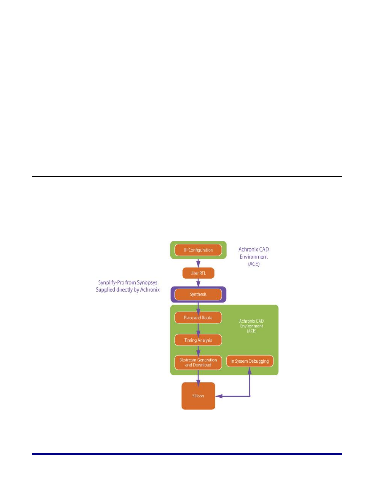
Achronix CAD Environment (ACE) Software
Achronix provides the ACE Software together with an Achronix-optimized version of
Synplify-Pro from Synopsys. You will need a node-locked or floating version of the license to
use the ACE Software for development. You will find more details about installation and use
in the “Development Environment Setup” chapter.
Figure 1 shows the ACE Development Environment.
Figure 1: ACE Development Environment
12 UG034, July 1, 2014
Page 13
13
Chapter 2 – General Description
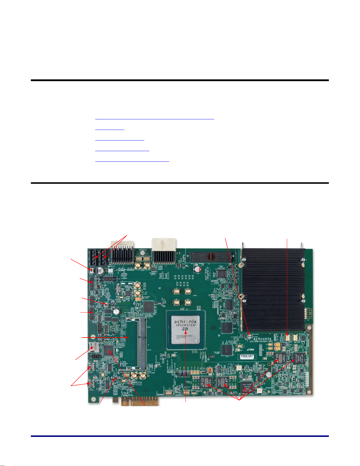
12 V Main and Auxiliary
Power Supply Connectors
JTAG Header for
Bitporter Pod
Connectivity
Board Power
On/Off Switch
FPGA Soft
Reset Switch
Micro SD
Card Slot
SPI Flash
Memory on flip
side of board
(Not shown)
Programming
Header
Microcontroller
Speedster22i
HD1000 FPGA
USB
Connectors
Power
Regulators
Configuration related
LEDs
Configuration related
DIP switches
FPGA Configuration
Hard Reset Switch
In this chapter, you will learn the following about the ACX-BRD-HD1000-100G Development
Board:
ACX-BRD-HD1000-100G Development Board
Use Modes
On-board Memory
On-Board Controller
Board-specific Design Issues
ACX-BRD-HD1000-100G Development Board Picture
The development board has a PCIe form-factor with an 8” (203.2mm) width. It also has
dedicated power connectors. Figure 2 shows the ACX-BRD-HD1000-100G development
board with many of the key components annotated.
UG034, July 1, 2014
Figure 2: ACX-BRD-HD1000-100G Development Board Picture
Page 14
Use Modes
This section describes the standalone and in-system (or “plug-in”) use modes for the
development board. In both modes, you must provide power to the board through the
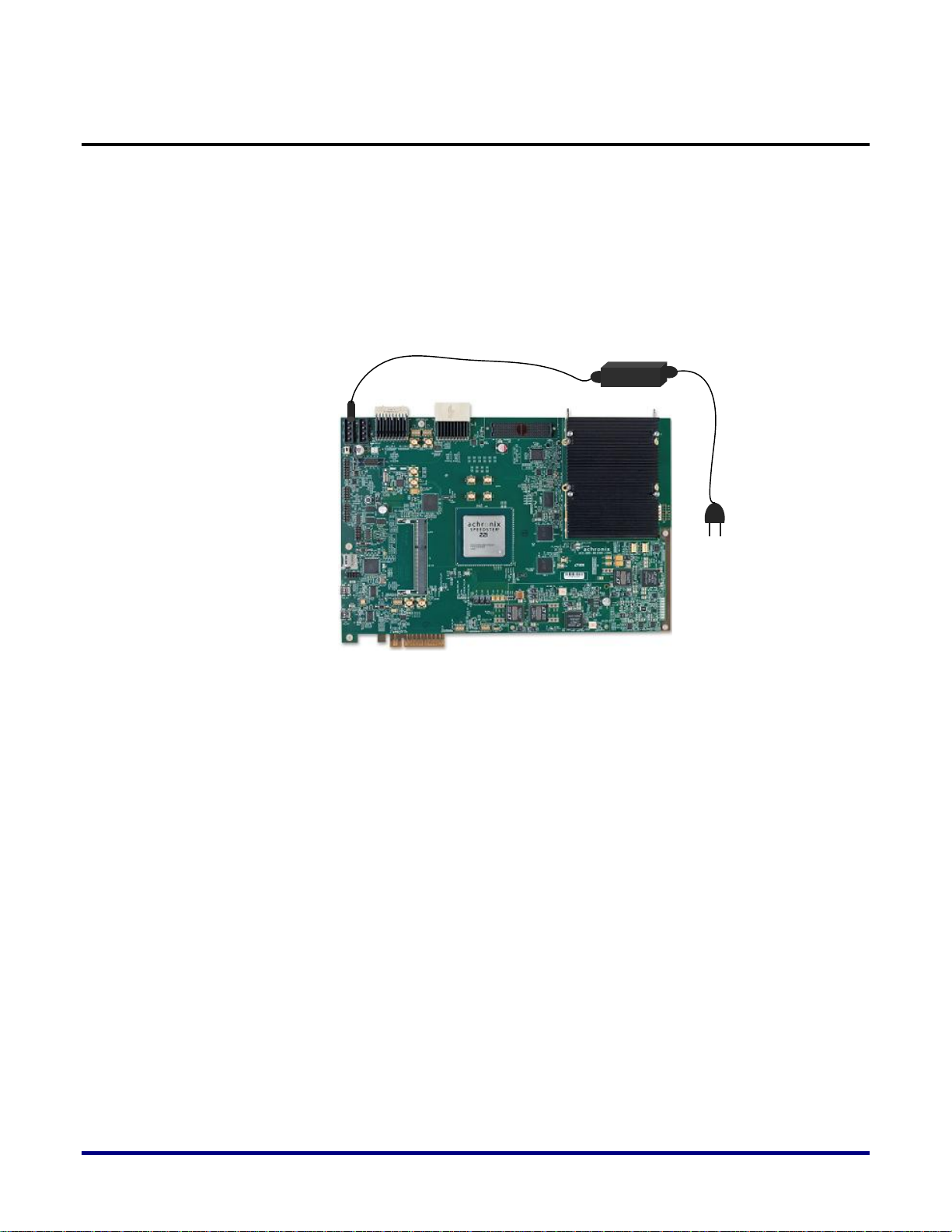
dedicated power connectors using an external power supply.
Standalone Mode
In this mode, the development board is placed on a bench, with control and data signals
coming from the surrounding interfaces, which may include the Atmel microcontroller, DIP
switches, SMAs etc. This mode is shown in Figure 3.
Figure 3: Standalone Use Mode
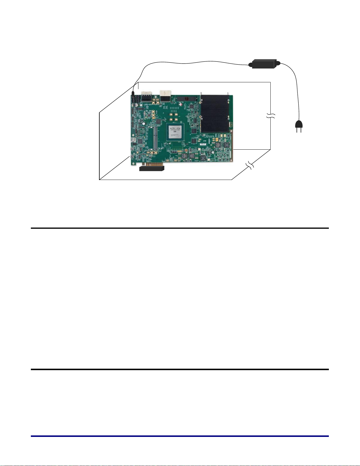
In-system (Plug-in) Mode
The development board is inserted into a PCIe Gen3 x8 slot of a PC. In addition to the
capabilities highlighted in the standalone mode, you may provide data traffic over the PCIe
interface in this mode, assuming you configure the PCIe interface of the FPGA appropriately.
This mode is shown in Figure 4.
Note: You will still need to provide power using an external power supply, rather than the PCIe
connector, and the dedicated power connectors on the board. Additional connectors on the PC power
supply will be sufficient.
14 UG034, July 1, 2014
Page 15
15
PCIe Plug In Card
Power Supply
On-Board Memory
The development board has the following memories available for system design.
A 204-pin SO-DIMM DDR3 module with 2.133 Gb/s performance.
To use as the primary off-chip memory for all applications. This supplements the
on-chip BRAM.
To serve as a demonstration of the embedded DDR3 controller capability.
A DDR3 device (2 Gb @ 1066 MHz) soldered on the board which you can use at 2.133
Gb/s performance.
Two RLDRAM3 (each 16 Mb x 36 for a total of 576 Mb @ 1066 MHz)
A QDR2+ device (2 Mb x 36 = 72 Mb @ 633 MHz) which you can use for high-
bandwidth, low-latency, random-access requirements such as classification and policy
lookup in networking applications.
An SPI Flash device which you can use to store configuration bitstreams on board.
On-Board Controller
Figure 4: In-System Use Mode
The development board comes equipped with an on‐board, Atmel ATmega2560 AVR
microcontroller. You can use this microcontroller to perform the following tasks:
Control power sequencing of the board and any connected peripherals.
Measure the temperature captured via the on‐chip temp diode of the HD1000 FPGA.
Monitor power consumption of some of the key functional blocks.
SerDes
UG034, July 1, 2014
Page 16

IOs
BRAM
Fabric
Take appropriate corrective action by the embedded control software.
Board-Specific Design Issues
The development board is optimized for Networking applications. As such, Achronix has
configured the SerDes and the IOs at specific pins on the HD1000 device. You must maintain
these in any changes that you make to the device as you work on your system development.
Achronix has made this easy for you through a template for ACE that you can use as a tool to
avoid inadvertent changes to the configuration.
You must also maintain the clocking structure implemented on the board for any changes
that you make while using the board as a development platform. For your new designs, you
may use the flexibility provided by the HD1000 to implement your own clocking schemes.
16 UG034, July 1, 2014
Page 17

17
Chapter 3 – Development Environment
Setup
In this chapter, you will learn how to perform the following tasks:
Installing the ACE and Synopsys software and their licenses
Setting up the ACX-BRD-HD1000-100G Development Board
Getting started
Downloading a design
Installing the ACE and Synopsys software and their licenses
You need to perform the following steps to use the ACE Software development environment:
1. Download the required files. Typically, you will choose only ONE of the following
environments:
a. Windows Client, Windows Node-locked license
b. Windows Client, Windows Floating license server
c. Windows Client, Linux Floating license server
d. Linux Client, Linux Node-locked license
e. Linux Client, Linux Floating license server
f. Linux Client, Windows Floating license server
2. Install your licenses e-mailed to you by Achronix on the license server
3. Modify the license servers for Floating licenses only (cases b, c, e, and f)
4. Run the license servers (Not needed for case ’a’ – Windows Node-locked)
5. Set the Client machine environment variables
6. Run the software
Figure 5 shows the Software development environment. You will need to network the Client
machine(s) and the license server.
UG034, July 1, 2014
Page 18
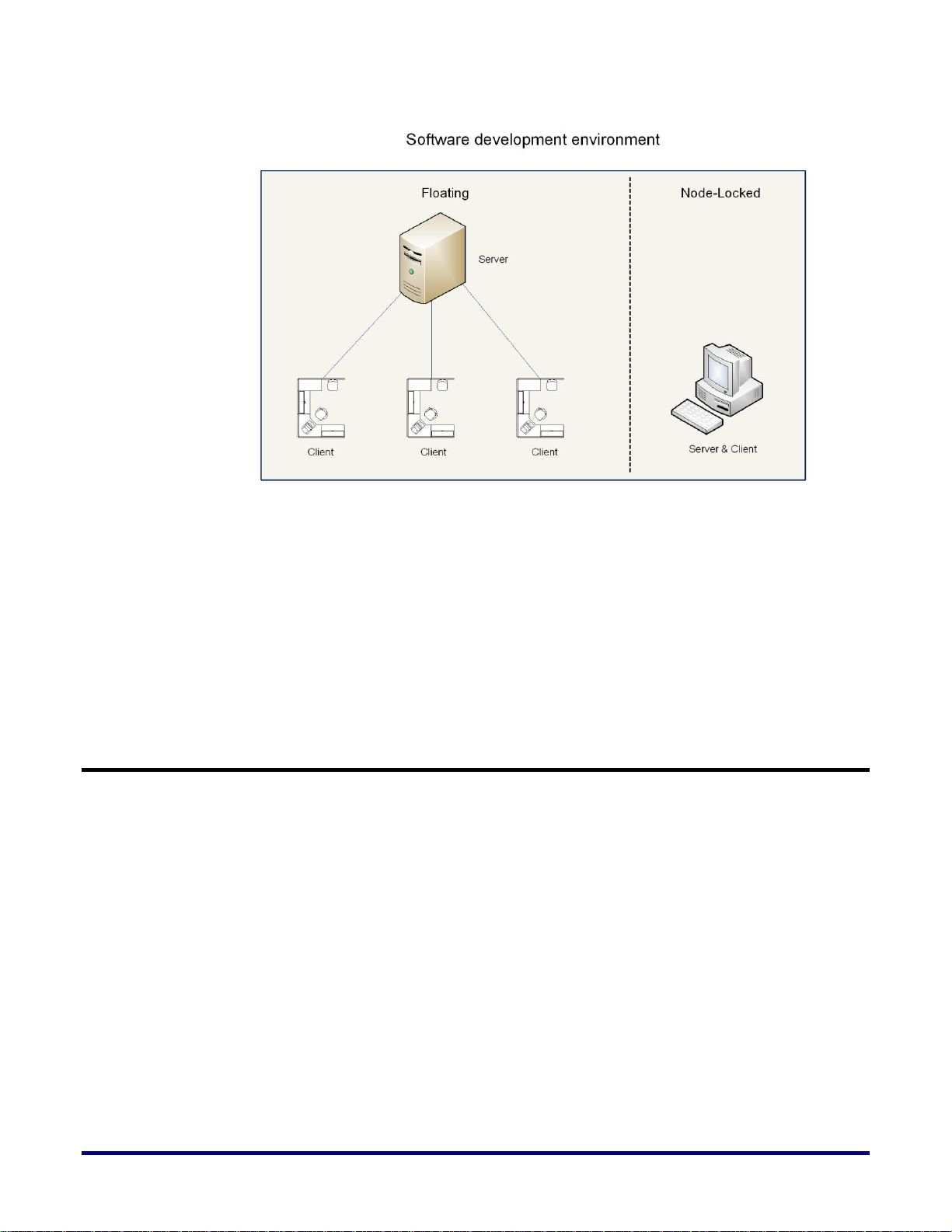
Figure 5: Software Development Environment
For more details on Steps 1 through 6 refer to the Achronix Software & License User Guide
(UG002).
Running the software
You are now ready to run the software on your client machine. Run the executable file to
start using ACE.
For more information, please refer to the Achronix Software & License User Guide (UG002).
Setting up the ACX-BRD-HD1000-100G Development Board
Depending on your requirements, choose either the standalone mode or the in-system (plugin) mode of operation for the board. This guide will discuss both modes.
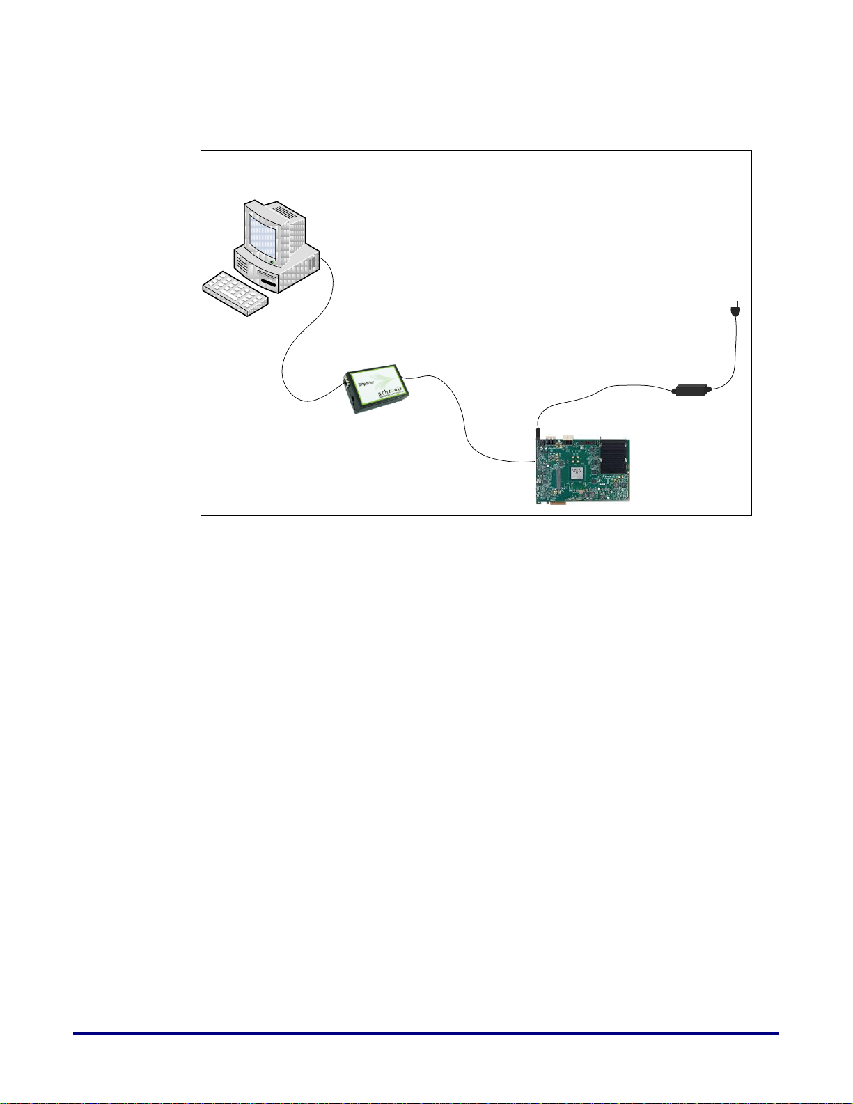
Standalone Mode
You need to connect the development PC and supply power to the board using an external
power source. The connections are shown in Figure 6.
Connecting the Development PC
The development PC is connected to the board using a JTAG ribbon cable that connects to the
USB port on the PC and the JTAG header on the board. The cable (bitporter cable) is
provided with the kit.
Connecting the Power Supply
Although the individual components on the board use different voltage levels, each of these
is generated on the board using a single 12V power supply input.
18 UG034, July 1, 2014
Page 19
19
Standalone Board Connections
USB Cable
JTAG Ribbon Cable
Development PC (Client)
Bitporter Pod
Power Supply
Development Board
Figure 6: Standalone Board Connections
In-system Mode
You need to plug the development board into an available PCIe x8 slot of the development
PC. You need to leave the adjacent slot vacant to accommodate the clearance requirements
for the component side of the board. Figure 7 shows the connections for this mode.
Connecting the Power Supply
Although the individual components on the board use different voltage levels, each of these
is generated on the board using a single 12V power supply input. You may use a spare 12V
supply connector from the development PC power supply.
UG034, July 1, 2014
Page 20
In-System Board Connections
USB Cable
JTAG Ribbon Cable
Development PC (Client)
Bitporter Pod
PCIe Slot Connection
Power Supply
Getting started
Power Sequencing
The power sequencing on the board is preconfigured. After you connect the power supply
and the power good LED (D1) is a steady red, turn on the SW4 switch. The board will
automatically power up all the components in the right order.
Initialization
The devices on the board are controlled either by the ATmega2560 controller or by the
HD1000. Both of these devices can also serve as I2C masters. The HD1000 is the default
master.
The board comes pre-configured for you to get started. Once the power is in place on the
board, a set of LEDs will light up. Please refer to the Quickstart Guide for details on default
power-up behavior.
Note: This guide will assume that your initial efforts will be in the standalone mode and these LEDs
will be easily visible. If you are using the in-system mode, you may not be able to see some of the board
indicators as clearly as in the standalone mode.
Figure 7: In-System Board Connections
Downloading a Design
20 UG034, July 1, 2014
Typically, you need to perform the following steps to download a design to the board and
start debugging your application.
Configure the board for the appropriate bitstream source
Page 21

21
Connect the development PC
Configure the HD1000 and Run the Application
There are three sources currently supported for the FPGA bitstream:
1. JTAG download through BitPorter Pod of bitstream on the development PC
2. SPI Flash
3. A Secure Digital (MicroSD) card
Configuring the Board for the Appropriate Bitstream Source
The board is preconfigured to accept the bitstream from the JTAG interface. Table 1 shows
the shunt positions for J31 to enable the other modes.
Connecting the Development PC
1. Connect the Bitporter pod using the ribbon cable to the development board (J11).
2. Power up the board.
3. Connect the Bitporter pod using the USB port to the development PC.
Configuring the HD1000 and Running the Application
You can configure the FPGA using one of three modes:
1. JTAG
2. Serial
3. CPU
Use jumper J31 and a shunt to select the mode as shown in Table 1. Figure 8 shows the
sources for the bitstream for these modes.
UG034, July 1, 2014
Page 22

CPU x8 Mode
Programming
SPI Flash
Programming
SD CARD
JTAG
Programming
Shunt Position
Configuration Mode
Bitstream Source
OPEN
JTAG
Development PC
2 & 4
Serial
FLASH
2 & 3
CPU
MicroSD
HD1000 (U33)
Connection
Signal Name
Pin
Through
Signal Name
Pin
CONFIG_MODESEL0
L17
SW7
CFG_MS0
1
CONFIG_MODESEL1
L18
CFG_MS1
2
CONFIG_MODESEL2
J17
CFG_MS2
3
CONFIG_SYS_CLK_BYPASS
N18
SCLK_BYP
4
CONFIG_CLKSEL
M17
CFG_CLKSL
5
PROGRAM_ENABLE0
K15
PRG_EN0
6
PROGRAM_ENABLE1
M19
PRG_EN1
7
STAP_SEL
L19
STAP_SEL
8
Figure 8: ACX-BRD-HD1000-100G Board Configuration Modes
Table 1: ACX-BRD-HD1000-100G Board Configuration Mode (J31)
22 UG034, July 1, 2014
Table 2 shows the FPGA configuration pins for the all the modes and their connections.
Table 2: HD1000 Configuration Mode Pins and their Connections
Page 23

23
HD1000 (U33)
Connection
BYPASS_CLR_MEM
J18
SW8
HDR_BYPASS_CLR_MEM
1
CONFIG_SCRUBBING_ENABLE
K19
HDR_CFG_SCR_ENABLE
2
CONFIG_SCRUB_SINGLE_ERR
J20
TP97
CONFIG_SCRUB_MULTIPLE_ERR
M20
TP99
CORE_TESTIN1
K20
TP98
TEMP_DIODE_N
R38
U37
GND
2
TEMP_DIODE_P
R39
DXP
3
CONFIG_RSTN
J14
U96
Y
4
CONFIG_STATUS
M16
Q8
See Note
1
CONFIG_DONE
J16
Q9
1
TDI
K17
J19
1 TDO
K16 4
TMS
J19
J12
2
TRSTN
L16
J11
A_TRST_N
1
TCK
J13
A_TCK 9 SDI
L13
U29
F_CFG_DQ0
10
SD3
L14
F_CFG_DQ1
9
SD2
M13
F_CFG_DQ2
7
SD1
M14
F_CFG_DQ3
6
SD0
N14
F_CFG_DQ4
4
HOLDN
K13
F_CFG_DQ5
12
CSN3
N19
U23
F_CFG_DQ6
6
CSN2
N17
F_CFG_DQ7
4
CSN1
J15
CSN0
N20
U23
F_CFG_CSN
7
CPU_CLK
K18 9
SCK
N13
UA2
3
START_CONFIG_STARTUP
K14
SW8
HDR_CONFIG_STARTUP
EFUSE_PROG
T14
TP100
EDM
B9
TP103
READ_STATE_ERR
N16
Q2
See Note
1
Note: Q8, Q9, and Q2 drive status indicator LEDs: D1, D2, and D6. CSN1 is unused.
Pin Name on HD
1000 (U33)
x1 Boot from Flash
(Serial Mode) - EFC
CPU Mode
SDI
DQ0
Serial data output to FLASH memory
SDO3
DQ1
Input of config data from FLASH
SDO2
DQ2
Input of config data from FLASH
SDO1
DQ3
Input of config data from FLASH
SDO0
DQ4
Input of config data from FLASH
HOLDN
DQ5
Hold output to FLASH
CSN3
DQ6
Active-low chip select
CSN2
DQ7
Active-low chip select
CSN1
UNUSED
Active-low chip select
CSN0
Active-low chip select
Table 3 shows the configuration pin descriptions and their functions for HD1000
configuration.
UG034, July 1, 2014
Table 3: HD1000 Pins and their Descriptions for Configuration
Page 24

Pin Name on HD
1000 (U33)
x1 Boot from Flash
(Serial Mode) - EFC
CPU Mode
CPU_CLK
CPU CLOCK
--
CONFIG_RSTN
Active-low configuration reset
CONFIG_DONE
Open-drain configuration done output
CONFIG_STATUS
Open-drain SRAM initialization complete output
CONFIG_MODESEL
[2:0]
Must be : ‘100’
Must be : ‘010’
CONFIG_SYSCLK_
BYPASS
Bypass configuration sys
clock : Don’t Care
Bypass configuration sys clock : Set to ‘0’
CONFIG_CLKSEL
Select Configuration Clock : Set to ‘0’
JTAG
The development PC provides the bitstream source to configure the HD1000. You download
this to the board using the JTAG connection, the Bitporter pod and either the ACE
environment or a command line interface.
Serial
In this mode, the FPGA is configured from the Serial Flash (U78).
CPU
In this mode, the FPGA is configured from the MicroSD card.
FLASH Programming
You can program the Flash using the JTAG interface with the jumper (J31) position at 1&2.
Once you program the FPGA and see the CONFIG_DONE LED light green, this means that
the configuration has successfully completed and that the part has transitioned to user mode.
At this point, you can run your application as desired.
24 UG034, July 1, 2014
Page 25

25
Chapter 4 – Interfaces
In this chapter you will learn about the interfaces that are available on the HD1000 FPGA and
also the ones available on the development board. This guide covers details of the interfaces
available on the development board. The interfaces on the HD1000 FPGA are included for
completeness. Figure 9 shows the interfaces available on the HD1000 FPGA.
UG034, July 1, 2014
Page 26

HD1000 FPGA Interfaces
BLN
BLN
BLN
CNFG
BANK EAST-CENTRE
(BYTE 0-12)
BANK EAST-NORTH
(BYTE 0-12)
BANK EAST-SOUTH
(BYTE 0-12)
BLN
BLN
BLN
BANK WEST-CENTRE
(BYTE 0-12)
BANK WEST-NORTH
(BYTE 0-12)
BANK WEST-SOUTH
(BYTE 0-12)
WEST-NORTH
PLL
SERDES - TOP
SERDES - BOTTOM
GPIO
EAST-NORTH
PLL
EAST-SOUTH
PLL
HD1000 FPGA
TOP VIEW
WEST-SOUTH
PLL
SFLASH
64Mbit
ATMEL MICRO
256KB 8MHZ
FTDI CHIP
FT232RL
QDR II +
2MbX36
FMC
CONNECTOR
2Gb DISCRETE
DDR3 1x16 BIT
RLDRAM-3
16MbX36
RLDRAM-3
16MbX36
8
SD CARD
HEADER
SMA
CLK OSCILLATOR
PCI EXPRESS LLC
(X8)
16
72
Width
Expansion
USB 2.0 B
JTAG HEADER
JTAG
204 - SO-DIMM
X64
USB 2.0 B
SPI
SMA
36
64
x8
SYNTHESIZER CLK
12
31 30 29 28 27 26 25 24 23 22 21 20 19 18 17 16 15 14 13 12 11 10 9 8 7 6 5 4 3 2 1 0
31 30 29 28 27 26 25 24 23 22 21 20 19 18 17 16 15 14 13 12 11 10 9 8 7 6 5 4 3 2 1 0
CFP
10
10
U22
U33
J1/J2
J41
J11
U41
U35
J14
J35
U54
U31/U36
U21
J3
FTDI CHIP
FT232RL
FMC-Serdes Group
INTERLAKEN
HEADER
J20
J28
FMC CLK
RESET1
SYNTHESIZER CLK
S1
FMC CLK
26 UG034, July 1, 2014
Figure 9: HD1000 FPGA Interfaces
Page 27

27
ACX-BRD-HD1000-100G Development Board Interfaces
Figure 10 shows the interfaces available on the development board. These interfaces are
discussed in more detail in the following sections:
Networking and Communications Interfaces
System Interfaces
Controller Interfaces
Memory Interfaces
User Interfaces
Figure 10: ACX-BRD-HD1000-100G Development Board Interface Overview
UG034, July 1, 2014
Page 28

Figure 11 below shows all of these different interfaces on the development board.
CFP Cage
Interlaken AirMax
Connector Pair
400-Pin FMC
Expansion Port
PCI Express Connector
USB Connector for
Microcontroller Interface
USB Connector for
FPGA Interface
72Mb QDRII+
Module
204-Pin DDR3
SO-DIMM
2 RLDRAM3 modules
(16Mbx36 each)
2Gb DDR3
Module
QTE
SMAs
FPGA Clk
Bank SMAs
SerDes Clk
SMAs
SerDes Tx/Rx
SMAs
Digilent
Connector
Figure 11: ACX-BRD-HD1000-100G Development Board Interface Locations
Networking and Communications Interfaces
You can develop your networking and communications applications using the following
interfaces:
CFP cage for 100GE line interface
Interlaken interface (AirMax connector pair)
FMC expansion port (HPC)
CFP Cage for 100GE Line Interface
The CFP interface provides you with the primary high-speed data interface for the board.
You can use this to evaluate the 10G/40G/100G capabilities of the HD1000. For the data path,
you have a total of 200 Gb/s bandwidth (100 Gb/s Tx and 100 Gb/s Rx). You can use the
following Ethernet modules for insertion:
1. 1 x 100 G
2. 2 x 40 G
3. 10 x 10 G
28 UG034, July 1, 2014
Page 29

29
The CFP cage is directly connected to the ten bidirectional 12.5 G SerDes lanes. These are
Signal Name
SerDes No
Pin on HD1000 (U33)
CFP1_RX_P0
8 – 9
F19
CFP1_RX_N0
E19
CFP1_TX_P0
B19
CFP1_TX_N0
C19
CFP1_RX_P1
G20
CFP1_RX_N1
F20
CFP1_TX_P1
A20
CFP1_TX_N1
B20
SERDES_CFP1_CLK4_P
M28
SERDES_CFP1_CLK4_N
N28
CFP1_RX_P2
10 – 11
F21
CFP1_RX_N2
E21
CFP1_TX_P2
B21
CFP1_TX_N2
C21
CFP1_RX_P3
G22
CFP1_RX_N3
F22
CFP1_TX_P3
A22
CFP1_TX_N3
B22
SERDES_CFP1_CLK5_P
M29
SERDES_CFP1_CLK5_N
N29
CFP1_RX_P4
12 – 13
F23
CFP1_RX_N4
E23
CFP1_TX_P4
B23
CFP1_TX_N4
C23
CFP1_RX_P5
G24
CFP1_RX_N5
F24
CFP1_TX_P5
A24
CFP1_TX_N5
B24
SERDES_CFP1_CLK3_P
J28
SERDES_CFP1_CLK3_N
K28
CFP1_RX_P6
14 – 15
F25
CFP1_RX_N6
E25
CFP1_TX_P6
B25
CFP1_TX_N6
C25
CFP1_RX_P7
G26
CFP1_RX_N7
F26
CFP1_TX_P7
A26
CFP1_TX_N7
B26
SERDES_CFP1_CLK2_P
J29
SERDES_CFP1_CLK2_N
K29
CFP1_RX_P8
16 – 17
F27
CFP1_RX_N8
E27
CFP1_TX_P8
B27
CFP1_TX_N8
C27
CFP1_RX_P9
G28
designated SerDes Bottom 8 – 17 in Figure 9. Table 4 shows the pin assignment for the CFP
interface.
Table 4: ACX-BRD-HD1000-100G CFP Interface Pins
UG034, July 1, 2014
Page 30

Signal Name
SerDes No
Pin on HD1000 (U33)
CFP1_RX_N9
F28
CFP1_TX_P9
A28
CFP1_TX_N9
B28
SERDES_CFP1_CLK1_P
M31
SERDES_CFP1_CLK1_N
N31
Signal Name
SerDes No
Pin on HD1000
(U33)
Pin on Header
(J1)
INTERLAKEN_TX_P0
20 – 21
BJ31
A7
INTERLAKEN_TX_N0
BK31
B7
INTERLAKEN_TX_P1
BK32
D6
INTERLAKEN_TX_N1
BL32
E6
INTERLAKEN1_CLK6_P
BC28
NA
INTERLAKEN1_CLK6_N
BB28
NA
INTERLAKEN_TX_P2
22 – 23
BK33
D8
INTERLAKEN_TX_N2
BJ33
E8
INTERLAKEN_TX_P3
BL34
A9
INTERLAKEN_TX_N3
BK34
B9
INTERLAKEN1_CLK5_P
BC29
NA
INTERLAKEN1_CLK5_N
BB29
NA
INTERLAKEN_TX_P4
24 – 25
BK35
A3
INTERLAKEN_TX_N4
BJ35
B3
INTERLAKEN_TX_P5
BK36
D2
INTERLAKEN_TX_N5
BL36
E2
INTERLAKEN1_CLK4_P
AY31
NA
INTERLAKEN1_CLK4_N
AW31
NA
INTERLAKEN_TX_P6
26 – 27
BK37
D4
INTERLAKEN_TX_N6
BJ37
E4
INTERLAKEN_TX_P7
BK38
A5
INTERLAKEN_TX_N7
BL38
B5
INTERLAKEN1_CLK2_P
AY32
NA
INTERLAKEN1_CLK2_N
AW32
NA
INTERLAKEN_TX_P8
28 – 29
BK39
G5
INTERLAKEN_TX_N8
BJ39
H5
INTERLAKEN_TX_P9
BK40
G3
INTERLAKEN_TX_N9
BL40
H3
INTERLAKEN1_CLK3_P
BC31
NA
Interlaken Interface (AirMax Connector Pair)
The Interlaken interface provides a secondary high-speed datapath. You can use this to
enable interoperation with other packet-processing devices such as ASICs and/or Network
Processors. In such operation, you can implement certain decision making functions on the
the HD1000 prior to presenting the Ethernet packet to the Network Processing Unit (NPU).
The board uses dual AirMax connectors (one for Tx, the second for Rx). The interface
supports 12 x 11.3 Gb/s bandwidth.
Figure 11 shows the Interlaken Interface, and Table 5 and Table 6, the associated pins. These
are designated SerDes Top 20 – 31 in Figure 9 for the HD1000.
Table 5: ACX-BRD-HD1000-100G Interlaken Transmitter Interface Pins
30 UG034, July 1, 2014
Page 31

31
Signal Name
SerDes No
Pin on HD1000
(U33)
Pin on Header
(J1)
INTERLAKEN1_CLK3_N
BB31
NA
INTERLAKEN_TX_P10
30 – 31
BJ41
J4
INTERLAKEN_TX_N10
BK41
K4
INTERLAKEN_TX_P11
BL42
G1
INTERLAKEN_TX_N11
BK42
H1
INTERLAKEN1_CLK1_P
BC32
NA
INTERLAKEN1_CLK1_N
BB32
NA
INTERLAKEN1_TX_CLK_P
NA
A1
INTERLAKEN1_TX_CLK_N
NA
B1
Signal Name
SerDes No
Pin on HD1000
(U33)
Pin on
Receptacle (J2)
INTERLAKEN_RX_P0
20 – 21
BF31
A7
INTERLAKEN_RX_N0
BG31
B7
INTERLAKEN_RX_P1
BE32
D6
INTERLAKEN_RX_N1
BF32
E6
INTERLAKEN1_CLK6_P
BC28
NA
INTERLAKEN1_CLK6_N
BB28
NA
INTERLAKEN_RX_P2
22 – 23
BF33
D8
INTERLAKEN_RX_N2
BG33
E8
INTERLAKEN_RX_P3
BE34
A9
INTERLAKEN_RX_N3
BF34
B9
INTERLAKEN1_CLK5_P
BC29
NA
INTERLAKEN1_CLK5_N
BB29
NA
INTERLAKEN_RX_P4
24 – 25
BF35
A3
INTERLAKEN_RX_N4
BG35
B3
INTERLAKEN_RX_P5
BF36
D2
INTERLAKEN_RX_N5
BE36
E2
INTERLAKEN1_CLK4_P
AY31
NA
INTERLAKEN1_CLK4_N
AW31
NA
INTERLAKEN_RX_P6
26 – 27
BF37
D4
INTERLAKEN_RX_N6
BG37
E4
INTERLAKEN_RX_P7
BF38
A5
INTERLAKEN_RX_N7
BE38
B5
INTERLAKEN1_CLK2_P
AY32
NA
INTERLAKEN1_CLK2_N
AW32
NA
INTERLAKEN_RX_P8
28 – 29
BF39
G5
INTERLAKEN_RX_N8
BG39
H5
INTERLAKEN_RX_P9
BF40
G3
INTERLAKEN_RX_N9
BE40
H3
INTERLAKEN1_CLK3_P
BC31
NA
INTERLAKEN1_CLK3_N
BB31
NA
INTERLAKEN_RX_P10
30 – 31
BG41
J4
INTERLAKEN_RX_N10
BF41
K4
INTERLAKEN_RX_P11
BE42
G1
INTERLAKEN_RX_N11
BF42
H1
INTERLAKEN1_CLK1_P
BC32
NA
Table 6: ACX-BRD-HD1000-100G Interlaken Receiver Interface Pins
UG034, July 1, 2014
Page 32

Signal Name
SerDes No
Pin on HD1000
(U33)
Pin on
Receptacle (J2)
INTERLAKEN1_CLK1_N
BB32
NA
INTERLAKEN1_RX_CLK_P
NA
A1
INTERLAKEN1_RX_CLK_N
NA
B1
Signal Name
Pin on HD1000 (U33)
Pin on Connector (J3)
CLK_DIR_FMC
AH44
B1
CLK0_M2C_P
BC14
H5
CLK0_M2C_N
BB14
H4
CLK1_M2C_P
BA14
G3
CLK1_M2C_N
AY14
G2
CLK2_M2C_P
AW14
K5
CLK2_M2C_N
AV14
K4
CLK3_M2C_P
AY38
J3
CLK3_M2C_N
AW37
J2
GBTCLK0_M2C_P
D4
GBTCLK0_M2C_N
D5
GBTCLK0_M2C_P
B21
GBTCLK0_M2C_N
B20
FMC_CLK_M2C_P0
AY25
FMC_CLK_M2C_N0
AW25
FMC_CLK_M2C_P1
AY26
FMC_CLK_M2C_N1
AW26
FMC_CLK_M2C_P2
BC25
FMC_CLK_M2C_N2
BB25
FMC_CLK_M2C_P3
BC26
FMC_CLK_M2C_N3
BB26
FMC_CLK_M2C_P4
AY28
FMC_CLK_M2C_N4
AW28
VDDL_PG
D1
POWER_GOOD_M2C
AH45
F1
PRSNT_M2C_L
AJ45
H2
SPD_FMC_SCL
AJ42
C30
SPD_FMC_SDA
AJ43
C31
FMC_TCK
D29
FMC_TDI
D30
FMC_TDO
D31
FMC_TMS
D33
FMC Expansion Port (HPC, J3)
You can use the FMC port to add other circuitry or functionality. Banks East Centre and West
North of the HD1000 provide the IOs for connections to the 400-pin SAMTEC ASP-134485-01
connector (J3) as shown in Figure 11. Table 7 shows the FMC interface pins and their
connections to the HD1000.
Table 7: ACX-BRD-HD1000-100G FMC Interface Pins
32 UG034, July 1, 2014
Page 33

UG034, July 1, 2014
33
Signal Name
Pin on HD1000 (U33)
Pin on Connector (J3)
FMC_TRST_N
D34
FMC_DP_M2C_P0
BF19
C7
FMC_DP_M2C_N0
BG19
C6
FMC_DP_M2C_P1
BE20
A3
FMC_DP_M2C_N1
BF20
A2
FMC_DP_M2C_P2
BF21
A7
FMC_DP_M2C_N2
BG21
A6
FMC_DP_M2C_P3
BE22
A11
FMC_DP_M2C_N3
BF22
A10
FMC_DP_M2C_P4
BF23
A15
FMC_DP_M2C_N4
BG23
A14
FMC_DP_M2C_P5
BE24
A19
FMC_DP_M2C_N5
BF24
A18
FMC_DP_M2C_P6
BF25
B17
FMC_DP_M2C_N6
BG25
B16
FMC_DP_M2C_P7
BE26
B13
FMC_DP_M2C_N7
BF26
B12
FMC_DP_M2C_P8
BF27
B9
FMC_DP_M2C_N8
BG27
B8
FMC_DP_M2C_P9
BE28
B5
FMC_DP_M2C_N9
BF28
B4
FMC_DP_C2M_P0
BK19
C3
FMC_DP_C2M_N0
BJ19
C2
FMC_DP_C2M_P1
BL20
A23
FMC_DP_C2M_N1
BK20
A22
FMC_DP_C2M_P2
BK21
A27
FMC_DP_C2M_N2
BJ21
A26
FMC_DP_C2M_P3
BL22
A31
FMC_DP_C2M_N3
BK22
A30
FMC_DP_C2M_P4
BK23
A35
FMC_DP_C2M_N4
BJ23
A34
FMC_DP_C2M_P5
BL24
A39
FMC_DP_C2M_N5
BK24
A38
FMC_DP_C2M_P6
BK25
B37
FMC_DP_C2M_N6
BJ25
B36
FMC_DP_C2M_P7
BL26
B33
FMC_DP_C2M_N7
BK26
B32
FMC_DP_C2M_P8
BK27
B29
FMC_DP_C2M_N8
BJ27
B28
FMC_DP_C2M_P9
BL28
B25
FMC_DP_C2M_N9
BK28
B24
FMC_LA_CC_P0
AY8
G6
FMC_LA_CC_N0
AY7
G7
FMC_LA_CC_P1
AY6
D8
FMC_LA_CC_N1
AY5
D9
FMC_LA_P2
BA8
H7
FMC_LA_N2
BC8
H8
FMC_LA_P3
BB7
G9
Page 34

34 UG034, July 1, 2014
Signal Name
Pin on HD1000 (U33)
Pin on Connector (J3)
FMC_LA_N3
AW8
G10
FMC_LA_P4
BC7
H10
FMC_LA_N4
AW7
H11
FMC_LA_P5
BB8
D11
FMC_LA_N5
AV7
D12
FMC_LA_P6
AU8
C10
FMC_LA_N6
AU7
C11
FMC_LA_P7
BB6
H13
FMC_LA_N7
BC5
H14
FMC_LA_P8
BE5
G12
FMC_LA_N8
BD5
G13
FMC_LA_P9
AU6
D14
FMC_LA_N9
BA6
D15
FMC_LA_P10
BC6
C14
FMC_LA_N10
BB5
C15
FMC_LA_P11
BF6
H16
FMC_LA_N11
BK6
H17
FMC_LA_P12
AW5
G15
FMC_LA_N12
AV5
G16
FMC_LA_P13
AW6
D17
FMC_LA_N13
AU5
D18
FMC_LA_P14
BH6
C18
FMC_LA_N14
BD6
C19
FMC_LA_P15
BG6
H19
FMC_LA_N15
BG5
H20
FMC_LA_P16
BK5
G18
FMC_LA_N16
BF5
G19
FMC_LA_CC_P17
BJ6
D20
FMC_LA_CC_N17
BJ5
D21
FMC_LA_CC_P18
BF4
C22
FMC_LA_CC_N18
BF3
C23
FMC_LA_P19
BJ4
H22
FMC_LA_N19
BK4
H23
FMC_LA_P20
BH4
G21
FMC_LA_N20
BG4
G22
FMC_LA_P21
BG3
H25
FMC_LA_N21
BD4
H26
FMC_LA_P22
BJ3
G24
FMC_LA_N22
BL4
G25
FMC_LA_P23
BD3
D23
FMC_LA_N23
BE3
D24
FMC_LA_P24
BH2
H28
FMC_LA_N24
BJ2
H29
FMC_LA_P25
BH1
G27
FMC_LA_N25
BF2
G28
FMC_LA_P26
BD2
D26
FMC_LA_N26
BD1
D27
FMC_LA_P27
BK2
C26
FMC_LA_N27
BE2
C27
FMC_LA_P28
BK3
H31
FMC_LA_N28
BE1
H32
FMC_LA_P29
BG2
G30
Page 35

UG034, July 1, 2014
35
Signal Name
Pin on HD1000 (U33)
Pin on Connector (J3)
FMC_LA_N29
BG1
G31
FMC_LA_P30
BB4
H34
FMC_LA_N30
BC3
H35
FMC_LA_P31
BC4
G33
FMC_LA_N31
BA4
G34
FMC_LA_P32
AV3
H37
FMC_LA_N32
BB3
H38
FMC_LA_P33
AW4
G36
FMC_LA_N33
AU3
G37
FMC_HA_CC_P0
AY4
F4
FMC_HA_CC_N0
AY3
F5
FMC_HA_CC_P1
AN10
E2
FMC_HA_CC_N1
AN9
E3
FMC_HA_P2
AP10
K7
FMC_HA_N2
AK10
K8
FMC_HA_P3
AR10
J6
FMC_HA_N3
AT9
J7
FMC_HA_P4
AT10
F7
FMC_HA_N4
AM9
F8
FMC_HA_P5
AK9
E6
FMC_HA_N5
AM10
E7
FMC_HA_P6
AP8
K10
FMC_HA_N6
AR8
K11
FMC_HA_P7
AR9
J9
FMC_HA_N7
AL9
J10
FMC_HA_P8
AM8
F10
FMC_HA_N8
AM7
F11
FMC_HA_P9
AK8
E9
FMC_HA_N9
AK7
E10
FMC_HA_P10
AR6
K13
FMC_HA_N10
AM6
K14
FMC_HA_P11
AN8
J12
FMC_HA_N11
AN7
J13
FMC_HA_P12
AM5
F13
FMC_HA_N12
AK5
F14
FMC_HA_P13
AP6
E12
FMC_HA_N13
AK6
E13
FMC_HA_P14
AU4
J15
FMC_HA_N14
AW3
J16
FMC_HA_P15
AR5
F16
FMC_HA_N15
AL5
F17
FMC_HA_P16
AL7
E15
FMC_HA_N16
AT8
E16
FMC_HA_CC_P17
AN6
K16
FMC_HA_CC_N17
AN5
K17
FMC_HA_P18
AR7
J18
FMC_HA_N18
AT7
J19
FMC_HA_P19
AT6
F19
FMC_HA_N19
AT5
F20
FMC_HA_P20
AE4
E18
Page 36

Signal Name
Pin on HD1000 (U33)
Pin on Connector (J3)
FMC_HA_N20
AE3
E19
FMC_HA_P21
AC4
K19
FMC_HA_N21
AF3
K20
FMC_HA_P22
AJ3
J21
FMC_HA_N22
AF4
J22
FMC_HA_P23
AJ4
K22
FMC_HA_N23
AG4
K23
VADJ_FMC
AP16, AP17, AR17, AT16,
AT17, AU16, AU17, AV17,
AW16, AW17, AE16,
AE17, AF17, AG16, AG17
H40, G39, F40, E39
VREF_A_M2C
AL15 (thru J532)
H1
FMC_HB_CC_P0
AW12
K26
FMC_HB_CC_N0
AW11
K25
FMC_HB_P1
AY12
J25
FMC_HB_N1
AY11
J24
FMC_HB_P2
AT11
F23
FMC_HB_N2
AT12
F22
FMC_HB_P3
BC11
E22
FMC_HB_N3
BC12
E21
FMC_HB_P4
AW10
F26
FMC_HB_N4
BC10
F25
FMC_HB_P5
AU12
E25
FMC_HB_N5
AU11
E24
FMC_HB_CC_P6
AN12
K29
FMC_HB_CC_N6
AN11
K28
FMC_HB_P7
AM12
J28
FMC_HB_N7
AK11
J27
FMC_HB_P8
AK12
F29
FMC_HB_N8
AL11
F28
FMC_HB_P9
BB11
E28
FMC_HB_N9
AV11
E27
FMC_HB_P10
AP12
K32
FMC_HB_N10
AR11
K31
FMC_HB_P11
AM11
J31
FMC_HB_N11
AR12
J30
FMC_HB_P12
BA10
F32
FMC_HB_N12
BC9
F31
FMC_HB_P13
BA12
E31
FMC_HB_N13
BB12
E30
FMC_HB_P14
BB9
K35
FMC_HB_N14
AW9
K34
FMC_HB_P15
BB10
J34
FMC_HB_N15
AU10
J33
FMC_HB_P16
AV9
F35
FMC_HB_N16
AU9
F34
FMC_HB_CC_P17
AY10
K38
FMC_HB_CC_N17
AY9
K37
FMC_HB_P18
BH8
J37
36 UG034, July 1, 2014
Page 37

37
Signal Name
Pin on HD1000 (U33)
Pin on Connector (J3)
FMC_HB_N18
BJ8
J36
FMC_HB_P19
BF8
E34
FMC_HB_N19
BD8
E33
FMC_HB_P20
BK8
F38
FMC_HB_N20
BD7
F37
FMC_HB_P21
BJ7
E37
FMC_HB_N21
BE7
E36
VIO_B_FMC
AY16, AY17, BA17, BB16,
BB17
K40, J39
VREF_B_M2C
AR15 (thru J531)
K1
Signal Name
SerDes No
Pin on HD1000
(U33)
Pin on PCIe x8
Finger (J4)
PCIE_RXP0
0
F11
B45
PCIE_RXN0
E11
B46
PCIE_TXP0
B11
A47
PCIE_TXN0
C11
A48
PCIE_RXP1
1
G12
B41
PCIE_RXN1
F12
B42
PCIE_TXP1
A12
A43
PCIE_TXN1
B12
A44
PCIE_RXP2
2
F13
B37
PCIE_RXN2
E13
B38
PCIE_TXP2
B13
A39
PCIE_TXN2
C13
A40
PCIE_RXP3
3
G14
B33
PCIE_RXN3
F14
B34
PCIE_TXP3
A14
A35
PCIE_TXN3
B14
A36
PCIE_RXP4
4
F15
B27
PCIE_RXN4
E15
B28
PCIE_TXP4
B15
A29
System Interfaces
The ACX-BRD-HD1000-100G board has the following system interfaces:
PCI Express
USB
JTAG
PCI Express
You can use the PCIe connector to plug into a development PC where the data is provided
over the PCIe interface. The Gen 3, x8 interface supports 2 x64 Gb/s throughput (64 Gb/s Rx,
64 Gb/s Tx). You cannot provide power to the board over the PCIe interface. Figure 11 shows
the dedicated PCIe pins on the HD1000. These are designated SerDes Bottom 0 – 7 in Figure
9. Table 8 shows the pins on the HD1000 and their connections to the PCIe edge connector.
Table 8: ACX-BRD-HD1000-100G PCIe Interface Pins
UG034, July 1, 2014
Page 38
Signal Name
SerDes No
Pin on HD1000
(U33)
Pin on PCIe x8
Finger (J4)
PCIE_TXN4
C15
A30
PCIE_RXP5
5
G16
B23
PCIE_RXN5
F16
B24
PCIE_TXP5
A16
A25
PCIE_TXN5
B16
A26
PCIE_RXP6
6
F17
B19
PCIE_RXN6
E17
B20
PCIE_TXP6
B17
A21
PCIE_TXN6
C17
A22
PCIE_RXP7
7
G18
B14
PCIE_RXN7
F18
B15
PCIE_TXP7
A18
A16
PCIE_TXN7
B18
A17
PCIE_MAXOUT_P
(SerDes Ref Clock)
M25
M26
J25
J26
Selected using U57
PCIE_MAXOUT_N
(SerDes Ref Clock)
N25
N26
K25
K26
USB Connector (U54)
HD1000 (U33)
Signal Name
Pin
Signal Name
Pin
D+
3
UART_TXD
BB50
D-
2
UART_RXD
BB51
USB Connector (U41)
Microcontroller – Atmega2560 (U35)
Signal Name
Pin
Signal Name
Pin
D+
3
AVR_RXD
2
D-
2
AVR_TXD
3
USB (U54, U41)
There are two USB connectors on the board, U54 and U41. You can use the USB (U54)
interface for communicating with the board. This interface lets you access the JTAG interface
pins on the HD1000. In addition, information is transferred from the board to the
development PC. You can use this information for further debug, development or application
actions. These two USB connectors can be seen in Figure 11. The HD1000 (U33) controls the
communication between the USB port (U54) and the development PC. The development PC
and the MCU (U35) communicate over U41. Table 9 and Table 10 show the connections
between the U54 and HD1000 and U41 and the MCU.
Table 9: ACX-BRD-HD1000-100G USB Interface Connections (HD1000)
Table 10: ACX-BRD-HD1000-100G USB Interface Connections (MCU)
38 UG034, July 1, 2014
Page 39

39
JTAG Header (J11)
Connection
Signal
Pin
Through
Signal Name
Pin
A_TRST_N
1
FMC Connector (J3)
FMC_TRST_N
D34
A_TMS
7
FMC _TMS
D33
A_TCK
9
FMC _TCK
D29
A_TDO
5
Jumper (J54)
A_TDO
1
A_TDI
3
Jumper (J19)
FPGA_TDI
2
J11
J12 J33 J40 J30
J19
J54
J32
J39
J27
J17
JTAG (J11)
You can use the JTAG interface for communicating with the board. This interface lets you
access the JTAG interface pins on the HD1000. In addition, information is transferred from
the board to the development PC. The header can be seen in Figure 2. You can use this
information for further debug, development or application actions. The signal pins for the 14pin are listed in Table 11.
Table 11: ACX-BRD-HD1000-100G JTAG Header (J11) Pins.
The JTAG header pin A_TDI drives the FPGA_TDI pin TBD on the HD1000. This is daisy
chained using the TDO and TDI pins and jumpers to the RLDRAM3 devices (U31, U36), the
QDR2 device (U22) and the FMC connector (J3). The TDO signal from the FMC connector
goes back to the JTAG header (J11) to complete the daisy chain.
The daisy chain is shown in Figure 12.
Figure 12: ACX-BRD-HD1000-100G JTAG Daisy Chain
Note: Figure 12 shows only the logical connection for application development. Relevant voltage
levels are driven on the board by additional circuitry.
UG034, July 1, 2014
Page 40

Controller Interfaces
Microcontroller – Atmega2560 (U35)
Connection
Interface
Pin Name
Pin
Interface
Signal Name
Pin
SD
PA1/AD1
77
Micro-SD Socket
SD_CLK
5
PA2/AD2
76
SD_DAT3
2
PA3/AD3
75
SD_DAT2
1
PA4/AD4
74
SD_DAT1
8
PA5/AD5
73
SD_DAT0
7
PA6/AD6
72
SD_CMD
3
SPI
SCK/PCINT1/PB1
20
Header (J20)
AVR_SCK
1
MISO/PCINT3/PB3
22
AVR_PDO
3
MOSI/PCINT2/PB2
21
AVR_PDI
9
SS_N/PCINT0/PB0
19
AVR_SS
6
Header
PF4/ADC4/TCK
93
Header (J43)
AVR_TCK
1
PF5/ADC5/TMS
92
AVR_TMS
5
PF6/ADC6/TDO
91
AVR_TDO
3
PF7/ADC7/TDI
90
AVR_TDI
9
The Atmel Atmega2560 (U35) controller has the following interfaces for performing several
tasks on the development board.
Serial interface to the USB port for communications with the development PC
SD card for uploading bitstreams to the HD1000
SPI for SFLASH memory control
Header for configuration
HD1000 for configuration
These interfaces are shown in Figure 11. Table 12 shows the relevant pins and their
connections.
Table 12: ACX-BRD-HD1000-100G Microcontroller Interfaces and their Connections
Memory Interfaces
The board has five off-chip memory interfaces in addition to the removable SD and the
SFLASH.
One 204-pin SO-DIMM socket (4 GB)
One DDR3 device (2 Gb)
Two RLDRAM3 devices (2 x 16 Mbx36)
One QDR2+ device (72 Mb)
Figure 11 shows the off-chip memory interfaces for the HD1000.
SO-DIMM Socket (J41)
You can use a standard 204-pin DDR3 SO-DIMM (up to 4 GB, 2133 MHz) in the socket (J41)
40 UG034, July 1, 2014
on the board. HD1000 drives the memory signals using dedicated GPIOs. Achronix provides
Page 41

41
you with an ACE template to correctly allocate these IO pins, Bank East-South (Byte 0 – 12), for
Signal Name
Pin on HD1000 (U33)
Pin on MT41J128M16JT (U21)
DDR3_DQ0
BA2
E3
DDR3_DQ1
AV1
F7
DDR3_DQ2
AW1
F2
DDR3_DQ3
BB2
F8
DDR3_DQ4
BC1
H3
DDR3_DQ5
AU1
H8
DDR3_DQ6
BB1
G2
DDR3_DQ7
BC2
H7
DDR3_DQ8
AH14
D7
DDR3_DQ9
AG14
C3
DDR3_DQ10
AJ13
C8
DDR3_DQ11
AC13
C2
DDR3_DQ12
AJ14
A7
DDR3_DQ13
AE14
A2
DDR3_DQ14
AH13
B8
DDR3_DQ15
AE13
A3
DDR3_A0
AT2
N3
DDR3_A1
AF2
P7
DDR3_A2
AK2
P3
DDR3_A3
AM1
N2
DDR3_A4
AC2
P8
DDR3_A5
AP2
P2
DDR3_A6
AE1
R8
DDR3_A7
AL1
R2
DDR3_A8
AN1
T8
DDR3_A9
AT1
R3
DDR3_A10
AC1
L7
DDR3_A11
AG2
R7
DDR3_A12
AJ1
N7
DDR3_A13
AK1
T3
DDR3_BA0
AM2
M2
your designs. Appendix A details these pins and their connections to the SO-DIMM socket.
Note: You will need to buy the memory separately. The kit does not ship with the memory.
One DDR3 Device (U21)
You can use the 2 Gb, Micron MT41J128M16JT-093, DDR3 memory device soldered on the
board. The HD1000 drives the memory signals using dedicated GPIOs. Although you may
repurpose these IO pins, Bank West-Centre (Byte 0 – 12), on your designs, you must maintain
the allocation shown in Table 13 to use the device provided on the board.
Note: Do not reallocate these Ios on the ACX-BRD-HD1000-100G development board. This could
lead to unexpected behavior.
Note: The IO mapping on the ACX-BRD-HD1000-100G development board has NOT been
implemented to work with the hardened DDR3 controller IP. A soft DDR3 controller implementation
is needed in the FPGA fabric to get the IO mapping needed to work with the discrete DDR3 device.
Table 13: ACX-BRD-HD1000-100G Memory Interfaces – DDR3
UG034, July 1, 2014
Page 42

Signal Name
Pin on HD1000 (U33)
Pin on MT41J128M16JT (U21)
DDR3_BA1
AD1
N8
DDR3_BA2
AN2
M3
DDR3_CK
AF10
J7
DDR3_CK_N
AF9
K7
DDR3_CKE
AN4
K9
DDR3_CS_N
AT4
L2
DDR3_WE_N
AF1
L3
DDR3_RAS_N
AE2
J3
DDR3_CAS_N
AJ2
K3
DDR3_RST_N
AP4
T2
DDR3_ODT
AM3
K1
DDR3_LDQS0
AY2
F3
DDR3_LDQS0_N
AY1
G3
DDR3_UDQS0
AF13
C7
DDR3_UDQS0_N
AF14
B7
DDR3_LDM0
AU2
E7
DDR3_UDM0
AC14
D3
Signal Name
Pin on HD1000 (U33)
Pin on MT44K32M18RB
(U31)
(U36)
RLD_DQ0
U11
D11
RLD_DQ1
V11
E10
RLD_DQ2
AA11
C8
RLD_DQ3
T11
C10
RLD_DQ4
T12
C12
RLD_DQ5
AB11
B9
RLD_DQ6
Y12
B11
RLD_DQ7
AB12
A8
RLD_DQ8
AA12
A10
RLD_DQ9
T4
J10
RLD_DQ10
U3
K11
RLD_DQ11
T3
K13
RLD_DQ12
AB4
L8
RLD_DQ13
W4
L10
RLD_DQ14
V3
L12
RLDRAM3 Devices (U31, U36)
You can use the two 16 Mbx36 RLDRAM3 memory devices (Micron MT44K32M18RB-093)
soldered on the board. The HD1000 drives the memory signals using dedicated GPIOs.
Although you may repurpose these IO pins, Bank West-South (Byte 0 – 12), on your designs,
you must maintain the allocation shown in Table 14 to use the devices provided on the
board.
Note: Do not reallocate these Ios on the ACX-BRD-HD1000-100G development board. This could
lead to unexpected behavior.
Note: Table 14 shows only the logical connection for application development. Relevant voltage levels
are driven on the board by additional circuitry.
Table 14: ACX-BRD-HD1000-100G Memory Interfaces – RLDRAM3
42 UG034, July 1, 2014
Page 43

UG034, July 1, 2014
43
Signal Name
Pin on HD1000 (U33)
Pin on MT44K32M18RB
(U31)
(U36)
RLD_DQ15
Y4
M9
RLD_DQ16
W3
M11
RLD_DQ17
AB3
N8
RLD_DQ18
AB9
D3
RLD_DQ19
AA9
E4
RLD_DQ20
U9
C6
RLD_DQ21
Y10
C4
RLD_DQ22
AB10
C2
RLD_DQ23
W10
B5
RLD_DQ24
AA10
B3
RLD_DQ25
T10
A6
RLD_DQ26
T9
A4
RLD_DQ27
N4
J4
RLD_DQ28
L3
K3
RLD_DQ29
J4
K1
RLD_DQ30
R3
L6
RLD_DQ31
M4
L4
RLD_DQ32
J3
L2
RLD_DQ33
M3
M5
RLD_DQ34
L4
M3
RLD_DQ35
R4
N6
RLD_DQ36
P2
D11
RLD_DQ37
R2
E10
RLD_DQ38
R1
C8
RLD_DQ39
P1
C10
RLD_DQ40
N2
C12
RLD_DQ41
L2
B9
RLD_DQ42
L1
B11
RLD_DQ43
J2
A8
RLD_DQ44
K1
A10
RLD_DQ45
J5
J10
RLD_DQ46
K5
K11
RLD_DQ47
J6
K13
RLD_DQ48
P5
L8
RLD_DQ49
M6
L10
RLD_DQ50
M5
L12
RLD_DQ51
P6
M9
RLD_DQ52
N6
M11
RLD_DQ53
R5
N8
RLD_DQ54
P8
D3
RLD_DQ55
R8
E4
RLD_DQ56
P7
C6
RLD_DQ57
N8
C4
RLD_DQ58
L8
C2
RLD_DQ59
K7
B5
RLD_DQ60
J8
B3
RLD_DQ61
L7
A6
RLD_DQ62
J7
A4
RLD_DQ63
L9
J4
RLD_DQ64
J9
K3
Page 44

44 UG034, July 1, 2014
Signal Name
Pin on HD1000 (U33)
Pin on MT44K32M18RB
(U31)
(U36)
RLD_DQ65
R10
K1
RLD_DQ66
M9
L6
RLD_DQ67
M10
L4
RLD_DQ68
J10
L2
RLD_DQ69
K9
M5
RLD_DQ70
L10
M3
RLD_DQ71
N10
N6
RLD_A0
M11
E2
E2
RLD_A1
M12
F5
F5
RLD_A2
K11
F4
F4
RLD_A3
R11
F9
F9
RLD_A4
J12
F10
F10
RLD_A5
L12
F12
F12
RLD_A6
N12
G3
G3
RLD_A7
J11
F1
F1
RLD_A8
R12
G11
G11
RLD_A9
C3
F13
F13
RLD_A10
E3
H13
H13
RLD_A11
H3
D1
D1
RLD_A12
H4
H11
H11
RLD_A13
D4
D13
D13
RLD_A14
D3
H3
H3
RLD_A15
E4
G2
G2
RLD_A16
A4
H4
H4
RLD_A17
B4
H10
H10
RLD_A18
F4
G12
G12
RLD_A19
H1
H1
H1
RLD_A20
B2
F2
F2
RLD_BA0
G7
G9
G9
RLD_BA1
C7
G5
G5
RLD_BA2
E7
H8
H8
RLD_BA3
E8
H6
H6
RLD_CK
D7
H7
H7
RLD_CK_N
D8
G7
G7
RLD_CS_N
H7
E12
E12
RLD_REF_N
B7
F8
F8
RLD_WE_N
G8
F6
F6
RLD_RESET_N
H8
A13
A13
RLD_QVLD0
E6
J12
RLD_QVLD1
H5
J2
RLD_QVLD2
B5
J12
RLD_QVLD3
G5
J2
RLD_TDI
N10
N10
RLD_TDO
N4
N4
RLD_TMS
N12
N12
RLD_TCK
N2
N2
RLD_DM0
V12
B7
RLD_DM1
V4
M7
RLD_QK0
W11
D9
RLD_QK0_N
W12
E8
Page 45

45
Signal Name
Pin on HD1000 (U33)
Pin on MT44K32M18RB
(U31)
(U36)
RLD_QK1
AA3
K9
RLD_QK1_N
AA4
J8
RLD_QK2
V9
D5
RLD_QK2_N
V10
E6
RLD_QK3
P3
K5
RLD_QK3_N
P4
J6
RLD_DK0
P11
D7
RLD_DK0_N
P12
C7
RLD_DK1
G3
K7
RLD_DK1_N
G4
L7
RLD_DM2
J1
B7
RLD_DM3
R6
M7
RLD_QK4
M1
D9
RLD_QK4_N
M2
E8
RLD_QK5
L5
K9
RLD_QK5_N
L6
J8
RLD_QK6
M7
D5
RLD_QK6_N
M8
E6
RLD_QK7
P9
K5
RLD_QK7_N
P10
J6
RLD_DK2
D1
D7
RLD_DK2_N
D2
C7
RLD_DK3
D5
K7
RLD_DK3_N
D6
L7
Note: TDI, TDO, TMS and TCK (pins N10, N4, N12, and N2) are jumpered using J517 and J516 to
Signal Name
Pin on HD1000 (U33)
Pin on CY7C2565XV18 (U22)
QDR2_Q0
AW42
P11
QDR2_Q1
AY43
M10
QDR2_Q2
BA42
L11
QDR2_Q3
BB43
K11
QDR2_Q4
BC42
J10
QDR2_Q5
BB41
F11
QDR2_Q6
AW40
E11
the device (U31) pins and J544 and J545 to the device (U36) pins.
QDR2+ Device (72 Mb)
You can use the Cypress Semiconductor CY7C2565XV18, 72 Mb QDR2+ memory device
soldered on the board. The HD1000 drives the memory signals using dedicated GPIOs.
Although you may repurpose these IO pins, Bank East-North (Byte 0 – 12), on your designs,
you must maintain the allocation shown in Table 15 to use the device provided on the board.
Note: Do not reallocate these Ios on the ACX-BRD-HD1000-100G development board. This could
lead to unexpected behavior.
Note: Table 15 shows only the logical connection for application development. Relevant voltage levels
are driven on the board by additional circuitry.
Table 15: ACX-BRD-HD1000-100G Memory Interfaces – CY7C2565XV18
UG034, July 1, 2014
Page 46

46 UG034, July 1, 2014
Signal Name
Pin on HD1000 (U33)
Pin on CY7C2565XV18 (U22)
QDR2_Q7
BA40
C10
QDR2_Q8
BJ44
B11
QDR2_Q9
AW43
P9
QDR2_Q10
AW41
N9
QDR2_Q11
AY42
L10
QDR2_Q12
BB42
K9
QDR2_Q13
BC43
G9
QDR2_Q14
AY41
F10
QDR2_Q15
BC40
E9
QDR2_Q16
BB40
D9
QDR2_Q17
AY40
B10
QDR2_Q18
BH44
B2
QDR2_Q19
AK40
D3
QDR2_Q20
AV41
E3
QDR2_Q21
AV43
F2
QDR2_Q22
AU43
G3
QDR2_Q23
AU42
K3
QDR2_Q24
AT41
L2
QDR2_Q25
AR41
N3
QDR2_Q26
AU40
P3
QDR2_Q27
BC41
B1
QDR2_Q28
AK41
C2
QDR2_Q29
AL41
E1
QDR2_Q30
AM40
F1
QDR2_Q31
AU41
J2
QDR2_Q32
AM41
K1
QDR2_Q33
AT40
L1
QDR2_Q34
AR40
M2
QDR2_Q35
AP40
P1
QDR2_D35
BK46
P2
QDR2_D34
BL48
N1
QDR2_D33
BH46
M1
QDR2_D32
BF47
K2
QDR2_D31
BD46
J1
QDR2_D30
AW46
G1
QDR2_D29
AW45
E2
QDR2_D28
AU45
D1
QDR2_D27
AU44
C1
QDR2_D26
BJ46
N2
QDR2_D25
BJ48
M3
QDR2_D24
BF46
L3
QDR2_D23
BE47
J3
QDR2_D22
AW47
G2
QDR2_D21
AV47
F3
QDR2_D20
AU46
D2
QDR2_D19
AV45
C3
QDR2_D18
AU47
B3
QDR2_D17
AY47
B9
QDR2_D16
AY46
C9
QDR2_D15
BA46
D10
QDR2_D14
BC47
F9
QDR2_D13
BC46
G10
Page 47

UG034, July 1, 2014
47
Signal Name
Pin on HD1000 (U33)
Pin on CY7C2565XV18 (U22)
QDR2_D12
BG47
J9
QDR2_D11
BJ47
L9
QDR2_D10
BK47
M9
QDR2_D9
BC44
N10
QDR2_D8
AW44
C11
QDR2_D7
BB47
D11
QDR2_D6
BB46
E10
QDR2_D5
BD47
G11
QDR2_D4
BG46
J11
QDR2_D3
BB45
K10
QDR2_D2
BC45
M11
QDR2_D1
BB44
N11
QDR2_D0
BA44
P10
QDR2_A0
BE49
A3
QDR2_A1
BD44
A9
QDR2_A2
BD49
B4
QDR2_A3
BD45
B8
QDR2_A4
BE45
C5
QDR2_A5
BD48
C7
QDR2_A6
BF49
N5
QDR2_A7
BG49
N6
QDR2_A8
BH48
N7
QDR2_A9
BF48
P4
QDR2_A10
BG48
P5
QDR2_A11
BJ49
P7
QDR2_A12
BJ45
P8
QDR2_A13
BF44
R3
QDR2_A14
BG44
R4
QDR2_A15
BF45
R5
QDR2_A16
BK48
R7
QDR2_A17
BK44
R8
QDR2_A18
BK45
R9
QDR2_K
AY44
B6
QDR2_K_N
AY55
A6
QDR2_CQ_N
AN41
A1
QDR2_CQ_P
AN40
A11
QDR2_BWS0
BB49
B7
QDR2_BWS1
BB48
A7
QDR2_WS2
BA48
A5
QDR2_WS3
BC48
B5
QDR2_RPS_N
AV49
A8
QDR2_WPS_N
BC49
A4
QDR2_QVLD
BG45
P6
QDR2_ODT
AW48
R6
QDRII_TDI R11
QDRII_TMS R10
QDRII_TCK R2
QDRII_TDO R1
Note: TDI, TMS, and TDO (pins R11, R10, and R1) are jumpered using J30 and J27 to the device
(U22 )pins.
Page 48

User Interfaces
Use these interfaces to configure and drive the board, connect cables, expand I/O, review
status of the board, and perform other functions related to development work. In this section,
you will learn about the following.
Bitporter CLI
ACE GUI
SMA connectors
Digilent connector
Jumpers
LEDs
Switches
Figure 11 illustrates the locations of these user interfaces on the development board.
Bitporter CLI
Use the command line interface to configure, program and debug the HD1000. Execute the
acx_stapl_player.exe file from a command line interface (CLI) window on the
development PC to download and configure the HD1000.
Note: You must observe several precautions and powering sequence for the Bitporter pod and the
development board. Refer to the “Bitporter User Guide (UG004)” for more details.
ACE GUI
You can use the ACE GUI for communication with the board as well. Figure 13 shows a
screenshot of the acx_stapl_player.exe file executed from the ACE “Download” View.
48 UG034, July 1, 2014
Page 49

49
Signal
Pin on HD1000 (U33)
Connector
SMA
Function
SMP_TOP_LVPECL_P
BC23
J7
Selects SMP
clock source
SMP_TOP_LVPECL_N
BB23
J6
SMP_TOP_RX_P
BE30
J16
SMP_TOP_RX_N
BF30
J15
SMP_TOP_TX_P
BL30
J23
SMP_TOP_TX_N
BK30
J22
S1_QTE_B_SMP_3
BH51
J13
S1_QTE_B_SMP_4
BF50
J18
Figure 13: ACE GUI for the Bitporter Pod
For more details, refer to the “ACE User Guide (UG001)” and the “Bitporter User Guide
(UG004)”.
SMA Connectors
There are ten SMA connectors on the board as shown in Figure 11. These are connected to the
HD1000 as shown in Table 16. You can use these for various clocking functions.
Table 16: SMA Connectors and Connection to HD1000 Pins
UG034, July 1, 2014
Page 50

Signal
Pin on HD1000 (U33)
Connector
SMA
Function
PAD0_CLK_BANK_SE
N38
J49
PAD1_CLK_BANK_SE
P37
J50
HD1000 (U33)
Digilent Connector Pins
Signal
Pin
EC_BYTEIO2_DQ0_P
AH40
1
EC_BYTEIO2_DQ1_N
AJ40
2
EC_BYTEIO2_DQ2_P
AF40 4 EC_BYTEIO2_DQ3_N
AF41
3
HD1000 (U33)
Switch (SW7)
Signal Name
Pin
Signal Name
Pin
CONFIG_MODESEL0
L17
CFG_MS0
1, 16
CONFIG_MODESEL1
L18
CFG_MS1
2, 15
CONFIG_MODESEL2
J17
CFG_MS2
3, 14
CONFIG_SYS_CLK_BYPASS
N18
SCLK_BYP
4, 13
Digilent connector (J29)
You can use the Digilent connector (J29) to expand the functionality of the board. This is a
standard right-angle 1x6 Molex connector. Figure 11 shows the connector and Table 17 shows
the connections to the relevant pins on the HD1000.
Table 17: Digilent Connector and Connection to HD1000 Pins
Jumpers
There are several jumpers on the board for configuration, signal selection, I2C master
selection, and other such functions. You can find more information about these in LEDS,
Buttons, Jumpers, and Switches chapter.
LEDs
There are 12 LEDs on the board. Some of these are dedicated to provide status information.
Others are user-programmable. You can find more information about these in LEDS,
Buttons, Jumpers, and Switches chapter.
Switches
You can use the push button switch (S3) to reset the MCU on the board. You can use the bank
of 8 dip switches (SW7) to select the configuration mode signal levels on the HD1000 as
shown in Figure 2. Table 18 shows the signal names and the relevant pins on the HD1000 and
their connections to the switch.
Table 18: Configuration Signal Pins for the HD1000 and their Connections
50 UG034, July 1, 2014
Page 51

51
HD1000 (U33)
Switch (SW7)
CONFIG_CLKSEL
M17
CFG_CLKSL
5, 12
PROGRAM_ENABLE0
K15
PRG_EN0
6, 11
PROGRAM_ENABLE1
M19
PRG_EN1
7, 10
STAP_SEL
L19
STAP_SEL
8, 9
UG034, July 1, 2014
Page 52

Chapter 5 – Clocking
Crystal/Oscillator
Frequency (MHz)
Function
Y6
25
Banks NW & SW (20 – 600 MHz, LVDS)
Y5
Y2
25
Clocks for Interlaken-1 Clock synthesizer,
SerDes North (30 – 350 MHz LVPECL)
Y1
Y4
16
Microcontroller Clock
Y7
25
PCIe Clock
Y3
16
Drives PLL_CLK_16MHz input to HD1000
(PLL South East, Pin P38)
In this chapter you will learn about the crystals and oscillators on the board. These provide
the inputs to the clock synthesizers or the HD1000 clock banks to generate all the frequencies
required to implement the system level functions. You can also drive some of the clocks from
external sources using the relevant interface or through the SMA connectors.
Table 19 shows all the crystals on the board and their functions.
Table 19: Crystals/Oscillators on the Board
You can use the seven crystals on the board to synthesize all the reference clocks for the
system. Four of these (Y6, Y5, Y2, and Y1) are connected to IDT Femtoclock, ICS843034
devices (U102 and U19). The multipliers of these clock synthesizers can be dynamically
adjusted using DIP switches: SW1/2/5 for U19 and SW12/13/14 for U102 respectively.
U102 provides 20 – 600 MHz LVDS outputs that are used by the North East and South West
HD1000 FPGA General Purpose IO (GPIO) Banks. This clock synthesizer’s DIP switches are
configured by default to produce a 100MHz clock as input to the GPIOs. While the clock
synthesizer has a large output clock frequency range, it is recommended that the synthesizer
generate a frequency in the 62.5MHz to 200MHz range, and that a PLL internal to the FPGA
be used to further multiply, clean or introduce phase offset to generate a clock that will
ultimately be used to feed the FPGA fabric. Table 20 below highlights a set of predetermined
DIP switch settings that can be used to have the clock synthesizer produce the desired output
clock frequency to feed the FPGA.
Bear in mind that the clock synthesizer generates a differential clock signal that needs to be
terminated at the pad using a 100Ohm resistor. So the correct macro to use for an incoming
differential clock from the synthesizer to output a single ended clock which would then be
fed into a PLL or to the clock network and fabric, would look something like the following:
IPAD_DIFF #(
.odt(“on”),
.termination(“100”)
) synth_clk_pad (
.pad(synth_clk_p),
.padn(synth_clk_n),
.dout(synth_clk)
);
52 UG034, July 1, 2014
Page 53

53
M Counter (SW12)
N Counter (SW13)
M/N
Output
Freq (MHz)
M5
M4
M3
M2
M1
M0
M Value
Nx2
Nx1
Nx0
N Value
0 1 0 1 0 0 20 1 1 0 8
2.5
62.5
0 1 0 1 0 1 21 1 1 0 8
2.625
65.625
0 1 0 1 1 0 22 1 1 0 8
2.75
68.75
0 1 0 1 1 1 23 1 1 0 8
2.875
71.875
0 1 1 0 0 0 24 1 1 0 8 3 75
0 1 1 0 0 1 25 1 1 0 8
3.125
78.125
0 1 0 1 0 0 20 1 0 1 6
3.33
83.33
0 1 0 1 0 1 21 1 0 1 6
3.50
87.50
0 1 0 1 1 0 22 1 0 1 6
3.67
91.67
0 1 0 1 1 1 23 1 0 1 6
3.83
95.83
0 1 1 0 0 0 24 1 0 1 6 4 100
0 1 0 1 0 1 21 1 0 0 5
4.2
105
0 1 0 1 1 0 22 1 0 0 5
4.4
110
0 1 0 1 1 1 23 1 0 0 5
4.6
115
0 1 1 0 0 0 24 1 0 0 5
4.8
120
0 1 1 0 0 1 25 1 0 0 5 5 125
0 1 0 1 0 1 21 0 1 1 4
5.25
131.25
0 1 0 1 1 0 22 0 1 1 4
5.5
137.5
0 1 0 1 1 1 23 0 1 1 4
5.75
143.75
0 1 1 0 0 0 24 0 1 1 4 6 150
0 1 1 0 0 1 25 0 1 1 4
6.25
156.25
0 1 0 1 0 0 20 0 1 0 3
6.67
166.67
0 1 0 1 0 1 21 0 1 0 3 7 175
0 1 0 1 1 0 22 0 1 0 3
7.33
183.33
0 1 0 1 1 1 23 0 1 0 3
7.67
191.67
0 1 1 0 0 0 24 0 1 0 3 8 200
Signal Name
Pin on HD1000 (U33)
Pin on ICS853310 (U72)
INTERLAKEN1_CLK1_P
BC32
23
INTERLAKEN1_CLK1_N
BB32
21
Table 20: Sample DIP Switch Settings to Generate Desired Synthesizer Output Clocks
UG034, July 1, 2014
Default FPGA GPIO Clk for Banks NW & SW
* For this DIP switche that controls the clock synthesizer settings, “on” = 0.
U19 provides 30 – 350 MHz LVPECL outputs that are used by the Interlaken SerDes North on
the HD1000. These outputs (SYN_IK1_CLK_P, SYN_IK1_CLK_N) are one of two pairs
presented to the input pins of the IDT ICS853310 device (U72). The second differential input
pair is (INTERLAKEN1_RX_CLK_N, INTERLAKEN1_RX_CLK_P). You can use the
CLK_SEL_INTLKN (SW11) signal to choose the clock source for the Interlaken SerDes on the
HD1000. Table 21 shows the connections from the IDT ICS853310 device (U72) to the
HD1000.
Table 21: Interlaken SerDes Clocks and their Connections
Page 54

Signal Name
Pin on HD1000 (U33)
Pin on ICS853310 (U72)
INTERLAKEN1_CLK2_P
AY32
20
INTERLAKEN1_CLK2_N
AW32
19
INTERLAKEN1_CLK3_P
BC31
18
INTERLAKEN1_CLK3_N
BB31
17
INTERLAKEN1_CLK4_P
AY31
16
INTERLAKEN1_CLK4_N
AW31
14
INTERLAKEN1_CLK5_P
BC29
13
INTERLAKEN1_CLK5_N
BB29
12
INTERLAKEN1_CLK6_P
BC28
11
INTERLAKEN1_CLK6_N
BB28
10
PLL (U33)
Connection
Location
Pin Name
Pin
Through
Signal Name
Pin /
Component
North West
PAD0_CLK_BANK_NW
BC14
J3: FMC
Connector
CLK0_M2C_P
H5
PAD1_CLK_BANK_NW
BB14 CLK0_M2C_N
H4
PAD2_CLK_BANK_NW
BA14 CLK1_M2C_P
G3
PAD3_CLK_BANK_NW
AY14 CLK1_M2C_N
G2
PAD4_CLK_BANK_NW
AW14 CLK2_M2C_P
K5
PAD5_CLK_BANK_NW
AV14 CLK2_M2C_N
K4
North East
PAD0_CLK_BANK_NE
AW38
U99
FPGA_CLK_NW_P
3
PAD1_CLK_BANK_NE
AV37
FPGA_CLK_NW_N
4
PAD4_CLK_BANK_NE
AY38
J3: FMC
Connector
CLK3_M2C_P
J3
PAD5_CLK_BANK_NE
AW37 CLK3_M2C_N
J2
South West
PAD0_CLK_BANK_SW
P19
U99
FPGA_CLK_SW_P
1
PAD1_CLK_BANK_SW
P18
FPGA_CLK_SW_N
2
PAD4_CLK_BANK_SW
P15
U103
PCIE0_PERSTn_LT
4
South East
PAD0_CLK_BANK_SE
N38
HD1000
(U33)
J49 (SMA)
PAD1_CLK_BANK_SE
P37
J50 (SMA)
PAD2_CLK_BANK_SE
P38
Y3 (16 MHz
Osc.)
The 16 MHz oscillator (Y4) provides the clock to the microcontroller (U35).
The 25 MHz (Y7) crystal provides the input to the IDT 9FG430 Frequency Timing Generator
(U101). One of the 4 HCSL differential output pairs provides one of the input pairs to the IDT
IDT5V41068APGGI device (U57). The other input pair to U57 is (PCIE0_REFCLK_P
PCIE0_REFCLK_N). The output from the U57 device is selected by the CLK_SEL signal
(SW11) to support the PCIe interface.
There are four PLLs on the HD1000. These are designated PLL North West, PLL South West,
PLL South East and PLL North East.
PLL North West and PLL North East are used with the FMC connector. PLL South West
provides the clock circuitry for the PCIe connections. PLL South East uses a 16 MHz oscillator
(Y3) to drive the clocks on the SMA connectors J49 and J50.
Table 22 shows the PLLs and their connections.
Table 22: PLL Pins and their Connections
54 UG034, July 1, 2014
Page 55

55
Chapter 6 – Atmel Microcontroller
MAX6642 (U37)
Atmega2560 (U35)
Signal Name
Pin
Signal Name
Pin
SDA
5
AVR_SDA
44
SCL
4
AVR_SCL
43
ALERT#
6
TS_INTN_2
46
You can use the on-board, Atmel Atmega2560 microcontroller (MCU) for monitoring and
control functions.
Temperature sensing and reporting
Power measurement and reporting
Embedded control
Temperature Sensing and Reporting
The MCU monitors the temperature of the HD1000 using the Maxim device, MAX6642 (U37).
This device asserts an alarm signal when the HD1000 operating temperature increases above
the set threshold. Figure 9 shows the connections between the HD1000 (U33), the MAX6642
and the MCU (U35). Table 23 shows the pin connections to drive the alert signal to the
microcontroller.
Table 23: Over-temperature Alert Circuitry Pin Connections
Power Measurement and Reporting
There are current sense resistors on the board to assist in the monitoring of the power
consumption by several of the functional blocks on the HD1000.
Embedded Control
You can use the MCU for embedded control. For example, you can use the over-temperature
alarm to power-down the board in the correct sequence. Achronix provides the firmware for
these functions pre-programmed in the MCU FLASH.
Initializing the board
UG034, July 1, 2014
Page 56

Configuring the HD1000 through Serial or CPU mode
Atmega2560 (U35)
Connection
Pin Name
Pin
Through
Signal Name
Pin
CPU_MODE
9
J31
CPU_MODE
3
SS_N/PCINT0/PB0
19
J20
AVR_SS
6
SCK/PCINT1/PB1
20
AVR_SCK
1
MOSI/PCINT2/PB2
21
AVR_PDI
9
MISO/PCINT3/PB3
22
AVR_PDO
3
OC2A/PCINT4/PB4
23
U33
FPGA-RSTN
AC44
OC1A/PCINT5/PB5
24 CFG_RST
J14
RESET_N
30
U92
AVR_RSTN
4
XTAL1
34
Y4
AVR_CLK
3
OC5A/PL3
38
J55
AVR_MDC
3
OC5B/PL4
39
J56
AVR_MDIO
3
PL7
42
U33
CFG_DONE_AVR
J16
SCL/INT0/PD0
43
U37
AVR_SCL
4
SDA/INT1/PD1
44
AVR_SDA
5
TXD1/INT3/PD3
46
TS_INTN_2
6
XCK1/PD5
48
U91
ON_OFF_MCU
4
T0/PD7
50
Q10
T_LED 1
PK0/ADC8/PCINT16
89
U29
AVR_CFG_DQ0
19
PK0/ADC8/PCINT17
88 AVR_CFG_DQ1
21
PK2/ADC10/PCINT18
87 AVR_CFG_DQ2
23
PK3/ADC11/PCINT19
86 AVR_CFG_DQ3
1
PK4/ADC12/PCINT20
85 AVR_CFG_DQ4
2
PK2/ADC10/PCINT21
84 AVR_CFG_DQ5
22
PK3/ADC11/PCINT22
83
U23
AVR_CFG_DQ6
1
PK4/ADC12/PCINT23
82 AVR_CFG_DQ7
2
PJ7
79
UB1
AVR_CPU_CLK
A1
PJ1/TXD3/PCINT10
64
UA1
AVR_CFG_CSN
A1
PJ0/RXD3/PCINT9
63 AVR_CFG_TP
A2
Responding to over-temperature/over-current alarm
Driving status LEDs
Interfacing to the Development PC
Interfacing to the MicroSD socket
Table 24 shows the MCU pins and their connections. For more information about the
Atmega2560, refer to the datasheet available at www.atmel.com.
Table 24: ACX-BRD-HD1000-100G MCU Pins and their Connections
56 UG034, July 1, 2014
You will find more information about the Atmega2560 pins, their functions, and their
connections in the relevant sections of this guide.
Page 57

57
Appendix A – HD1000 Pins and their
Category
Signal Name
Pin on
HD1000 (U33)
Pin on SO-DIMM
Socket (J41)
Bank East South 1
(Byte 0)
SODIMM_DQ0
Y40
5
SODIMM_DQ1
AA40
7
SODIMM_DQ2
AB40
15
SODIMM_DQ3
V41
17
SODIMM_DQ4
AB41
4
SODIMM_DQ5
AA41
6
SODIMM_DQ6
T41
16
SODIMM_DQ7
U41
18
SODIMM_DM0
T40
11
SODIMM_DQS0
W41
12
SODIMM_DQS_N0
W40
10
Bank East South 1
(Byte 1)
SODIMM_DQ8
U49
21
SODIMM_DQ9
Y48
23
SODIMM_DQ10
T49
33
SODIMM_DQ11
V49
35
SODIMM_DQ12
AB49
22
SODIMM_DQ13
AB48
24
SODIMM_DQ14
W49
34
SODIMM_DQ15
W48
36
SODIMM_DM1
T48
28
SODIMM_DQS1
AA49
29
SODIMM_DQS_N1
AA48
27
Bank East South 1
(Byte 2)
SODIMM_DQ16
T43
39
SODIMM_DQ17
AB42
41
SODIMM_DQ18
AA42
51
SODIMM_DQ19
T42
53
SODIMM_DQ20
AB43
40
SODIMM_DQ21
AA43
42
SODIMM_DQ22
Y42
50
SODIMM_DQ23
W42
52
SODIMM_DM2
U43
46
SODIMM_DQS2
V43
47
SODIMM_DQS_N2
V42
45
Bank East South 1
(Byte 3)
SODIMM_DQ24
J49
57
SODIMM_DQ25
N48
59
SODIMM_DQ26
M49
67
SODIMM_DQ27
R49
69
SODIMM_DQ28
L48
56
SODIMM_DQ29
J48
58
SODIMM_DQ30
R48
68
connections to the SO-DIMM Socket
Table 25: ACX-BRD-HD1000-100G SO-DIMM Socket Pins and their Connections
UG034, July 1, 2014
Page 58

Category
Signal Name
Pin on
HD1000 (U33)
Pin on SO-DIMM
Socket (J41)
SODIMM_DQ31
M48
70
SODIMM_DM3
L49
63
SODIMM_DQS3
P49
64
SODIMM_DQS_N3
P48
62
Bank East South 3
(Byte 8)
SODIMM_DQ32
L40
129
SODIMM_DQ33
N40
131
SODIMM_DQ34
R41
141
SODIMM_DQ35
M40
143
SODIMM_DQ36
M41
130
SODIMM_DQ37
K41
132
SODIMM_DQ38
J40
140
SODIMM_DQ39
J41
142
SODIMM_DM4
R40
136
SODIMM_DQS4
P41
137
SODIMM_DQS_N4
P40
135
Bank East South 3
(Byte 9)
SODIMM_DQ40
A48
147
SODIMM_DQ41
E48
149
SODIMM_DQ42
D48
157
SODIMM_DQ43
C49
159
SODIMM_DQ44
H48
146
SODIMM_DQ45
H49
148
SODIMM_DQ46
E49
158
SODIMM_DQ47
D49
160
SODIMM_DM5
B48
153
SODIMM_DQS5
G49
154
SODIMM_DQS_N5
G48
152
Bank East South 3
(Byte 10)
SODIMM_DQ48
H51
163
SODIMM_DQ49
G50
165
SODIMM_DQ50
E50
175
SODIMM_DQ51
B49
177
SODIMM_DQ52
G51
164
SODIMM_DQ53
E51
166
SODIMM_DQ54
C50
174
SODIMM_DQ55
B50
176
SODIMM_DM6
F50
170
SODIMM_DQS6
D51
171
SODIMM_DQS_N6
D50
169
Bank East South 3
(Byte 11)
SODIMM_DQ56
H46
181
SODIMM_DQ57
G47
183
SODIMM_DQ58
E47
191
SODIMM_DQ59
H47
193
SODIMM_DQ60
C47
180
SODIMM_DQ61
B47
182
SODIMM_DQ62
B46
192
SODIMM_DQ63
E46
194
SODIMM_DM7
G46
187
SODIMM_DQS7
D47
188
SODIMM_DQS_N7
D46
186
Bank East South 2
(Byte 4)
SODIMM_CLK0
M51
101
SODIMM_CLK_N0
M50
103
Bank East South 2
SODIMM_CSN0
J47
114
58 UG034, July 1, 2014
Page 59

59
Category
Signal Name
Pin on
HD1000 (U33)
Pin on SO-DIMM
Socket (J41)
(Byte 5)
SODIMM_CSN1
K47
121
SODIMM_CKE0
M47
73
SODIMM_CKE1
P47
74
SODIMM_ODT0
P46
116
SODIMM_ODT1
N46
120
SODIMM_RESET_N
J46
30
SODIMM_EVENT_N
R47
198
SODIMM_A14
M46
80
SODIMM_CLK1
L47
102
SODIMM_CLK_N1
L46
104
Bank East South 2
(Byte 6)
SODIMM_A0
N44
98
SODIMM_A1
L44
97
SODIMM_A2
R44
96
SODIMM_A3
P44
95
SODIMM_A4
L45
92
SODIMM_A5
J44
91
SODIMM_A6
J45
90
SODIMM_A7
K45
86
SODIMM_A8
P45
89
SODIMM_A9
R45
85
Bank East South 2
(Byte 7)
SODIMM_A10
M43
107
SODIMM_A11
M42
84
SODIMM_A12
K43
83
SODIMM_A13
L43
119
SODIMM_A14
M46
80
SODIMM_BA0
N42
109
SODIMM_BA1
R42
108
SODIMM_BA2
L42
79
SODIMM_WE_N
J43
113
SODIMM_CAS_N
J42
115
SODIMM_RAS_N
R43
110
Miscellaneous
Signals
SODIMM_SA0
197
SODIMM_SA1
201
DDR3_I2C_SCL
202
DDR3_I2C_SDA
200
Power
VDD_1
75
VDD_2
76
VDD_3
81
VDD_4
82
VDD_5
87
VDD_6
88
VDD_7
93
VDD_8
94
VDD_9
99
VDD_10
100
VDD_11
105
VDD_12
106
VDD_13
111
VDD_14
112
VDD_15
117
VDD_16
118
UG034, July 1, 2014
Page 60

Category
Signal Name
Pin on
HD1000 (U33)
Pin on SO-DIMM
Socket (J41)
VDD_17
123
VDD_18
124
Reference Voltages
VTT_1
203
VTT_2
204
VREFCA
126
VREFDQ
1 VDDSPD
199
Ground
VSS_1
2 VSS_2
3 VSS_3
8 VSS_4
9
VSS_5
13
VSS_6
14
VSS_7
19
VSS_8
20
VSS_9
25
VSS_10
26
VSS_11
31
VSS_12
32
VSS_13
37
VSS_14
38
VSS_15
43
VSS_16
44
VSS_17
48
VSS_18
49
VSS_19
54
VSS_20
55
VSS_21
60
VSS_22
61
VSS_23
65
VSS_24
66
VSS_25
71
VSS_26
72
VSS_27
127
VSS_28
128
VSS_29
133
VSS_30
134
VSS_31
138
VSS_32
139
VSS_33
144
VSS_34
145
VSS_35
150
VSS_36
151
VSS_37
155
VSS_38
156
VSS_39
161
VSS_40
162
VSS_41
167
VSS_42
168
VSS_43
172
VSS_44
173
60 UG034, July 1, 2014
Page 61

61
Category
Signal Name
Pin on
HD1000 (U33)
Pin on SO-DIMM
Socket (J41)
VSS_45
178
VSS_46
179
VSS_47
184
VSS_48
185
VSS_49
189
VSS_50
190
VSS_51
195
VSS_52
196
Note: The pins called out as “Miscellaneous Signals” are used for communications with I
2
C master.
UG034, July 1, 2014
Page 62

Appendix B – LEDs, Buttons, Jumpers, and
LED
Function
Connection
Through
Pin
Signal
D2
Configuration status indicator
U33
M16
CONFIG_STATUS
D3
Configuration done indicator
CONFIG_DONE
D5
User defined
AE46
BYTEIO9_DQ0_P
D6
User defined
AG46
BYTEIO9_DQ1_N
D7
User defined
AJ47
BYTEIO9_DQ2_P
D8
User defined
AF46
BYTEIO9_DQ3_N
D9
User defined
AF47
BYTEIO9_DQ4_P
D10
User defined
AC46
BYTEIO9_DQ5_N
D11
User defined
AJ46
BYTEIO9_DQ6_P
D12
User defined
AE47
BYTEIO9_DQ7_N
DS1
U35
50
T_LED
D1
12V power indicator
-- V12P0_ATX
Button
Function
Connection
Through
Pin
Comment
S1
FPGA reset*
U33-43
2
User Programmable FPGA
Fabric Reset
S2
Microcontroller reset
U93
2
MCU Reset Circuitry
S4
HD1000 configuration reset
U97
2
FPGA Reset Circuitry
S3
Reset
U91
2
Drives ON_OFF_MCU
Switches
The following tables list the various LEDs, buttons, jumpers, and switches on the board. You
can use these for configuration, status indication, or reset.
LEDs
Table 26: LEDs and their Functions
Note: D2, D3, D7, D8, D5 – D12, and DS1 are connected to V3P3.
Buttons
Table 27: Push Buttons and their Functions
* Usage of FPGA reset push-button requires a reset signal in the design to be routed to the IO
corresponding to the push button, which is pad2_clk_bank_sw = P17.
62 UG034, July 1, 2014
Page 63

63
Jumper
Implementation
Connected
Pins
Function
JTAG
J54
Surface Mount
Resistor
None
1 & 2
Selects
FPGA_TDO_RLDRAM
for FPGA TDO output
2 & 3
Selects A_TDO
J17
Surface Mount
Resistor
None
1 & 2
Selects A_TDO
2 & 3
Selects FMC_TDO_V1P8
J12
Surface Mount
Resistor
None
1 & 2
Connects FPGA_TMS
J19
Surface Mount
Resistor
None
for FPGA TDI-TDO
JTAG Chain
connectivity
1 & 2
Selects FPGA_TDI to TDI
connection
2 & 3
FPGA_TDI to xxx_TDO,
bypassing FPGA
3 & 4
TDO to xxx_TDO
connection
J33
Surface Mount
Resistor
None
1 & 2
Connects RLDRAM_TMS
J32
4-Pin Jumper
None
1 & 2
Selects RLDRAM_TDI to
TDI connection
for RLDRAM TDITDO JTAG Chain
connectivity
2 & 3
RLDRAM_TDI to
RLDRAM_TDO, bypassing
RLDRAM
3 & 4
TDO to RLDRAM_TDO
connection
J40
Surface Mount
Resistor
None
1 & 2
Connects RLDRAM2_TMS
J39
4-Pin Jumper
None
1 & 2
Selects RLDRAM_TDO to
TDI connection
for RLDRAM2 TDITDO JTAG Chain
connectivity
2 & 3
RLDRAM_TDO to
RLDRAM2_TDO,
bypassing RLDRAM2
3 & 4
TDO to RLDRAM2_TDO
connection
J30
Surface Mount
Resistor
None
Jumpers
Table 28: Jumpers and their Functions
UG034, July 1, 2014
Page 64

Jumper
Implementation
Connected
Pins
Function
1 & 2
Connects QDRII_TMS
J27
4-Pin Jumper
None
1 & 2
Selects QDRII_TDI to TDI
connection
for QDRII TDI-TDO
JTAG Chain
connectivity
2 & 3
QDRII_TDI to
QDRII_TDO, bypassing
QDRII
3 & 4
TDO to QDRII_TDO
connection
PCIe
J57
Surface Mount
Resistor
None
1 & 2
X1
PCIe data width
1 & 3
X4
1 & 4*
X8
I2C
J55
Surface Mount
Resistor
1 & 2*
Selects HD1000
as MDC signal source
for CFP
2 & 3
Selects Microcontroller
J56
Surface Mount
Resistor
1 & 2*
Selects HD1000
as MDIO signal
source for CFP
2 & 3
Selects Microcontroller
J45
Surface Mount
Resistor
1 & 2*
Selects HD1000
as SCL signal source
for DDR3
2 & 3
Selects Microcontroller
J44
Surface Mount
Resistor
1 & 2*
Selects HD1000
as SDA signal source
for DDR3
2 & 3
Selects Microcontroller
FMC
J52
Surface Mount
Resistor
None
1 & 2
V1P5
2 & 3
V1P2
2 & 4
V1P8
VREF_B01
J24
Surface Mount
Resistor
None
1 & 2
Selects VREF_A_M2C
for pin AN15 (U33)
2 & 3
Selects VADJ_FMC
VREF_B00
J21
Surface Mount
Resistor
None
1 & 2
Selects VREF_B_M2C
for pin AR15 (U33)
2 & 3
Selects VIO_FMC
VREF_B02
J25
Surface Mount
Resistor
None
1 & 2
Selects VREF_A_M2C
for pin AL15 (U33)
2 & 3
Selects ADJ_FMC
VREF_B12
J26
Surface Mount
Resistor
None
64 UG034, July 1, 2014
Page 65

UG034, July 1, 2014
65
Jumper
Implementation
Connected
Pins
Function
1 & 2
Selects VREF_A_M2C
for pin AE15 (U33)
2 & 3
Selects ADJ _FMC
RESET
J37
Surface Mount
Resistor
None
1 & 2
Part of microcontroller
reset circuitry
Configuration
J34
Surface Mount
Resistor
None
1 & 2*
Selects
OE_FPGA_HEADER
to drive
OE_L_UNI_LVL
2 & 3
Selects OE_FPGA_BUF
J31
4-Pin Jumper
Open
Selects JTAG
programming from
Development PC
1 & 2
Selects EPROM
programming
2 & 3
Selects CPU programming
from MicroSD Card
2 & 4
Selects Serial
programming from Flash
Fan Connector
J8
Surface Mount
Resistor
1
12V Supply
2
Ground
Sequencer
RUN_VDD_BRAM
J9
Surface Mount
Resistor
None
1 & 2
Selects
CFG_DN_EN_CNTRL
for pin 2 (U6)
2 & 3
Selects
CFG_STATUS_EN_CNTR
L
RUN_VDDL
J10
Surface Mount
Resistor
None
1 & 2
Selects
CFG_DN_EN_CNTRL
for pin 2 (U8)
2 & 3
Selects
CFG_STATUS_EN_CNTR
L
J47
Surface Mount
Resistor
None
1 & 2
Selects VDDL
to drive VS_VDDL_P
2 & 3
Selects VDDL_REG
J48
Surface Mount
Resistor
None
1 & 2
Selects Remote Sense
GND
to drive VS_VDDL_P
2 & 3
Selects GND
Page 66

Jumper
Implementation
Connected
Pins
Function
J46
Surface Mount
Resistor
1
Selects VDDL_REG
0.75V-1.2V
2
0.75V
3
1.0V
4
1.2V
J51
Surface Mount
Resistor
1
Selects VDD_BRAM_FB
0.75V-1.2V
2
0.75V
3
1.0V
4
1.2V
J53
Surface Mount
Resistor
None
1 & 2
Selects V3P3
2 & 3
Selects VBB_INLKN1
Switches
Switch
Function
Connection
Through
Pin
Comment
SW4
Generates RUN signals
U64
3
Drives ON_OFF_SW
S1
HD1000 reset*
U76
3
Drives FPGA_RESET1
Switch
Function
Connection
No
Position
Through
Pin
Signal
SW13
1
PLL/Bypass mode
U102
40
E_VCCO_SEL_2
2
Output divider value
11
E_NA2_2
3
Output divider value
10
E_NA1_2
4
Output divider value
9
E_NA0_2
5
Output divider value
4
E_NB2_2
6
Output divider value
3
E_NB1_2
7
Output divider value
2
E_NB0_2
8
Clock divider input
1
E_M8_2
SW12
1
Clock divider input
48
E_M7_2
2
Clock divider input
47
E_M6_2
3
Clock divider input
46
E_M5_2
4
Clock divider input
45
E_M4_2
5
Clock divider input
44
E_M3_2
6
Clock divider input
43
E_M2_2
7
Clock divider input
42
E_M1_2
8
Clock divider input
41
E_M0_2
Note: ‘*’ denotes default setting.
Table 29: Switches and their Functions
* Usage of HD1000 reset requires a reset signal in the design to be routed to the IO
corresponding to the switch, which is pad2_clk_bank_sw = P17.
Table 30: DIP switches and their Functions
66 UG034, July 1, 2014
Page 67

67
Switch
Function
Connection
No
Position
Through
Pin
Signal
SW14
1
Clock select input
31
E_SEL1_2
2
Clock select input
30
E_SEL0_2
SW5
1
Clock select input
U19
31
E_SEL1_3
2
Clock select input
30
E_SEL0_3
SW2
1
PLL/Bypass mode
40
E_VCCO_SEL_3
2
Output divider value
11
E_NA2_3
3
Output divider value
10
E_NA1_3
4
Output divider value
9
E_NA0_3
5
Output divider value
4
E_NB2_3
6
Output divider value
3
E_NB1_3
7
Output divider value
2
E_NB0_3
8
Clock divider input
1
E_M8_3
SW1
1
Clock divider input
48
E_M7_3
2
Clock divider input
47
E_M6_3
3
Clock divider input
46
E_M5_3
4
Clock divider input
45
E_M4_3
5
Clock divider input
44
E_M3_3
6
Clock divider input
43
E_M2_3
7
Clock divider input
42
E_M1_3
8
Clock divider input
41
E_M0_3
SW6
1
J14
30
PRG_CNTL1
2 31
PRG_CNTL2
3 32
PRG_CNTL3
4 46
PRTADR0
5 45
PRTADR1
6 44
PRTADR2
7 43
PRTADR3
8 42
PRTADR4
SW10
1
U33
AJ49
BYTEIO8_DQ2_P
2
AF48
BYTEIO8_DQ3_N
3
AE48
BYTEIO8_DQ4_P
4
AE49
BYTEIO8_DQ5_N
5
AC48
BYTEIO8_DQ6_P
6
AF49
BYTEIO8_DQ7_N
7
AD49
BYTEIO8_DQ8_P
8
AC49
BYTEIO8_DQ9_N
SW8
1
J18
HDR_BYPASS_CLR_MEM
2
K19
HDR_CFG_SCR_ENABLE
3
K14
HDR_CFG_STARTUP
SW9
1
U101
25
PCIE_CLK_FSEL0
2 24
PCIE_CLK_FSEL1
3 6
PCIE_CLK_FSEL2
4
U7
27
CLK_SEL_FMC
SW11
1
U72
27
CLK_SEL_INTLKN
2
U57
16
CLK_SEL
3
U5
6
SMP_CLK_SEL
UG034, July 1, 2014
* For all DIP switches except for DIP switch 11, “on” = 0.
Page 68

Appendix C – Troubleshooting
Q: Where can I find more information about this kit and the HD1000?
A: Visit the Achronix website www.achronix.com to get more information about our
products and supporting documentation.
68 UG034, July 1, 2014
Page 69

69
Appendix D – Revision History
Date
Version
Revisions
04/05/2013
1.0
Initial Achronix release.
04/15/2013
1.1
Corrected links.
04/24/2013
1.2
Updated crystal oscillator component numbers.
04/29/2013
1.3
Put in more component numbers in figures. Updated
Interlaken tables.
07/16/2013
1.4
Minor syntactical updates.
08/17/2013
1.5
Table to show clock synth switches and output freq. Updated
table 22 for pad2_clk_bank_se. 72Mb QDRII+ @ 633MHz.
Minor corrections based on feedback.
09/27/2013
1.6
Updates for the clock synthesizer and other corrections.
Removed heat sink from BOM.
12/02/2013
1.7
Note for DDR3 discrete device. Corrected Figure 1.
03/02/2014
1.8
Corrected SerDes SMA location in Figure 9.
03/11/2014
1.9
Corrected oscillator Y3 pin mapping on page 51.
06/23/2014
1.10
Corrected Digilent, Interlaken, FMC, QDRII+ and RLDRAM3
mappings.
07/01/2014
1.11
Updated FMC and RLDRAM3 mappings.
The following table lists the revision history of this document.
UG034, July 1, 2014
 Loading...