

Page 1

Speedster22i Snapshot
User Guide
UG016 – September 22, 2014
UG016, September 22, 2014
1
Page 2

Copyright Info
Copyright © 2014 Achronix Semiconductor Corporation. All rights reserved. Achronix is a
trademark and Speedster is a registered trademark of Achronix Semiconductor Corporation.
All other trademarks are the property of their prospective owners. All specifications subject
to change without notice.
NOTICE of DISCLAIMER: The information given in this document is believed to be accurate
and reliable. However, Achronix Semiconductor Corporation does not give any
representations or warranties as to the completeness or accuracy of such information and
shall have no liability for the use of the information contained herein. Achronix
Semiconductor Corporation reserves the right to make changes to this document and the
information contained herein at any time and without notice. All Achronix trademarks,
registered trademarks, and disclaimers are listed at
document and the Information contained therein is subject to such terms.
http://www.achronix.com and use of this
2 UG016, September 22, 2014
Page 3

Table of Contents
Copyright Info .................................................................................................... 2
Table of Contents .............................................................................................. 3
Snapshot Overview ........................................................................................... 4
General Description and Archit e c t ure ............................................................. 5
JTAP Interfa c e ............................................................................................................................... 5
Trigger Detector ............................................................................................................................. 6
Read-Write Control Logic ............................................................................................................... 6
Counters and Registers ................................................................................................................. 6
BRAM ............................................................................................................................................ 6
Snapshot Interface ............................................................................................ 7
Implementation .................................................................................................. 8
Snapshot GUI in ACE ...................................................................................... 13
Revision Histor y .............................................................................................. 18
UG016, September 22, 2014
3
Page 4

Snapshot Overview
`
BitPorter
TDI
TMS
TCK
TRSTN
TDO
Speedster22iHD
JTAP
Macro
JTAG
TAP
CNTRL
tck
capture
shift
update
trstn
usr1_sel
usr2_sel
usr1_tdr_in
usr2_tdr_in
S
N
A
P
S
H
O
T
C
O
R
E
User Logic
Snapshot is the real-time design debugging tool for Speedster22iHD FPGAs. Snapshot,
which is embedded in the ACE Software, delivers a practical platform to evaluate the signals
of a user’s design in real-time. To run the Snapshot debugger tool, the Snapshot macro needs
to be instantiated inside the RTL. After instantiating the macro and programming the device,
the user will be able to debug the design through the ACE Snapshot Debugger GUI.
The Snapshot macro, when instantiated in the design, can be used to interface with any logic
mapped to the FPGA core. The Snapshot macro provides a JTAG interface at the FPGA pins
to observe debug logic mapped in the core. Through the Snapshot macro and GUI, the user is
able to customize what, when and how much observation will be done by specifying the
nodes, trigger points and pre-store lengths.
Figure 1 shows a block diagram overview of the different components in the Snapshot
debugging tool and its connection to the Speedster22iHD FPGA device.
Figure 1: Snapshot Overview
4 UG016, September 22, 2014
Page 5
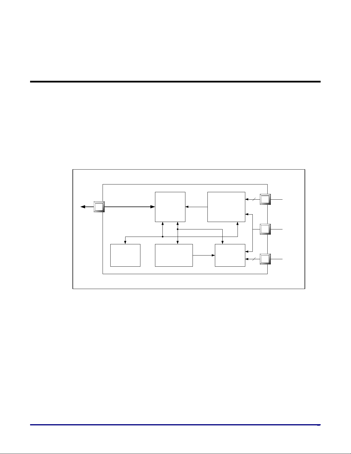
General Description and Architecture
JTAP Interface
Read-
Write
Control
Trigger
Detector
BRAM
Read/Write
Address
Counters
Registers
40
80-320
Trigger-Ch
User Clk
Monitor-Ch
The Snapshot macro samples user-signals in real time, and sends the captured data back
through the JTAG interface. The implementation supports the following features:
- Capture up to 144-bit wide data.
- Capture always 1024 samples of data at the user clock frequency
- Supports up to three separate 36-bit trigger conditions, each capable of operating on
any user signal. Each trigger condition supports “don’t care” feature (masking)
- All captured data will be read back serially with respect to TCK
Figure 2 shows the Snapshot architecture:
UG016, September 22, 2014
Figure 2: Snapshot Block Diagram
The blocks comprising the Snapshot module are described in more detail in the following
sections.
JTAP Interface
The JTAG based tap controller, or JTAP, is a module auto-generated when Snapshot is used
in the design. It provides handshaking and connectivity between the Snapshot core in the
user logic and the JTAG interface.
5
Page 6
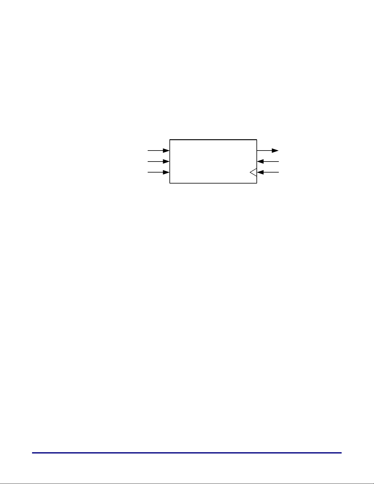
Trigger Detector
sel_in
pattern_in [35:0]
channel_in [35:0]
don’t_care [35:0]
usr_clk
match_out
Trigger Detector
As illustrated in Figure 3, the Trigger Detector receives one 36-bit each from the trigger
pattern (pattern_in), don’t care sequence (mask), and input data (channel_in). For every
channel_in sample, this block evaluates a corresponding match signal, called match_out. If
the corresponding mask bit is set high, match_out is asserted; otherwise, match_out remains
low, and is only asserted if the corresponding channel_in bit matches the pattern_in bit.
There is a sel_in pin which comes from a JTAG register for selecting between match_out
getting ORed or ANDed. If sel_in pin is asserted high match_out is ANDed or if sel_in pin is
asserted low match_out is ORed.
Figure 3: Trigger Detector
Note: The 36bit trigger signals must always be the lowest 36 bits of the monitor signals
Read-Write Control Logic
The read-write control logic is essentially a set of state machines to interface with the
counters, the BRAM and the trigger detect circuitry to generate the appropriate signals for
proper storage of user data in the BRAM and for retrieval of this data to be displayed for the
user. It is the main interface between the JTAG circuitry in the rest of the modules in the
Snapshot macro and operates in the same domain as the user clock.
Counters and Registers
The read/write address counters are controlled through the read-write control logic, and
essentially ensure that captured data is appropriately written to and read from the BRAM.
There are also additional registers to monitor triggering mechanisms as well as for
implementation of the read-write control logic.
6 UG016, September 22, 2014
BRAM
The BRAM is the memory module used for storage of the captured data. It is a 80Kbit fully
featured true dual port (TDP) memory which acts as the buffering mechanism to supply the
captured data to the user through JTAG. More infotmation can be found on the BRAM in the
Speedster22iHD datasheet and the Speedster22iHD Macro Cell Library.
Page 7

Snapshot Interface
Pin Name
Type
Description
tck
Input
JTAG test clock
rstn
Input
JTAG test reset (active low)
tdi
Input
JTAG test data in
tms
Input
JTAG test mode select
tdo
Output
JTAG test data out
Monitor_ch
[MNTR_WIDTH-1:0]
trigger_ch [35:0]
Input
36-bit trigger channel data
usr_clk
Input
User clock (same as user design clock)
Reset output to reset user’s logic block if needed.
Otherwise, the user can leave this pin floating
Asserted when Snapshot logic starts observing the
when Snapshot logic is reset via the GUI.
Values output on this bus are set by the user via the
3rd trigger pattern value in the GUI.
Parameter
Defined Value
Default Value
{36,72, 108, 144}
sample size will always be 1024.
Field provided to the user to help distinguish
SnapShot logic instances in different devices
Add this many cycles of latency to the Arm
speeds
Below is the port list of the Snapshot macro:
Table 1: Pin Descriptio ns of Snapshot Macro
Input 36-144 bit tapped user logic data bus
Rstn_out* Output
Arm* Output
Stimuli* Output
*These outputs are in the “usr_clk” domain and can be used in the Design-Under-Test (DUT)
to create desired events to be observed.
monitor channels and trigger values. De-asserted
Table 2: Parameter Defitions
MNTR_WIDTH
DUTNAME
OUTPUTPIPELINING
User-defined based on how many signals need
to be monitored in Snapshot. The captured
and Stimuli outputs to enable fast usr_clk
144
"none_specified"
0
UG016, September 22, 2014
7
Page 8

Implementation
The ACX_SNAPSHOT macro is the top level module in the implementation of Snapshot. This
macro exists inside the Speedster Black-Box library file (for example: speedster_bb_synplify.v
for Synplify Pro users and speedster_bb_precision.v for Precision users) which must be
synthesized together with the user design (instantiation example shown below). User must
include the “speedster_bb*.v” file during synthesis while implementing the Snapshot macro.
Two clocks are present inside the Snapshot macro. These two clocks are
1. usr_clk: This clock is used for the user data in to the Snapshot macro
2. tck: This clock is used to read the data-out from Snapshot macro through the JTAG
tdo port. It is IEEE 1149.1 JTAG based TCK.
The usr_clk must match the desired clock frequency of the user’s design. Below is an
example how to implement the Snapshot macro inside the user’s design:
Example of Verilog Instantiation:
//////// Verilog Module for Top-Level Design Example with Snapshot Macro ///////
///////// as well as User’s Design block. This example will guide the user how //////
///////// to implement Snapshot macro with User’s Logic block. ////////////////////////////
module user_design_with_snap_shot (
input tck,
input trstn,
input tms,
input tdi,
output tdo,
input usr_clk
);
parameter MNTR_WIDTH = 72;
///// This above parameter should be varied (36, 72,108, 144) depending on user signals
///// to be monitored
wire [MNTR_WIDTH-1 :0] monitor_ch; /// Signals monitored in Snapshot
wire [35:0] trigger_ch; ///// Signals going to trigger-detector block to do pattern matching
wire rstn_out ; ///// Active low user reset signal.
wire Arm; ///// Indicates Snapshot activity.
wire [35:0] Stimuli; ///// User specified values for 3rd trigger pattern value
//////// Now Snapshot macro block instantiation ///////
ACX_SNAPSHOT #(.MNTR_WIDTH(MNTR_WIDTH))
snapshot_instance (
.tck(tck),
.tms(tms),
.trstn(trstn),
.tdi(tdi),
.tdo(tdo),
.usr_clk(usr_clk),
8 UG016, September 22, 2014
Page 9

.Monitor_ch(monitor_ch),
.trigger_ch(trigger_ch),
.rstn_out (rstn_out),
.Arm (Arm),
.Stimuli (Stimuli)
);
/////// NOTE: Parameter value sections for Snapshot macro //////
/////// Depend on Monitor Channel width //////
/////// Below is the Table showing how the RAM size parameter ////
/////// is impacted by the Monitor Channel width ///////////////////////
/***************************
RAM_SIZE Monitor-Channel-Width
36
72
108
144
***************************/
users_logic users_logic_block_instance ( .clk(usr_clk),
.rstn(rstn_out),
.data_out_from_block(monitor_ch),
.data_for_trigger(trigger_ch),
.snapshot_arm(Arm),
.stimuli(Stimuli)
);
endmodule
///////////// End of Sample Example ////////////////////////
Example of VHDL Instantiation:
--- VHDL entity for Top-Level Design Example with Snapshot Macro ---
--- as well as User’s Design block. This example will guide the user how ---
--- to implement Snapshot macro with User’s Logic block. --Library IEEE;
Use IEEE.std_logic_1164.all;
Use IEEE.std_logic_unsigned.all;
Use IEEE.numeric_bit.all;
entity user_design_with_snap_shot is
port ( tck : in std_logic;
trstn : in std_logic;
tms : in std_logic ;
tdi : in std_logic ;
tdo : out std_logic;
usr_clk : in std_logic );
end user_design_with_snap_shot;
architecture arch of user_design_with_snap_shot is
component ACX_SNAPSHOT is generic
( MNTR_WIDTH: natural := 144) ;
--- This above parameter should be varied (36, 72,108, 144) depending on user signal
--- to be monitored
port ( tck : in std_logic ;
UG016, September 22, 2014
9
Page 10

trstn : in std_logic ;
tms : in std_logic ;
tdi : in std_logic ;
tdo : out std_logic ;
usr_clk : in std_logic ;
Monitor_ch : in std_logic_vector (MNTR_WIDTH-1 downto 0);
trigger_ch : in std_logic_vector (35 downto 0) ;
rstn_out : out std_logic ;
Arm : in std_logic_vector (35 downto 0) ;
Stimuli : out std_logic) ;
end component ;
component users_logic is
port ( clk : in std_logic ;
rstn : in std_logic;
data_out_from_block : out std_logic_vector (MNTR_WIDTH-1 downto 0);
data_for_trigger : out std_logic_vector (35 downto 0);
snapshot_arm : out std_logic;
stimuli : out std_logic_vector (35 downto 0));
end component ;
---- SIGNAL DECLARATION --signal : monitor_ch_to_monitor : std_logic_vector (MNTR_WIDTH-1 downto 0) ;
signal : trigger_ch_to_trigger : std_logic_vector (35 downto 0) ;
--- THESE SIGNALS WILL GO TO TRIGGER-DETECTOR BLOCK TO DO ---- ----
--- PATTERN MATCHING ----signal : rstn : std_logic ;
signal : arm : std_logic ;
signal : stimuli : std_logic_vector (35 downto 0) ;
begin
---- MACRO INSTANTIATION --snapshot_instance : ACX_SNAPSHOT
generic map (MNTR_WIDTH => 144)
port map ( tck => tck,
trstn => trstn,
tms => tms,
tdi => tdi,
tdo => tdo,
usr_clk => usr_clk,
Monitor_ch => monitor_ch_to_monitor,
trigger_ch => trigger_ch_to_trigger,
rstn_out => rstn,
Arm => arm,
Stimuli => stimuli) ;
---- NOTE: GENERIC MNTR_WIDTH VALUE OF SNAPSHOT MACRO ---
---- DEPENDS ON MONITOR CHANNEL WIDTH. BELOW IS THE TABLE --- -
---- SHOWS HOW THE RAM SIZE GETS IMPLEMENT BY MONITOR CH WIDTH -
---------------------------------------------------------------
-- RAM_SIZE Monitor-Channel-Width
--- 0 36
--- 0 72
--- 1 108
--- 1 144
---------------------------------------------------------------
10 UG016, September 22, 2014
Page 11

users_logic_block_instance: users_logic
Snap_shot_core
36
Snapshot_top
User Logic
36
tck
trstn
tms
tdi
tdo
usr_clk
Monitor_ch
trigger_ch
36
Arm
Stimuli
rstn_out
port map ( clk => usr_clk,
rstn => rstn,
data_out_from_block => monitor_ch_to_monitor ,
data_for_trigger => trigger_ch_to_trigger,
snapshot_arm => arm,
stimuli => stimuli);
----- END VHDL EXAMPLE ---
After incorporating the Snapshot macro into the design, the user will be able to synthesize
the design with the Synplify-Pro or Precision synthesis tool. After synthesis, the generated
netlist can be imported into ACE (Achronix CAD Environment), to generate the FPGA
programming file.
Note: To implement the Snapshot macro, the user needs to include timing and placement
constraints via an SDC and PDC file. Below are the Snapshot-specific constraints:
UG016, September 22, 2014
Figure 4: Block diagram of Snapshot macro connection to user’s logic
11
Page 12

Clock constraints (SDC file):
###### CLOCK CONSTRAINTS INSIDE .SDC FILE #####
create_clock -period 10ns usr_clk
create_clock –period 40ns snapshot_instance.core_y_tck
##### THIS snapshot_instance.core_y_tck IS AN INTERNAL ######
##### TEST CLOCK GENERATED INSIDE THE SNAPSHOT-MACRO ####
##### BLOCK. IT IS MANDATORY FOR THE USER TO #######
##### CONSTRAINT THIS CLOCK PROPERLY; OTHERWISE #######
##### SNAPSHOT-MACRO WILL NOT WORK ON THE BOARD ########
set_false_path –from usr_clk –to snapshot_instance.core_y_tck
set_false_path –from snapshot_instance.core_y_tck –to usr_clk
NOTES:
1. In ACE there is a Tap-Controller (JTAP) macro embedded inside which meets the
IEEE1149.1 JTAG standard. All the JTAG specific signals get automatically assigned
in ACE during back-end procedure. So that user does not need to assign any
constraints for these JTAG signals.
12 UG016, September 22, 2014
Page 13

Snapshot GUI in ACE
The following procedures describe how to invoke the Snapshot view in ACE.
1. Open the ACE GUI tool as shown in Figure 5.
Figure 5: ACE Tool
After programming the Achronix FPGA successfully, user will be ready to use the “Snapshot
Debugger” tool. To go to the Snapshot Debugger tool, the user needs to click on the
“Snapshot Debugger” tab from the upper left side. Then the user will see the Snapshot
Debugger window as shown in Figure 6.
2. The following figure depicts the GUI of the Snapshot Debugger tool.
UG016, September 22, 2014
13
Page 14

Figure 6: Snapshot Debugger Tool view
a. Select the Download tab from the GUI
b. Specify the correct pod name in the “Specify Pod Name” box.
c. Match the “Monitor Channel Width” size (drop-down box) to the Monitor_ch size
that is connected to the snap_shot_core module inside the RTL.
d. Select either “Trigger1” or “Trigger 2” or “Trigger 3”, depending on how many
trigger conditions must be met before data is captured. For each of the trigger
conditions, enter the desired matching pattern and masking sequence (don’t cares)
e. Set the Frequency to match the usr_clk constraint set in the SDC file.
f. Snapshot is now ready to be triggered. Select the “Arm” button, and the Snapshot
debugging tool will begin to analyze the design, wait for the trigger conditions to be
matched, and display the captured results to the “Snapshot.log” file in the GUI or
VCD file in the waveform GUI.
In the Snapshot Debugger GUI, there are several options including “JTAG Scan Chain”,
“Trigger”, “Monitor Channel Width”, “Pre_store”, “Select Using AND”, and “Select Using
OR”, “Arm”, and “Cancel” to specify or customize the data logging mechanism. These
options are described below.
14 UG016, September 22, 2014
Page 15

JTAG Scan Chain: This option has several sub-options.
Target Device Offset
in Scan Chain
1
0 0 46
2
1
23
23
3
2
46
0
a. IR Bits Before Device: This option sets the number of instruction register bits before
the target FPGA device. Default value is ‘0’. (e.g. There are 23 IR-Bits in
Speedster/RadRunner. If the user has multiple Achronix FPGA devices being programmed on
the board through the JTAG Scan Chain, the user needs to specify this bit in the box. At the
end of this section this example will give an idea on how to set these values.)
b. IR Bits After Device: This sets the number of instruction register bits after the target
FPGA device. Default setting is ‘0’.
c. Target Device Offset in Scan Chain: It sets the cardinal number of the device in the
scan chain. Default is ‘0’.
Example: If the user has three Achronix FPGA devices already programmed via the JTAG
Scan Chain on the system, the user needs to implement the following in the Snapshot GUI:
Table 3: JTAG Scan Chain Example Implementation on the Snapshot GUI
Device
Trigger: The radio buttons to the left of the trigger groups allow the user to select the use of
1, 2, or 3 sequential triggers. If the radio button to the left of Trigger 1 is selected, Trigger 2,
and Trigger 3 are ignored. If the radio button to the left of Trigger 2 is selected, Trigger 3 is
ignored and Snapshot Debugger tool will trigger when Trigger 1 is matched, followed by a
match on Trigger 2. If the radio button next to Trigger 3 is selected, then Snapshot will trigger
after a match on Trigger 1, followed by Trigger2, followed by Trigger3.
a. Pattern: This trigger pattern specifies the 36-bit pattern of ‘1’s and ‘0’s to match on.
Each bit corresponds to one of the signals attached to monitor channels 0-35. The LSB
of this pattern bus connects to the monitor channel LSB, which is bit 0, and the MSB
of the pattern data will be connected to monitor channel MSB, which is bit 35. The
trigger pattern can be set either in HEX, or in BINARY.
b. Don’t Care: The Don’t Care bits specify which bits out of the trigger pattern are
ignored during a compare. If Don’t Care bit 3 is set to a ‘1’, then the signal attached to
monitor channel 3 will be ignored during trigger pattern compare. The Don’t Care
pattern can be set either in HEX, or in BINARY.
IR Bits Before Device IR Bits After Device
UG016, September 22, 2014
Monitor Channel Width: The Snapshot macro is parameterizable to channel widths of 72
and144 channels. The user must set the Monitor Channel Width to the value that corresponds
with the parameterized Snapshot RTL instantiation. Note that channels 0-71 are always
connected to the trigger mechanism. Once you have selected the Monitor Channel Width, the
signal names for each channel may be configured in the Monitor Channels table.
Pre-Store: This is an option which the user can set during the “Arm”ing of Snapshot. There
are four selections for this (0%, 25%, 50%, and 75%). When set to 0%, Snapshot macro begins
collecting samples once the trigger event is met. If set to 25%, 25% of the trace buffer depth is
filled with pre-trigger samples and the rest are post trigger samples. Similarly, when 50% is
selected, 50% of the trace buffer depth is filled with pre-trigger samples and the rest are post
trigger samples. 75% setting directs the Snapshot macro to collect 75% of the trace buffer
depth with pre-trigger samples and the rest are port trigger samples. Default setting is 0%.
15
Page 16

Select Using AND: This option is used to set the trigger condition on the 72-bit bus to be
captured.
Select Using OR: This option is used to set the trigger condition on the particular bits of the
72-bit bus to be captured.
Arm: This is to send the configuration file to the Snapshot Debugger tool, wait for the trigger
condition to be met, retrieve the trace buffer contents, and output a VCD file as well as a LOG
file.
Cancel: This option is to direct the tool to stop the operation. (Limitation: This option
requires power cycling the Bit-porter Pod before continuing).
3. When a trigger event occurs after a proper “Arm”, the Snapshot Debugger will display
the waveform of the monitored signals (Monitor_ch in RTL). shows an example
waveform.
Figure 7: Snapshot Debugger waveform view
To ascertain the signal’s identities, the user must match up the signal# to the Monitor_ch
assignment in the RTL.
In future releases of ACE, the signal names in the waveform will be automatically populated
with the names from the netlist, making the waveform signal names less cryptic.
16 UG016, September 22, 2014
Page 17

4. Save Snapshot Configuration file and Load Snapshot Configuration file: The Snapshot
Icon
Action
IR Bits Before Device
Saves the current settings of the Snapshot view to a text file
GUI inferred settings will be saved in this file.
The Snapshot debugger loads a previously saved
configuration file.
Debugger tool has options to save the Snapshot configuration file and to load the
previously saved configuration file. Below is the table which depicts the functionality of
these two options:
Table 4: Snapshot view of toolbar options to save and load configuration files
Save configuration
(default filename is *.Snapshot). User can also give the
specific file name for the configuration file to be saved. All
Load configuration
5. Collecting Samples of the design: In the Snapshot Debugger tool there are two ways to
collect the samples: The first is in the LOG-File and the other is in the Waveform File.
“Log File” sets the file name for the log file from “Arm” of the Snapshot Debugger Tool.
The Browse button allows for the selection of a location different from the default
(./Snapshot.log). If an error occurs during setup or while reading back the sample
information, the Snapshot log file will contain the error messages. The user can visit these
error messages and fix the appropriate setting to “Arm” Snapshot Debugger Tool again.
“Waveform File” sets the file name for storing downloaded samples’ waveform
information from the Snapshot Debugger in VCD format. The Browse button allows for
the selection of a location different from the default (./Snapshot.vcd). The significance of
this VCD file is that the user can load this VCD file into any 3rd party simulation tool and
view the signals of the user design.
UG016, September 22, 2014
17
Page 18

Revision History
4/05/2013
1.0
Initial Achronix release.
4/17/2013
1.1
Updated module name to ACX_SNAPSHOT
9/22/14
1.2
Modified to 144 bit sample and 36 bit trigger
The following table shows the revision history for this document.
Date Version Revisions
18 UG016, September 22, 2014
 Loading...