

Page 1

1
Speedster22i Pin Connections and
Power Supply Sequencing
User Guide
UG042 – August 19, 2014
UG042, August 19, 2014
Page 2

Copyright Info
Copyright © 2014 Achronix Semiconductor Corporation. All rights reserved. Achronix is a trademark and Speedster is a
registered trademark of Achronix Semiconductor Corporation. All other trademarks are the property of their prospective owners.
All specifications subject to change without notice.
NOTICE of DISCLAIMER: The information given in this document is believed to be accurate and reliable. However, Achronix
Semiconductor Corporation does not give any representations or warranties as to the completeness or accuracy of such
information and shall have no liability for the use of the information contained herein. Achronix Semiconductor Corporation
reserves the right to make changes to this document and the information contained herein at any time and without notice. All
Achronix trademarks, registered trademarks, and disclaimers are listed at http://www.achronix.com and use of this document
and the Information contained therein is subject to such terms.
2 UG042, August 19, 2014
Page 3
3
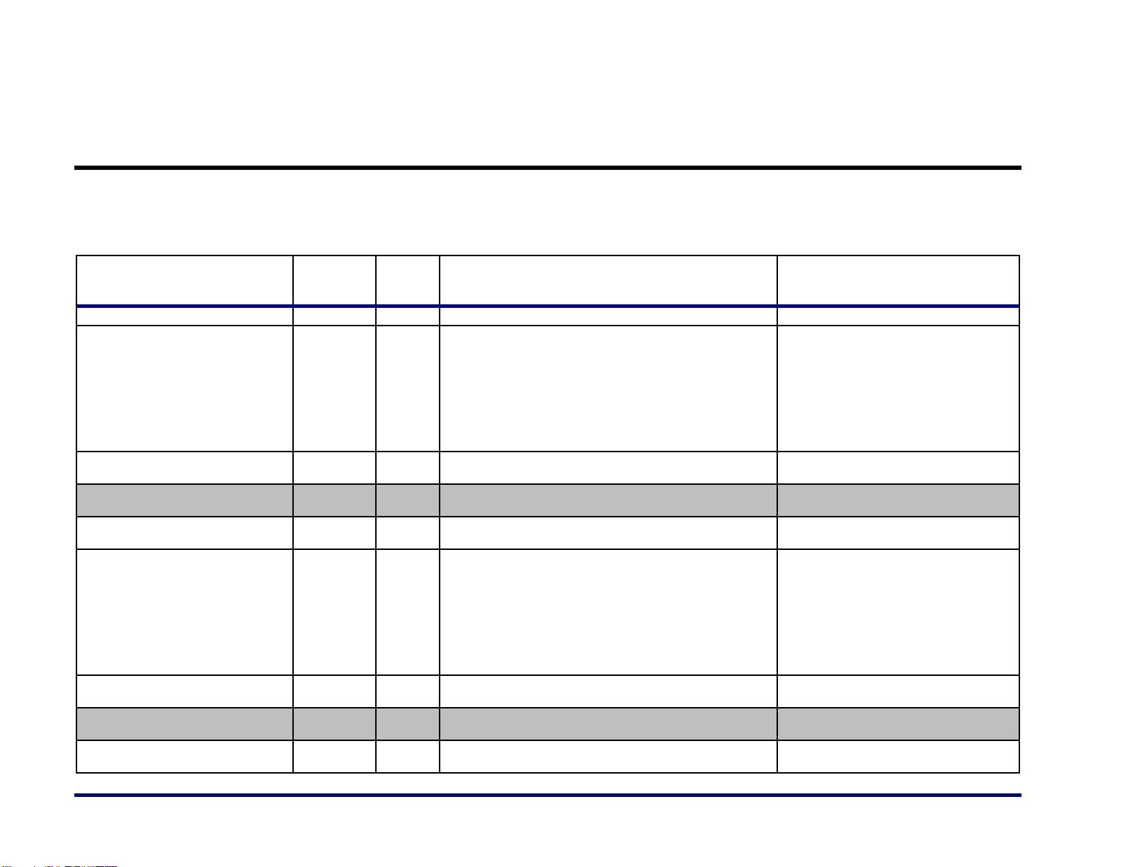
Pin Connection Guidelines
Pin Name
Pin
Group
Type
Description
Connection Guidelines
12.75 Gbps SerDes (64 lanes)
PAD_TE_I_BCK_REF_P/M_LNUM[31:0]
N12P75G
Clock
The 12.75 Gbps SerDes reference clock supplied from either a
single-ended or differential external source. There is 1
differential pair for each of 2, 12.75Gbps lane.
Connect these clocks for all SerDes lanes
used in the interface. Unused clocks should
be tied to their own individual GND via a
50Ω +/- 1% termination resistor.
Note: For PCIe Gen3 operation when using
the hard PCIe controller, reference clocks
for all 8 SerDes lanes need to be connected
regardless of the data width implemented.
PAD_TE_I_BA_RX_P/M_LNUM[31:0]
N12P75G
Input
Receive differential inputs to the 12.75 Gbps SerDes. One pair
for each lane.
Connect all unused receive pins directly to
GND via a 50Ω +/- 1% termination resistor.
PAD_TE_O_BA_APROBE_LNUM[31:0]
N12P75G
Output
The 12.75 Gbps SerDes Analog DC test pad used internally for
debug and testing, one for each lane.
Leave unconnected.
PAD_TE_O_BA_TX_P/M_LNUM[31:0]
N12P75G
Output
Transmit differential outputs from the 12.75 Gbps SerDes.
There is one differential pair per each 12.75Gbps lane.
These pins should be AC coupled. Leave all
unused transmit pins unconnected.
PAD_BE_I_BCK_REF_P/M_LNUM[31:0]
S12P75G
Clock
The 12.75 Gbps SerDes reference clock supplied from either a
single-ended or differential external source. There is 1
differential pair for each of 2, 12.75Gbps lane.
Connect these clocks for all SerDes lanes
used in the interface. Unused clocks should
be tied to their own individual GND via a
50Ω +/- 1% termination resistor.
Note: For PCIe Gen3 operation when using
the hard PCIe controller, reference clocks
for all 8 SerDes lanes need to be connected
regardless of the data width implemented.
PAD_BE_I_BA_RX_P/M_LNUM[31:0]
S12P75G
Input
Receive differential inputs to the 12.75 Gbps SerDes. One pair
for each lane.
Connect all unused receive pins directly to
GND via a 50Ω +/- 1% termination resistor.
PAD_BE_O_BA_APROBE_LNUM[31:0]
S12P75G
Output
The 12.75 Gbps SerDes Analog DC test pad used for ATE and
bench testing, one for each lane
Leave unconnected.
PAD_BE_O_BA_TX_P/M_LNUM[31:0]
S12P75G
Output
Transmit differential outputs from the 12.75 Gbps SerDes.
There is one differential pair per each 12.75Gbps lane.
These pins should be AC coupled. Leave all
unused transmit pins unconnected.
Please see the table below on guidelines for connecting all IOs on the Speedster22i HD FPGAs. For completeness, debug I/Os that
have no user functionality have also been included and are indicated by a grey background.
UG042, August 19, 2014
Page 4
IEEE1149.1 JTAG Interface
Do not leave JTAG I/Os unconnected. The
JTAG interface should be brought out to a
JTAG header on the board.
TMS
JTAG
Input
Test Mode Select (TMS) input controlling the test access port
(TAP) controller state machine transitions. This input is
captured on the rising edge of the test logic clock (TCK).
This dedicated pin is equipped with an
internal pull-up resistor to place the test
logic in the Test-Logic-Reset state. Connect
this pin using a 10-kΩ +/- 5% pull-up
resistor to VDDO_JCFG (1.8V).
TCK
JTAG
Input
Dedicated test clock used to advance the TAP controller and
clock in data on TDI input and out on TDO output. The
maximum frequency for TCK is 100 MHz.
Connect this pin using a 1-kΩ +/- 1% pulldown resistor to GND.
TDI
JTAG
Input
Serial input for instruction and test data. Data is captured on
the rising edge of the test logic clock.
Dedicated pin with an internal pull-up
resistor. Connect this pin using a 10-kΩ +/5% pull-up resistor to VDDO_JCFG (1.8V).
TRSTN
JTAG
Input
Active-low reset input used to initialize the TAP controller.
Dedicated pin and an optional port on
some devices. Connect this pin using a 4.7kΩ +/- 5% pull-down resistor to GND.
TDO
JTAG
Output
Serial output for data from the test logic. TDO is set to an
inactive drive state (high impedance) when data scanning is
not in progress. TDO drives out valid data on the falling edge
of the TCK input.
Use a 10-kΩ +/- 5% pull-up resistor to
VDDO_JCFG (1.8V) to minimize leakage in
the TDI input buffer of interfacing devices.
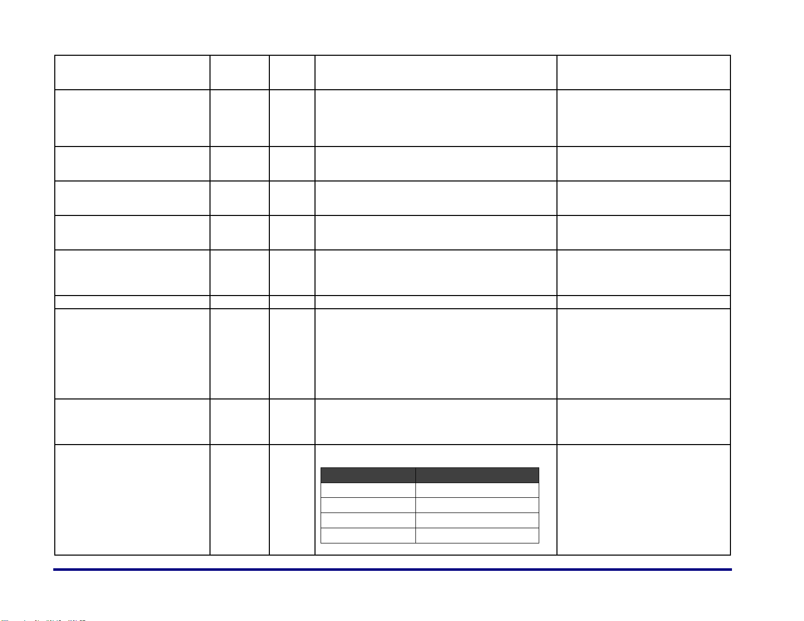
Configuration Interface
CONFIG_STATUS
CFG
Open
drain
output
Signal from open-drain output pulled low by FCU until the
configuration memory is successfully cleared. After this, I/O is
tri-stated and the external pull-up should pull this signal high.
It is recommended to connect this signal to
an LED as an indicator on the board. In this
case, use an external 10-kΩ +/- 5% pull-up
resistor to 3.3V and drive a 1-kΩ resistor to
the input of a FET to turn on the LED. If LED
usage is not desired, this signal can be
pulled-up to 1.8V (VDDO_JCFG / PA_VDD2)
using the same 10-kΩ pull-up resistor.
CONFIG_RSTN
CFG
Input
Asynchronous active-low reset input clearing the
configuration memory in the device and the logic in the FPGA
configuration unit (FCU).
Connect directly to the configuration
controller and pull up to 1.8V (VDDO_JCFG
/ PA_VDD2) through a 10-kΩ +/- 5%
resistor.
CONFIG_MODESEL[2:0]
CFG
Input
Configuration mode selection inputs to define the FPGA
configuration unit (FCU) mode of operation.
Configuration Mode
CONFIG_MODESEL[2:0]
Serial x1 Flash
001
Serial x4 Flash
010
CPU
100
JTAG
Always active
Do not leave these pins unconnected. They
should be connected to configurable inputs
like DIP switches to toggle between modes
of operation for debug. If this is not
possible or desired, based on the config
scheme, these pins should be tied to 1.8V
(VDDO_JCFG / PA_VDD2) or GND.
4 UG042, August 19, 2014
Page 5

5
PROGRAM_ENABLE[1:0]
CFG
Input
Pin enabling the programming of the eFuse for the AES
encryption keys, which is done in the manufacturing and
testing of the devices. These input pins will not be usable by
customers.
Tie to GND.
CONFIG_DONE
CFG
Input
with
open-
drain or
active
output
Pin pulled low by FCU prior to the completion of device
configuration. After the device successfully completes
configuration, this pin is either tri-stated or can optionally be
driven high. The default behavior is open-drain, tri-stating the
pin when the device is properly configured. If a device
configuration error occurs, the CONFIG_DONE output for the
device remains in low. The device does not enter the
functional mode until this pin is high. Holding this pin low on
the board can be used as a method to synchronize the startup of multiple devices.
In the default mode of operation, it is
recommended that this signal be
connected to an LED as an indicator on the
board. In this case, use an external 10-kΩ
+/- 5% pull-up resistor to 3.3V and drive a
1-kΩ resistor to the input of a FET to turn
on the LED. If LED usage is not desired, this
signal can be pulled-up to 1.8V
(VDDO_JCFG / PA_VDD2) instead using the
same 10-kΩ pull-up resistor.
CONFIG_CLKSEL
CFG
Input
Pin controlling whether the FCU clock is sourced from the TCK
input or the CPU_CLK input.
CONFIG_SYS_
CLK_BYPASS
CONFIG_
CLKSEL
CONFIG_MODESEL
[2:0]
FCU CLK
0 0 001, 010
On-chip
oscillator
1 0 001, 010
CPU_CLK
0/1 0 100
CPU_CLK
0
1
000, 001, 010, 100
TCK
Do not leave this pin unconnected. It
should be connected to a configurable
input like a DIP switch to toggle between
modes of operation for debug. If this is not
possible or desired, tie this off to 1.8V
(VDDO_JCFG / PA_VDD2) or GND based on
the desired clock for the configuration
mode.
HOLDN
CFG
Input /
Output
In the SPI mode of operation, the hold signal output for SPI
flash devices. In CPU mode, this bit is the bidirectional data
bit 5, DQ[5].
Connect directly to the configuration
controller. Do not leave this pin
unconnected.
CPU_CLK
CFG
Clock
Maximum 25Mhz. Used as FCU clock under CONFIG_CLKSEL
control.
If the CPU_CLK is not used to source the
FCU clock, then pin should be tied to GND.
BYPASS_CLR_MEM
CFG
Input
Input to enable bypassing of the configuration memory
clearing before device configuration.
Do not leave this pin unconnected. It
should be connected to a configurable
input like a DIP switch, or even dynamically
controlled through the configuration
controller. This will enable toggling
between modes of operation for debug and
may help with re-configuration time
optimization. If this is not possible or
desired, this pin should be tied to GND.
SCK
CFG
Output
Serial flash clock output. Clock can be sourced from either
CPU_CLK (user driven) or on-chip oscillator (~10MHz).
For SPI Mode: Connect directly to the flash
device(s).
For CPU Mode: Leave unconnected.
SDI
CFG
Input /
Output
In the SPI modes of operation, the serial data output pins for
command and programming data to the flash memory. These
Connect directly to the configuration
controller. Do not leave this pin
UG042, August 19, 2014
Page 6

command and programming commands are sent via control
registers writes done via the IEEE 1149.1 JTAG interface. In
the CPU mode, this pin is the bidirectional data bit 0, DQ[0]
unconnected.
CSN[3:0]
CFG
Input /
Output
In SPI Mode: The CSN[3:0] pins are active-low chip select
outputs. In the programming mode, individual serial flash
devices are mapped to a linear addressing space. In the SPI x1
configuration mode only the CSN[0] output is used.
In CPU Mode: CSN[3] is the bidirectional data bit 6, DQ[6].
CSN[2] is the bidirectional data bit 7, DQ[7]. CSN[1] is not
used. CSN[0] is an active-low chip select input.
For SPI Mode: If SPIx1 is used, leave
CSN[3:1] unconnected. In SPIx4, connect all
four to the individual serial flash devices.
For CPU Mode: Connect CSN[3], CSN[2] and
CSN[0] directly to the configuration
controller. Tie CSN[1] to GND.
SD[3:0]
CFG
Input
Input pins providing data input from the flash device(s). In SPI
x4 configuration mode, all 4 SD inputs are utilized. When in
SPI x1 mode, only the SD[0] input is used to input the
configuration data. In the CPU mode, these bits serve as the
bidirectional data bits 1 through 4 (SD3=DQ1, SD2=DQ2,
SD1=DQ3, SD0=DQ4)
Connect directly to the configuration
controller. Do not leave these pins
unconnected.
CONFIG_SYS_CLK_BYPASS
CFG
Input
Pin statically enabling the bypass of the internal SYS_CLK. The
default clock for the FPGA configuration unit (FCU) is named
SYS_CLK. An on-chip ring oscillator (~10MHz) is the source for
SYS_CLK. For debug purposes this clock can be bypassed and
an external clock supplied.
CONFIG_SYS_
CLK_BYPASS
CONFIG_
CLKSEL
CONFIG_MODESEL
[2:0]
FCU CLK
0 0 001, 010
On-chip
oscillator
1 0 001, 010
CPU_CLK
0/1 0 100
CPU_CLK
0
1
000, 001, 010, 100
TCK
Do not leave this pin unconnected. It
should be connected to a configurable
input like a DIP switch to toggle between
modes of operation for debug. If this is not
possible or desired, tie this off to 1.8V
(VDDO_JCFG / PA_VDD2) or GND based on
the desired clock for the configuration
mode.
START_CFG_STARTUP
CFG
Input
Used to restart the configuration startup state machine after
the startup is already complete. This option is used if any
errors are encountered in the configuration memory from
ECC. NOT Available for HD1000.
For the HD1000 tie this pin to GND. For
other devices, connect this pin directly to
the configuration controller.
STAP_SEL
CFG
Input
When asserted high, this allows the JTAG interface pins to be
directly connected to the JTAG controller in Serdes PMA
blocks allowing SerDes configuration, debug and performance
monitoring directly from the JTAG interface. For bitstream
download and chip debug using the JTAG interface, this pin
must be held low. For SerDes PMA debug only mode, this pin
must be held high.
Do not leave this pin unconnected. It
should be connected to a configurable
input like a DIP switch to toggle between
modes of operation for debug.
READ_STATE_ERR
CFG
Output
Debug output signal in fabric testing.
Leave unconnected.
CONFIG_SCRUB_MULTIPLE_ERR
CFG
Output
Indicates the presence of multiple errors when the SCRUB
For the HD1000, leave unconnected. For
6 UG042, August 19, 2014
Page 7

7
feature is used. NOT Available for HD1000.
other devices, connect directly to
observation point for error.
CONFIG_SCRUBBING_ENABLE
CFG
Input
Enables SCRUB feature for SEU mitigation in the configuration
memory. NOT Available for HD1000.
For the HD1000 tie this pin to GND. For
other devices, connect this pin directly to
the configuration controller.
CONFIG_SCRUB_SINGLE_ERR
CFG
Output
Indicates the presence of a single error when the SCRUB
feature is used. NOT Available for HD1000.
For the HD1000, leave unconnected. For
other devices, connect directly to
observation point for error.
General Purpose I/O Interface
RCOMP_TERM_B
[00,01,02,10,11,12,20,21,22,
30, 31,32,40,41,42,50,51,52]
BWN, BWC,
BWS, BES,
BEC, BEN
Input
Termination resistor input for dynamic drive compensation
for PVT and aging.
Terminate to GND through a changeable /
swappable resistor that will provide the
correct termination. Currently a 200Ω +/1% resistor is being used internally.
RCOMP_DRV_B
[00,01,02,10,11,12,20,21,22,
30, 31,32,40,41,42,50,51,52]
BWN, BWC,
BWS, BES,
BEC, BEN
Input
Drive resistor input for dynamic drive compensation for PVT
and aging.
Terminate to GND through a changeable /
swappable resistor that will provide the
correct drive strength. Currently a 25Ω +/1% resistor is being used internally.
PAD_[WS/WC/WN/ES/EC/EN]_BYTEIO
[12:0]DQ[9:0]
BWN, BWC,
BWS, BES,
BEC, BEN
Input /
Output
A group of 13 byte lanes. Each byte lane has 12 bits; 10 of
these 12 bits are used as data for memory interface
applications. Alternatively, these I/Os could be set for Single
Ended, Differential, LVCMOS, *STL and LVDS modes.
Unused I/Os can be left unconnected.
PAD_[WS/WC/WN/ES/EC/EN]_BYTEIO
[12:0]DQS
BWN, BWC,
BWS, BES,
BEC, BEN
Input /
Output
A group of 13 byte lanes. Each byte lane has 12 bits; the 11th
bit carries a synchronous strobe signal (positive polarity
differential clock) for referencing DQ[9:0] in each of the byte
lanes. Alternatively, these I/Os could be set for Single Ended,
Differential, LVCMOS, *STL and LVDS modes.
Unused I/Os can be left unconnected.
PAD_[WS/WC/WN/ES/EC/EN]_BYTEIO
[12:0]DQSN
BWN, BWC,
BWS, BES,
BEC, BEN
Input /
Output
A group of 13 byte lanes. Each byte lane has 12 bits; the 12th
bit carries a synchronous strobe signal (negative polarity
differential clock) for referencing DQ[9:0] in each of the byte
lanes. Alternatively, these I/Os could be set for Single Ended,
Differential, LVCMOS, *STL and LVDS modes.
Unused I/Os can be left unconnected.
Clock I/O Interface
RCOMP_TERM_CLK_BANK_[NW/SW/S
E/NE]
CB0, CB1,
CB2, CB3
Input
Termination resistor input for dynamic drive compensation
for PVT and aging.
Terminate to GND through a changeable /
swappable resistor that will provide the
correct termination. Currently a 200Ω +/1% resistor is being used internally.
RCOMP_DRV_CLK_BANK_[NW/SW/SE
/NE]
CB0, CB1,
CB2, CB3
Input
Drive resistor input for dynamic drive compensation for PVT
and aging.
Terminate to GND through a changeable /
swappable resistor that will provide the
correct drive strength. Currently a 25Ω +/1% resistor is being used internally.
PAD[5:0]_CLK_BANK_[NW/SW/SE/NE]
CB0, CB1,
CB2, CB3
Input /
Output
A group of six clock buffers that can be used either as three
differential I/Os or six single‐ended I/Os. If these I/Os are not
used as clock buffers, they can be used as generic inputs or
outputs.
Unused I/Os can be left unconnected.
UG042, August 19, 2014
Page 8

8 UG042, August 19, 2014
Miscellaneous
CORE_TESTIN1
DBG
Output
Debug interface used for testing the fabric
Leave unconnected.
EDM
DBG
Output
For factory use / test purposes
Leave unconnected.
TEMP_DIODE_P/N
TEMP
Input
Die temperature monitoring diode connections (P and N).
If temperature monitoring feature is not
used, leave unconnected. Otherwise
connect directly to a temperature sensor.
EFUSE_PROG
EFUSE
Output
HD1000's EFuse erase / program sequencer controls this
signal. This signal should not be touched by user.
Leave unconnected.
Power
PA_VDD1
N12P75G
Power
SerDes Analog Low Power Supply
0.95V analog power supply for the SerDes.
Connect these pins to a linear or low noise
switching power supply.
PA_VDD2
N12P75G
Power
SerDes Analog High Power Supply
Connect all 1.8V PA_VDD2 pins to a linear
or low noise switching power supply. Highly
sensitive SerDes analog power supply.
PA_VREG_CMN
N12P75G
Power
SerDes Regulator Power Supply
0.95V power supply for the SerDes
regulator. Connect to PA_VDD1 through
ferrite bead.
PA_VREG_RX
N12P75G
Power
SerDes Regulator Power Supply
0.95V power supply for the SerDes
regulator. Connect to PA_VDD1 through
ferrite bead.
PA_VREG_SYNTHX
N12P75G
Power
SerDes Regulator Power Supply
0.95V power supply for the SerDes
regulator. Connect to PA_VDD1 through
ferrite bead.
PAD_TE_I_A_RXTERMV_LNUM[31:0]
N12P75G
Power
Receiver Termination Voltage Pad input
Use a 1nF bypass cap and terminate to
GND.
PA_VDD1
S12P75G
Power
SerDes Analog Low Power Supply
0.95V analog power supply for the SerDes.
Connect these pins to a linear or low noise
switching power supply.
PA_VDD2
S12P75G
Power
SerDes Analog High Power Supply
Connect all 1.8V PA_VDD2 pins to a linear
or low noise switching power supply. Highly
sensitive SerDes analog power supply.
PA_VREG_CMN
S12P75G
Power
SerDes Regulator Power Supply
0.95V power supply for the SerDes
regulator. Connect to PA_VDD1 through
ferrite bead.
PA_VREG_RX
S12P75G
Power
SerDes Regulator Power Supply
0.95V power supply for the SerDes
regulator. Connect to PA_VDD1 through
ferrite bead.
PA_VREG_SYNTHX
S12P75G
Power
SerDes Regulator Power Supply
0.95V power supply for the SerDes
regulator. Connect to PA_VDD1 through
ferrite bead.
PAD_BE_I_A_RXTERMV_LNUM[31:0]
S12P75G
Power
Receiver Termination Voltage Pad input
Use a 1nF bypass cap and terminate to
GND.
Page 9

9
AVDD_PLL_[SE, SW, NE, NW][3:0]
PLL
Power
Analog power supply for the PLLs feeding the FPGA core
fabric.
Connect all 1.7V AVDD_PLL pins to a linear
or low noise switching power supply. This is
a highly sensitive PLL analog power supply.
VDDO_JCFG
CFG
Power
Supply voltage powering the I/O buffers for the IEEE 1149.1
JTAG interface. The value selected determine the output VOH
level on TDO and set the input threshold VIL and VIH values
appropriately. (TAP) controller state machine transitions. This
input is captured on the rising edge of the test logic clock
(TCK). This dedicated pin is equipped with a pull-up resistor to
place the test logic in the Test-Logic-Reset state
Connect these pins to a 1.8V power supply.
This supply can be shared with the 1.8V
analog SerDes power supply (PA_VDD2).
Noise should not be a concern, since the
JTAG I/O buffers and SerDes will generally
not operate the same time. The one
exception is during in-system debug with
Snapshot, which should still be fine.
However, it would be preferable to have
this power supply be shared with a 1.8V
VDDO_B[xx] I/O power supply if 1.8V I/Os
are used in the design.
VDDL
CVDD
Power
Power Supply for FPGA fabric core logic
VDDL is the 1.0V core supply. Connect all
VDDL pins to a low noise switching
regulator. While VDDL is one of many 1.0V
supplies, it is recommended that a separate
regulator be used to ensure noise isolation
and for prevention of current spikes prior
to clearing of the configuration memory.
Refer to the supply power up/down
requirements below for further
information.
VCC
SVDD
Power
Digital Power Supply for FPGA circuitry in the I/O ring,
including the Hard IP.
Connect VCC to a 1.0V linear regulator. This
supply can be shared with VDD_CFG and
VDD_BRAM.
VCCRAM_EFUSE[3:1]
EFUSE
Power
Efuse Power Supply normal / read operations
Tie this to the 1.0V supply powering
VDDA_NOM_E/W
VCCFHV_EFUSE[3:1]
FFUSE
Power
Efuse Power Supply for Fuse Program / Erase operations
If the application requires fuse blowing (eg.
programming encryption fuses for design
security), this supply needs to be tied to a
regulator capable of providing output
voltages in the 1.0V – 2.2V range. For these
cases, this supply cannot be shared with
any other supply. If fuse blowing is not
needed, this supply can be tied to the 1.0V
regulator powering VDDA_NOM_E/W and
VCCRAM_EFUSE[3:1].
VDDA_NOM_E
EVDDA
Power
Analog Power Supply for FPGA circuitry in the I/O ring.
Connect VDDA_NOM_E to a 1.0V linear
regulator. The only 1.0V supplies that can
be shared with this supply are the eFuse
power supplies.
VDD_CFG
CFG
Power
Supply voltage for the configuration memory SRAM cells in
Connect VDD_CFG to a 1.0V linear
UG042, August 19, 2014
Page 10

the FPGA fabric.
regulator. This supply can be shared with
VCC and VDD_BRAM.
VDD_CFGWL
CFG
Power
Power Supply for the wordlines of the configuration memory
SRAM cells in the FPGA fabric.
For configuration memory readback
capability (primarily for debug purposes),
this supply would need to be set to 0.9V
using a separate regulator. If this capability
is not needed or desired, this supply can be
more simply set to 1.0V and shared with
VDD_CFG, VCC and VDD_BRAM.
VDDA_NOM_W
WVDDA
Power
Analog Power Supply for FPGA circuitry in the I/O ring.
Connect VDDA_NOM_W to a 1.0V linear
regulator. The only 1.0V supplies that can
be shared with this supply are the eFuse
power supplies.
VDD_BRAM
VDD_BRAM
Power
Power Supply for Block RAMS in Fabric.
Connect VDD_BRAM to a 1.0V linear
regulator. This supply can be shared with
VCC and VDD_CFG.
VREF_B[00,01,02,10,11,12,20,21,22,
30, 31,32,40,41,42,50,51,52]
VDD_BANK
Power
Analog input; Voltage Bias reference. Half of corresponding
bank / cluster voltage level.
Connect to a biasing circuit like a
termination regulator with a reference
based on the corresponding I/O cluster's
power supply.
VDDO_B[00,01,02,10,11,12,20,21,22,
30, 31,32,40,41,42,50,51,52]
VDD_BANK
Power
Bank I/O supply voltage. An I/O bank is defined as a group of
byte-lanes that have a common power ball eg. 00. 3 I/O banks
make up an I/O cluster eg. 00, 01, 02. x0 and x1 I/O banks
have 4 byte lanes each and x2 I/O banks have 5 byte lanes to
give a total of 13 byte-lanes or (13x12) 156 I/O pins.
Note: Even though each I/O bank has a separate power ball,
all 3 I/O banks in the I/O cluster are required to be set to the
same voltage due to internal power rail sharing.
The I/O supply voltage can be set to 1.2V,
1.5V or 1.8V. The I/O standard can be
configured at a single I/O pin granularity,
but because all I/Os in the same I/O cluster
share a common supply, the standards
need to be voltage compatible.
VREF_CLK_BANK_[SE, SW, NE, NW]
VDD_BANK
Power
Analog input; Voltage Bias reference for clock banks. Half of
corresponding bank voltage level.
Connect to a biasing circuit like a
termination regulator with a reference
based on the corresponding clock bank's
power supply.
VDDO_CB[SE, SW, NE, NW]
VDD_BANK
Power
Clock bank I/O supply voltage
The I/O supply voltage can be set to 1.2V,
1.5V or 1.8V. The I/O standard can be
configured at clock bank corner granularity.
VSS
VSS
Power
Ground
All GND pins should be connected to the
board ground plane.
10 UG042, August 19, 2014
Page 11

11
Power Supplies and Sequencing
12V DC Board
Supply
Pre-Switching
Regulator
Regulator
Regulator
VDDL
1.0V
VCC
VDD_CFG
VDD_BRAM
VDD_CFGWL**
1.0V
Regulator
VDDA_NOM_E/W
VCCRAM_EFUSE[3:1]
VCCFHV_EFUSE[3:1]***
1.0V
Regulator
VDDO_B[xx]
VDDO_CB[xx]
1.2V /
1.5V /
1.8V
Pre-Switching
Regulator
Regulator
PA_VDD1
PA_VREG_CMN
PA_VREG_RX
PA_VREG_SYNTHX
0.95V
Regulator
PA_VDD2
VDDO_JCFG*
Regulator
AVDD_PLL
1.8V
1.7V
Helps with voltage
stability for
voltage sensitive
supplies
* It is preferable to share VDDO_JCFG with a voltage compatibale VDDO_B[xx] supply if a 1.8V IO Standard is being used in the design.
** For reliable configuration memory readback capability (primarily for debug), VDD_CFGWL needs to be set to 0.9V. Use a separate regulator to implement this.
If readback capability is not desired, or if this implementation is not possible, VDD_CFGWL can be set to 1.0V.
*** For applications requiring the blowing of fuses (eg. encryption keys for design security), VCCFHV_EFUSE[3:1] must be powered by a separate regulator
capable of providing voltages in the 1.0V – 2.2V range. Refer to the Design Security section of the Configuration User Guide UG033 for implementation details.
Sense line feedback needed for regulator ****
Sense line feedback needed for regulator ****
**** For these supplies with higher static and dynamic current needs, sense lines are needed to ensure that feedback is provided to the regulators to compensate for
IR drops in the system. For the VCC / VDD_BRAM / VDD_CFG / VDD_CFGWL supply, voltage sensing on the VCC and VDD_BRAM supplies is most critical.
Power Supply Block Diagram
UG042, August 19, 2014
Page 12

Power Sequencing Block Diagram
Power Up Requirements
VCC, VDD_CFG, VDD_BRAM
VDD_CFGWL
VDDO_B[xx] (1.2V/1.5V/1.8V)
VDDO_JCFG
AVDD_PLL
VDDA_NOM_E/W
VCCRAM/FHV_EFUSE
PA_VDD1
PA_VDD2
Begin powering up
PA_VDD1 and
PA_VDD2 after VCC
is fully powered-up
Power these down
before the other
supplies
Config_status
VDDL
Begin powering up VDDL after
Config_status goes high
Power Down Requirements
VCC, VDD_CFG, VDD_BRAM
VDD_CFGWL
VDDO_B[xx] (1.2V/1.5V/1.8V)
VDDO_JCFG
AVDD_PLL
VDDA_NOM_E/W
VCCRAM/FHV_EFUSE
PA_VDD1
PA_VDD2
Config_status
VDDL
Config_rstn
Config_rstn
Assert config reset after
VCC, PA_VDD1/2
come up
Config_status released
some time after device
comes out of reset
12 UG042, August 19, 2014
Page 13

13
Revision History
Date
Version
Revisions
04/05/2013
1.0
Initial Achronix release.
04/12/2013
1.1
Reduced unique power supply requirements.
04/16/2013
1.2
Clarified connection requirements for some SerDes pins.
04/29/2013
1.3
Corrected connection scheme and pull up value (1.8V) for configuration pins
05/17/2013
1.4
Updated multiple entries in the pin connections to align with pin table.
06/11/2013
1.5
Additional information on some config I/Os and made User I/O section more concise.
07/26/2013
1.6
Clarifications for the CONFIG_STATUS and CONFIG_DONE I/Os.
10/17/2013
1.7
VDD_CFGWL update and CONFIG_RSTN assertion requirement during power-up.
11/07/2013
1.8
Modified JTAG/STAP_SEL, VDD_CFGWL and eFuse power supply requirements.
04/24/2014
1.9
Updated PCIe Gen3 requirements, sense lines and I/O power rail needs.
07/17/2014
1.10
Updated regulator needs for VDD_CFGWL and VREFs. Expanded explanations for
other power supplies, and changed pull-up needs for some config pins.
08/19/2014
1.11
Updated SCK spec, JTAG TRSTN and corrected power supply block diagram.
The following table shows the revision history for this document.
UG042, August 19, 2014
 Loading...