

Page 1

ACE User Guide
For ACE Version 5.0
UG001 v5.0 - 5th December 2012
http://www.achronix.com
Page 2

Copyright Info
Copyright © 2006 - 2012 Achronix Semiconductor Corporation; certain portions of this guide are Copyright
© 2000, 2006 IBM Corporation and others. All rights reserved. Achronix and Speedster are trademarks of
Achronix Semiconductor Corporation. All other trademarks are the property of their prospective owners.
All specifications subject to change without notice.
NOTICE of DISCLAIMER: The information given in this document is believed to be accurate and reliable.
However, Achronix Semiconductor Corporation does not give any representations or warranties as to the
completeness or accuracy of such information and shall have no liability for the use of the information
contained herein. Achronix Semiconductor Corporation reserves the right to make changes to this document
and the information contained herein at any time and without notice. All Achronix trademarks, registered
trademarks, disclaimers and patents are listed at http://www.achronix.com/legal.
Achronix Semiconductor Corporation
2953 Bunker Hill Lane, Suite 101 Phone : 877.GHZ.FPGA (877.449.3742)
Santa Clara, CA, 95054 Fax : 408.286.3645
USA E-mail : info@achronix.com
i http://www.achronix.com UG001 Rev. 5.0 - 5th December 2012
Page 3

CONTENTS CONTENTS
Contents
1 Preface 1
1.1 About This Guide . . . . . . . . . . . . . . . . . . . . . . . . . . . . . . . . . . . . . . . . . . . . 1
1.2 Related Documents . . . . . . . . . . . . . . . . . . . . . . . . . . . . . . . . . . . . . . . . . . . 1
1.3 Conventions Used in this Guide . . . . . . . . . . . . . . . . . . . . . . . . . . . . . . . . . . . . 1
2 Getting Started 2
2.1 Introduction . . . . . . . . . . . . . . . . . . . . . . . . . . . . . . . . . . . . . . . . . . . . . . . 2
2.2 ACE Quickstart Tutorial . . . . . . . . . . . . . . . . . . . . . . . . . . . . . . . . . . . . . . . . 3
3 Concepts 4
3.1 Workbench . . . . . . . . . . . . . . . . . . . . . . . . . . . . . . . . . . . . . . . . . . . . . . . . 4
3.2 Perspectives . . . . . . . . . . . . . . . . . . . . . . . . . . . . . . . . . . . . . . . . . . . . . . . 4
3.3 Editors . . . . . . . . . . . . . . . . . . . . . . . . . . . . . . . . . . . . . . . . . . . . . . . . . . 6
3.3.1 Text Editor . . . . . . . . . . . . . . . . . . . . . . . . . . . . . . . . . . . . . . . . . . . . 6
3.3.2 HTML Report Browser . . . . . . . . . . . . . . . . . . . . . . . . . . . . . . . . . . . . . 7
3.3.3 Advanced PLL Configuration Editor . . . . . . . . . . . . . . . . . . . . . . . . . . . . . 8
3.3.4 Basic PLL Configuration Editor . . . . . . . . . . . . . . . . . . . . . . . . . . . . . . . . 20
3.3.5 BRAM Configuration Editor . . . . . . . . . . . . . . . . . . . . . . . . . . . . . . . . . 23
3.3.6 DDR3 Configuration Editor . . . . . . . . . . . . . . . . . . . . . . . . . . . . . . . . . . 28
3.3.7 Ethernet Configuration Editor . . . . . . . . . . . . . . . . . . . . . . . . . . . . . . . . 39
3.3.8 FIFO Configuration Editor . . . . . . . . . . . . . . . . . . . . . . . . . . . . . . . . . . 43
3.3.9 Interlaken Configuration Editor . . . . . . . . . . . . . . . . . . . . . . . . . . . . . . . 50
3.3.10 LRAM Configuration Editor . . . . . . . . . . . . . . . . . . . . . . . . . . . . . . . . . 66
3.3.11 LRAM FIFO Configuration Editor . . . . . . . . . . . . . . . . . . . . . . . . . . . . . . 69
3.3.12 PCI Express Configuration Editor . . . . . . . . . . . . . . . . . . . . . . . . . . . . . . 72
3.3.13 ROM Configuration Editor . . . . . . . . . . . . . . . . . . . . . . . . . . . . . . . . . . 85
3.3.14 SerDes Configuration Editor . . . . . . . . . . . . . . . . . . . . . . . . . . . . . . . . . 88
3.3.15 VCD Waveform Editor . . . . . . . . . . . . . . . . . . . . . . . . . . . . . . . . . . . . . 114
3.4 Views . . . . . . . . . . . . . . . . . . . . . . . . . . . . . . . . . . . . . . . . . . . . . . . . . . . 117
3.4.1 Fast views . . . . . . . . . . . . . . . . . . . . . . . . . . . . . . . . . . . . . . . . . . . . 117
3.4.2 Projects View . . . . . . . . . . . . . . . . . . . . . . . . . . . . . . . . . . . . . . . . . . 118
3.4.3 Flow View . . . . . . . . . . . . . . . . . . . . . . . . . . . . . . . . . . . . . . . . . . . . 120
3.4.4 Options View . . . . . . . . . . . . . . . . . . . . . . . . . . . . . . . . . . . . . . . . . . 122
3.4.5 Multiprocess View . . . . . . . . . . . . . . . . . . . . . . . . . . . . . . . . . . . . . . . 129
3.4.6 Tcl Console View . . . . . . . . . . . . . . . . . . . . . . . . . . . . . . . . . . . . . . . . 135
3.4.7 Search View . . . . . . . . . . . . . . . . . . . . . . . . . . . . . . . . . . . . . . . . . . . 136
3.4.8 Selection View . . . . . . . . . . . . . . . . . . . . . . . . . . . . . . . . . . . . . . . . . . 140
UG001 Rev. 5.0 - 5th December 2012 http://www.achronix.com ii
Page 4

CONTENTS CONTENTS
3.4.9 Critical Paths View . . . . . . . . . . . . . . . . . . . . . . . . . . . . . . . . . . . . . . . 144
3.4.10 Critical Path Diagram View . . . . . . . . . . . . . . . . . . . . . . . . . . . . . . . . . . 148
3.4.11 Package View . . . . . . . . . . . . . . . . . . . . . . . . . . . . . . . . . . . . . . . . . . 152
3.4.12 IO Assignment View . . . . . . . . . . . . . . . . . . . . . . . . . . . . . . . . . . . . . . 156
3.4.13 Clock Regions View . . . . . . . . . . . . . . . . . . . . . . . . . . . . . . . . . . . . . . 160
3.4.14 Netlist Browser View . . . . . . . . . . . . . . . . . . . . . . . . . . . . . . . . . . . . . . 162
3.4.15 Placement Regions View . . . . . . . . . . . . . . . . . . . . . . . . . . . . . . . . . . . . 165
3.4.16 Outline View . . . . . . . . . . . . . . . . . . . . . . . . . . . . . . . . . . . . . . . . . . 168
3.4.17 IP Libraries View . . . . . . . . . . . . . . . . . . . . . . . . . . . . . . . . . . . . . . . . 169
3.4.18 IP Diagram View . . . . . . . . . . . . . . . . . . . . . . . . . . . . . . . . . . . . . . . . 170
3.4.19 IP Problems View . . . . . . . . . . . . . . . . . . . . . . . . . . . . . . . . . . . . . . . . 172
3.4.20 Download View . . . . . . . . . . . . . . . . . . . . . . . . . . . . . . . . . . . . . . . . . 174
3.5 Dialogs . . . . . . . . . . . . . . . . . . . . . . . . . . . . . . . . . . . . . . . . . . . . . . . . . . 176
3.5.1 Create Project Dialog . . . . . . . . . . . . . . . . . . . . . . . . . . . . . . . . . . . . . . 176
3.5.2 Load Project Dialog . . . . . . . . . . . . . . . . . . . . . . . . . . . . . . . . . . . . . . . 177
3.5.3 Create Implementation Dialog . . . . . . . . . . . . . . . . . . . . . . . . . . . . . . . . 178
3.5.4 Restore Implementation Dialog . . . . . . . . . . . . . . . . . . . . . . . . . . . . . . . . 179
3.5.5 Save Implementation Dialog . . . . . . . . . . . . . . . . . . . . . . . . . . . . . . . . . 180
3.5.6 Create a New Constraints File Dialog . . . . . . . . . . . . . . . . . . . . . . . . . . . . 181
3.5.7 Create a New Text File Dialog . . . . . . . . . . . . . . . . . . . . . . . . . . . . . . . . . 182
3.5.8 Add Source Files Dialog . . . . . . . . . . . . . . . . . . . . . . . . . . . . . . . . . . . . 183
3.5.9 Save Placement Dialog . . . . . . . . . . . . . . . . . . . . . . . . . . . . . . . . . . . . . 185
3.5.10 Save Script File Dialog . . . . . . . . . . . . . . . . . . . . . . . . . . . . . . . . . . . . . 187
3.5.11 New IP Configuration Dialog . . . . . . . . . . . . . . . . . . . . . . . . . . . . . . . . . 188
3.5.12 Generate IP Design Files Dialog . . . . . . . . . . . . . . . . . . . . . . . . . . . . . . . 189
3.5.13 Configure Selected IOs Dialog . . . . . . . . . . . . . . . . . . . . . . . . . . . . . . . . 191
3.5.14 Save Changed Properties Dialog . . . . . . . . . . . . . . . . . . . . . . . . . . . . . . . 193
3.5.15 Generate a Pin Assignment Report Dialog . . . . . . . . . . . . . . . . . . . . . . . . . 194
3.5.16 Configure Table Columns Dialog . . . . . . . . . . . . . . . . . . . . . . . . . . . . . . . 195
3.5.17 Add Signals to Waveform Viewer Dialog . . . . . . . . . . . . . . . . . . . . . . . . . . 196
3.5.18 Assign Bussed Signal Names Dialog . . . . . . . . . . . . . . . . . . . . . . . . . . . . . 198
3.5.19 Search Filter Builder Dialog . . . . . . . . . . . . . . . . . . . . . . . . . . . . . . . . . . 199
3.5.20 Create Placement Region Dialog . . . . . . . . . . . . . . . . . . . . . . . . . . . . . . . 201
3.5.21 Save Placement Regions Dialog . . . . . . . . . . . . . . . . . . . . . . . . . . . . . . . . 203
3.6 Toolbars . . . . . . . . . . . . . . . . . . . . . . . . . . . . . . . . . . . . . . . . . . . . . . . . . 204
3.7 Preferences . . . . . . . . . . . . . . . . . . . . . . . . . . . . . . . . . . . . . . . . . . . . . . . . 205
3.7.1 Critical Path Diagram View Preference Page . . . . . . . . . . . . . . . . . . . . . . . . 206
3.7.2 Floorplanner View Colors Preference Page . . . . . . . . . . . . . . . . . . . . . . . . . 208
3.7.3 Floorplanner View Optimizations Preference Page . . . . . . . . . . . . . . . . . . . . . 209
3.7.4 IP Diagram Preference Page . . . . . . . . . . . . . . . . . . . . . . . . . . . . . . . . . . 213
iii http://www.achronix.com UG001 Rev. 5.0 - 5th December 2012
Page 5

CONTENTS CONTENTS
3.7.5 Multiprocess View Preference Page . . . . . . . . . . . . . . . . . . . . . . . . . . . . . 215
3.7.6 Other Colors and Fonts Preference Page . . . . . . . . . . . . . . . . . . . . . . . . . . . 217
3.7.7 Package View Preference Page . . . . . . . . . . . . . . . . . . . . . . . . . . . . . . . . 218
3.7.8 Placement Regions Preference Page . . . . . . . . . . . . . . . . . . . . . . . . . . . . . 219
3.7.9 Project Management Preference Page . . . . . . . . . . . . . . . . . . . . . . . . . . . . 220
3.7.10 Tcl Console View Preference Page . . . . . . . . . . . . . . . . . . . . . . . . . . . . . . 221
3.7.11 Text Editors Preference Page . . . . . . . . . . . . . . . . . . . . . . . . . . . . . . . . . 222
3.8 Projects . . . . . . . . . . . . . . . . . . . . . . . . . . . . . . . . . . . . . . . . . . . . . . . . . . 225
3.8.1 Implementations . . . . . . . . . . . . . . . . . . . . . . . . . . . . . . . . . . . . . . . . 225
3.8.2 Project File . . . . . . . . . . . . . . . . . . . . . . . . . . . . . . . . . . . . . . . . . . . . 227
3.8.3 Source Files . . . . . . . . . . . . . . . . . . . . . . . . . . . . . . . . . . . . . . . . . . . 227
3.8.4 IP Configurations . . . . . . . . . . . . . . . . . . . . . . . . . . . . . . . . . . . . . . . . 227
3.8.5 Output Files . . . . . . . . . . . . . . . . . . . . . . . . . . . . . . . . . . . . . . . . . . . 228
3.8.6 Log Files . . . . . . . . . . . . . . . . . . . . . . . . . . . . . . . . . . . . . . . . . . . . . 228
3.8.7 Active Project and Implementation . . . . . . . . . . . . . . . . . . . . . . . . . . . . . . 229
3.9 Flow . . . . . . . . . . . . . . . . . . . . . . . . . . . . . . . . . . . . . . . . . . . . . . . . . . . 230
3.9.1 Flow Steps . . . . . . . . . . . . . . . . . . . . . . . . . . . . . . . . . . . . . . . . . . . . 230
3.9.2 Flow Status . . . . . . . . . . . . . . . . . . . . . . . . . . . . . . . . . . . . . . . . . . . 230
3.10 Reports . . . . . . . . . . . . . . . . . . . . . . . . . . . . . . . . . . . . . . . . . . . . . . . . . . 231
3.10.1 Clock Report . . . . . . . . . . . . . . . . . . . . . . . . . . . . . . . . . . . . . . . . . . 231
3.10.2 Utilization Report . . . . . . . . . . . . . . . . . . . . . . . . . . . . . . . . . . . . . . . . 231
3.10.3 Pin Assignment Report . . . . . . . . . . . . . . . . . . . . . . . . . . . . . . . . . . . . 231
3.10.4 Timing Report . . . . . . . . . . . . . . . . . . . . . . . . . . . . . . . . . . . . . . . . . . 232
3.10.5 I/O Timing Report . . . . . . . . . . . . . . . . . . . . . . . . . . . . . . . . . . . . . . . 233
3.10.6 Routing Report . . . . . . . . . . . . . . . . . . . . . . . . . . . . . . . . . . . . . . . . . 233
3.10.7 Power Dissipation Report . . . . . . . . . . . . . . . . . . . . . . . . . . . . . . . . . . . 233
3.10.8 Multiprocess Summary Report . . . . . . . . . . . . . . . . . . . . . . . . . . . . . . . . 233
3.11 Advanced Concepts . . . . . . . . . . . . . . . . . . . . . . . . . . . . . . . . . . . . . . . . . . . 235
3.11.1 Clock Regions . . . . . . . . . . . . . . . . . . . . . . . . . . . . . . . . . . . . . . . . . . 235
4 Tasks 236
4.1 Running ACE . . . . . . . . . . . . . . . . . . . . . . . . . . . . . . . . . . . . . . . . . . . . . . 236
4.2 Working With Perspectives . . . . . . . . . . . . . . . . . . . . . . . . . . . . . . . . . . . . . . 237
4.2.1 Switching Between Perspectives . . . . . . . . . . . . . . . . . . . . . . . . . . . . . . . 237
4.2.2 Opening Perspectives . . . . . . . . . . . . . . . . . . . . . . . . . . . . . . . . . . . . . 237
4.2.3 Resetting Perspectives . . . . . . . . . . . . . . . . . . . . . . . . . . . . . . . . . . . . . 237
4.3 Working with Views and Editors . . . . . . . . . . . . . . . . . . . . . . . . . . . . . . . . . . . 238
4.3.1 Opening Views . . . . . . . . . . . . . . . . . . . . . . . . . . . . . . . . . . . . . . . . . 238
4.3.2 Moving and Docking Views . . . . . . . . . . . . . . . . . . . . . . . . . . . . . . . . . . 238
4.3.3 Rearranging Tabbed Views . . . . . . . . . . . . . . . . . . . . . . . . . . . . . . . . . . 238
4.3.4 Creating Fast Views . . . . . . . . . . . . . . . . . . . . . . . . . . . . . . . . . . . . . . 239
UG001 Rev. 5.0 - 5th December 2012 http://www.achronix.com iv
Page 6

CONTENTS CONTENTS
4.3.5 Tiling Editors . . . . . . . . . . . . . . . . . . . . . . . . . . . . . . . . . . . . . . . . . . 239
4.3.6 Maximizing a View or Editor . . . . . . . . . . . . . . . . . . . . . . . . . . . . . . . . . 239
4.4 Working with Projects and Implementations . . . . . . . . . . . . . . . . . . . . . . . . . . . . 240
4.4.1 Creating Projects . . . . . . . . . . . . . . . . . . . . . . . . . . . . . . . . . . . . . . . . 240
4.4.2 Loading Projects . . . . . . . . . . . . . . . . . . . . . . . . . . . . . . . . . . . . . . . . 240
4.4.3 Removing Projects . . . . . . . . . . . . . . . . . . . . . . . . . . . . . . . . . . . . . . . 240
4.4.4 Saving Projects . . . . . . . . . . . . . . . . . . . . . . . . . . . . . . . . . . . . . . . . . 240
4.4.5 Opening Project Files in an Editor . . . . . . . . . . . . . . . . . . . . . . . . . . . . . . 242
4.4.6 Adding Source Files . . . . . . . . . . . . . . . . . . . . . . . . . . . . . . . . . . . . . . 242
4.4.7 Removing Source Files . . . . . . . . . . . . . . . . . . . . . . . . . . . . . . . . . . . . . 243
4.4.8 Opening Source Files in an Editor . . . . . . . . . . . . . . . . . . . . . . . . . . . . . . 243
4.4.9 Creating Implementations . . . . . . . . . . . . . . . . . . . . . . . . . . . . . . . . . . . 243
4.4.10 Saving Implementations . . . . . . . . . . . . . . . . . . . . . . . . . . . . . . . . . . . . 244
4.4.11 Restoring Implementations . . . . . . . . . . . . . . . . . . . . . . . . . . . . . . . . . . 244
4.4.12 Copying Implementations . . . . . . . . . . . . . . . . . . . . . . . . . . . . . . . . . . . 245
4.4.13 Setting the Active Implementation . . . . . . . . . . . . . . . . . . . . . . . . . . . . . . 245
4.4.14 Removing Implementations . . . . . . . . . . . . . . . . . . . . . . . . . . . . . . . . . . 245
4.4.15 Configuring Implementation Options . . . . . . . . . . . . . . . . . . . . . . . . . . . . 245
4.4.16 Opening Output Files in an Editor . . . . . . . . . . . . . . . . . . . . . . . . . . . . . . 245
4.4.17 Opening Report Files in an Editor . . . . . . . . . . . . . . . . . . . . . . . . . . . . . . 246
4.5 Running the Flow . . . . . . . . . . . . . . . . . . . . . . . . . . . . . . . . . . . . . . . . . . . . 247
4.5.1 Running the Entire Flow . . . . . . . . . . . . . . . . . . . . . . . . . . . . . . . . . . . . 247
4.5.2 Running a Sub-Flow . . . . . . . . . . . . . . . . . . . . . . . . . . . . . . . . . . . . . . 247
4.5.3 Prepare Steps . . . . . . . . . . . . . . . . . . . . . . . . . . . . . . . . . . . . . . . . . . 247
4.5.4 Place and Route Steps . . . . . . . . . . . . . . . . . . . . . . . . . . . . . . . . . . . . . 248
4.5.5 Design Completion Steps . . . . . . . . . . . . . . . . . . . . . . . . . . . . . . . . . . . 248
4.5.6 FPGA Programming Steps . . . . . . . . . . . . . . . . . . . . . . . . . . . . . . . . . . . 249
4.5.7 Running Multiple Flows in Parallel . . . . . . . . . . . . . . . . . . . . . . . . . . . . . 249
4.6 Using the Tcl Console . . . . . . . . . . . . . . . . . . . . . . . . . . . . . . . . . . . . . . . . . . 255
4.6.1 Sending Commands from GUI Actions . . . . . . . . . . . . . . . . . . . . . . . . . . . 255
4.6.2 Sending Commands from the Console . . . . . . . . . . . . . . . . . . . . . . . . . . . . 255
4.6.3 Command Highlighting . . . . . . . . . . . . . . . . . . . . . . . . . . . . . . . . . . . . 255
4.6.4 Command Auto-Completion . . . . . . . . . . . . . . . . . . . . . . . . . . . . . . . . . 255
4.6.5 Command Help . . . . . . . . . . . . . . . . . . . . . . . . . . . . . . . . . . . . . . . . . 256
4.6.6 Text Limit . . . . . . . . . . . . . . . . . . . . . . . . . . . . . . . . . . . . . . . . . . . . 257
4.6.7 Clearing the Console . . . . . . . . . . . . . . . . . . . . . . . . . . . . . . . . . . . . . . 257
4.6.8 Viewing the ACE Log File . . . . . . . . . . . . . . . . . . . . . . . . . . . . . . . . . . . 258
4.6.9 Object Type Prefixes . . . . . . . . . . . . . . . . . . . . . . . . . . . . . . . . . . . . . . 258
4.7 Creating an IP Configuration . . . . . . . . . . . . . . . . . . . . . . . . . . . . . . . . . . . . . 259
4.7.1 Creating and Naming an IP Configuration . . . . . . . . . . . . . . . . . . . . . . . . . 259
v http://www.achronix.com UG001 Rev. 5.0 - 5th December 2012
Page 7

CONTENTS CONTENTS
4.7.2 Setting the IP Configuration . . . . . . . . . . . . . . . . . . . . . . . . . . . . . . . . . . 260
4.7.3 Generating the IP Design Files . . . . . . . . . . . . . . . . . . . . . . . . . . . . . . . . 260
4.7.4 Adding Configuration Files to a Project . . . . . . . . . . . . . . . . . . . . . . . . . . . 260
4.8 Viewing the Floorplanner . . . . . . . . . . . . . . . . . . . . . . . . . . . . . . . . . . . . . . . 261
4.8.1 Opening and Closing the Fly-Out Palette . . . . . . . . . . . . . . . . . . . . . . . . . . 261
4.8.2 Zooming In and Out . . . . . . . . . . . . . . . . . . . . . . . . . . . . . . . . . . . . . . 261
4.8.3 Panning . . . . . . . . . . . . . . . . . . . . . . . . . . . . . . . . . . . . . . . . . . . . . 262
4.8.4 Selecting Objects . . . . . . . . . . . . . . . . . . . . . . . . . . . . . . . . . . . . . . . . 262
4.8.5 Deselecting Objects . . . . . . . . . . . . . . . . . . . . . . . . . . . . . . . . . . . . . . . 262
4.8.6 Toggling Mouse Tools . . . . . . . . . . . . . . . . . . . . . . . . . . . . . . . . . . . . . 263
4.8.7 Filtering the View . . . . . . . . . . . . . . . . . . . . . . . . . . . . . . . . . . . . . . . . 263
4.8.8 Getting Object Tooltips . . . . . . . . . . . . . . . . . . . . . . . . . . . . . . . . . . . . . 263
4.8.9 Viewing Object Labels . . . . . . . . . . . . . . . . . . . . . . . . . . . . . . . . . . . . . 264
4.9 Viewing the Package Layout . . . . . . . . . . . . . . . . . . . . . . . . . . . . . . . . . . . . . . 265
4.9.1 Opening and Closing the Fly-Out Palette . . . . . . . . . . . . . . . . . . . . . . . . . . 265
4.9.2 Zooming In and Out . . . . . . . . . . . . . . . . . . . . . . . . . . . . . . . . . . . . . . 265
4.9.3 Panning . . . . . . . . . . . . . . . . . . . . . . . . . . . . . . . . . . . . . . . . . . . . . 266
4.9.4 Selecting Objects . . . . . . . . . . . . . . . . . . . . . . . . . . . . . . . . . . . . . . . . 266
4.9.5 Deselecting Objects . . . . . . . . . . . . . . . . . . . . . . . . . . . . . . . . . . . . . . . 266
4.9.6 Toggling Mouse Tools . . . . . . . . . . . . . . . . . . . . . . . . . . . . . . . . . . . . . 267
4.9.7 Filtering the View . . . . . . . . . . . . . . . . . . . . . . . . . . . . . . . . . . . . . . . . 267
4.9.8 Getting Object Tooltips . . . . . . . . . . . . . . . . . . . . . . . . . . . . . . . . . . . . . 268
4.9.9 Viewing Object Labels . . . . . . . . . . . . . . . . . . . . . . . . . . . . . . . . . . . . . 268
4.10 Pre-Placing a Design . . . . . . . . . . . . . . . . . . . . . . . . . . . . . . . . . . . . . . . . . . 269
4.10.1 Placing an Object . . . . . . . . . . . . . . . . . . . . . . . . . . . . . . . . . . . . . . . . 269
4.10.2 Changing Between Fixed and Soft Placement . . . . . . . . . . . . . . . . . . . . . . . . 270
4.10.3 Removing Placement . . . . . . . . . . . . . . . . . . . . . . . . . . . . . . . . . . . . . . 271
4.10.4 Saving Pre-Placement Constraints . . . . . . . . . . . . . . . . . . . . . . . . . . . . . . 271
4.10.5 Using Pre-Placement in the Flow . . . . . . . . . . . . . . . . . . . . . . . . . . . . . . . 271
4.11 Analyzing Critical Paths . . . . . . . . . . . . . . . . . . . . . . . . . . . . . . . . . . . . . . . . 272
4.11.1 Generating Timing Reports . . . . . . . . . . . . . . . . . . . . . . . . . . . . . . . . . . 272
4.11.2 Highlighting Critical Paths . . . . . . . . . . . . . . . . . . . . . . . . . . . . . . . . . . 272
4.11.3 Selecting Critical Path Objects . . . . . . . . . . . . . . . . . . . . . . . . . . . . . . . . . 273
4.11.4 Zooming to Critical Paths . . . . . . . . . . . . . . . . . . . . . . . . . . . . . . . . . . . 274
4.11.5 Printing Critical Path Details . . . . . . . . . . . . . . . . . . . . . . . . . . . . . . . . . 274
4.11.6 Using Critical Path Diagrams . . . . . . . . . . . . . . . . . . . . . . . . . . . . . . . . . 274
4.11.7 Viewing Critical Paths in the Schematic Viewer . . . . . . . . . . . . . . . . . . . . . . 281
4.12 Managing I/Os . . . . . . . . . . . . . . . . . . . . . . . . . . . . . . . . . . . . . . . . . . . . . 282
4.13 Running the SnapShot Debugger . . . . . . . . . . . . . . . . . . . . . . . . . . . . . . . . . . . 283
4.13.1 General SnapShot Description and Architecture . . . . . . . . . . . . . . . . . . . . . . 284
UG001 Rev. 5.0 - 5th December 2012 http://www.achronix.com vi
Page 8

CONTENTS CONTENTS
4.13.2 Using the SnapShot Macro . . . . . . . . . . . . . . . . . . . . . . . . . . . . . . . . . . 285
4.13.3 Setting Up the Bitporter Pod Connection . . . . . . . . . . . . . . . . . . . . . . . . . . 289
4.13.4 Setting Up the Scan Chain . . . . . . . . . . . . . . . . . . . . . . . . . . . . . . . . . . . 290
4.13.5 Entering a Trigger Pattern . . . . . . . . . . . . . . . . . . . . . . . . . . . . . . . . . . . 290
4.13.6 Configuring Test Stimulus . . . . . . . . . . . . . . . . . . . . . . . . . . . . . . . . . . . 291
4.13.7 Setting Triggering Range . . . . . . . . . . . . . . . . . . . . . . . . . . . . . . . . . . . . 292
4.13.8 Configuring the Samples . . . . . . . . . . . . . . . . . . . . . . . . . . . . . . . . . . . 292
4.13.9 Collecting Samples . . . . . . . . . . . . . . . . . . . . . . . . . . . . . . . . . . . . . . . 292
4.13.10 Saving/Loading SnapShot Configurations . . . . . . . . . . . . . . . . . . . . . . . . . 293
4.13.11 Batch Mode . . . . . . . . . . . . . . . . . . . . . . . . . . . . . . . . . . . . . . . . . . . 293
4.14 Playing a STAPL File . . . . . . . . . . . . . . . . . . . . . . . . . . . . . . . . . . . . . . . . . . 294
4.14.1 Selecting a STAPL File . . . . . . . . . . . . . . . . . . . . . . . . . . . . . . . . . . . . . 294
4.14.2 Selecting Actions and Procedures to be Played . . . . . . . . . . . . . . . . . . . . . . . 294
4.14.3 Specifying the Bitporter Pod . . . . . . . . . . . . . . . . . . . . . . . . . . . . . . . . . 294
4.14.4 Playing an Action . . . . . . . . . . . . . . . . . . . . . . . . . . . . . . . . . . . . . . . . 294
4.15 Optimizing a Design . . . . . . . . . . . . . . . . . . . . . . . . . . . . . . . . . . . . . . . . . . 295
4.15.1 Attempting Likely Optimizations Using Option Sets . . . . . . . . . . . . . . . . . . . 295
4.16 Placement Regions and Placement Region Constraints . . . . . . . . . . . . . . . . . . . . . . . 297
4.16.1 Placement Region Preferences . . . . . . . . . . . . . . . . . . . . . . . . . . . . . . . . 297
4.16.2 Creating a new placement region . . . . . . . . . . . . . . . . . . . . . . . . . . . . . . . 297
4.16.3 Resizing an existing placement region . . . . . . . . . . . . . . . . . . . . . . . . . . . . 298
4.16.4 Moving an existing placement region . . . . . . . . . . . . . . . . . . . . . . . . . . . . 298
4.16.5 Assigning placement region constraints . . . . . . . . . . . . . . . . . . . . . . . . . . . 299
4.16.6 Listing all objects constrained to a placement region . . . . . . . . . . . . . . . . . . . . 300
4.16.7 Removing a placement region constraint from an object . . . . . . . . . . . . . . . . . . 300
4.16.8 Saving placement region definitions and placement region constraints . . . . . . . . . 300
4.16.9 Deleting Placement Regions . . . . . . . . . . . . . . . . . . . . . . . . . . . . . . . . . . 301
5 Tcl Command Reference 302
5.1 add project constraints . . . . . . . . . . . . . . . . . . . . . . . . . . . . . . . . . . . . . . . . . 302
5.2 add project ip . . . . . . . . . . . . . . . . . . . . . . . . . . . . . . . . . . . . . . . . . . . . . . 302
5.3 add project netlist . . . . . . . . . . . . . . . . . . . . . . . . . . . . . . . . . . . . . . . . . . . . 302
5.4 add region insts . . . . . . . . . . . . . . . . . . . . . . . . . . . . . . . . . . . . . . . . . . . . . 303
5.5 all clocks . . . . . . . . . . . . . . . . . . . . . . . . . . . . . . . . . . . . . . . . . . . . . . . . . 303
5.6 all inputs . . . . . . . . . . . . . . . . . . . . . . . . . . . . . . . . . . . . . . . . . . . . . . . . . 303
5.7 all outputs . . . . . . . . . . . . . . . . . . . . . . . . . . . . . . . . . . . . . . . . . . . . . . . . 303
5.8 apply extra pipeline . . . . . . . . . . . . . . . . . . . . . . . . . . . . . . . . . . . . . . . . . . 303
5.9 apply placement . . . . . . . . . . . . . . . . . . . . . . . . . . . . . . . . . . . . . . . . . . . . 304
5.10 clear arcs . . . . . . . . . . . . . . . . . . . . . . . . . . . . . . . . . . . . . . . . . . . . . . . . . 304
5.11 clear drawing . . . . . . . . . . . . . . . . . . . . . . . . . . . . . . . . . . . . . . . . . . . . . . 304
5.12 clear lines . . . . . . . . . . . . . . . . . . . . . . . . . . . . . . . . . . . . . . . . . . . . . . . . 304
vii http://www.achronix.com UG001 Rev. 5.0 - 5th December 2012
Page 9

CONTENTS CONTENTS
5.13 clear ovals . . . . . . . . . . . . . . . . . . . . . . . . . . . . . . . . . . . . . . . . . . . . . . . . 305
5.14 clear polygons . . . . . . . . . . . . . . . . . . . . . . . . . . . . . . . . . . . . . . . . . . . . . . 306
5.15 clear rectangles . . . . . . . . . . . . . . . . . . . . . . . . . . . . . . . . . . . . . . . . . . . . . 306
5.16 clear strings . . . . . . . . . . . . . . . . . . . . . . . . . . . . . . . . . . . . . . . . . . . . . . . 306
5.17 clock info . . . . . . . . . . . . . . . . . . . . . . . . . . . . . . . . . . . . . . . . . . . . . . . . . 306
5.18 clock relation . . . . . . . . . . . . . . . . . . . . . . . . . . . . . . . . . . . . . . . . . . . . . . 307
5.19 create clock . . . . . . . . . . . . . . . . . . . . . . . . . . . . . . . . . . . . . . . . . . . . . . . 308
5.20 create flow step . . . . . . . . . . . . . . . . . . . . . . . . . . . . . . . . . . . . . . . . . . . . . 308
5.21 create generated clock . . . . . . . . . . . . . . . . . . . . . . . . . . . . . . . . . . . . . . . . . 309
5.22 create impl . . . . . . . . . . . . . . . . . . . . . . . . . . . . . . . . . . . . . . . . . . . . . . . . 310
5.23 create path . . . . . . . . . . . . . . . . . . . . . . . . . . . . . . . . . . . . . . . . . . . . . . . . 310
5.24 create project . . . . . . . . . . . . . . . . . . . . . . . . . . . . . . . . . . . . . . . . . . . . . . 311
5.25 create region . . . . . . . . . . . . . . . . . . . . . . . . . . . . . . . . . . . . . . . . . . . . . . . 311
5.26 deselect . . . . . . . . . . . . . . . . . . . . . . . . . . . . . . . . . . . . . . . . . . . . . . . . . . 312
5.27 disable flow step . . . . . . . . . . . . . . . . . . . . . . . . . . . . . . . . . . . . . . . . . . . . 312
5.28 disable project constraints . . . . . . . . . . . . . . . . . . . . . . . . . . . . . . . . . . . . . . . 312
5.29 display file . . . . . . . . . . . . . . . . . . . . . . . . . . . . . . . . . . . . . . . . . . . . . . . . 313
5.30 display rtl . . . . . . . . . . . . . . . . . . . . . . . . . . . . . . . . . . . . . . . . . . . . . . . . 313
5.31 draw arc . . . . . . . . . . . . . . . . . . . . . . . . . . . . . . . . . . . . . . . . . . . . . . . . . 313
5.32 draw line . . . . . . . . . . . . . . . . . . . . . . . . . . . . . . . . . . . . . . . . . . . . . . . . . 315
5.33 draw oval . . . . . . . . . . . . . . . . . . . . . . . . . . . . . . . . . . . . . . . . . . . . . . . . 316
5.34 draw polygon . . . . . . . . . . . . . . . . . . . . . . . . . . . . . . . . . . . . . . . . . . . . . . 317
5.35 draw rectangle . . . . . . . . . . . . . . . . . . . . . . . . . . . . . . . . . . . . . . . . . . . . . 318
5.36 draw string . . . . . . . . . . . . . . . . . . . . . . . . . . . . . . . . . . . . . . . . . . . . . . . 319
5.37 enable flow step . . . . . . . . . . . . . . . . . . . . . . . . . . . . . . . . . . . . . . . . . . . . . 320
5.38 enable project constraints . . . . . . . . . . . . . . . . . . . . . . . . . . . . . . . . . . . . . . . 320
5.39 find . . . . . . . . . . . . . . . . . . . . . . . . . . . . . . . . . . . . . . . . . . . . . . . . . . . . 320
5.40 generate ip design files . . . . . . . . . . . . . . . . . . . . . . . . . . . . . . . . . . . . . . . . 323
5.41 get ace cputime . . . . . . . . . . . . . . . . . . . . . . . . . . . . . . . . . . . . . . . . . . . . . 323
5.42 get ace current memory usage . . . . . . . . . . . . . . . . . . . . . . . . . . . . . . . . . . . . 323
5.43 get ace peak memory usage . . . . . . . . . . . . . . . . . . . . . . . . . . . . . . . . . . . . . . 323
5.44 get ace version . . . . . . . . . . . . . . . . . . . . . . . . . . . . . . . . . . . . . . . . . . . . . 323
5.45 get active impl . . . . . . . . . . . . . . . . . . . . . . . . . . . . . . . . . . . . . . . . . . . . . 323
5.46 get active project . . . . . . . . . . . . . . . . . . . . . . . . . . . . . . . . . . . . . . . . . . . . 323
5.47 get cells . . . . . . . . . . . . . . . . . . . . . . . . . . . . . . . . . . . . . . . . . . . . . . . . . . 324
5.48 get clocks . . . . . . . . . . . . . . . . . . . . . . . . . . . . . . . . . . . . . . . . . . . . . . . . . 324
5.49 get current design . . . . . . . . . . . . . . . . . . . . . . . . . . . . . . . . . . . . . . . . . . . 325
5.50 get current partname . . . . . . . . . . . . . . . . . . . . . . . . . . . . . . . . . . . . . . . . . . 325
5.51 get efd file path . . . . . . . . . . . . . . . . . . . . . . . . . . . . . . . . . . . . . . . . . . . . . 325
5.52 get enabled constraints . . . . . . . . . . . . . . . . . . . . . . . . . . . . . . . . . . . . . . . . . 325
UG001 Rev. 5.0 - 5th December 2012 http://www.achronix.com viii
Page 10

CONTENTS CONTENTS
5.53 get extra pipeline . . . . . . . . . . . . . . . . . . . . . . . . . . . . . . . . . . . . . . . . . . . . 326
5.54 get fabricdb path . . . . . . . . . . . . . . . . . . . . . . . . . . . . . . . . . . . . . . . . . . . . 326
5.55 get impl names . . . . . . . . . . . . . . . . . . . . . . . . . . . . . . . . . . . . . . . . . . . . . 326
5.56 get impl option . . . . . . . . . . . . . . . . . . . . . . . . . . . . . . . . . . . . . . . . . . . . . 327
5.57 get installation directory . . . . . . . . . . . . . . . . . . . . . . . . . . . . . . . . . . . . . . . . 327
5.58 get location . . . . . . . . . . . . . . . . . . . . . . . . . . . . . . . . . . . . . . . . . . . . . . . 327
5.59 get nets . . . . . . . . . . . . . . . . . . . . . . . . . . . . . . . . . . . . . . . . . . . . . . . . . . 327
5.60 get part names . . . . . . . . . . . . . . . . . . . . . . . . . . . . . . . . . . . . . . . . . . . . . 328
5.61 get path property . . . . . . . . . . . . . . . . . . . . . . . . . . . . . . . . . . . . . . . . . . . . 328
5.62 get pins . . . . . . . . . . . . . . . . . . . . . . . . . . . . . . . . . . . . . . . . . . . . . . . . . . 329
5.63 get placement . . . . . . . . . . . . . . . . . . . . . . . . . . . . . . . . . . . . . . . . . . . . . . 329
5.64 get pod names . . . . . . . . . . . . . . . . . . . . . . . . . . . . . . . . . . . . . . . . . . . . . 330
5.65 get ports . . . . . . . . . . . . . . . . . . . . . . . . . . . . . . . . . . . . . . . . . . . . . . . . . 330
5.66 get project constraint files . . . . . . . . . . . . . . . . . . . . . . . . . . . . . . . . . . . . . . . 330
5.67 get project directory . . . . . . . . . . . . . . . . . . . . . . . . . . . . . . . . . . . . . . . . . . 330
5.68 get project ip files . . . . . . . . . . . . . . . . . . . . . . . . . . . . . . . . . . . . . . . . . . . . 331
5.69 get project names . . . . . . . . . . . . . . . . . . . . . . . . . . . . . . . . . . . . . . . . . . . . 331
5.70 get project netlist files . . . . . . . . . . . . . . . . . . . . . . . . . . . . . . . . . . . . . . . . . 331
5.71 get properties . . . . . . . . . . . . . . . . . . . . . . . . . . . . . . . . . . . . . . . . . . . . . . 331
5.72 get property . . . . . . . . . . . . . . . . . . . . . . . . . . . . . . . . . . . . . . . . . . . . . . . 332
5.73 get region insts . . . . . . . . . . . . . . . . . . . . . . . . . . . . . . . . . . . . . . . . . . . . . 332
5.74 get selection . . . . . . . . . . . . . . . . . . . . . . . . . . . . . . . . . . . . . . . . . . . . . . . 332
5.75 get stapl actions . . . . . . . . . . . . . . . . . . . . . . . . . . . . . . . . . . . . . . . . . . . . . 333
5.76 get techlib name . . . . . . . . . . . . . . . . . . . . . . . . . . . . . . . . . . . . . . . . . . . . 334
5.77 get techlib path . . . . . . . . . . . . . . . . . . . . . . . . . . . . . . . . . . . . . . . . . . . . . 334
5.78 get techlibdb path . . . . . . . . . . . . . . . . . . . . . . . . . . . . . . . . . . . . . . . . . . . 334
5.79 get techlibt name . . . . . . . . . . . . . . . . . . . . . . . . . . . . . . . . . . . . . . . . . . . . 334
5.80 get techlibt path . . . . . . . . . . . . . . . . . . . . . . . . . . . . . . . . . . . . . . . . . . . . . 335
5.81 get techlibx name . . . . . . . . . . . . . . . . . . . . . . . . . . . . . . . . . . . . . . . . . . . . 335
5.82 get techlibx path . . . . . . . . . . . . . . . . . . . . . . . . . . . . . . . . . . . . . . . . . . . . 335
5.83 highlight . . . . . . . . . . . . . . . . . . . . . . . . . . . . . . . . . . . . . . . . . . . . . . . . . 336
5.84 ignore cancel . . . . . . . . . . . . . . . . . . . . . . . . . . . . . . . . . . . . . . . . . . . . . . . 336
5.85 load place and route . . . . . . . . . . . . . . . . . . . . . . . . . . . . . . . . . . . . . . . . . . 336
5.85.1 Usage Notes: . . . . . . . . . . . . . . . . . . . . . . . . . . . . . . . . . . . . . . . . . . 337
5.86 load project . . . . . . . . . . . . . . . . . . . . . . . . . . . . . . . . . . . . . . . . . . . . . . . 337
5.87 message . . . . . . . . . . . . . . . . . . . . . . . . . . . . . . . . . . . . . . . . . . . . . . . . . 337
5.88 prepare sta . . . . . . . . . . . . . . . . . . . . . . . . . . . . . . . . . . . . . . . . . . . . . . . . 338
5.89 refresh drawing . . . . . . . . . . . . . . . . . . . . . . . . . . . . . . . . . . . . . . . . . . . . . 338
5.90 remove flow step . . . . . . . . . . . . . . . . . . . . . . . . . . . . . . . . . . . . . . . . . . . . 338
5.91 remove impl . . . . . . . . . . . . . . . . . . . . . . . . . . . . . . . . . . . . . . . . . . . . . . . 338
ix http://www.achronix.com UG001 Rev. 5.0 - 5th December 2012
Page 11

CONTENTS CONTENTS
5.92 remove path . . . . . . . . . . . . . . . . . . . . . . . . . . . . . . . . . . . . . . . . . . . . . . . 339
5.93 remove project . . . . . . . . . . . . . . . . . . . . . . . . . . . . . . . . . . . . . . . . . . . . . . 339
5.94 remove project constraints . . . . . . . . . . . . . . . . . . . . . . . . . . . . . . . . . . . . . . . 339
5.95 remove project ip . . . . . . . . . . . . . . . . . . . . . . . . . . . . . . . . . . . . . . . . . . . . 339
5.96 remove project netlist . . . . . . . . . . . . . . . . . . . . . . . . . . . . . . . . . . . . . . . . . 340
5.97 remove region . . . . . . . . . . . . . . . . . . . . . . . . . . . . . . . . . . . . . . . . . . . . . . 340
5.98 remove region insts . . . . . . . . . . . . . . . . . . . . . . . . . . . . . . . . . . . . . . . . . . . 340
5.99 rename impl . . . . . . . . . . . . . . . . . . . . . . . . . . . . . . . . . . . . . . . . . . . . . . . 341
5.100report clock . . . . . . . . . . . . . . . . . . . . . . . . . . . . . . . . . . . . . . . . . . . . . . . 341
5.101report clocks . . . . . . . . . . . . . . . . . . . . . . . . . . . . . . . . . . . . . . . . . . . . . . . 341
5.102report impl options . . . . . . . . . . . . . . . . . . . . . . . . . . . . . . . . . . . . . . . . . . . 341
5.103report pins . . . . . . . . . . . . . . . . . . . . . . . . . . . . . . . . . . . . . . . . . . . . . . . . 342
5.104report placement . . . . . . . . . . . . . . . . . . . . . . . . . . . . . . . . . . . . . . . . . . . . 343
5.105report power . . . . . . . . . . . . . . . . . . . . . . . . . . . . . . . . . . . . . . . . . . . . . . . 343
5.106report regions . . . . . . . . . . . . . . . . . . . . . . . . . . . . . . . . . . . . . . . . . . . . . . 344
5.107report routing . . . . . . . . . . . . . . . . . . . . . . . . . . . . . . . . . . . . . . . . . . . . . . 345
5.108report utilization . . . . . . . . . . . . . . . . . . . . . . . . . . . . . . . . . . . . . . . . . . . . 345
5.109reset impl option . . . . . . . . . . . . . . . . . . . . . . . . . . . . . . . . . . . . . . . . . . . . 346
5.110reset sta . . . . . . . . . . . . . . . . . . . . . . . . . . . . . . . . . . . . . . . . . . . . . . . . . . 346
5.111restore impl . . . . . . . . . . . . . . . . . . . . . . . . . . . . . . . . . . . . . . . . . . . . . . . 346
5.111.1 Usage Notes: . . . . . . . . . . . . . . . . . . . . . . . . . . . . . . . . . . . . . . . . . . 347
5.112restore project . . . . . . . . . . . . . . . . . . . . . . . . . . . . . . . . . . . . . . . . . . . . . . 347
5.113run . . . . . . . . . . . . . . . . . . . . . . . . . . . . . . . . . . . . . . . . . . . . . . . . . . . . 348
5.114run fanout control . . . . . . . . . . . . . . . . . . . . . . . . . . . . . . . . . . . . . . . . . . . 348
5.115run final drc checks . . . . . . . . . . . . . . . . . . . . . . . . . . . . . . . . . . . . . . . . . . 349
5.116run fpga download . . . . . . . . . . . . . . . . . . . . . . . . . . . . . . . . . . . . . . . . . . . 349
5.117run gate balance . . . . . . . . . . . . . . . . . . . . . . . . . . . . . . . . . . . . . . . . . . . . 349
5.118run generate bitstream . . . . . . . . . . . . . . . . . . . . . . . . . . . . . . . . . . . . . . . . . 350
5.119run generate netlist . . . . . . . . . . . . . . . . . . . . . . . . . . . . . . . . . . . . . . . . . . . 351
5.120run insert reset . . . . . . . . . . . . . . . . . . . . . . . . . . . . . . . . . . . . . . . . . . . . . 351
5.121run place . . . . . . . . . . . . . . . . . . . . . . . . . . . . . . . . . . . . . . . . . . . . . . . . . 351
5.122run post process . . . . . . . . . . . . . . . . . . . . . . . . . . . . . . . . . . . . . . . . . . . . 352
5.123run prepare . . . . . . . . . . . . . . . . . . . . . . . . . . . . . . . . . . . . . . . . . . . . . . . 352
5.124run remove reset . . . . . . . . . . . . . . . . . . . . . . . . . . . . . . . . . . . . . . . . . . . . 353
5.125run route . . . . . . . . . . . . . . . . . . . . . . . . . . . . . . . . . . . . . . . . . . . . . . . . . 353
5.126run stapl action . . . . . . . . . . . . . . . . . . . . . . . . . . . . . . . . . . . . . . . . . . . . . 354
5.127run timing analysis . . . . . . . . . . . . . . . . . . . . . . . . . . . . . . . . . . . . . . . . . . . 354
5.128run un post process . . . . . . . . . . . . . . . . . . . . . . . . . . . . . . . . . . . . . . . . . . 355
5.129run unplace . . . . . . . . . . . . . . . . . . . . . . . . . . . . . . . . . . . . . . . . . . . . . . . 355
5.130run unroute . . . . . . . . . . . . . . . . . . . . . . . . . . . . . . . . . . . . . . . . . . . . . . . 356
UG001 Rev. 5.0 - 5th December 2012 http://www.achronix.com x
Page 12

CONTENTS CONTENTS
5.131save place and route . . . . . . . . . . . . . . . . . . . . . . . . . . . . . . . . . . . . . . . . . . 356
5.131.1 Usage Notes: . . . . . . . . . . . . . . . . . . . . . . . . . . . . . . . . . . . . . . . . . . 356
5.132save placement . . . . . . . . . . . . . . . . . . . . . . . . . . . . . . . . . . . . . . . . . . . . . 356
5.133save impl . . . . . . . . . . . . . . . . . . . . . . . . . . . . . . . . . . . . . . . . . . . . . . . . . 358
5.133.1 Usage Notes: . . . . . . . . . . . . . . . . . . . . . . . . . . . . . . . . . . . . . . . . . . 358
5.134save project . . . . . . . . . . . . . . . . . . . . . . . . . . . . . . . . . . . . . . . . . . . . . . . 358
5.135save properties . . . . . . . . . . . . . . . . . . . . . . . . . . . . . . . . . . . . . . . . . . . . . 359
5.136save regions . . . . . . . . . . . . . . . . . . . . . . . . . . . . . . . . . . . . . . . . . . . . . . . 359
5.137select . . . . . . . . . . . . . . . . . . . . . . . . . . . . . . . . . . . . . . . . . . . . . . . . . . . 359
5.138set active impl . . . . . . . . . . . . . . . . . . . . . . . . . . . . . . . . . . . . . . . . . . . . . . 360
5.139set clock groups . . . . . . . . . . . . . . . . . . . . . . . . . . . . . . . . . . . . . . . . . . . . . 360
5.140set clock type . . . . . . . . . . . . . . . . . . . . . . . . . . . . . . . . . . . . . . . . . . . . . . 361
5.141set cluster . . . . . . . . . . . . . . . . . . . . . . . . . . . . . . . . . . . . . . . . . . . . . . . . 361
5.142set default relation . . . . . . . . . . . . . . . . . . . . . . . . . . . . . . . . . . . . . . . . . . . 362
5.143set extra delay . . . . . . . . . . . . . . . . . . . . . . . . . . . . . . . . . . . . . . . . . . . . . . 362
5.144set extra pipeline . . . . . . . . . . . . . . . . . . . . . . . . . . . . . . . . . . . . . . . . . . . . 363
5.145set false path . . . . . . . . . . . . . . . . . . . . . . . . . . . . . . . . . . . . . . . . . . . . . . 364
5.146set flyline direction . . . . . . . . . . . . . . . . . . . . . . . . . . . . . . . . . . . . . . . . . . . 364
5.147set impl option . . . . . . . . . . . . . . . . . . . . . . . . . . . . . . . . . . . . . . . . . . . . . 364
5.148set input delay . . . . . . . . . . . . . . . . . . . . . . . . . . . . . . . . . . . . . . . . . . . . . 366
5.149set input transition . . . . . . . . . . . . . . . . . . . . . . . . . . . . . . . . . . . . . . . . . . . 366
5.150set load . . . . . . . . . . . . . . . . . . . . . . . . . . . . . . . . . . . . . . . . . . . . . . . . . . 367
5.151set max flyline fanout . . . . . . . . . . . . . . . . . . . . . . . . . . . . . . . . . . . . . . . . . 367
5.152set output delay . . . . . . . . . . . . . . . . . . . . . . . . . . . . . . . . . . . . . . . . . . . . . 367
5.153set placement . . . . . . . . . . . . . . . . . . . . . . . . . . . . . . . . . . . . . . . . . . . . . . 368
5.154set property . . . . . . . . . . . . . . . . . . . . . . . . . . . . . . . . . . . . . . . . . . . . . . . 369
5.155set region bounds . . . . . . . . . . . . . . . . . . . . . . . . . . . . . . . . . . . . . . . . . . . . 369
5.156set units . . . . . . . . . . . . . . . . . . . . . . . . . . . . . . . . . . . . . . . . . . . . . . . . . 370
5.157timing summary . . . . . . . . . . . . . . . . . . . . . . . . . . . . . . . . . . . . . . . . . . . . 370
5.158write bitstream . . . . . . . . . . . . . . . . . . . . . . . . . . . . . . . . . . . . . . . . . . . . . 370
5.159write critical paths script . . . . . . . . . . . . . . . . . . . . . . . . . . . . . . . . . . . . . . . 371
5.160write netlist . . . . . . . . . . . . . . . . . . . . . . . . . . . . . . . . . . . . . . . . . . . . . . . 371
5.161write tcl history . . . . . . . . . . . . . . . . . . . . . . . . . . . . . . . . . . . . . . . . . . . . . 372
6 Revision History 373
6.0.1 Version 5.0.0: . . . . . . . . . . . . . . . . . . . . . . . . . . . . . . . . . . . . . . . . . . 373
6.0.2 Version 4.2.0: . . . . . . . . . . . . . . . . . . . . . . . . . . . . . . . . . . . . . . . . . . 375
6.0.3 Version 3.2.0: . . . . . . . . . . . . . . . . . . . . . . . . . . . . . . . . . . . . . . . . . . 376
xi http://www.achronix.com UG001 Rev. 5.0 - 5th December 2012
Page 13

Conventions Used in this Guide Chapter 1. Preface
Preface
About This Guide
This guide is a reference manual for the Achronix CAD Environment (ACE), used for placing, routing,
configuring, and debugging Achronix FPGAs. ACE works in conjunction with 3rdParty Synthesis and
Simulation tools to provide a complete design environment for Achronix FPGAs.
This guide consists of the following chapters:
Getting Started includes an Introduction to ACE and a quick Tutorial.
Concepts covers all the basic concepts of ACE, and can be considered a reference manual for the various
GUI elements.
Tasks details how to complete various tasks within the GUI, plus provides the related TCL commands.
TCL Command Reference provides a complete TCL command reference including syntax.
Related Documents
ACE Installation and Licensing Guide (UG002)
ACE Quick Start Guide (UG003)
Bitporter User Guide (UG004)
Using Verilog Libraries Available In ACE (found at <ace install dir>/libraries/README.pdf)
Conventions Used in this Guide
Item Format
Command-line entries
File Names
GUI buttons, menus, and
radio buttons
Variables Formatted with italic emphasis.
Window and dialog box
headings and
sub-headings
Window and dialog box
names
Formatted with a bold
fixed-width font.
Formatted with a fixed-width
font.
Formatted with a
variable-width bold font.
Heading formatted in
quotation marks.
Name uses initial caps.
Examples
$ Open top level name.log
filename.ext
Select File→Open, select the desired
file, then click OK to continue.
design dir/output.log
Under ”Output Files”, select . . .
From the Add Files dialog box, . . .
1 http://www.achronix.com UG001 Rev. 5.0 - 5th December 2012
Page 14

Chapter 2. Getting Started
Getting Started
Introduction
The Achronix implementation flow uses an industry standard RTL synthesis flow based on Synplify-Pro
from Synplicity and Precision Synthesis from Mentor Graphics. Working in conjunction with the synthesis
tool, Achronix CAD Environment (ACE) provides
• Placement
• Routing
• Timing Analysis
• Bitstream Generation
• FPGA Configuration
• On-chip Debugging
UG001 Rev. 5.0 - 5th December 2012 http://www.achronix.com 2
Page 15

ACE Quickstart Tutorial Chapter 2. Getting Started
ACE Quickstart Tutorial
Start by copying all the files from <install dir>/Achronix/examples/quickstart into a new
empty directory (<test dir>). Now click the ( ) icon in the upper right corner. Then follow these
simple steps to complete your first design in ACE.
1. Create your Project
In the Projects view, click the Create Project ( ) toolbar button. In the Create a New Project dialog, enter
(or browse to) the path to <test dir> in the Project Directory field. Enter ”quickstart” in the Project
Name field and click OK. You should now see your new project show up in the Projects view.
See Creating Projects or Working with Projects for more details.
2. Add your Design Files
In the Projects view, click on the ”quickstart” project to select it. Now click on the Add Files ( ) toolbar
button. In the Add Source Files dialog, select both quickstart.vma and quickstart.sdc by holding
down the CTRL key and clicking on them. Now click the Open button. You now have a project that is ready
to run through the flow!
See Adding Source Files or Working with Projects for more details.
3. Run the Flow
In the Flow view, click on the Run Flow ( ) toolbar button. Output from the flow will be shown in the
TCL Console view. When the flow is finished running, you will see the flow steps in the Flow view updated
with a green check mark ( ) to indicate success and all newly generated reports will be displayed in the
editor area.
See the Flow concept or Running the Flow for more details.
4. Analyze the Results
On the main toolbar, click the Floorplanner Perspective ( ) toolbar button. Use the Critical Paths view to
analyze critical paths and highlight them in the Floorplanner view. Clicking the Zoom To Path ( ) toolbar
button will zoom the Floorplanner view to the path currently selected in the Critical Paths view. Use the
Search view and Selection view to locate objects of interest. Clicking the Zoom To Selection ( ) toolbar
button in the Selection view will zoom the Floorplanner view to the objects in the current selection set.
Congratulations!!!
You have successfully completed a design in ACE!
3 http://www.achronix.com UG001 Rev. 5.0 - 5th December 2012
Page 16

Perspectives Chapter 3. Concepts
Concepts
Workbench
The term Workbench refers to the desktop development environment within ACE. The Workbench aims to
achieve seamless tool integration and controlled openness by providing a common platform for the creation,
management, and navigation of workspace resources.
Each Workbench window contains one or more perspectives. Perspectives contain views and editors and
control what appears in certain menus and tool bars. More than one Workbench window can exist on the
desktop at any given time.
Perspectives
There are many different kinds of information a user must view within ACE. Perspectives are used to filter
the information into usable logically consistent groupings. A perspective provides a set of functionality
aimed at accomplishing a specific type of task or works with specific types of resources. A perspective
defines the initial set and layout of views, editors, menus, and toolbars in the Workbench window.
For example, the Projects perspective combines views commonly used while managing project source
files, while the Floorplanner perspective contains the views that are used while viewing chip layout and
floorplanning information. Users often switch perspectives frequently while working inside the Workbench.
Note: Within the Workbench window, all perspectives share the same set of editors. All editors are
usable/visible from all perspectives1. Likewise, each of the views may optionally be used within any
perspective, but they’re most useful when grouped with the other views from their native perspective.
Projects Perspective
The Projects Perspective allows the user to select an active project and implementation, manage the
contents and configuration of the active project/implementation, run the Flow, and view the reports
generated by the Flow.
By default, this perspective contains the ”Projects View”, ”Flow View”, ”Options View”, ”TCL Console
View”, and the Editor area, which can contain any ACE Editor or Report.
For more information, see Working with Projects, Running the Flow, and Using the Tcl Console.
Floorplanner Perspective
The Floorplanner Perspective allows the user to view and edit the placement and routing of their active
project/implementation.
By default, this perspective contains the ”Floorplanner View”, ”Package View”, ”Search View”, ”Selection
View”, ”Critical Paths View”, ”IO Assignment View”, ”Netlist Browser View”, ”Clock Regions View”,
”Placement Regions View”, and ”TCL Console View”.
For more information on using the views in this perspective, see Viewing the Floorplanner, Viewing the
Package Layout, Pre-Placing a Design, Analyzing Critical Paths, and Managing I/Os.
NOTE:
Unlike all other perspectives, the Floorplanner perspective hides the Editor area. To view
Editors and reports, a different perspective must be selected.
IP Configuration Perspective
The IP Configuration Perspective is used to create and edit IP configuration files (.acxip) through the IP
Editors (like the ”SerDes IP Configuration Editor” and ”Basic PLL IP Configuration Editor”).
1
except the Floorplanner perspective, which disallows the display of editors
UG001 Rev. 5.0 - 5th December 2012 http://www.achronix.com 4
Page 17

Perspectives Chapter 3. Concepts
By default, this perspective contains the ”Projects View”, ”IP Libraries View”, ”IP Diagram View”, ”IP
Problems View”, ”Outline View”, ”TCL Console View”, and the Editor Area, which can contain any ACE
Editor or Report.
See Creating an IP Configuration for more details.
Bitporter Perspective
The Bitporter Perspective allows interaction with Achronix FPGAs via JTAG through a Bitporter pod.
Downloading the device configuration and debugging will typically happen from here.
By default, this perspective contains the ”SnapShot Debugger View”, ”Download View”, ”TCL Console
View”, and the Editor area, which can contain any ACE Editor or Report.
For more information on using this perspective, see Running the SnapShot Debugger and Playing a STAPL
File
5 http://www.achronix.com UG001 Rev. 5.0 - 5th December 2012
Page 18
Editors Chapter 3. Concepts
Editors
Most perspectives in the Workbench are comprised of an editor area and one or more views. Different
editors are associated with different types of files. For example, when a file is opened by double-clicking for
editing in the Projects View, the associated editor opens in the Workbench. If there is no associated editor
for a resource, the Workbench attempts to launch an external editor outside the Workbench. Any number
of editors can be open at once, but only one can be active at a time. The main menu bar and toolbar for the
Workbench window contain operations that are applicable to the active editor.
Tabs in the editor area indicate the names of resources that are currently open for editing (usually the
filename, and the tab’s tooltip will provide the full path to the file). An asterisk (*) indicates that an editor
has unsaved changes. By default, editors are stacked in the editor area, but users may choose to tile them
in order to view multiple editors simultaneously. The gray border at the left margin of the editor area may
contain icons that flag errors, warnings, or problems detected by the system.
In ACE, the editor area is also used to view the Reports generated by ACE. By default, ACE will open HTML
versions of the reports in the HTML Report Browser as soon as the report data is generated/updated2.
Text Editor
Reports, source files, and scripts open in the text editor. The text editor supports typical editing functions,
such as insert, delete, copy, cut, and paste.
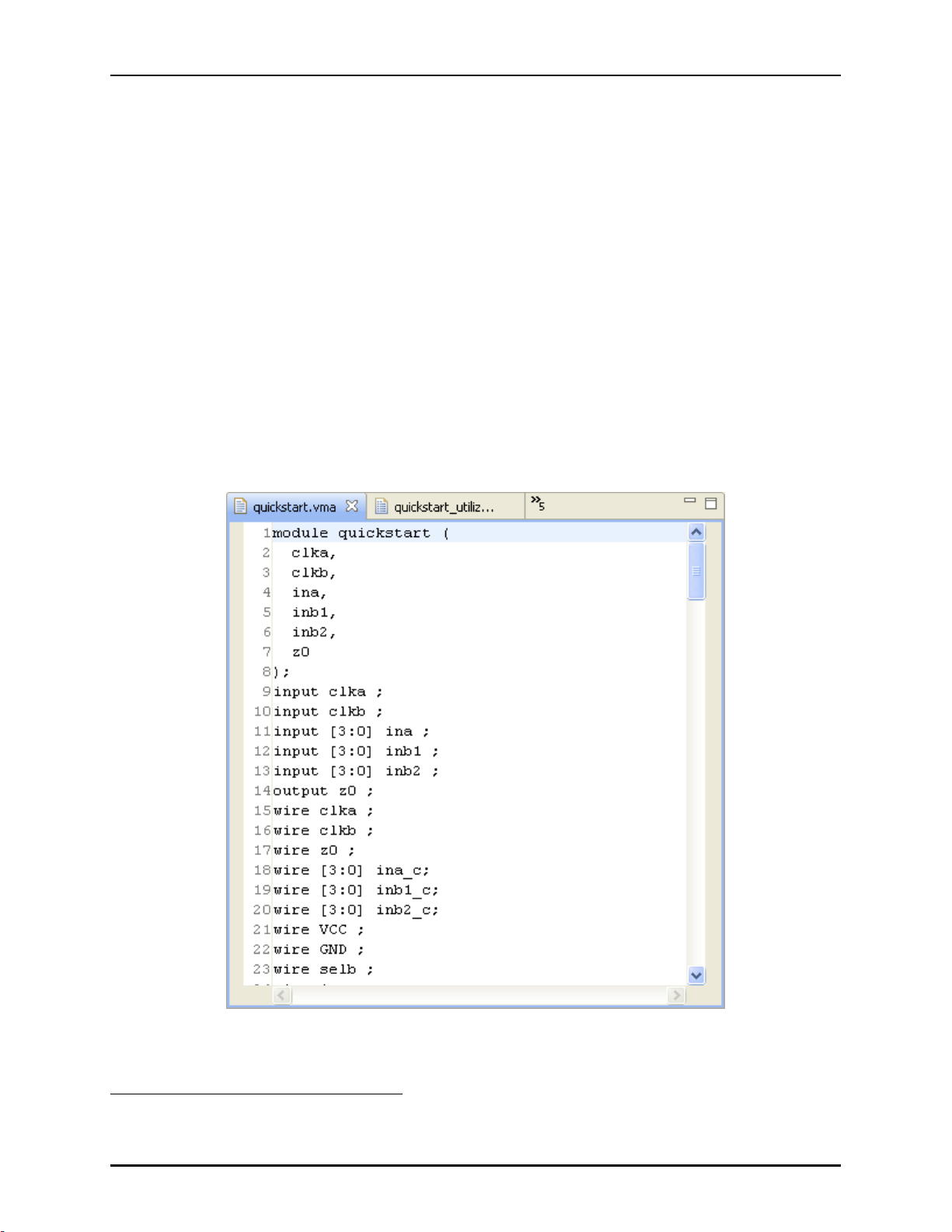
Figure 3.1: Text Editor Window
2
This is only true when running the Flow in single-process mode. In Multiprocess mode (via the Multiprocess View), only the
Multiprocess Summary Report is automatically opened in the editor area the other reports must be opened manually through the
Projects View.
UG001 Rev. 5.0 - 5th December 2012 http://www.achronix.com 6
Page 19

Editors Chapter 3. Concepts
HTML Report Browser
When HTML versions of generated Reports are opened within ACE, they are displayed within the Editor
area using the HTML Report Browser. This is a very limited form of a web browser - it only allows hyperlink
traversal, refresh, forward, and back operations.
Note:
The HTML Report Browser should typically not be used to browse the Internet - a
dedicated web browser like Firefox would be a much better choice for both security and
performance reasons.
Icon Action
Refresh
Back
Forward
HTML Report Browser Toolbar Buttons
3
Description
Refreshes the displayed HTML report to show the current contents of the
report file on disk.
Returns to the last HTML location viewed.
Returns to the HTML location viewed before the Back button was
selected. (The Forward button remains disabled until the Back button has
been pressed.)
3
These buttons are displayed in the topmost button-bar of ACE, not within the Editor area itself.
7 http://www.achronix.com UG001 Rev. 5.0 - 5th December 2012
Page 20
Editors Chapter 3. Concepts
Advanced PLL Configuration Editor
The Advanced PLL Configuration Editor provides a graphical wizard for creating a PLL configuration
file (.acxip). This editor allows the user to generate the required configuration files for design with the
embedded PLLs. See Creating an IP Configuration. Unlike the much simpler Basic PLL Configuration
Editor, the Advanced PLL Configuration Editor allows the user to access the complete functionality of the
PLL.
By default, the Advanced PLL Configuration Editor is included in the IP Configuration perspective
(Window → Open Perspective → IP Configuration) ( ). The Advanced PLL configuration information is
broken up into several pages, organized by concept. While some pages are always available, many pages of
configuration options may appear or disappear depending upon whether they are relevant, based upon the
users current choices for configuration options.
Once the user has configured the PLL to meet their requirements, and the Advanced PLL Editor has
determined that there are no errors in the configuration, the user may choose to generate their IP design
files (see Generating the IP Design Files).
IP Diagram
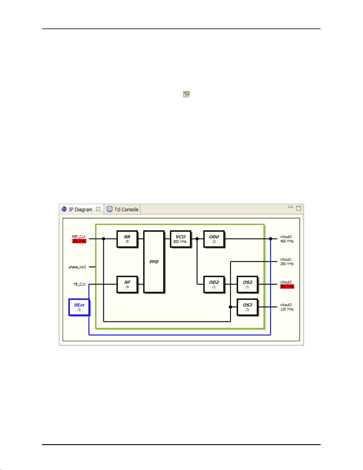
The IP Diagram View for the PLL shows live information about the current configuration in the Editor,
including which logic blocks are currently active, which inputs and outputs are currently active, and what
the various frequencies are within the PLL. Additionally, configuration errors will be shown with a red
background, and configuration warnings will be shown with a yellow background (these are the default IP
Diagram colors, and may be modified in the Preferences).
Figure 3.2: Example IP Diagram for Advanced PLL Editor with some errors in red
UG001 Rev. 5.0 - 5th December 2012 http://www.achronix.com 8
Page 21
Editors Chapter 3. Concepts
Overview Page
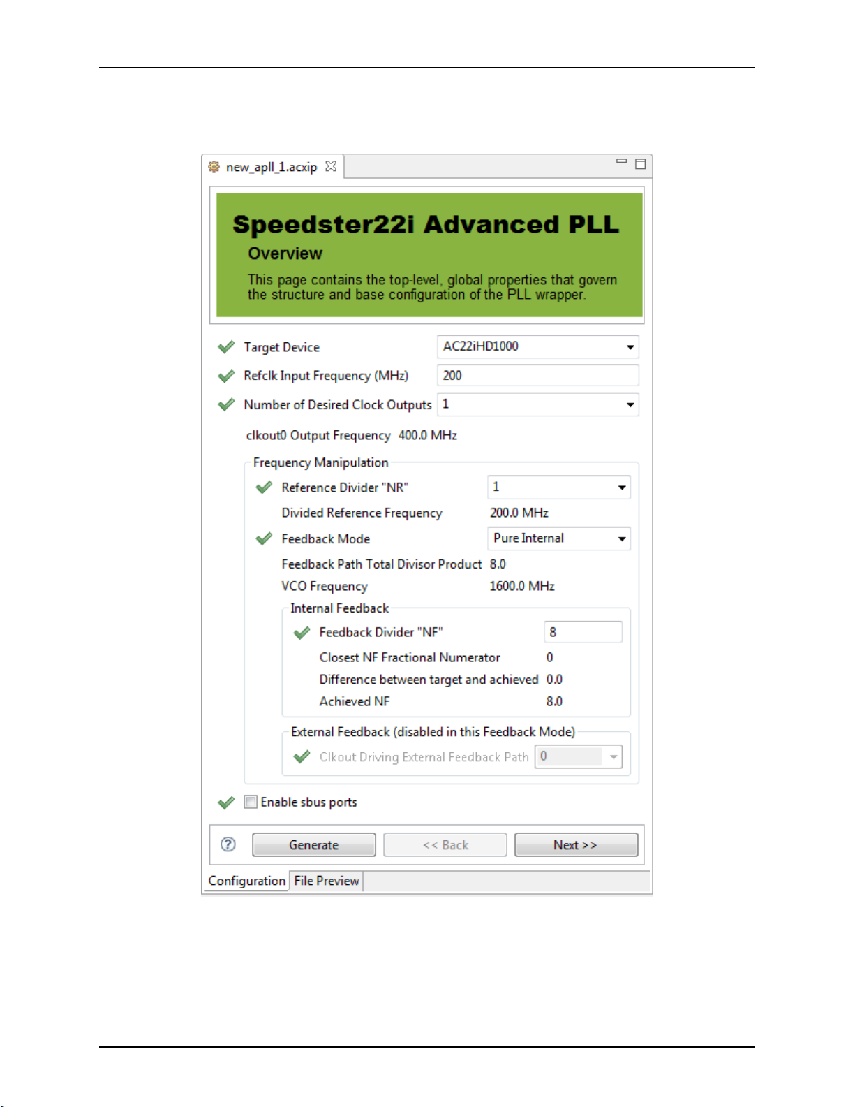
The Overview page contains the top-level, global properties that govern the structure and base
configuration of the PLL. Changes made on this page affect all the outputs for this PLL.
Figure 3.3: Advanced PLL IP Editor Overview Page
9 http://www.achronix.com UG001 Rev. 5.0 - 5th December 2012
Page 22

Editors Chapter 3. Concepts
PLL Editor Overview Page Options
Option Editable
Target Device Y
Refclk Input
Frequency (MHz)
Number of Desired
Clock Outputs
Y
Y
clkout Output
Frequency
Reference Divider
”NR”
Y
Divided Reference
Frequency
Feedback Mode Y
Description
The Speedster22i device this PLL is intended to target.
The frequency of the PLL reference clock input.
The number of desired clock output signals for this PLL.
Changing this will alter the number of active pages of
Clock Output configuration options.
The calculated output frequency of the named clock
output signal. The number of outputs listed will match
the ”Number of Desired Clock Outputs”.
The amount by which the reference clock frequency
should be divided before entering the PLLs Phase
Frequency Detector. As this value increases, the ”VCO
Frequency” decreases.
The calculated reference clock frequency after having
been divided by the ”Reference Divider ’NR’”.
Selects one of the three allowed feedback modes, and
enables/disables related options on this page according
to the selected mode. See Feedback Modes below for
more details.
Feedback Path Total
Divisor Product
VCO Frequency
Feedback Divider
”NF”
Closest NF Fractional
Numerator
Difference between
target and achieved
The calculated total product of all divisors in the present
feedback path.
The calculated VCO output frequency. The algorithm
used will vary depending upon the selected Feedback
Mode.
Y
The amount by which the feedback signal should be
divided before entering the PLLs Phase Frequency
Detector. As this value increases, the ”VCO Frequency”
increases. When in Pure Internal Feedback Mode, this
may be a floating-point value; in Mixed feedback mode
this must be an integer value. In Pure External Feedback
Mode, this option will be disabled.
This calculated values represents the fractional portion of
the entered ”Feedback Value ’NF’” used to configure the
PLL. When floating point values are entered for the
”Feedback Divider ’NF’”, they must be represented as
fractions of 65536 (a 16-bit representation of the fraction is
used). The value displayed provides the closest possible
fraction to that requested by the user.
This calculated value shows how close the PLL can come
to the requested ”Feedback Divider ’NF’” value. (Some
requested fractional values are impossible to exactly
represent within the 16 bits available in the PLL.)
UG001 Rev. 5.0 - 5th December 2012 http://www.achronix.com 10
Page 23

Editors Chapter 3. Concepts
Achieved NF
This calculated value shows the exact ”Feedback Divider
’NF’” value which will be used by the PLL. This may
differ slightly from the requested value; the closest
approximate value will be chosen if an exact match is not
possible.
Clkout Driving
External Feedback
Path
Y
Selects which of the currently-enabled clock outputs will
drive the external feedback path. Note that Phase
Adjustment is not allowed in the Feedback Path.
Enable sbus ports Y
When selected, the sbus ports will be exposed in the
generated HDL file(s).
Feedback Modes There are three feedback modes available to the PLL. Some allow fractional feedback,
others allow deskew.
PLL Feedback Modes
Mode Fractional Feedback? Deskew?
Pure Internal Y N
Pure External N Y
Mixed N Y
Algorithm
F
=(NF/NR)*F
V CO
F
=(ODn*OSn/NR)*F
V CO
F
=(NF*ODn*OSn/NR)*F
V CO
ref
ref
ref
Pure Internal Feedback
When internal feedback mode is selected, the VCO clock is divided by the ”Feedback Divider ’NF’” only.
In this mode, the PLL can have both integer and fractional feedback divider values. The ”Clkout Driving
External Feedback Path” option becomes disabled in this mode, since it is irrelevant. Deskewing is not
possible in this mode.
Pure External Feedback
When external feedback mode is selected, the VCO clock is divided by the Output Divider (ODn) and
(optionally) the Output Synthesizer (OSn). The ”Clkout Driving External Feedback Path” option becomes
enabled in this mode, and the ”Feedback Divider ’NF’” option becomes disabled. In this mode, it is not
allowed to feedback a clock output that has Phase Adjustment enabled.
4
Mixed Feedback
Mixed feedback mode is a modified version of Pure External feedback mode, in that the Feedback Divider
integer value is also in the deskew feedback path. As with Pure External mode, Phase Adjustment is not
allowed in the feedback path. The ”Clkout Driving External Feedback Path” option becomes enabled in this
mode, as does ”Feedback Divider ’NF’”.
4
Phase rotation in the feedback path will cause the PLL to unlock. If Phase Adjustment is required on any output clocks, it must be
used on outputs which are not in the feedback path.
11 http://www.achronix.com UG001 Rev. 5.0 - 5th December 2012
Page 24
Editors Chapter 3. Concepts
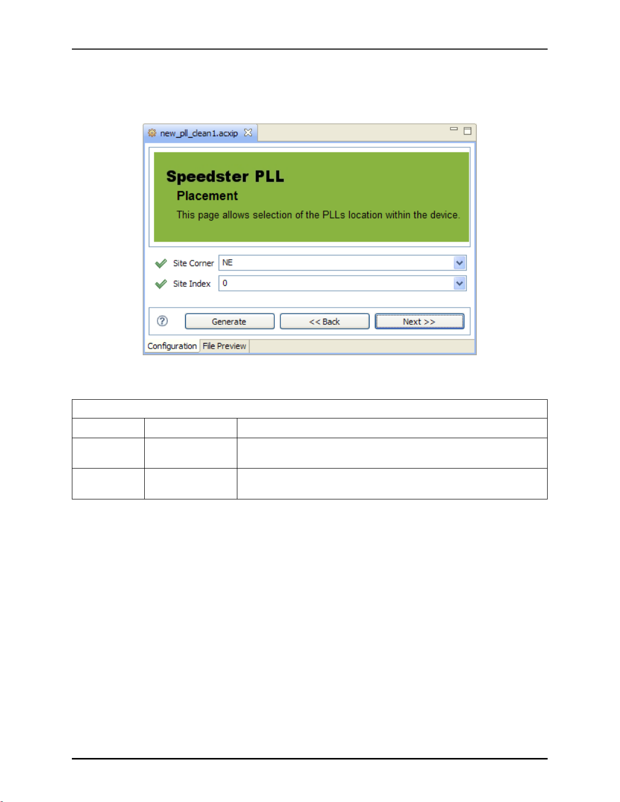
Placement Page
The Placement page contains configuration information relating to the PLLs placement in the Speedster
device. The site chosen will be exported in a placement constraints (.pdc) file when the user chooses to
generate their PLL design files.
Option Editable
Site Corner Y
Site Index Y
Figure 3.4: Advanced PLL IP Editor Placement Page
PLL Editor Placement Page Options
Description
The corner of the Speedster22i device where this PLL instance
should be placed. The four choices are NE, SE, SW, and NW.
The site index within the corner where this PLL instance should be
placed.
UG001 Rev. 5.0 - 5th December 2012 http://www.achronix.com 12
Page 25
Editors Chapter 3. Concepts
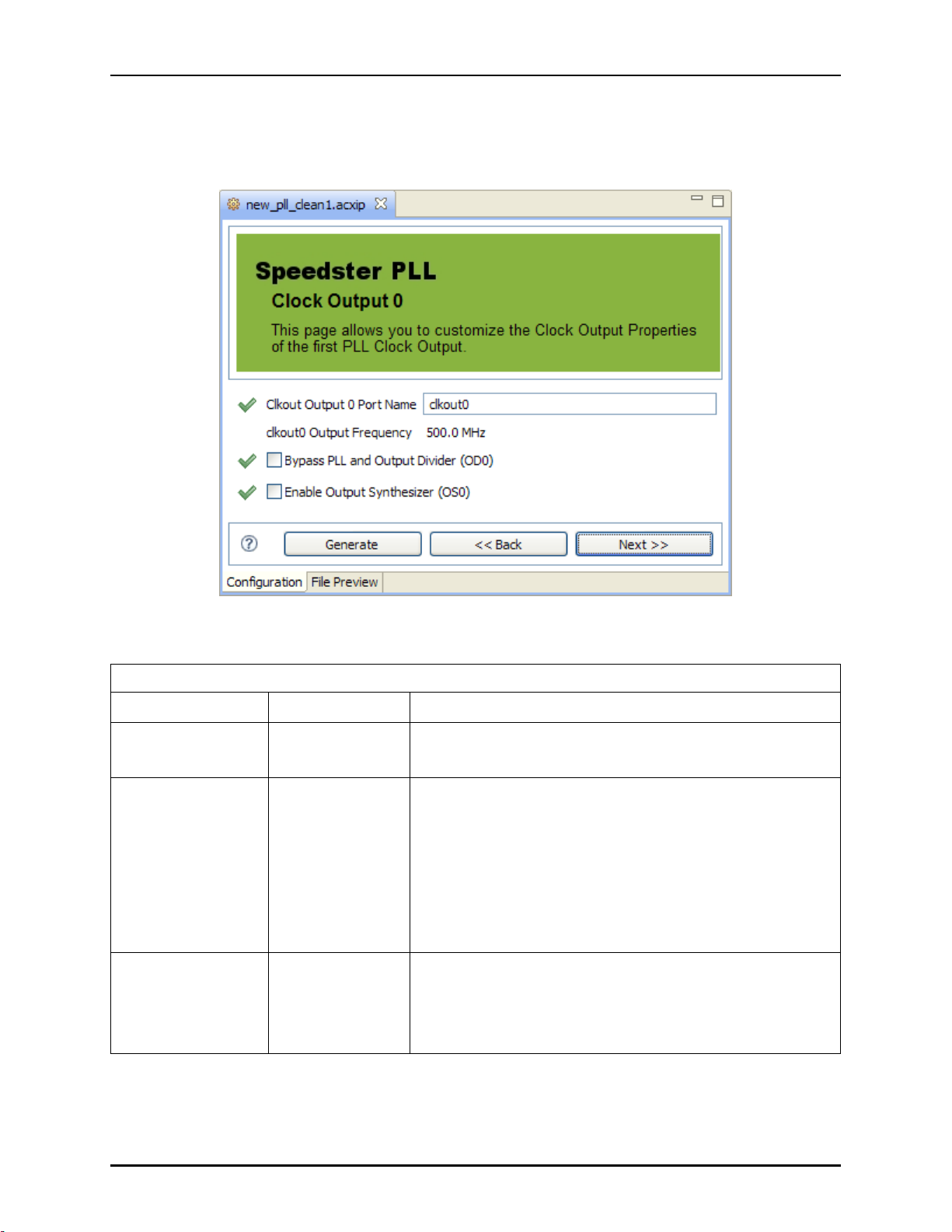
Clock Output [0,1,2,3] Pages
The Clock Output pages each contain general configuration information relating to a single PLL output
signal. Since there are one-to-four PLL output signals per PLL (as configured on the Overview Page),
between one and four Clock Output pages will be enabled.
Figure 3.5: IP Advanced PLL Editor Clock Output 0 Page
Option Editable
clkout Output
Frequency
Bypass PLL and
Output Divider
(OD[0-3])
Enable Output
Synthesizer
(OS[0-3])
Y
Y
PLL Editor Clock Output Page Options
Description
The calculated frequency of this clock output signal as it
exits the PLL.
Enabling this will bypass the NR, PFD, VCO, and OD,
sending the reference clock input signal directly to the OS
input. Disabling this allows normal PLL behavior. Note that
when this is enabled, the IP Editor configuration page for
the Output Divider (OD) associated with this clock output is
disabled. In addition, when enabled, it becomes illegal to
use this output in an external feedback path, as the PLL will
lose lock.
Allows this clock output to use its Output Synthesizer (OS).
When enabled, this activates the IP Editor configuration
page for the OS associated with this clock output. When
disabled, the associated OS configuration page is hidden.
13 http://www.achronix.com UG001 Rev. 5.0 - 5th December 2012
Page 26
Editors Chapter 3. Concepts
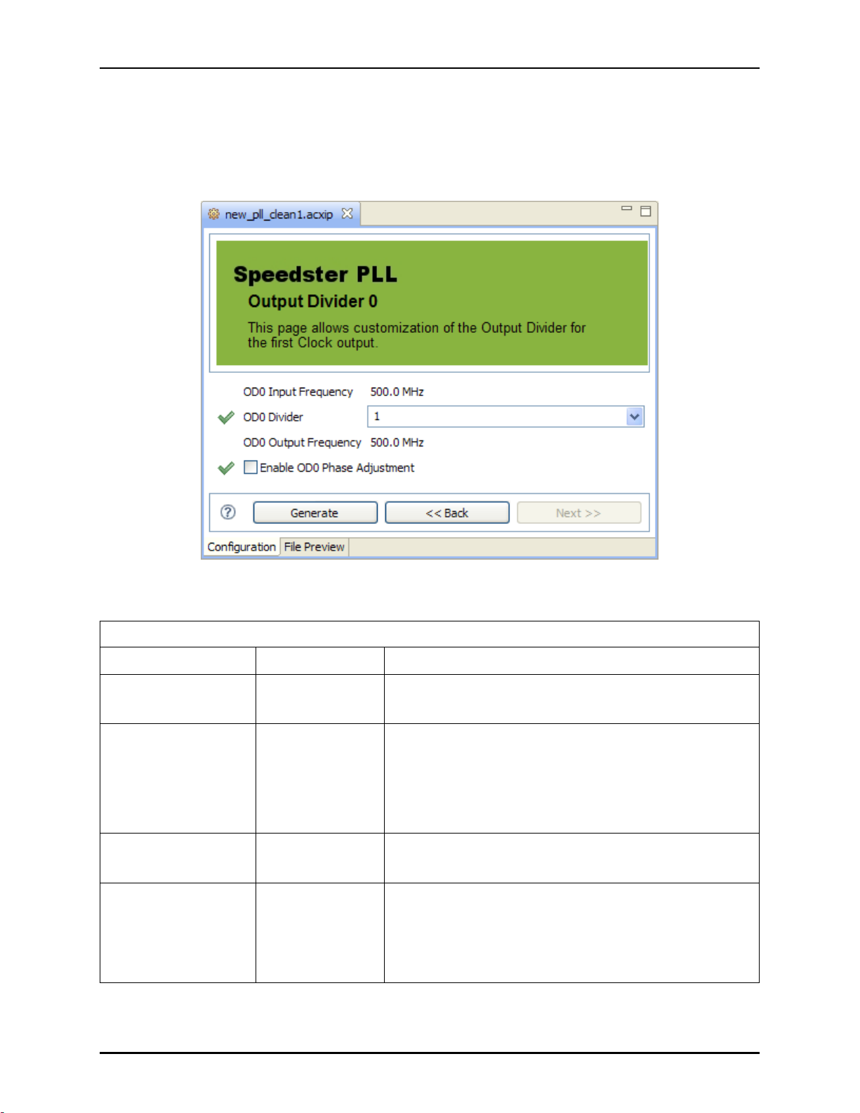
Output Divider [0,1,2,3] Pages
The Output Divider pages contain configuration information relating to the output divider (OD) of one of
the PLLs clock output signals. Since there are one-to-four PLL output signals per PLL, there are also up to
four of these pages. Because the PLL and OD logic may be bypassed on a per-output basis (as configured
on the Clock Output [0,1,2,3] Pages), this page may sometimes be hidden, even if the related clock output is
enabled.
Figure 3.6: IP Advanced PLL Editor Output Divider 0 Page
PLL Editor Output Divider Page Options
Option Editable
OD[0-3] Input
Frequency
OD[0-3] Divider Y
OD[0-3] Output
Frequency
Enable OD[0-3] Phase
Adjustment
Y
Description
The calculated frequency of the input signal as it enters
this OD logic block.
The factor by which the signal entering the OD should be
divided before it exits the OD. As this increases, the OD
output frequency decreases. (Unless this OD is in the
external feedback path, in which case increasing this
value does not affect the OD output frequency, but
increases the VCO output frequency.)
The calculated frequency of the output signal as it exits
this OD logic block.
Enabling this will allow this OD to perform phase
adjustments on the OD output signal. When enabled, this
activates the related OD [0,1,2,3] Phase Adjustment Pages.
When disabled, the phase adjustment configuration
options remain hidden.
UG001 Rev. 5.0 - 5th December 2012 http://www.achronix.com 14
Page 27
Editors Chapter 3. Concepts
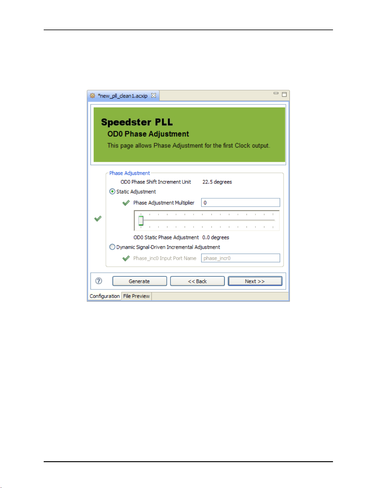
OD [0,1,2,3] Phase Adjustment Pages
The Output Divider (OD) Phase Adjustment pages contain configuration information about the potential
phase adjustment performed in an OD for one of the PLLs clkout signals. This page will only be visible
when the associated Output Divider [0,1,2,3] Pages are enabled, and the setting ”Enable OD[0-3] Phase
Adjustment” is selected. There is potentially one of these pages associated with every OD, so there will be
between zero and four of these pages for a given IP configuration.
Figure 3.7: IP Advanced PLL Editor OD0 Phase Adjustment Page
15 http://www.achronix.com UG001 Rev. 5.0 - 5th December 2012
Page 28

Editors Chapter 3. Concepts
PLL Editor OD Phase Adjustment Options
Option Editable
OD[0-3] Phase Shift
Increment Unit
Static Adjustment Y
Phase Adjustment Multiplier Y
OD[0-3] Static Phase
Adjustment
Dynamic Signal-Driven
Incremental Adjustment
Y
Description
The incremental step, always 45 degrees, by which
the OD output signal will be shifted relative to the
VCO output signal. This is a fixed value, displayed
for user convenience.
When selected, a single, unchanging phase
adjustment must be chosen for this OD. When this
is enabled, the ”Phase Adjustment Multiplier” field
will also be enabled.
This value is multiplied by the ”OD[0-3] Phase
Shift Increment Unit” to determine the total
”OD[0-3] Static Phase Adjustment”.
The calculated total phase shift, in degrees,
performed by this OD.
When selected, this enables dynamic phase
adjustment mode, where the phase of the OD
output signal will advance by ”OD[0-3] Phase Shift
Increment Unit” degrees each time a rising edge is
applied to the associated phase inc input signal.
When this mode is enabled, the ”Phase
Adjustment Multiplier” field will be disabled.
UG001 Rev. 5.0 - 5th December 2012 http://www.achronix.com 16
Page 29
Editors Chapter 3. Concepts
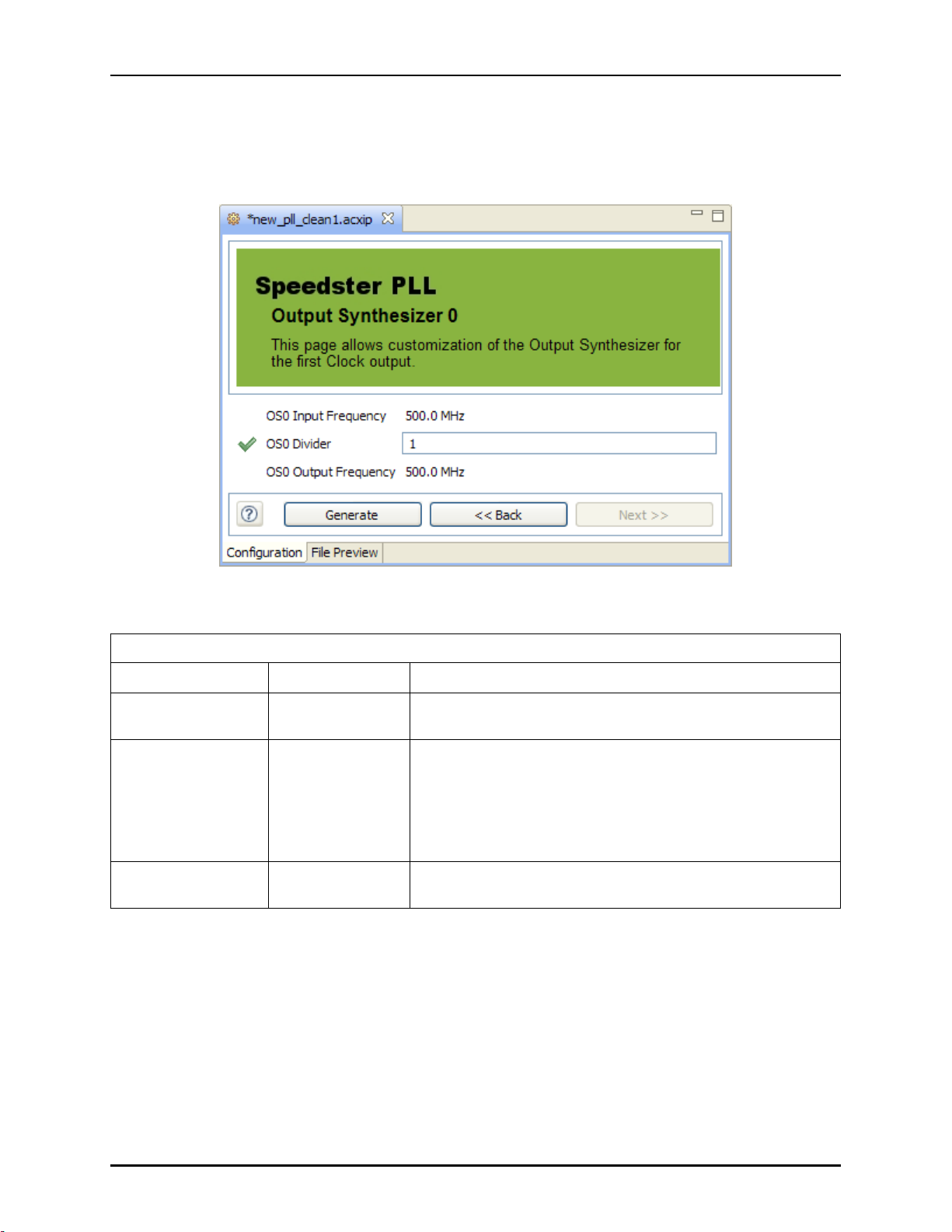
Output Synthesizer [0,1,2,3] Pages
The Output Synthesizer (OS) pages contain configuration information relating to the OS associated with
the PLLs selected clock output. Because the OS can be disabled for a PLL clock output, this page is only
visible when the ”Enable Output Synthesizer (OS[0-3])” field on the appropriate Clock Output [0,1,2,3] Page
is enabled.
Figure 3.8: IP Advanced PLL Editor Output Synthesizer 0 Page
PLL Editor Output Synthesizer Page Options
Option Editable
OS[0-3] Input
Frequency
OS[0-3] Divider Y
OS[0-3] Output
Frequency
Description
The calculated frequency of the OS input signal.
The factor by which the signal entering the OS should be
divided before it exits the OS. As this increases, the OS
output frequency decreases. (Unless this OS is in the
external feedback path, in which case increasing this value
does not affect the OS output frequency, but instead
increases the VCO output frequency.)
The calculated frequency of the OS output signal.
17 http://www.achronix.com UG001 Rev. 5.0 - 5th December 2012
Page 30
Editors Chapter 3. Concepts
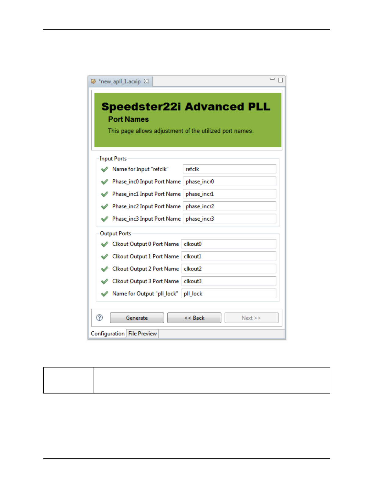
Port Names Page
The Port Names page contains all the input and output ports which will be used by the PLL in its current
configuration. (Changing options on other pages will show and hide port names on this page, as the need
for the ports changes.)
Figure 3.9: IP Advanced PLL Editor Port Names Page
NOTE:
UG001 Rev. 5.0 - 5th December 2012 http://www.achronix.com 18
All port names entered on this page must adhere to Verilog and VHDL naming
standards. Illegal names will be caught as errors, and will prohibit RTL wrapper file
generation.
Page 31

Editors Chapter 3. Concepts
Advanced PLL Editor Port Names Page Options
Option Description
Input Ports
Name for Input ”refclk” The desired name for the reference clock input
signal in the generated RTL.
Name for Input ”fbclk” The desired name for the feedback clock input
signal in the generated RTL. This option is not
available when the PLL is in Pure Internal
Feedback Mode.
Phase inc[0-3] Input Port Name The desired name for the phase inc input signal
(for the appropriately numbered clock output) in
the generated RTL.
Output Ports
Clkout Output [0-3] Port Name The desired name for the PLL clock output in the
generated RTL.
Name for Output ”pll lock” The desired name for the PLL’s lock indication
output signal in the generated RTL.
19 http://www.achronix.com UG001 Rev. 5.0 - 5th December 2012
Page 32

Editors Chapter 3. Concepts
Basic PLL Configuration Editor
The Basic PLL Configuration Editor provides a simplified graphical wizard for creating a PLL configuration
file (.acxip). This editor allows the user to generate the required configuration files for design with the
embedded PLLs. See Creating an IP Configuration. Unlike the much more complicated Advanced PLL
Configuration Editor, the Basic PLL Configuration Editor allows the user to access only the most-often used
functionality of the PLL.
By default, the Basic PLL Configuration Editor is included in the IP Configuration perspective
(Window→Open Perspective→IP Configuration) ( ). The Basic PLL configuration information fits into a
single page.
Once the user has configured the PLL to meet their requirements, and the Basic PLL Configuration Editor
has determined that there are no errors in the configuration, the user may choose to generate their IP design
files (see Generating the IP Design Files).
NOTE:
IP Diagram
The IP Diagram View for the Basic PLL shows live information about the current configuration in the Editor,
including which logic blocks are currently active, which inputs and outputs are currently active, and what
the various frequencies are within the PLL. Additionally, configuration errors will be shown with a red
background, and configuration warnings will be shown with a yellow background (these are the default IP
Diagram colors, and may be modified in the Preferences).
The Basic PLL only supports Pure Internal Feedback Mode, and thus hides feedback path
modes from the user. This allows fractional feedback dividers (so any desired clkout0
output frequency is achievable), but prohibits deskew functionality. For simplification,
output phase adjustment is also disabled. If deskew or phase adjustment functionality are
required, the Advanced PLL must be used instead of the Basic PLL.
Figure 3.10: Example IP Diagram for PLL
UG001 Rev. 5.0 - 5th December 2012 http://www.achronix.com 20
Page 33

Editors Chapter 3. Concepts
Overview Page
The Overview page contains all the properties that govern the structure and configuration of the basic PLL.
Figure 3.11: Basic PLL IP Editor Overview Page
PLL Editor Overview Page Options
Option Editable
Target Device Y
Number of
Desired Clock
Outputs
Refclk Input
Frequency
(MHz)
21 http://www.achronix.com UG001 Rev. 5.0 - 5th December 2012
Y
Y
Description
The Speedster22i device this PLL is intended to target.
The number of desired clock output signals for this PLL.
Changing this will alter the number of active pages of Clock
Output configuration options.
The frequency of the PLL reference clock input.
Page 34

Editors Chapter 3. Concepts
clkout0 Desired
Frequency
Y
clkout0
Achieved
Frequency
VCO
Frequency
Additional Clkout Outputs
clkout[1-3]
Desired
Y
Divider
clkout[1-3]
Output
Frequency
The frequency desired for clkout0. ACE will automatically
choose PLL configuration values (NR, NF, OD0, OS0) to get as
close to the desired frequency as possible.
The calculated output frequency of the clkout0 clock output
signal. This will be as close to the ”clkout0 Desired Frequency”
as possible.
The calculated VCO output frequency which was required to
achieve the requested clkout0 frequency. This will also be used
to drive any other enabled clkout outputs.
The requested divider to use to alter the VCO Frequency for the
clkout output. Some values in the allowed range are not
achievable - in these cases, a warning is reported and the closest
divider is used instead. Changing this option value will change
the associated clkout Output Frequency.
The achieved output frequency of the named output. This will
vary according to the VCO Frequency and the clkout Desired
Divider.
Placement
Site Corner Y
Site Index Y
The corner of the Speedster22i device where this PLL instance
should be placed. The four choices are NE, SE, SW, and NW.
The site index within the corner where this PLL instance should
be placed.
UG001 Rev. 5.0 - 5th December 2012 http://www.achronix.com 22
Page 35

Editors Chapter 3. Concepts
BRAM Configuration Editor
The BRAM Configuration Editor provides a simplified graphical wizard for creating a BRAM configuration
file (.acxip). This editor allows the user to generate the required configuration files for design with the
embedded PLLs. See Creating an IP Configuration.
By default, the BRAM Configuration Editor is included in the IP Configuration perspective
(Window→Open Perspective→IP Configuration) ( ). The BRAM configuration information fits into a
single page, unlike more complicated IP editors.
Once the user has configured the BRAM to meet their requirements, and the BRAM Configuration Editor
has determined that there are no errors in the configuration, the user may choose to generate their IP design
files (see Generating the IP Design Files).
IP Diagram
The IP Diagram View for the BRAM shows live information about the current configuration in the Editor,
including which inputs and outputs are currently active.
Figure 3.12: Example IP Module Diagram for BRAM
23 http://www.achronix.com UG001 Rev. 5.0 - 5th December 2012
Page 36

Editors Chapter 3. Concepts
Overview Page
The Overview page contains all the properties that govern the structure and configuration of the BRAM
wrapper.
BRAM Editor Overview Page Options
Option
Port A
Port A Configuration
Data Width
Address Depth
Write Mode
Editable
Y
Y
Y
Y
Description
BRAMs can be configured for read, write, or
read/write capability independently on both
Port A and Port B sides of the BRAM.
Port A side write and read port data width.
We currently only support Port A data width
being a ratio of 1:2n or 2n:1 with Port B data
width. The max ratio is 1:32 or 32:1. This
field imposes limitations on the Port B side
data width and address depth.
Port A side address depth is the total number
of data words accessible via Port A. This field
imposes limitations on the Port B side data
width and address depth. The Port B data
width must be a valid integer ratio of the
Port A data width.
The write mode can be set to No Change in
order to keep the read port value constant
until the next read. It can be set to Write First
to allow the write data to be seen on the read
port before the next read.
Clock Polarity
Port Enable Active-High
Output Latch Reset Active-High
Output Register Enabled
Output Register
Y
The write port clock polarity can be set to use
either rising edge assignment or falling edge
assignment.
Y
When this is enabled, the port enable pea is
active-high. Otherwise, the port enable will
be active-low.
Y
When this is enabled, the output latch has an
active-high synchronous reset. Otherwise,
the output latch reset will be active-low.
Y
When the Output Register is enabled, there is
an additional cycle of latency for each read
operation.
UG001 Rev. 5.0 - 5th December 2012 http://www.achronix.com 24
Page 37

Editors Chapter 3. Concepts
Clock Enable Priority Y
Output Register Reset
Active-High
Port B
Port B Configuration
Data Width
The Clock Enable Priority defines the priority
of the outregcea clock enable input relative to
the rstrega reset input during an assertion of
the rstrega signal on the output register of
Port A. The value rstreg allows the Port A
output register to be set/reset at the next
active edge of the Port A clock without
requiring a specific value on the outregcea
output register clock enable input. The value
regce requires that the outregcea output
register clock enable input is high for the
output register set/reset operation to occur at
the next active edge of the Port A clock.
Y
When this is enabled, the output register has
an active-high synchronous reset. Otherwise,
the output register reset will be active-low.
Y
BRAMs can be configured for read, write, or
read/write capability independently on both
Port A and Port B sides of the BRAM.
Y
Port A side write and read port data width.
We currently only support Port A data width
being a ratio of 1:2n or 2n:1 with Port B data
width. The max ratio is 1:32 or 32:1. This
field imposes limitations on the Port B side
data width and address depth.
Address Depth Port A side address depth is the total number
of data words accessible via Port A. This field
imposes limitations on the Port B side data
width and address depth. The Port B data
width must be a valid integer ratio of the
Port A data width.
Write Mode
Y
The write mode can be set to No Change in
order to keep the read port value constant
until the next read. It can be set to Write First
to allow the write data to be seen on the read
port before the next read.
Clock Polarity
Y
The write port clock polarity can be set to use
either rising edge assignment or falling edge
assignment.
Port Enable Active-High
Y
When this is enabled, the port enable peb is
active-high. Otherwise, the port enable will
be active-low.
Output Latch Reset Active-High
Y
When this is enabled, the output latch has an
active-high synchronous reset. Otherwise,
the output latch reset will be active-low.
Output Register Enabled
Y
When the Output Register is enabled, there is
an additional cycle of latency for each read
operation.
25 http://www.achronix.com UG001 Rev. 5.0 - 5th December 2012
Page 38

Editors Chapter 3. Concepts
Output Register
Clock Enable Priority Y
Output Register Reset
Active-High
Total Memory Size Port A Address Depth x Port A Data Width
Number of BRAMs Used The total number of BRAM instances which
Y
The Clock Enable Priority defines the priority
of the outregceb clock enable input relative
to the rstregb reset input during an assertion
of the rstregb signal on the output register of
Port B. The value rstreg allows the Port B
output register to be set/reset at the next
active edge of the Port B clock without
requiring a specific value on the outregceb
output register clock enable input. The value
regce requires that the outregceb output
register clock enable input is high for the
output register set/reset operation to occur at
the next active edge of the Port B clock.
When this is enabled, the output register has
an active-high synchronous reset. Otherwise,
the output register reset will be active-low.
will be used to create a BRAM wrapper of the
configured width(s) and depth(s).
UG001 Rev. 5.0 - 5th December 2012 http://www.achronix.com 26
Page 39

Editors Chapter 3. Concepts
Figure 3.13: BRAM IP Editor Overview Page
27 http://www.achronix.com UG001 Rev. 5.0 - 5th December 2012
Page 40

Editors Chapter 3. Concepts
DDR3 Configuration Editor
The DDR3 Configuration Editor provides a graphical wizard for creating a DDR3 Interface IP configuration
file (.acxip). This editor allows the user to generate the required configuration files for designs requiring the
embedded DDR3 controllers. See Creating an IP Configuration.
By default, the DDR3 Configuration Editor is included in the IP Configuration perspective (Window→Open
Perspective→IP Configuration) ( ). The DDR3 Interface configuration information is broken up into
several pages, organized by concept.
Once the user has configured the DDR Interface to meet their requirements, and the DDR3 Configuration
Editor has determined that there are no errors in the configuration, the user may choose to generate their IP
design files (see Generating the IP Design Files).
DDR3 IP Diagrams Note that the DDR3 Configuration Editors support two subtabs in the IP Diagram
View: a Module tab showing the detailed DDR3 Interface based upon the current configuration, and a
Placement tab showing the placement of the DDR3 Controller within the chosen ”Target Device”, as selected
on the Overview Page. Both of these diagram tabs will update on-the-fly to match the current DDR3
configuration in the editor pages.
UG001 Rev. 5.0 - 5th December 2012 http://www.achronix.com 28
Page 41

Editors Chapter 3. Concepts
Figure 3.14: A Module diagram for DDR3 in the IP Diagram View
29 http://www.achronix.com UG001 Rev. 5.0 - 5th December 2012
Page 42

Editors Chapter 3. Concepts
Figure 3.15: A Placement diagram for DDR3 in the IP Diagram View.
UG001 Rev. 5.0 - 5th December 2012 http://www.achronix.com 30
Page 43

Editors Chapter 3. Concepts
Overview Page
The Overview page contains the top-level, global properties that govern the structure and base
configuration of the DDR3 Interface.
Figure 3.16: DDR3 IP Editor Overview Page
31 http://www.achronix.com UG001 Rev. 5.0 - 5th December 2012
Page 44

Editors Chapter 3. Concepts
DDR3 Editor Overview Page Options
Option
Target Device
Placement
Clock Pin
Name
DIMM Type
Data Rate
(Mbps)
Fabric Interface
Width
Data Width
Number of
CLKOUTs
Number of
Ranks
Address
Command
Delay (hex)
Description
Allows the user to select from the Achronix devices that support this IP.
Select the location on the chip where this DDR interface should be placed.
Enter the reference clock pin name. Will be used to generate clock constraints. May be
a top level design pin, a PLL clock output pin, etc.
Select from a predefined library of standard DIMMs, or select Custom for full
customization options.
May be configured to use a standard rate, or may be customized.
Wide fabric (core) interface widths running at half speed are needed to achieve the
highest speed Data Rate values.
Local side data width.
Number of DDR3 DIMM clocks.
Number of chip selects used.
The number of pipe stages in the address and command path.
Enable Address
Mirroring
Enable Wide
Bus Interface
DIMM Settings
Number of
Column Bits
Number of
Row Bits
Number of
Bank Bits
DQ Per DQS
Registered
DIMM
Enable Address Mirroring in the DDR Controller.
When enabled, this doubles the width of the data bus, and helps meet timing at
higher frequencies.
Number of bits for Column Address.
Number of bits for Row Address.
Number of bits for Bank Address.
Number of DQ bits per DQS line.
Whether or not the DDR3 DIMM is registered.
UG001 Rev. 5.0 - 5th December 2012 http://www.achronix.com 32
Page 45

Editors Chapter 3. Concepts
Memory Timing Page
The Memory Timing Page allows the user to configure the memory timings for the DDR3 Interface.
DDR3 Editor Memory Timing Page Options
Option
Description
AL/CL/CWL
Additive latency value
CAS Latency
CAS Write Latency
Additive Latency (AL) in clock cycles
CAS Latency (CL) in clock cycles
CAS Write Latency (CWL) in clock cycles
Auto-Refresh
Controller Refresh Enable
Refresh Period
When enabled, the DDR Controller will handle DDR Memory Refreshes
Number of clocks between Refresh commands
Command-to-Command Delays
Activate To Activate (Diff
Bank)
Activate To Activate (Same
Bank)
Activate To Precharge
Activate To R/W
Auto-refresh To Activate
(Same Bank)
Minimum number of clock cycles from Activate to Activate in different
Banks
Minimum number of clock cycles from Activate to Activate/Auto Refresh
in the same Bank
Minimum number of clock cycles from Activate to Precharge
Minimum number of clock cycles between Activate and Read/Write
Minimum number of clock cycles from Auto Refresh to Activate/Auto
Refresh in the same Bank
Bank Activate Period
Loadmode To Activate
Loadmode To Any
Precharge To Activate
Read To Precharge
Read To Read (Diff Bank)
Read To Write
Reset High to Clock High
Self-refresh to Non-DLL
command
Self-refresh to Non-Read
command
Write To Precharge
Write To Read
Write To Read (Diff Bank)
Write To Write (Diff Bank)
Four Bank activate period
Minimum clock cycles from Loadmode to Activate command
Minimum clock cycles from Loadmode to Any command
Minimum clock cycles from Precharge to Activate
Minimum clock cycles from Read to Precharge
Minimum clock cycles from Read to Read (Different Banks)
Read to Write delay in clock cycles
Minimum clock cycles from memory reset high to cke high
Minimum clock cycles from Self-refresh to Non-DLL command
Minimum clock cycles from Self-refresh to Non-Read command
Minimum clock cycles from write to Precharge
Minimum clock cycles from Write to Read
Minimum clock cycles from Write to Read (Different Banks)
Minimum clock cycles from Write to Write (Different Banks)
33 http://www.achronix.com UG001 Rev. 5.0 - 5th December 2012
Page 46

Editors Chapter 3. Concepts
Figure 3.17: DDR3 IP Editor Memory Timing Page
UG001 Rev. 5.0 - 5th December 2012 http://www.achronix.com 34
Page 47

Editors Chapter 3. Concepts
DLL Timing Page
The DLL Timing Page allows the user to configure the DLL timing parameters for the DDR3 Interface.
DDR3 Editor DLL Timing Page Options
Option
DP Slave
Adjust for
CAC Byte
Lanes
Byte Lane N
DQ Slave
Adjust
DQS Slave
Adjust
DP Slave
Adjust
Write Level
DQ Bit
Description
DP Slave Adjust for CAC Byte Lanes
5
DLL delay adjust value for all DQ bits in this byte lane
DLL delay adjust value for all DQS lines in this byte lane
DLL delay adjust value for DP line in this byte lane
DQ bit used for write leveling in this byte lane
5
There are multiple sets of these on the page, one set for each Byte Lane.
35 http://www.achronix.com UG001 Rev. 5.0 - 5th December 2012
Page 48

Editors Chapter 3. Concepts
Figure 3.18: DDR3 IP Editor DLL Timing Page
UG001 Rev. 5.0 - 5th December 2012 http://www.achronix.com 36
Page 49

Editors Chapter 3. Concepts
On-Die Termination Page
The On-Die Termination Page allows the user to configure the On-Die Termination parameters for the DDR3
Interface.
Figure 3.19: DDR3 IP Editor On-Die Termination Page
37 http://www.achronix.com UG001 Rev. 5.0 - 5th December 2012
Page 50

Editors Chapter 3. Concepts
DDR3 Editor On-Die Termination Page Options
Option
ODT Selection for Reads
ODT Read
CS0
ODT Read
CS1
. . .
ODT Read
CS7
ODT Selection for Writes
ODT Write
CS0
ODT Write
CS1
. . .
ODT Write
CS7
Description
Enable/Disable On-Die Termination for READS on Chip Select 0
Enable/Disable On-Die Termination for READS on Chip Select 1
. . .
Enable/Disable On-Die Termination for READS on Chip Select 7
Enable/Disable On-Die Termination for WRITES on Chip Select 0
Enable/Disable On-Die Termination for WRITES on Chip Select 1
. . .
Enable/Disable On-Die Termination for WRITES on Chip Select 7
UG001 Rev. 5.0 - 5th December 2012 http://www.achronix.com 38
Page 51

Editors Chapter 3. Concepts
Ethernet Configuration Editor
The Ethernet interface configuration editor provides a simple graphical editor used to configure the SerDes
interface for the Ethernet protocol, and saves the user configuration in an Ethernet IP configuration file
(.acxip). See Creating an IP Configuration.
By default, the Ethernet Configuration Editor is included in the IP Configuration perspective
(Window→Open Perspective→IP Configuration) ( ). The Ethernet interface configuration information
fits into a single page.
Once the user has configured the Ethernet interface to meet their requirements, and the Ethernet
Configuration Editor has determined that there are no errors in the configuration, the user may choose
to generate their IP design files (see Generating the IP Design Files).
IP Diagrams
Note that the Ethernet Configuration Editors support two subtabs in the IP Diagram View: a Module tab
showing the detailed DDR3 Interface based upon the current configuration, and a Placement tab showing
the placement of the DDR3 Controller within the chosen ”Target Device”, as selected on the Overview Page.
Both of these diagram tabs will update on-the-fly to match the current DDR3 configuration in the editor
pages.
The example Placement Diagram shows an Ethernet instance placed in MAC1, containing a single 100G
interface and a single 10G interface, separated by an empty lane.
Figure 3.20: Ethernet IP Editor Placement Diagram
The example Module diagram shows all the inputs and outputs of the module instantiation.
39 http://www.achronix.com UG001 Rev. 5.0 - 5th December 2012
Page 52

Editors Chapter 3. Concepts
Figure 3.21: Ethernet IP Editor Module Diagram
UG001 Rev. 5.0 - 5th December 2012 http://www.achronix.com 40
Page 53

Editors Chapter 3. Concepts
Overview Page
The Overview page of the Ethernet IP Configuration Editor contains all the options that govern the structure
and configuration of the Ethernet interface.
Figure 3.22: Ethernet IP Editor Overview Page
41 http://www.achronix.com UG001 Rev. 5.0 - 5th December 2012
Page 54

Editors Chapter 3. Concepts
Ethernet Editor Overview Page Options
Option Description
Target Device Select the intended 22i Target Device. This may affect choices in other option
fields, and will affect the generated wrapper files.
Lane Configuration and Placement
Lane Configuration
MAC Block
MAC Clock Settings
MAC Ref Clock
(MHz)
MAC FIFO Clock
(MHz)
MAC System Clock
(MHz)
MAC Timestamp
Clock (MHz)
Serial Bus Clock
(MHz)
Use this field to select the placement of each lane interface with respect to the
MAC. 100G consumes a block of 10 serdes lanes, 40G consumes a block of 4
serdes lanes, and 10G consumes a single serdes lane. See the placement
diagram for more info.
There are two Ethernet MAC sites on the south side of the chip. See the
Placement tab of the IP Diagram view to see a graphical representation of the
sites.
The reference clock frequency of this Ethernet MAC (used to generate SDC).
The MAC FIFO clock frequency (used to generate SDC).
The MAC system clock frequency (used to generate SDC).
The MAC timestamp clock frequency (used to generate SDC).
The Serial Bus clock frequency of this Ethernet MAC (used to generate SDC).
UG001 Rev. 5.0 - 5th December 2012 http://www.achronix.com 42
Page 55

Editors Chapter 3. Concepts
FIFO Configuration Editor
The FIFO Configuration Editor provides a graphical wizard for creating a FIFO configuration file (.acxip).
This editor allows the user to generate the required configuration files for design with the embedded
BRAMs. See Creating an IP Configuration.
By default, the FIFO Configuration Editor is included in the IP Configuration perspective (Window→Open
Perspective→IP Configuration) ( ).
Once the user has configured the FIFO to meet their requirements, and the FIFO Editor has determined that
there are no errors in the configuration, the user may choose to generate their IP design files (see Generating
the IP Design Files).
IP Diagram
The module diagram in the
configuration.
Figure 3.23: FIFO Configuration Editor IP Diagram
IP Diagram View shows the inputs and outputs of the current FIFO
43 http://www.achronix.com UG001 Rev. 5.0 - 5th December 2012
Page 56

Editors Chapter 3. Concepts
Overview Page
The Overview page contains the top-level, global properties that govern the structure and base
configuration of the FIFO.
FIFO Editor Overview Page Options
Option Editable
Clock Mode Y
Write Data Width Y
Write Address Depth Y
Read Data Width Y
Read Address Depth
Total Memory Size
Number of BRAMs Used
First Word Fall Through
Enabled
Y
Description
FIFOs can be configured in Single Clock mode to
use a single clock domain for writes and reads.
Single clock mode bypasses the synchronization
circuitry to enable faster updates to status flags.
Dual Clock mode allows two independent clocks
to be used for reads and writes.
The FIFO write data width.
The FIFO address depth is the total number of
writable data words in the FIFO.
The FIFO read data width.
The total number of readable data words in the
FIFO.
The total memory size in bits.
The number of BRAMs used in the configuration.
When enabled, the first value written into the FIFO
appears at the dout output without having to
perform a read operation. If First Word Fall
Through is disabled, the first data word written
into the FIFO is available at the FIFO output one
rdclk clock cycle after the first read operation. This
parameter only affects the availability of the first
word written into the FIFO after an empty
condition. Operation of the two modes is the same
after the first read operation is performed.
Output Register Enabled Y
When the Output Register is enabled, there is an
additional cycle of latency for each read operation.
The Output Register is always enabled in Dual
Clock mode.
Output Register
Reset Active High Y
When this is enabled, the output register has an
active-high synchronous reset. Otherwise, the
output register reset will be active-low.
UG001 Rev. 5.0 - 5th December 2012 http://www.achronix.com 44
Page 57

Editors Chapter 3. Concepts
Clock Enable Priority Y
Flag Settings
Almost Full Offset (decimal) Y
Almost Empty Offset
(decimal)
The Clock Enable Priority controls the relationship
between the outregce clock enable input and the
rstreg reset input during an assertion of the rstreg
signal on the output register. Setting the value to
rstreg allows the output register to be set/reset at
the next active edge of the rdclk without requiring
a specific value on the outregce output register
clock enable input. Setting the value to regce
requires that the outregce output register clock
enable input is active for the output register
set/reset operation to occur at the next active edge
of the rdclk.
This defines the word depth at which the FIFO
almost full signal is asserted. The almost full flag
is asserted when there are (afull offset + 1) or fewer
locations available to be written in the FIFO. The
almost full signal is asserted when the the
difference between the Write Pointer and the Read
Pointer is greater than or equal to the difference
between the Maximum FIFO Depth and the value
of this field (afull offset parameter).
Y
This defines the word depth at which the FIFO
almost empty signal is asserted. The almost empty
flag is asserted when there are (aempty offset - 1)
or fewer words remaining in the FIFO. The
almost
empty signal is asserted when the the
difference between the Write Pointer and the Read
Pointer is less than the value of this field
(aempty offset parameter).
Synchronize Write
Pointer/Count to Read Clock
Y
When enabled, the Write Count (wrcount) output
is synchronized to the Read Clock (rdclk) input.
Otherwise, if left unchecked, the Write Clock
output will be synchronized to the Write Clock
(wrclk) input.
Write Pointer Sync Stage
Depth
Y
The wrptr sync stages parameter defines the
number of stages used in the Write Pointer
Synchonizer circuit that synchronizes the Write
Pointer to the rdclk clock domain. When the FIFO
is in Dual Clock mode, the output of the
synchonized Write Pointer is compared to the Read
Pointer to generate the empty and almost empty
flags.
Synchronize Read
Pointer/Clock to Write Clock
Y
When enabled, the Read Count (rdcount) output is
synchronized to the Write Clock (wrclk) input.
Otherwise, if left unchecked, the Read Clock
output will be synchronized to the Read Clock
(rdclk) input.
45 http://www.achronix.com UG001 Rev. 5.0 - 5th December 2012
Page 58

Editors Chapter 3. Concepts
Read Pointer Sync Stage
Depth
Write Enable Active-High Y
Read Enable Active-High Y
Y
The rdptr sync stages parameter defines the
number of stages used in the Read Pointer
Synchonizer circuit that synchronizes the Read
Pointer to the wrclk clock domain. When the FIFO
is in Dual Clock mode, the output of the
synchonized Read Pointer is compared to the Write
Pointer to generate the empty and almost empty
flags.
When this is enabled, the write enable (wren) pin is
an active-high. Otherwise, the write enable pin
will be active-low.
When this is enabled, the read enable (rden) pin is
an active-high. Otherwise, the read enable pin will
be active-low.
UG001 Rev. 5.0 - 5th December 2012 http://www.achronix.com 46
Page 59

Editors Chapter 3. Concepts
Figure 3.24: FIFO IP Editor Overview Page
47 http://www.achronix.com UG001 Rev. 5.0 - 5th December 2012
Page 60

Editors Chapter 3. Concepts
Reset Configuration Page
The Reset Configuration page contains the properties that govern the reset behavior of the FIFO.
Option Editable
Enable
Advanced
Reset
Mode
Advanced Reset Settings
Y
Figure 3.25: FIFO IP Editor Reset Configuration Page
FIFO Editor Reset Configuration Page Options
Description
When this is enabled, both the read and write port reset signals are
exposed separately and the user can configure the advanced reset
input mode and synchronization register stages. Leaving this field
unchecked will configure the FIFO to use Basic Reset Mode. In Basic
Reset Mode, only 1 reset signal is exposed to be shared between the
read and write ports. To reset the FIFO, the user will assert the reset
signal for a minimum of three clock cycles of the slower clock cycle
between the wrclk and rdclk. Asserting the reset signal clears both
the Write Pointer and Read Pointer, sets the empty and almost empty
flags, and clears the full and almost full flags. The user may then
release the reset signal. The user should not attempt to read or write
the FIFO during, or before three cycles after the deassertion of, the
reset signal.
UG001 Rev. 5.0 - 5th December 2012 http://www.achronix.com 48
Page 61

Editors Chapter 3. Concepts
Write
Pointer
Reset
Source
Y
The Write Pointer Reset Source selects the reset source for the write
pointer by configuring the wrrst input mode parameter on the FIFO.
The FIFO macro provides the user with several options to reset the
FIFO either sychronously or to synchronize the reset input to the
appropriate clock domain within the FIFO without the need to
implement separate synchronization circuitry in the FPGA fabric.
Read Reset
Sync Stage
Depth
Y
The Read Reset Sync Stage Depth defines the number of stages of
registers used to synchronize the rdrst input pin to the wrclk clock
domain if the rdrst signal is used by the Write Pointer Reset. The
value of the rdrst sync stages parameter is only used if the
wrrst input mode is set to 2’b10 or 2’b11.
Read
Pointer
Reset
Source
Y
The Read Pointer Reset Source selects the reset source for the read
pointer by configuring the rdrst input mode parameter on the FIFO.
The FIFO macro provides the user with several options to reset the
FIFO either sychronously or to synchronize the reset input to the
appropriate clock domain within the FIFO without the need to
implement separate synchronization circuitry in the FPGA fabric.
Write
Reset Sync
Stage
Depth
Y
The Write Reset Sync Stage Depth defines the number of stages of
registers used to synchronize the wrrst input pin to the rdclk clock
domain if the wrrst signal is used by the Read Pointer Reset. The
value of the wrrst sync stages parameter is only used if the
rdrst input mode is set to 2’b10 or 2’b11.
Write Port
Reset
ActiveHigh
Read Port
Reset
ActiveHigh
Y
When this is enabled, the write port reset (wrrst) input is active-high.
Otherwise, the write port reset will be active-low.
Y
When this is enabled, the read port reset (rdrst) input is active-high.
Otherwise, the read port reset will be active-low.
49 http://www.achronix.com UG001 Rev. 5.0 - 5th December 2012
Page 62

Editors Chapter 3. Concepts
Interlaken Configuration Editor
The Interlaken interface configuration editor provides a simple graphical editor used to configure the SerDes
interface for Interlaken, and saves the user configuration in an Interlaken IP configuration file (.acxip). See
Creating an IP Configuration.
Once the user has configured the IP to meet their requirements, and the Configuration Editor has
determined that there are no errors in the configuration, the user may choose to generate their IP design
files (see Generating the IP Design Files).
By default, the Interlaken Configuration Editor is included in the IP Configuration perspective
(Window→Open Perspective→IP Configuration) ( ).
IP Diagrams
IP Diagram View’s Placement Diagram shows the currently-selected placement of the Interlaken
The
module according to the settings selected in the Editor.
Figure 3.26: Interlaken IP Placement Diagram showing a six-lane Interlaken instance placed in INT0
The Module Diagram will display all the inputs and outputs of the Interlaken instance according to the
current configuration.
UG001 Rev. 5.0 - 5th December 2012 http://www.achronix.com 50
Page 63

Editors Chapter 3. Concepts
Figure 3.27: Interlaken IP Module Diagram for a six-lane instance
51 http://www.achronix.com UG001 Rev. 5.0 - 5th December 2012
Page 64

Editors Chapter 3. Concepts
Overview Page
The Overview page contains the top-level, global options that govern the structure and base configuration
of the Interlaken interface wrapper.
Figure 3.28: Interlaken IP Editor Overview Page
Interlaken Editor Overview Page Options
Option
Number of Lanes
Tx Data Rate (Gbps)
Rx Data Rate (Gbps) The receive-side data rate for the SerDes, which is
SerDes Ref Clock (MHz)
Rx Termination (ohms)
Tx Termination (ohms)
UG001 Rev. 5.0 - 5th December 2012 http://www.achronix.com 52
Editable
Y
Y
Y
Y
Y
Description
Sets the number of lanes to be exposed in the RTL
wrapper.
Desired transmit-side data rate for the SerDes. The Rx
Data Rate will match this value.
always identical to the transmit-side data rate.
Reference clock frequency to be provided to the
SerDes.
Rx lane calibration impedance setting.
Tx lane calibration impedance setting.
Page 65

Editors Chapter 3. Concepts
Number of Channels
Placement
Interlaken Block Y
Y
The number of channels to be used.
Selects which Interlaken site will be used for
placement. (See the Placement IP Diagram.)
53 http://www.achronix.com UG001 Rev. 5.0 - 5th December 2012
Page 66

Editors Chapter 3. Concepts
Rx PMA Equalization Page
This page allows the customization of the PMA equalization settings of the Interlaken wrapper.
Figure 3.29: Rx PMA Equalization Page – Interlaken Configuration Editor
Rx PMA Equalization Page Options
Options Description
Automatically Calibrate When enabled, automatically calibrates the Receiver Settings (and
disables the fields.) When disabled, the user is allowed to configure
the Receiver Settings.
Receiver Settings
Low Freq AGC Gain
High Freq AGC DC Gain
High Freq AGC AC Boost
UG001 Rev. 5.0 - 5th December 2012 http://www.achronix.com 54
Low frequency AGC Gain
Rx AGC high frequency DC gain
Rx AGC high frequency AC boost
Page 67

Editors Chapter 3. Concepts
DFE Pulse-shaping Tap 3dB
Freq
DFE Pulse-shaping Tab Gain
DFE N1 Tap Gain Control
(mV)
DFE N2 Tap Gain Control
(mV)
DFE N3 Tap Gain Control
(mV)
DFE N4 Tap Gain Control
(mV)
Rx User Control from Fabric Control Rx PMA settings from user logic with
DFE pulse-shaping tap 3dB frequency
DFE pulse-shaping tap gain
DFE tap 1 gain control
DFE tap 2 gain control
DFE tap 3 gain control
DFE tap 4 gain control
chX i pma rxeqlut[32:0] and chX i pma rxeqlut str.
55 http://www.achronix.com UG001 Rev. 5.0 - 5th December 2012
Page 68

Editors Chapter 3. Concepts
Rx PMA PLL Page
This page allows customization of the Rx PLL settings of the Interlaken wrapper.
Figure 3.30: Rx PMA PLL Page – Interlaken Configuration Editor
Option
Rx PPM
Rx PMA PLL Page Options
Description
When Rx PLL is within this PPM range PMA will consider Tx PLL to be locked
UG001 Rev. 5.0 - 5th December 2012 http://www.achronix.com 56
Page 69

Editors Chapter 3. Concepts
Tx PMA Driver Page
This page allows the customization of the Tx PMA Driver settings for the Interlaken wrapper.
Figure 3.31: Tx PMA Driver Page – Interlaken Configuration Editor
Tx PMA Driver Page Options
Option Editable
Transmit Amplitude
(mVdiff-pkpk)
Cursor Level N Y
Pre-Cursor Level N+1 Y
Post-Cursor Level N-1 Y
Post-Cursor Level N-2 Y
Slew Rate Y
Tx User Control from Fabric Y
Precursor Bit Amplitude
(mV)
Y
Description
Defines the full-scale maximum swing of the driver
Defines the total number of driver units allocated
to the sum of the driver taps.
Defines the total number of driver units allocated
to the first pre-cursor
Defines the total number of driver units allocated
to the sum of the first post-cursor tap.
Defines the total number of driver units allocated
to the sum of the second post-cursor tap.
Tx driver Slew Rate control.
Control PMA Transmit de-emphasis from fabric
((Cursor Level)+3-2*(Pre-Cursor
Level))/34*(Transmit Amplitude)
57 http://www.achronix.com UG001 Rev. 5.0 - 5th December 2012
Page 70

Editors Chapter 3. Concepts
Transition Bit Amplitude
(mV)
Postcursor Bit Amplitude
(mV)
De-emphasis Level (dB)
((Cursor Level)+3)/34*(Transmit Amplitude)
((Cursor Level)+3-2*(Post-Cursor
Level))/34*(Transmit Amplitude)
LOG10((Post-Cursor Level)/(Cursor Level))*20
UG001 Rev. 5.0 - 5th December 2012 http://www.achronix.com 58
Page 71

Editors Chapter 3. Concepts
Tx PMA PLL Page
This page allows the customization of the Tx PMA PLL settings for the Interlaken wrapper.
Figure 3.32: Tx PMA PLL Page – Interlaken Configuration Editor
Tx PMA PLL Settings Page Options
Option Description
Tx PPM When Tx PLL is within this PPM range PMA will consider Tx PLL to be
locked
Enable Spread Spectrum Enables spread-spectrum clock for this transmitter.
Spread Spectrum
Frequency (kHz)
Delta (%)
Sets the spread-spectrum frequency.
Sets the spread-spectrum delta.
59 http://www.achronix.com UG001 Rev. 5.0 - 5th December 2012
Page 72

Editors Chapter 3. Concepts
Interrupt Settings Page
This page allows the customization of the Interrupts for the Interlaken wrapper.
Figure 3.33: Interrupt Settings Page – Interlaken Configuration Editor
UG001 Rev. 5.0 - 5th December 2012 http://www.achronix.com 60
Page 73

Editors Chapter 3. Concepts
Interrupt Settings Page Options
Option Description
Enable Master Interrupt Override Allows the use of the Master Interrupt
Override.
Master Interrupt Override Value If enabled, this value is transmitted to the
INT signal.
Word Synchronization Interrupts
Lane 0
. . .
Lane 11
Work Synchronization Error Interrupts
Lane 0
. . .
Lane 11
Enable RX CRC24 Error Interrupt
Enable RX Burst Error Interrupt
Enable RX Burst Max Error Interrupt
Enable RX Overflow Error Interrupt
Enable RX Missing EOP Error Interrupt
Enable RX Missing SOP Error Interrupt
Enable RX Meta Frame Sync Word Not Detected Interrupt
Enables the word synchronization
interrupt for lane 0.
. . .
Enables the word synchronization
interrupt for lane 11.
Enables the word synchronization error
interrupt for lane 0.
. . .
Enables the word synchronization error
interrupt for lane 11.
Enable RX Alignment Lost Interrupt
Enable RX Alignment Interrupt If enabled, an interrupt is raised when all
the Rx lanes are aligned.
61 http://www.achronix.com UG001 Rev. 5.0 - 5th December 2012
Page 74

Editors Chapter 3. Concepts
Interlaken Tx Settings Page
This page contains the Interlaken Transmit-side settings for the Interlaken wrapper.
Figure 3.34: Interlaken Tx Settings Page – Interlaken IP Configuration Editor
Interlaken Tx Settings Options
Option Description
Enable TX LBUS Ready Threshold
TX LBUS Ready Threshold
TX Decommissioning Register
UG001 Rev. 5.0 - 5th December 2012 http://www.achronix.com 62
Page 75

Editors Chapter 3. Concepts
TX Has Bad
Lane
TX Bad Lane
TX Last Lane
TX Rate Limiter
Enable TX Rate
Limiter
Max Tokens
(hex)
Specifies how many tokens are to be added to the token
bucket after each interval. This value must be greater than
0. This value should not be changed when the rate limiter
is enabled.
Delta (hex)
Specifies how many tokens are to be added to the token
bucket after each interval. This value must be greater than
0. This value should not be changed when the rate limiter
is enabled.
Update
Interval (hex)
Specifies the interval, in Local bus clock cycles, that the
token bucket bucket will be updated. It is recommended
that this value be greater than or equal to 8. This value
should not be changed when the rate limiter is enabled.
TX Meta Frame Length (hex) This input should be -1 the desired length. Thus for a Meta
Frame of 2048, a value of 2047 should be used. This input
is specified in terms of the number of words or cycles
minus one. For example, if set to 2047, then a Metaframe
sync word is sent every 2048 word transfers on every lane.
See section 5.4.3 of Interlaken spec 1.1.
Disable TX Skip Word Generation Disables the generation of a skip word after the scrambler
state word.
TX Minimum Burst Control Word Spacing Specifies the minimum spacing between Burst Control
Words.
Tx Maximum Burst Control Word Spacing Specifies the maximum number of Data Words between
Burst Control Words. See section 5.3.2 of Interlaken spec
1.1.
63 http://www.achronix.com UG001 Rev. 5.0 - 5th December 2012
Page 76

Editors Chapter 3. Concepts
Interlaken Rx Settings Page
This page configures the Interlaken Receive-side settings for the Interlaken wrapper.
Figure 3.35: Interlaken Rx Settings Page – Interlaken IP Configuration Editor
Interlaken Rx Settings Page Options
Option Description
RX Decommissioning Register
RX Has
Bad
Lane
RX Bad
Lane
RX Last
Lane
RX Meta Frame Length (hex) This input should be -1 the desired length. Thus for a Meta
Frame of 2048, a value of 2047 should be used. This input
is specified in terms of the number of words or cycles
minus one. For example, if set to 2047, then a Metaframe
sync word is sent every 2048 word transfers on every lane.
See section 5.4.3 of Interlaken spec 1.1.
UG001 Rev. 5.0 - 5th December 2012 http://www.achronix.com 64
Page 77

Editors Chapter 3. Concepts
RX Packet Mode Changes the way the error handler reports errors. Either
packets are expected to arrive interwoven as segments, or
packets are expected to arrive as complete packets. This
setting ensures that packets delivered to the Local bus had
the appropriate SOP and EOP pairing.
RX Maximum Burst Control Word Spacing Specifies the maximum number of Data Words between
Burst Control Words expected by the RX.
65 http://www.achronix.com UG001 Rev. 5.0 - 5th December 2012
Page 78

Editors Chapter 3. Concepts
LRAM Configuration Editor
The LRAM Configuration Editor provides a simplified graphical wizard for creating an LRAM wrapper IP
configuration file (.acxip). This editor allows the user to generate the required configuration files for design
with the embedded LRAM. See Creating an IP Configuration.
By default, the LRAM Configuration Editor is included in the IP Configuration perspective
(Window→Open Perspective→IP Configuration) ( ). The LRAM configuration information fits into a
single page.
Once the user has configured the LRAM wrapper to meet their requirements, and the LRAM Configuration
Editor has determined that there are no errors in the configuration, the user may choose to generate their IP
design files (see Generating the IP Design Files).
IP Diagram
The IP Diagram View for the LRAM shows live information about the current configuration in the Editor,
including the total memory size and which inputs and outputs are currently active. Additionally, relevant
configuration errors will be shown with a red background, and configuration warnings will be shown with
a yellow background (these are the default IP Diagram colors, and may be modified in the Preferences).
Figure 3.36: Example IP Diagram for LRAM
UG001 Rev. 5.0 - 5th December 2012 http://www.achronix.com 66
Page 79

Editors Chapter 3. Concepts
Overview Page
The Overview page contains all the properties that govern the structure and configuration of the LRAM
wrapper.
Figure 3.37: LRAM IP Editor Overview Page
LRAM Editor Overview Page Options
Option
Data Width
Address Depth
Read Clock Polarity
67 http://www.achronix.com UG001 Rev. 5.0 - 5th December 2012
Editable
Y
Y
Y
Description
Data width of read and write ports.
Desired address depth of the LRAM.
The read port clock polarity can be set to use
either rising edge assignment or falling edge
assignment.
Page 80

Editors Chapter 3. Concepts
Write Clock Polarity
Output Register Enabled
Output Register
Clock Enable Priority Y
Use Memory Initialization File
Memory Initialization
Y
The write port clock polarity can be set to use
either rising edge assignment or falling edge
assignment.
Y
When the Output Register is enabled, there is
an additional cycle of latency for each read
operation.
The Clock Enable Priority defines the priority
of the outregce clock enable input relative to
the rstreg reset input during an assertion of
the rstreg signal on the read port output
register. The value rstreg allows the Port A
output register to be set/reset at the next
active edge of the read port clock without
requiring a specific value on the outregce
output register clock enable input. The value
regce requires that the outregce output
register clock enable input is high for the
output register set/reset operation to occur at
the next active edge of the read port clock.
Y
Enable the use of a Memory Initialization File.
Memory Initialization File Y
Path to initialization file whose data is ”Data
Width” wide and ”Address Depth” deep. The
memory initialization file should be in
hexadecimal.
Total Memory Size Reports the total memory size for the
currently configuration, in bits.
Number of LRAMS Used Reports the total number of LRAMs which
will be instantiated to support the current
configuration.
UG001 Rev. 5.0 - 5th December 2012 http://www.achronix.com 68
Page 81

Editors Chapter 3. Concepts
LRAM FIFO Configuration Editor
The LRAM FIFO Configuration Editor provides a graphical wizard for creating an LRAM FIFO
configuration file (.acxip). This editor allows the user to generate the required configuration files for design
with the embedded LRAMs. See Creating an IP Configuration.
By default, the LRAM FIFO Configuration Editor is included in the IP Configuration perspective
(Window→Open Perspective→IP Configuration) ( ).
Once the user has configured the LRAM FIFO to meet their requirements, and the LRAM FIFO Editor has
determined that there are no errors in the configuration, the user may choose to generate their IP design
files (see Generating the IP Design Files).
IP Diagram
The module diagram in the
configuration.
Figure 3.38: LRAM FIFO Configuration Editor IP Diagram
IP Diagram View shows the inputs and outputs of the current LRAM FIFO
69 http://www.achronix.com UG001 Rev. 5.0 - 5th December 2012
Page 82

Editors Chapter 3. Concepts
Overview Page
The Overview page contains the top-level, global properties that govern the structure and base
configuration of the LRAM FIFO.
Figure 3.39: LRAM FIFO IP Editor Overview Page
LRAM FIFO Editor Overview Page Options
Option Description
Clock Mode FIFOs can be configured in Single Clock mode to use a single clock
domain for writes and reads. Single clock mode bypasses the
synchronization circuitry to enable faster updates to status flags.
Dual Clock mode allows two independent clocks to be used for
reads and writes.
Data Width The FIFO read and write port data width.
Address Depth The FIFO address depth is the total number of writable data words
in the FIFO.
Flag Settings
UG001 Rev. 5.0 - 5th December 2012 http://www.achronix.com 70
Page 83

Editors Chapter 3. Concepts
Almost Full Offset
(decimal)
Almost Empty
Offset (decimal)
First Word Fall Through Enabled When enabled, the first value written into the FIFO appears at the
Synchronized Reset Mode When this is disabled, both the read and write pointers resets utilize
This defines the word depth at which the FIFO almost full signal
is asserted. The almost full flag is asserted when there are
(afull offset + 1) or fewer locations available to be written in the
FIFO. The almost full signal is asserted when the the difference
between the Write Pointer and the Read Pointer is greater than or
equal to the difference between the Maximum FIFO Depth and the
value of this field (afull offset parameter).
This defines the word depth at which the FIFO almost empty
signal is asserted. The almost empty flag is asserted when there
are (aempty offset - 1) or fewer words remaining in the FIFO. The
almost empty signal is asserted when the the difference between
the Write Pointer and the Read Pointer is less than the value of this
field (aempty offset parameter).
dout output without having to perform a read operation. If First
Word Fall Through is disabled, the first data word written into the
FIFO is available at the FIFO output one rdclk clock cycle after the
first read operation. This parameter only affects the availability of
the first word written into the FIFO after an empty condition.
Operation of the two modes is the same after the first read operation
is performed.
the Reset Synchronizer circuitry. When this option is enabled the
rstn input must be synchronous to the wrclk/rdclk clock
driving the FIFO.
Prevent Overflow/Underflow Enabling this option allows the user to read from the FIFO when the
FIFO is empty and write to the FIFO when it is full. Disabling this
safety check will allow the FIFO to run faster. Details can be found
in the user macro guide.
71 http://www.achronix.com UG001 Rev. 5.0 - 5th December 2012
Page 84

Editors Chapter 3. Concepts
PCI Express Configuration Editor
The PCI Express (PCIe) interface configuration editor provides a simple graphical editor used to configure
the SerDes interface for PCIe, and saves the user configuration in a PCIe IP configuration file (.acxip). See
Creating an IP Configuration.
Once the user has configured the IP to meet their requirements, and the Configuration Editor has
determined that there are no errors in the configuration, the user may choose to generate their IP design
files (see Generating the IP Design Files).
By default, the PCI Express Configuration Editor is included in the IP Configuration perspective
(Window→Open Perspective→IP Configuration) ( ).
IP Diagrams
IP Diagram View’s Placement Diagram shows the currently-selected placement of the PCIe module
The
according to the settings selected in the Editor.
Figure 3.40: PCIe IP Placement Diagram
The Module Diagram will display all the inputs and outputs of the PCIe instance according to the current
configuration.
UG001 Rev. 5.0 - 5th December 2012 http://www.achronix.com 72
Page 85

Editors Chapter 3. Concepts
Figure 3.41: PCIe IP Module Diagram
73 http://www.achronix.com UG001 Rev. 5.0 - 5th December 2012
Page 86

Editors Chapter 3. Concepts
Overview Page
The Overview page contains all the options that govern the structure and configuration of the PCI Express
interface.
Figure 3.42: PCIe IP Editor Overview Page
PCIe Editor Overview Page Options
Option
Target Device
PCIe Version
Number of Lanes
UG001 Rev. 5.0 - 5th December 2012 http://www.achronix.com 74
Description
The Target Device allows you to select from any compatible Speedster22i devices
for placing the PCI Express core and SerDes lanes.
You can choose which PCI Express standard you want to use: Gen 1, Gen 2, or
Gen 3
The number of serdes lanes to use
Page 87

Editors Chapter 3. Concepts
PCIe Placement
Device ID (hex)
Revision ID (hex)
Subsystem ID (hex)
Vendor ID (hex)
Subsystem Vendor
ID (hex)
Class Code (hex)
Operating Mode
Root Port ID (hex)
Number of DMA
Channels
Enable DMA
Bypass
Choose which site this PCIe instance should occupy. The Placement IP Diagram
will be updated to show the chosen configuration.
The PCI Express Device ID
The PCI Express Revision ID
The PCI Express Sub-system ID
The PCI Express Vendor ID
The PCI Express Subsystem Vendor ID
Value returned when the Class Code Configuration Register is read. Must be set
to the correct value for the type of device being implemented
The operating mode of the PCI Express traffic
This 16 bit field is used to define the ID used for PCIe Requester ID and
Completer ID when the core is operating as a Downstream Port (Root Port,
Downstream Switch Port). When the core is operating as an Upstream Port
(Endpoint, Upstream Switch Port), the core captures its Requestor/Completer ID
from received Configuration Write transactions.
The number of DMA channels for this interface.
Bypass the DMA interface and use only the bypass interface.
75 http://www.achronix.com UG001 Rev. 5.0 - 5th December 2012
Page 88

Editors Chapter 3. Concepts
Memory Map Page
This page contains the options that pertain to the PCIe Memory Map.
Figure 3.43: PCIe IP Editor Memory Map Page
UG001 Rev. 5.0 - 5th December 2012 http://www.achronix.com 76
Page 89

Editors Chapter 3. Concepts
PCIe Editor Overview Page Options
Option
BAR0
BAR0 Type
BAR0 Width
BAR0 Size
BAR0 Prefetchable
BAR1
BAR1 Enabled
BAR1 Type
BAR1 Width
BAR1 Size
BAR1 Prefetchable
BAR2
BAR2 Enabled
Description
Each BAR can be configured as Memory or I/O
Each BAR can be configured as 32-bit or 64-bit
The size of the BAR in bytes. A minimum of 4K bytes is recommended
This enables/disables prefetch of the BAR, and should only be enabled for 64-bit
BARs
Enable use of BAR1
Each BAR can be configured as Memory or I/O
Each BAR can be configured as 32-bit or 64-bit
The size of the BAR in bytes. A minimum of 4K bytes is recommended
This enables/disables prefetch of the BAR, and should only be enabled for 64-bit
BARs
Enable use of BAR2
BAR2 Type
BAR2 Width
BAR2 Size
BAR2 Prefetchable
Expansion ROM
Enable Expansion
ROM
Expansion ROM
Size
Each BAR can be configured as Memory or I/O
Each BAR can be configured as 32-bit or 64-bit
The size of the BAR in bytes. A minimum of 4K bytes is recommended
This enables/disables prefetch of the BAR, and should only be enabled for 64-bit
BARs
The Expansion ROM BAR is used to store device specific initialization or boot
instructions that must execute during the boot process. Use of the Expansion
ROM Base Address is rare. If implemented a valid Expansion ROM structure
must be implemented at this BAR location or the system may fail to boot.
The size of the expansion ROM in bytes.
77 http://www.achronix.com UG001 Rev. 5.0 - 5th December 2012
Page 90

Editors Chapter 3. Concepts
Power Management Page
This page contains all the options for PCIe power management.
Option
NTFS (hex)
L0s Tx Entry Time
(hex)
Endpoint L0s
Acceptable Latency
L0s Exit Latency
Figure 3.44: PCIe IP Editor Power Management Page
PCIe Editor Power Management Page Options
Description
Number of NFTS sets to request when exiting L0s. This is the NFTS value
transmitted in TS1 and TS2 Ordered Sets during training.
Number of nanoseconds of idle time to wait before entering L0s TX. Idle time
is defined as no TLP or DLLP transmission pending or actively being
transmitted. By PCIe Specification, the value programmed should be ⇐ 7 uS
(0x1B58). Too low a value risks wasting link bandwidth due to L0s entry/exit
latencies. Too high a value will reduce L0s power savings.
From PCI Express Base Specification, Rev 2.1 section 7.8.3: Acceptable total
latency that an Endpoint can withstand due to the transition from L0s state to
the L0 state. It is essentially an indirect measure of the Endpoint’s internal
buffering.
Length of time required to complete transition from L0s to L0
UG001 Rev. 5.0 - 5th December 2012 http://www.achronix.com 78
Page 91

Editors Chapter 3. Concepts
Enable L1 ASPM
Support
L1 Entry Time (hex)
Endpoint L1
Acceptable Latency
L1 Exit Latency
Active State Power Management (ASPM) Support
Number of microseconds of idle time to wait before requesting entry to ASPM
L1 (used by Upstream Ports Endpoint/Upstream Switch - only). Idle time is
defined as no TLP or ACK/NAK DLLP transmissions. PCIe Specification does
not define a minimum or maximum value. Too low a value risks wasting link
bandwidth due to ASPM L1 entry/exit latencies. Too high a value will reduce
ASPM L1 power savings. Only used if Enable L1s Power Mgmt is set. 0 is a
special case and selects 1000 uS (0x3e8)
From PCI Express Base Specification, Rev 2.1 section 7.8.3: This field indicates
the acceptable latency that an Endpoint can withstand due to the transition
from L1 state to the L0 state. It is essentially an indirect measure of the
Endpoint’s internal buffering
Length of time required to complete transition from L1 to L0
79 http://www.achronix.com UG001 Rev. 5.0 - 5th December 2012
Page 92

Editors Chapter 3. Concepts
Advanced Features Page
This page contains all the options that govern the advanced features of the PCI Express interface.
Figure 3.45: PCIe IP Editor Advanced Features Page
PCIe Editor Advanced Features Page Options
Option
Extended Tag Field
Supported
Maximum Payload
Size
UG001 Rev. 5.0 - 5th December 2012 http://www.achronix.com 80
Description
Enable Extended Tag Field Support
Sets the maximum payload size supported
Page 93

Editors Chapter 3. Concepts
Phantom Functions
Support
Completion Timeout
Disable Supported
Completion Timeout
Range
Enable AER Version
0x2
Disable MSI
Capability
Phantom Function support for the Function must be enabled by the Phantom
Functions Enable field in the Device Control register before the Function is
permitted to use the Function Number field in the Requester ID for Phantom
Functions. If Phantom Functions Supported != 00, the core implements the
Phantom Functions Enable register as read/write resetting to 0 and otherwise
implements Phantom Functions Enable as read only tied to 0.
Set to signal that user Completion Timeout mechanism supports being
disabled; clear to indicate that the user Completion Timeout mechanism may
not be disabled. Setting this bit is required by PCIe Spec. for Endpoints which
issue requests on their own behalf so 1 is the recommended value.
The supported completion timeout range. Devices are not required to support
several timeout ranges. 50uS to 50mS is the recommended value.
1 == Implement AER to version 0x2 (PCIe 2.1 and later Specification revisions).
Correctable Errors: Corrected Internal Error & Header Log Overflow are
enabled. Uncorrectable Error: Uncorrected Internal Error is enabled. 0 ==
Implement AER to version 0x1 (PCIe 2.0 and earlier Specification revisions).
Correctable Errors: Corrected Internal Error & Header Log Overflow are
hidden and cannot be signaled. Uncorrectable Error: Uncorrected Internal
Error is hidden and cannot be signaled.
When disabled, the core’s MSI Capability is removed from the Configuration
Registers Capabilities List, MSI Interrupt functionality is disabled, and it will
not be possible to send MSI interrupts
Number of MSI
Vectors
Disable MSI-X
Capability
Number of MSI-X
Table Entries
MSI-X Table BAR
Indicator
MSI-X Table Offset
(hex)
Multiple message MSI functionality requires the user design to indicate the
interrupt vector number that they want signaled when mgmt interrupt is
asserted. MSI Multiple Message Capable advertises the desired number of
vectors. System software is not required to provide the desired number of
vectors and programs the allocated number of vectors into the Multiple
Message Enable configuration register.
When disabled, the core’s MSI-X Capability is removed from the
Configuration Registers Capabilities List, MSI-X Interrupt functionality is
disabled, and it will not be possible to send MSI-X interrupts; this bit only
affects core configurations that support MSI-X
MSI-X functionality requires the user design to implement the MSI-X Table in
Memory Space. MSI-X Table Size[10:0] is set to indicate the number of MSI-X
Table entries (Interrupt Vectors) implemented. MSI-X Table Size is read by
software to determine the size of the MSI-X Table.
MSI-X functionality requires the user design to implement the MSI-X Table in
Memory Space mapped by 1 (32-bit) or 2 (64-bit) Memory Base Address
Registers. MSI-X Table BIR and MSI-X Table Offset indicate to system software
where the MSI-X Table is located.
Value to place into MSI-X Capability : Table Offset field. MSI-X Table BIR
indicates which Base Address Register contains the MSI-X Table
MSI-X PBA BAR
Indicator
Same as MSI-X Table BIR, but indicates the Base Address Register of the MSI-X
PBA rather than the MSI-X Table
81 http://www.achronix.com UG001 Rev. 5.0 - 5th December 2012
Page 94

Editors Chapter 3. Concepts
MSI-X PBA Offset
(hex)
Same as MSI-X Table Offset, but indicates the Base Address Register offset for
the MSI-X PBA rather than the MSI-X Table
UG001 Rev. 5.0 - 5th December 2012 http://www.achronix.com 82
Page 95

Editors Chapter 3. Concepts
Gen 3 Equalization Page
This page contains all the options that govern Gen 3 PCI Express equalization.
PCIe Editor Gen 3 Equalization Page Options
Option
Equalization Method
Equalization TS1 Ack
Delay
Preset
Maximum Preset Address
Algorithm
Precursor Step Size
Postcursor Step Size
Precursor Limit
Postcursor Limit
Table Address Limit
Description
The Equalization method to use: Preset, Algorithm, or Table
Defines how long the upstream port (Phase 2) or downstream port (Phase
3) waits after requesting new coefficients/presets before looking for
incoming EQ TS1 sets from the remote link partner. This delay by
specification should be set to the round trip delay to the remote link
partner (including logic delays in the requesting port) + 500ns.
Step through the PCI Express Specification-defined Tx Presets (0 through
9). The Preset method trying all presets 0 to 9 is recommended for users to
start with if they are unsure which method they should use.
The algorithm precursor step size
The algorithm postcursor step size
The algorithm precursor limit
The algorithm postcursor limit
The table address limit. Be careful when assigning the table address limit
not to exceed the Equalization time limit.
Table Precursor Coefficients (hex)
COEF0
COEF1
. . .
. . .
COEF31
Table Postcursor Coefficients (hex)
COEF0
COEF1
. . .
. . .
COEF31
83 http://www.achronix.com UG001 Rev. 5.0 - 5th December 2012
Page 96

Editors Chapter 3. Concepts
Figure 3.46: PCIe IP Editor Gen 3 Equalization Page
UG001 Rev. 5.0 - 5th December 2012 http://www.achronix.com 84
Page 97

Editors Chapter 3. Concepts
ROM Configuration Editor
The ROM configuration editor provides a simple graphical editor used to configure a ROM wrapper
instance, and saves the user configuration in a ROM IP configuration file (.acxip). See Creating an IP
Configuration.
Once the user has configured the IP to meet their requirements, and the Configuration Editor has
determined that there are no errors in the configuration, the user may choose to generate their IP design
files (see Generating the IP Design Files).
By default, the ROM Configuration Editor is included in the IP Configuration perspective (Window→Open
Perspective→IP Configuration) ( ).
IP Diagram
IP Diagram View for the ROM config editor will display a module diagram, showing all the inputs and
The
outputs of the ROM instance according to the current editor configuration.
Figure 3.47: ROM IP Module Diagram
85 http://www.achronix.com UG001 Rev. 5.0 - 5th December 2012
Page 98

Editors Chapter 3. Concepts
Overview Page
The Overview page contains all the properties that govern the structure and configuration of the ROM
wrapper.
Figure 3.48: ROM IP Editor Overview Page
ROM Editor Overview Page Options
Option Description
RAM Type The ROM can be built out of Block RAMs or Logic RAMs.
Data Width Data width of the read port.
Address Depth Desired address depth of the ROM.
Read Clock Polarity The read port clock polarity can be set to use either rising edge assignment
or falling edge assignment.
Output Register Enabled When the Output Register is enabled, there is an additional cycle of latency
for each read operation.
Output Register
UG001 Rev. 5.0 - 5th December 2012 http://www.achronix.com 86
Page 99

Editors Chapter 3. Concepts
Clock Enable
Priority
Memory Initialization File Path to initialization file whose data is ”Data Width” wide and ”Address
The Clock Enable Priority defines the priority of the outregce clock
enable input relative to the rstreg reset input during an assertion of the
rstreg signal on the read port output register. Setting this field to rstreg
allows the output register to be set/reset at the next active edge of the read
port clock without requiring a specific value on the outregce output
register clock enable input. Setting this field to regce requires that the
outregce output register clock enable input is high for the output register
set/reset operation to occur at the next active edge of the read port clock.
Depth” deep. The memory initialization file should be in hexadecimal.
87 http://www.achronix.com UG001 Rev. 5.0 - 5th December 2012
Page 100

Editors Chapter 3. Concepts
SerDes Configuration Editor
The SerDes Configuration Editor provides a graphical wizard for creating a SerDes IP configuration file
(.acxip). This view allows the user to generate the required configuration files for design with the
embedded 12G SerDes. Pages are accessed viaBack and Nextbuttons.
By default, the SerDes Configuration Editor is included in the IP Configuration Perspective (Window →
Open Perspective → IP Configuration).
See also: Creating an IP Configuration
IP Diagrams
In the IP Diagram view for the SerDes Configuration Editor, there are two tabs (at the bottom) allowing the
user to view the two types of IP diagrams for the SerDes: Placement and Module.
Placement Diagram The IP Diagram view’s Placement Diagram shows the placement of the SerDes as
currently selected in the Editor. It also allows the user to click on the placement they want in the diagram
itself, and the placement settings in the Editor will be updated accordingly.
Figure 3.49: Placement Diagram – SerDes Configuration Editor
UG001 Rev. 5.0 - 5th December 2012 http://www.achronix.com 88
 Loading...