

Page 1
ACER
DBG DPBU IIDBG DPBU II
Service Manual
ACER_LCD_H233H_SM081126V1
Model ID:RB23WABAS
Service
Table of Contents
Important Safety Notice------------------------------------------------------------------------------------- 01
01. Product Specification--------------------------------------------------------------------------------- 02
02. OSD Menu-----------------------------------------------------------------------------------------------08
03. Exploded Diagram
04. Assembly and Disassembly Procedures-----------------------------------------------------------14
Troubleshooting----------------------------------------------------------------------------------------23
05.
06. Firmware Upgrade Procedure------------------------------------------------------------------------35
07. Writing EDID Procedure-------------------------------------------------------------------------------37
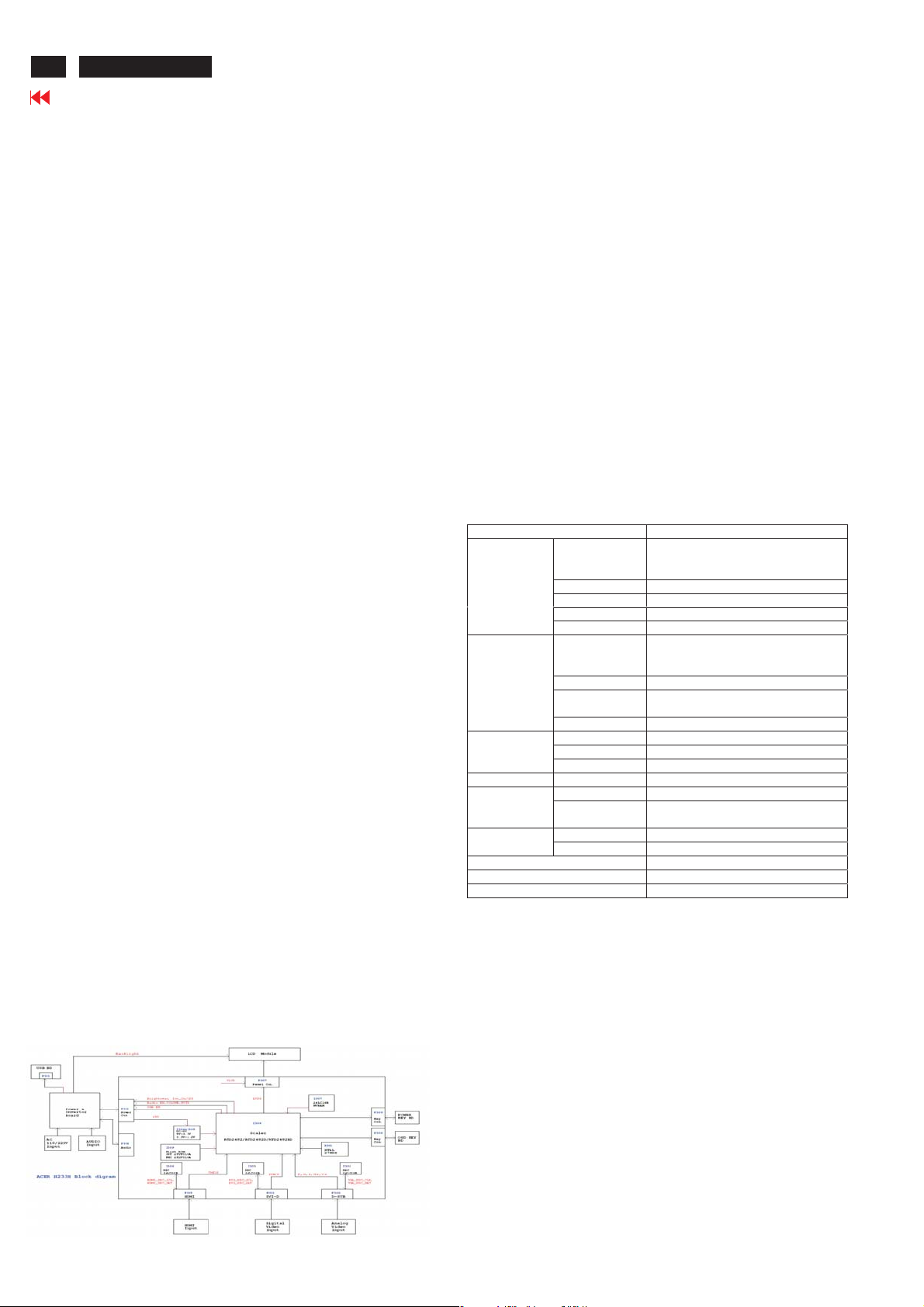
08. Block Diagram and schematic----------------------------------------------------------------------- 40
Appendix I : User s Manual
Appendix II User’s QSG
Appendix III :Spare Parts List
Appendix IV: Software Pack
------------------------------------------------------------------------------------- 12
’
aware of the necessary safety precautions to be used when serving electronic equipment containing
Published by Wistron Corporation Printed in Taiwan © All rights reserved Subject to modification
Safety Notice
Any person attempting to service this chassis must familarize with the chassis and be
high voltage.
26th-Nov.-2008
Page 2

Product Announcement:
Important Safety Notice
ACER H233H
Go to cover page
1
This product is certificated to meet RoHS Directive and
Lead-Free produced definition. Using approved critical
components only is recommended when the situation
to replace defective parts. Vender assumes no liability
express or implied, arising out of any unauthorized
modification of design or replacing non-RoHS parts.
Service providers assume all liability.
Qualified Repairability:
Proper service and repair is important to the safe,
reliable operation of all series products. The service
providers recommended by vender should being
aware of notices listed in this service manual in order
to minimize the risk of personal injury when perform
service procedures. Furthermore, the possible existed
improper repairing method may damage equipment or
Using Lead-Free solder to well mounted the parts.!
! The fusion point of Lead-Free solder requested in the
degree of 220 C.°
products. It is recommended that service engineers
should have repairing knowledge, experience, as well
as appropriate product training per new model before
performing the service procedures.
NOTICE:
!
To avoid electrical shocks, the products should be
connect to an authorized power cord, and turn off the
master power switch each time before removing the
AC power cord.
!
To prevent the product away from water or exploded
in extremely high humility environment.
!
To ensure the continued reliability of this product,
use only original manufacturer’s specified parts.
To ensure following safety repairing behavior, put the
!
replaced part on the components side of PWBA, not
solder side.
To ensure using a proper screwdriver, follow the
!
torque and force listed in assembly and disassembly
procedures to screw and unscrew screws.
Page 3
2
ACER H233H
Go to cover page
1. Product Specification
This model combine with three platform. See below
explanation.
1.Scaler IC:RTD2482D used in VGA ,DVI and HDMI port
Using simply word to define it(1A1D1H)
2.Scaler IC:RTD24823.used in VGA and HDMI port. Using
simply word to define it(1A1D)
Scaler IC:RTD2482RD used in VGA ,DVI and HDMI port
.Using simply word to define it.(1A1D1H+OD)
The product specification demonstrate all of the model:
1.1 SCOPE
This document defines the design and performance
requirements for a 23W inch diagonal , flat panel monitor .
The display element shall be a 1920x1080 resolution
TFT-LCD (Thin Film Transistor Liquid Crystal
Display).16.7M color(Hi-FRC) images are displayed on
the panel.Video input signals are analog RGB (0.7Vpp). When the system is powered-on , previously stored
screen parameters for a pre-defined mode will be
recalled if the operating mode is one of stored in
memory( 2213 factory timing mode).This monitor
operates normal by non-interlaced mode.
DDC (Display Data Channel) function is DDC2Bi
compliance. Power saving function complies with the
DPMS(Display Power Management Signaling)
standard.
1.2 GENERAL REQUIREMENTS
1.2.1Test Condition
Brightness level & contrast level max. Full white
pattern test mode following spec. Warm up more
than 1 hr, ambient light < 10 Lux , Luminance
meter CA210 or BM7 or same equipment
1.2.2Test Equipment
The reference signal source is a calibrated
Chroma 2237 video generator or higher. The use
of other signal generators during qualification and
production is acceptable provided the product
complies with this specification.
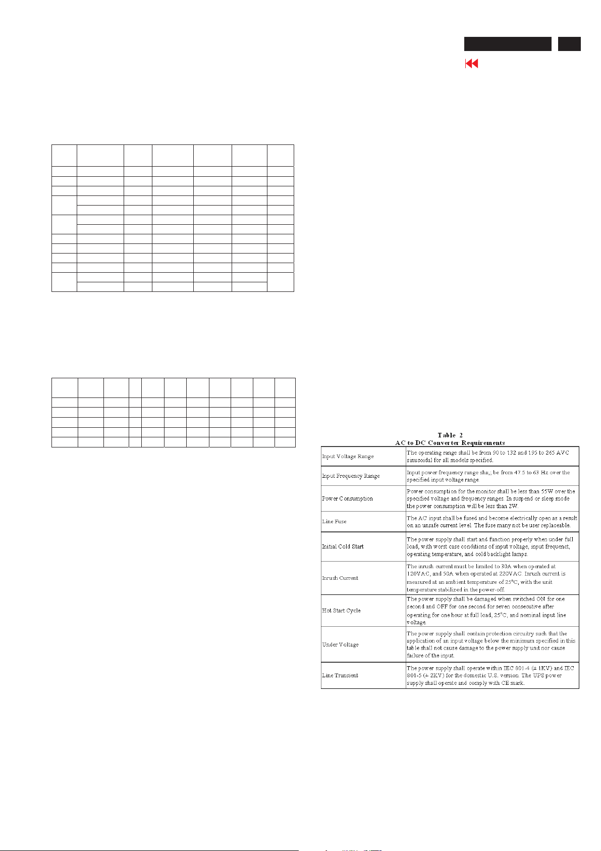
1.3 ELECTRICAL This section describes the electrical requirement of the monitor.
The LCD monitor consists of an interface board, a power board
and inverter board, a function key board.
The interface board will house the flat panel control
logic , brightness control logic, audio function control
(option), key function control, DDC and DC to DC
conversion to supply the appropriate power to the
whole board and LCD flat panel , and transmitting
LVDS signals into LCD flat panel module to drive the
LCD display circuit .
The power board will support main power DC5V to
interface board, and drive the two CCFLs (Cold
Cathode Fluorescent Tube).
The interface board provides the power ON / OFF
control over the power board.
Whole monitor to control the DPMS LED indicator to
function key board.
MONITOR SPECIFICATIONS
ITEM SPEC
Signal Input
(Analog)
Signal Input
(Digital)
Connector
Power Comsumption AC in 100V~240V Active 50W(non-USB)/60W(w/USB), power saving < 2W
Plug and Play VESA DDC2Bi
Power Saving VESA DPMS
InputSignalCounterTolerance
Frequency Analog:
Pixel clock 205MHz (Max)
Video Input Analog 0.7Vp-p
Display Pixels 640 x 480 (VGA) ~ 1920 x 1080
Sync Signal Separate SYNC for TTL (N or P)
Frequency Digital:
Pixel clock 165MHz (Max)
Video Input Analog 0.7Vp-p
Display Pixels 640 x 480 (VGA) ~ 1920 x 1080
AC Input
Input connector D-SUB 15 pin, DVI-D & HDMI
Audio Jack (OPTIONAL)
Front Input ,E-KEY,Auto Adjust ,Menu Adjust(-), A djust(+),Pow erUser’s Control
OSD Contrast, Brightne s s, Po sitio n , Clo c k , Pha se , Analog /D ig ita l,
Factory 13Pre-Defined Timing
User 9
H:31kHz~94kHz
V:50Hz~75Hz
H:31kHz~94kHz
V:50Hz~75Hz
Input Impedance 75Ω
AC100V ~ AC240V 10% 50/60Hz, 3 pin AC power cord
Audio input 3.6Φ
Reset, Color, Languag e se lec t, etc.
≦H 1kHz, ≦V 1Hz
1.3.1 Interface Connectors
1.3.1.1 Power Connector and Cables
The AC input shall have an IEC/CEE-22 type male
power receptacle for connection to mains power.
The power cord shall be with length of 1.8 0.005
meters.
1.3.1.2 Video Signal Connectors and Cable
The signal cable shall be 1.8 0.005 meters long.
At the end of the cable shall be a molded-over,
shielded, triple row, 15 position, D-subminiature
connector. The CPU connection shall have captive
screw locks, which will be adequate for hand
tightening. The monitor connection may use small
screws.
Page 4
1. Product Specification (continued)
ACER H233H
Go to cover page
3
Connector Pin Description
D-SUB Pin Description
Pin Name De scription
1 Red-V ideo Red video signal input.
2 Green-Video Green video signal input.
3 B lue - V id e o B lu e v id e o s ig n a l inp u t.
4GND Ground
5 DDC-GND DDC ground for the VESA DDC2Bifunction.
6 Red-G N D Analog signal ground for the R ed video.
7 Green-GN D Analog signal ground for the G reen video.
8 B lu e - G N D A n a lo g s ig n a l g r o u n d fo r th e B lu e v id e o .
9 +5 V +5V input from ho st system for the V ES A D DC 2 Bi function.
10 Sync - G N D Signal gro und
11 GN D Ground
12 DDC _SDA SDA signalinputfor the VES A D DCB2i function.
13 H - SY N C Ho rizontal signalinput from the ho st system.
14 V- S Y N C Vertical signal input from the ho st syste m.
15 DDC -SCL SCL signal inputfor the VESA DDC 2Bi function.
1.3.1.3 Audio Jack (option)
This jack shall connect the audio input from
host computer.
1.3.2 Video Input Signals
NO. Symbol Item Min Normal Max Unit Remark
1 Fh Scanning Horizontal Frequency 31 94 kHz Minimum Range
2 Fv Scanning Vertical Frequency 50 75 Hz Minimum Range
3 Vih Hi Level Input 2 5 Note 1)
4 Vil Low Level Input 0 0.8 V Note 1)
5 Video RGB Analog Video Level 0.0 0.7 1.0 V 75? to Ground
Note1) Schmitt-Triggers Input , Supported 3.3V device H ( & V) sync output from PC
1.3.2.1 Video Signal Amplitudes
The three video inputs consist of Red , Green ,
and Blue signals, each with its own coaxial cable
terminated at the monitor. These video signals are
analog levels, where 0 V corresponds to black ,
and 700 mV is the maximum signal amplitude for
the respective color, when each signal is
terminated by a nominal 75.0 ohms .For a given
monitor luminance levels are measured using this
defined video amplitude driving a monitor meeting
the termination requirements . The signal
amplitude is not to be readjusted to compensate
for variations in termination impendence.
1.3.2.2 Video Signal Termination Impedance
This analog video signal termination shall be 75
1% which shall be resistive with a negligible reactive
component.
1.3.2.3 Synchronization ( Sync ) Signals
The Horizontal Sync (HS) TTL signal is used to initiate
the display of a horizontal line. HS may be either active
high or active low, depending upon the timing .The
Vertical Sync (VS) TTL signal is used to initiate the
display of a new frame .VS may be either active high or
active low, depending on the timing .
1.3.2.4 Sync Signal Levels
The monitor must accept sync signals from both 3.3 and
5 volt TTL logic families.The inputs shall sense a logic 0
when the input is 0.8 volt or less and shall sense a logic
1 when the input is 2.0 volts or greater. In addition to
these level requirements , there shall also be a
minimum of 0.3 volt hysteresis provided for noise
immunity (typically by using a Schmitt Trigger input ).
That is , the input level at which the monitor actually
detects a logic 0 shall be at least 0.3 volt lower than the
level at which it actually detects a logic 1.If the monitor
sync processing circuits are designed around the 3.3
volt logic family ,then the sync inputs must be 5 volt
tolerant .
1.3.2.5 Sync Signal Loading
TTL input loading shall be equivalent to one TTL input
load. When logic 0 is asserted by a sync input , the
maximum current source from any single monitor sync
input to the driver is 1.6 mA .When logic 1 is asserted ,
the maximum current source from the driver to any
single monitor sync input is 400 uA .
1.3.2.6 Abnormal Signal Immunity
The monitor shall not be damaged by improper sync
timing , pulse duration , or absence of sync , or
abnormal input signal amplitude ( video and/ or sync too
large or too small) , or any other anomalous behavior of
a graphics card video generator when changing modes
, or when any combination of input signals is removed
or replaced . Additionally , under these conditions , the
monitor shall not cause damage to the driving source .
Ω
Page 5
4
ACER H233H
Go to cover page
1. Product Specification (continued)
1.3.3 User Controls and Indicators
1.3.3.1 Power On / Off Switch
The monitor shall have a power control switch
visible and accessible on the front of the monitor .
The switch shall be marked with icons per IEC 417
, # 5007 and # 5009.The switch shall interrupt the
DC supply to the monitor.
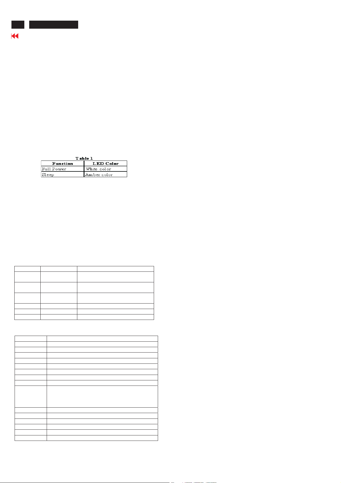
1.3.3.2 Power Indicator LED
The monitor shall make use of an LED type
indicator located on the front of the monitor .
The LED color shall indicate the power states as
given in Table 1.
1.3.3.3 On-Screen Display
The Wistron On Screen Display system shall be
used, controlled by a Menu button. If the buttons
remain untouched for OSD turn off time while
displaying a menu, the firmware shall save the
current adjustments and exit. Also, if the video
controller changes video mode while the OSD is
active, the current settings shall be save
immediately, the OSD turn off, and new video
mode is displayed.
Key WhenNoOSDdisplay OSDDisplay
MENU
Auto
Input Input source select Input source select
ITEM Content
Volume To increase or decrease the sound level
Brightness Adjust backlight luminance of the LCD panel
Contrast Adjust gain of R,G,B signal
Clock Adjust the ratio of dividing frequency of the dot clock
Focus Adjust the phase of the dot clock
H.Position The active screen is horizontally move right and left
V.Position The active screen is vertically move up and down
Color temp Select three kinds of modes(Warm, Cool, User)
OSD Language
OSD Position Adjust the OSD menu position
OSD Timeout The OSD menu show time
Setting The setting of Input Source, Wide Mode, DDC/CI
Information It will show resolution, the frequency of horizontal/vertical synchronizing and S/N
Reset All data copy from shipment factory data
Menu Display
Speaker Volume/Plus
>
(with Audio)
Speaker Volume/Minus
<
(with Audio)
Auto Adjust Function Menu exit
Trigger eColor Management Trigger eColor Management
e
1.USA-select the language among English, French, Italian, Deu tsch, Spanish, ,
,
2.EMEA-select the language among English, French,Italian, Deutsch, Spanish, Russian,
Dutch, Finnish
1.To select the OSD sub-Menu
2.Enter select
1.Right or Down selection of the OSD menu
2.Increase the value after bar selected
1.Left or up selection of the OSD menu
2. Decrease the value after bar selected
1.3.4 Monitor Modes and Timing Capability
1.3.4.1 Format and Timing
The monitor shall synchronize with any vertical
frequency from 50 to 75 Hz , and with any
horizontal frequency from 31 to 94KHz. If the input
frequency is out of the above – specified range,
the monitor shall display a warning screen
indicating that the input frequency is out of range.
Under no circumstances shall any combination of
input signals cause any damage to the monitor .
1.3.4.2 Factory Assigned Display Modes
There are 13 factory pre-set frequency video
modes. These modes have a factory pre-set
for all characteristics affecting front-of-screen
performance. When the system is powered
on, previously stored screen parameters for a
pre-defined mode will be recalled if the
operating mode is one of those stored in
memory. If the operating mode is not one of
those stored in memory, the monitor CPU will
select the PRESET timing for a mode that is
the next lowest in horizontal scanning
frequency to the mode being currently used.
The screen parameters may be adjusted by
the use of the front bezel controls and then
may be saved as a user defined mode. The
monitor shall include all the preset video
timings shown in the following page.( Please
see Note. (3) )
1.3.4.3 Mode Recognition Pull-in
The monitor shall recognize preset modes
within a range of 1KHz whichever is less for
horizontal ; and within 1Hz for vertical.
1.3.4.4 User Display Modes
In addition to the factory pre-set video modes,
provisions shall be made to store up to 9
user modes. If the current mode is a user
mode, the monitor shall select its previously
stored settings. If the user alters a setting, the
new setting will be stored in the same user
mode. The user modes are not affected by
the pre-set command. If the input signal
requires a new user mode, storage of the new
format is automatically performed during user
adjustment of the display (if required).( Please
see Note.(4) )
Page 6
1. Product Specification (continued)
PRESET PC TIMINGS (ANALOG AND DIGITAL
INPUTS)
Resolution
Mode
(active dot)
VGA 640x480@60Hz 800 x 525 31.469 59.941 25.175 4:3
MAC 640x480@66.66Hz 864x525 35 66.66 30.24 4:3
VESA 720x400@70Hz 900x449 31.469 70.087 28.322 1.8
800x600@56Hz 1024 x 625 35.156 56.250 36.000 4:3
SVGA
800x600@60Hz 1056 x 628 37.879 60.317 40.000 4:3
1024x768@60Hz 1344x8 06 48.363 60.004 65.000 4:3
XGA
1024x768@70Hz 1328x8 06 56.476 70.069 75.000 4:3
VESA 1152x864@75Hz 1600x900 67.5 75 108 4:3
SXGA 1280x1024@60Hz 168 8x1066 63.981 60.020 108.000 5:4
WXGA 1280x800@60Hz 1680x831 49. 702 59.810 83.500 16:10
WXGA+ 144 0x900@60Hz 1904x931 55.935 59.887 106.500 16:10
1920x1080@60Hz 2576x1120 67.158 59.963 173.000
HD
1920x1080@60Hz 2200x1125 67.500 60.000 148.500
Resolution
(total dot)
Horizontal
Frequency (KHz)
Vertical
Frequency (Hz)
Nominal Pixel
Clock (MHz)
PRESET VIDEO TIMING(DIGITAL INPUT)
CEA-861 H-Active V-Active I/P H-Total H-Back V-Total V-Back H-Freq. V-Freq. P-Freq.
-c-code Porch Porch (kHz) (Hz) (MHz)
1 640 480 p 800 48 525 33 31.5 60 25.2
2,3 720 480 p 858 60 525 30 31.5 60 27.027
4 1280 720 p 1650 220 750 20 45 60 74.25
5 1920 1080 i 2200 148 1125 15 33.75 60 74.25
16 1920 1080 p 2200 148 1125 36 67.5 60 148.5
Aspect
Ratio
16:9
ACER H233H
Go to cover page
1.3.5.3 Panel Timing and Interface
The controller supplied with the monitor shall
control all panel timing. This controller shall
adequately insulate the monitor from the computer,
so that no possible combination of input signals
from the computer shall cause damage to the flat
panel or any other component of the
monitor. The LCD panel interface shall support the
TFT standard.
1.3.6 DC - AC Inverter Requirements
The DC-AC inverter is on the power board. The
frequencies used by the DC-AC inverter used to power the
backlight shall be chosen so as to prevent any noticeable
effects on the flat panel (such as a rolling effect).
1.3.7 Power Supply Requirements
The AC to DC converter power supply for the monitor
shall be an external AC to DC converter ”brick” This brick
shall have an IEC receptacle for main power input and a
pin - in ---socket for DC power out. The brick shall provide
sufficient power for both the monitor and the backlight
assembly, and shall meet requirements specified in Table
2.
5
Analog input (VGA) treats all timings as PC-timings.
1.3.5 Controller Requirements
1.3.5.1 General Requirements
The monitor shall include a controller capable of
converting the analog RGB signal from a standard
1920x1080 resolution video controller in the CPU
to a signal which can be displayed on the panel.
The controller will include a PLL,A/D converters,
LVDS transmitter and other circuitry necessary to
perform its function. The PLL shall be stable
enough to ensure that a static image from the CPU
is placed in the same physical location on the flat
panel in each frame.
1.3.5.2 Video Stretching
The monitor shall contain provisions to “stretch”
the video signal, so that an input signal from the
computer in any resolution smaller than 1920 x
1080 is automatically expanded to fill the entire
screen.
Page 7

6
ACER H233H
Go to cover page
1. Product Specification (continued)
1.3.8 Display Communications Channel
The monitor assembly shall provide a display
communications channel that conforms to VESA
DDC2Bi hardware requirements. This configuration
shall contain the 128-byte (HDMI 256-byte)EDID file
as specified by VESA EDID standard. The monitor
should not write to the EDID file for the first two
minutes of operation following power-up UNLESS
some action taken by the user or the host CPU forces
the write (for instance, requesting the serial number
via the OSD). Furthermore, it is recommended that
CMOS switches be incorporated to isolate the DDC IC
from outside connections while the EDID Fault
Management is being updated. This is to prevent
corruption of the data by attempts to read the data
while it is being changed.
1.3.9 Firmware Update Function (same ISP function)
The update firmware need through from the D-Sub
connector, use DDC I2C bus to do update firmware.
1.4. ELECTRICAL
1.4.1 General Requirements
The panel used as the display device shall be an
1920x1080 resolution 23W, TFT LCD. This panel shall
be approved for use in this monitor.
1.4.2. Panel Timings
The controller included with the monitor shall translate
all video timings from the CPU that meet the timing
requirements listed in Panel specification into timings
appropriate for the panel. Under no circumstances
may the controller supply the panel with timings that
may result in damage . The controller shall insulate
the panel from the CPU , so that the panel shall
always be driven per it's own specification regardless
of the timings being sent from the CPU.
1.4.3.Polarizer Hardness
The outer face of the front polarizer panel shall be
covered with a coating witha#3hardness value .
1.4.4.Backlight Requirements
1.4.4.1 General Requirements
The backlight assembly shall be designed to
support field replacement at the customer site or
authorized service center.The lamps shall have a
continuous operating life of at least 50,000 hours
at 25 . The operating life is defined as having
℃
ended when the illumination of light has reached
50% of the initial value. The lamps shall extend a
sufficient amount from the edge of the light guide
that sputtering over the life of the lamps shall not
cause degradation of the luminance uniformity
(such as non-illuminated bands along the edges
of the display).
1.4.4.2 Lamps Startup Time
The backlight lamps shall start about 2 sec of the
time the monitor power switch is pressed or the
monitor is restarted from a power - down mode .
The starting time shall stay about 2 sec. for the
minimum expected life of the lamps.
Test conditions are as follows :
Ambient Light ---------------------- < 1.0 lux
Temperature-------------------------- 10
Inactive Time ----------------------- > 24 hours
1.4.5.Defects
1.4.5.1Visual Inspection
The LCD panel shall be inspected with all pixels
set to white, black, red , green , and blue. The
color variation, brightness variation , and overall
appearance must not be perceived as poor quality
.Areas and / or parameters considered
questionable shall be subjected to detailed
measurements .
1.4.5.2 Display Degradation
Over the life of the product , variation of the
parameters specified in Panel specification shall
be maintained within reasonable limits. The panel
must not exhibit any significant defects while in
operation ( excluding the CCFL operation ).This
does not in any way change the warranty given by
the panel manufacturer .
1.4.5.3 Light Leakage
Except for the active display area , there shall be
no light emission visible from any angle from any
other part of the display . For this test , the
ambient illumination must follow panel's
specification.
℃
Page 8
1. Product Specification (continued)
ACER H233H
Go to cover page
7
1.4.5.4 Allowable Defects
No cosmetic defects are allowed except those specified
below. The conditions of visual inspections are as
follows :
For 23 series
Viewing distance is to be approximately 35-50cm
Ambient illumination is to be 300 to 700 lux. Viewing
angle shall be at 90 degree. Defects not apparent within
one minute shall be ignored.
1.4.5.5 Defect Terminology
Table 3 gives the descriptive terms used in classifying
defects.
Spots or lines that appear dark in the display patterns and are
Dark / Spots / Lines
Bright Spots / Lines
Polarizer S cratch
Polarizer D ent
Rubbing Line
Newton R ing The “rainbow” effect caused by no n-uniform cell thickness.
M o ttling
Dim Line
Cross Lines Off
Bright / D ark D ot A sub – pixel (R,G,B dot) stuck off / on (electrical).
usually the result of contamination. D efects do not vary in
size or intensity (contrast) w hen contrast voltage is varied.
Contrast variation can be achieved through the use of varying
gray shade patterns.
Spots or lines that appear light in the display patterns.
Defects do not vary in size or intensity (contrast) w hen
contrast voltage is varied. C ontrast variation can be achieved
through the use of varying gray shade patterns.
W h e n the un it lig hts , lin es app e ar light (w hite ) w ith d isp lay
patterns dark and do not vary in size. Physical dam age to the
polarizer that does not dam age the glass
W hen the unit lights, spots appear light (white) w ith display
patterns dark and do not vary in size. Physical dam age to the
polarizer that does not dam age the glass.
Horizontal or diagonal lines that appear gray with the display
patterns dark and may have resulted from an “out of control”
rubbing process on the polyimide or “waves” on the B EFs or
prism sheets.
W hen the unit lights, variation / non – uniform ity
(splo tch in es s) app ea rs light (w hite ) w ith the dis pla y and
might vary in size.
W h e n the un it lig hts , lin e(s) in the m on ito r (v e rtical) or m ajo r
(horizontal) axis appear dim , but not completely on or off.
W hen the unit lights, lines in both the m inor and major axis
do not appear.
Average Diameter smaller of
(L+W)/ 2 or L/ 20+2W
Acceptable Number Minimum Separation
< 0.1mm Non countable N / A
0.1mm~0.3mm 10 15mm
0.31 mm ~ 0.5 mm 10 15 mm
0.51 mm ~ 1.25 mm 5 15 mm
1.26 mm ~ 2.5 mm 3 25.4 mm
2.51 mm ~ 3.75 mm 3 25.4 mm
Greater than 3.75 mm NONE Not applicable
Note : Allowable distance between spots of two sizes is the min imum separation
number for the smaller spot. Therefore, if there are two spots, 1.30mm and 0.4mm
in diameter, they must be at l east 15mm ap art.
1.5 Optical Characteristics Depends on the LCD supplier's spec. Details refer to QA Inspection Spec.
1.4.5.6 Smudges, Streaks and Smears
When viewing the panel oriented so as to maximize
reflected light , there shall be no visible smudging ,
streaking, smearing or other non-uniformity from
contaminants ,fingerprints, or defects in any of the visible
surfaces. This is independent of whether the unit is
operating or off .
1.4.5.7 Other Defects
Undefined defects that are considered to be rejectable
will be reviewed as they become apparent. These
panels will be referred to the Corporate / Manufacturer
Purchasing Agreement for disposition.
1.4.5.8 LCD Inspection
Put LCD panel on inspection table and illuminate the
panel with a daylight fluorescent lamp located above
the panel surface such that the luminance at the LCD
panel is between 1000 lux and 1500 lux .Defect limits
are given in Table 4 .
Table 4
Page 9
8
ACER H233H
Go to cover page
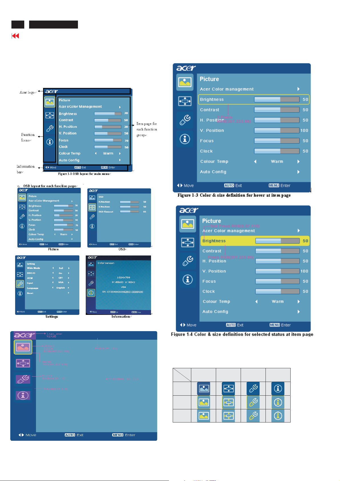
2 OSD Menu
2.1 MAIN OSD MENU a. Display OSD menu when user press “MENU” button on
front bezel
b. Layout as following figure 1-1
The description for control function
d. The definition of size and color for main menu
Figure 1-2 color & size definition for function Icons
e Icons instruction
Function
Stat us
Non-Focus
Focus
Focus on
Item-page
Picture OSD Setup Information
Page 10
2. OSD Manu (continued)
ACER H233H
Go to cover page
9
f. Item page status
Status Display type
Non-focus
Item focused
Item selected
The description for control function
Key Function description
Power Power off the monitor
<Movingthefocusup
>Movingthefocusdown
Menu
Auto Exit the OSD menu
e Trigger the acer eColor Management
Key Function description
Power Power off the monitor
<Movingthefocusup
>Movingthefocusdown
Menu Select function item for adjustment
Auto Exit from the item page to icon place
e Trigger the acer eColor Management
Enter to the item page
1. It has no function at the information
page.
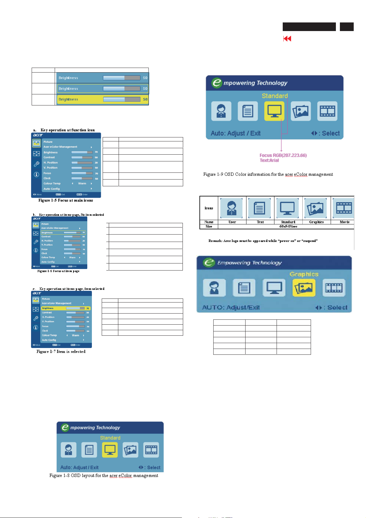
c. The definition of color & size for the acer eColor management
OSD
d. Icons introduction
Scenario mode:
Key Function description
Power Power off the monitor
< Decrease the setting value for target item
> Increase the setting value for target item
Menu No function
Auto Exit from item selected status
e Trigger the acer eColor Management
Acer eColor management
a. Display acer eColor Management OSD when user press
“e” button on the front bezel or trigger this function in OSD
menu/picture page.
b. Layout as following figure 1-8
Mode Contrast (OSD) Brightness (OSD)
User mode (User defined) (User defined)
Text mode 50 (slope 1.0) 44 (61%)
Standard mode 50 (slope 1.0) 77 (85%)
Graphics mode 60 (slope 1.04) 97 (98%)
Movie mode 56 (slope 1.025) 77 (85%)
Note: The contrast/brightness value of modes should be
adjusted by requirement.
Operation method:
Step 1: Press “e” key to initial scenario mode.
Step 2: Press “>” or “<” key to select the mode you want (not
cyclic).
Step 3: If user has NO action after Step 2, OSD will disappear
after 10 sec and do “auto scan” (mode keep in original
one, no change).
If user press “e” key after Step 2, it means user confirm
the chosen mode and monitor will do “auto scan” as
well.
Page 11
10
ACER H233H
Go to cover page
2. OSD Manu (continued)
Volume management OSD
a. Display volume management OSD, when user press “<” or “>”
button on front bezel.
b. Layout as following figure 1-10, key operation at items page
(No item selected)
Key Function description
Menu
Auto
input
Close volume OSD
e
< Volume down
>Volumeup
c. The definition of color & size for the volume management
OSD and file
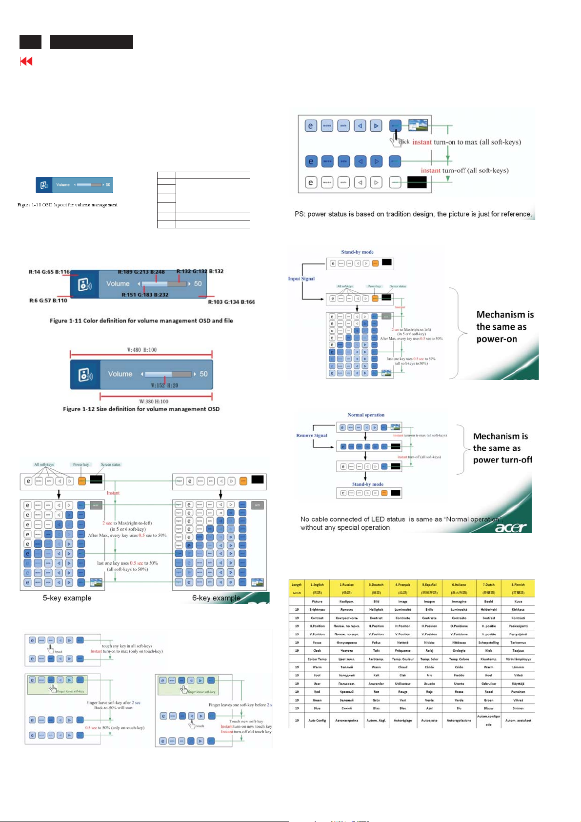
Power turn-off
Stand-by then Input Signal
LED Light Effect in Soft-key
Power ON
Normal operation
Normal Operation then remove Signal
Appendix
*Multiple language
Page 12
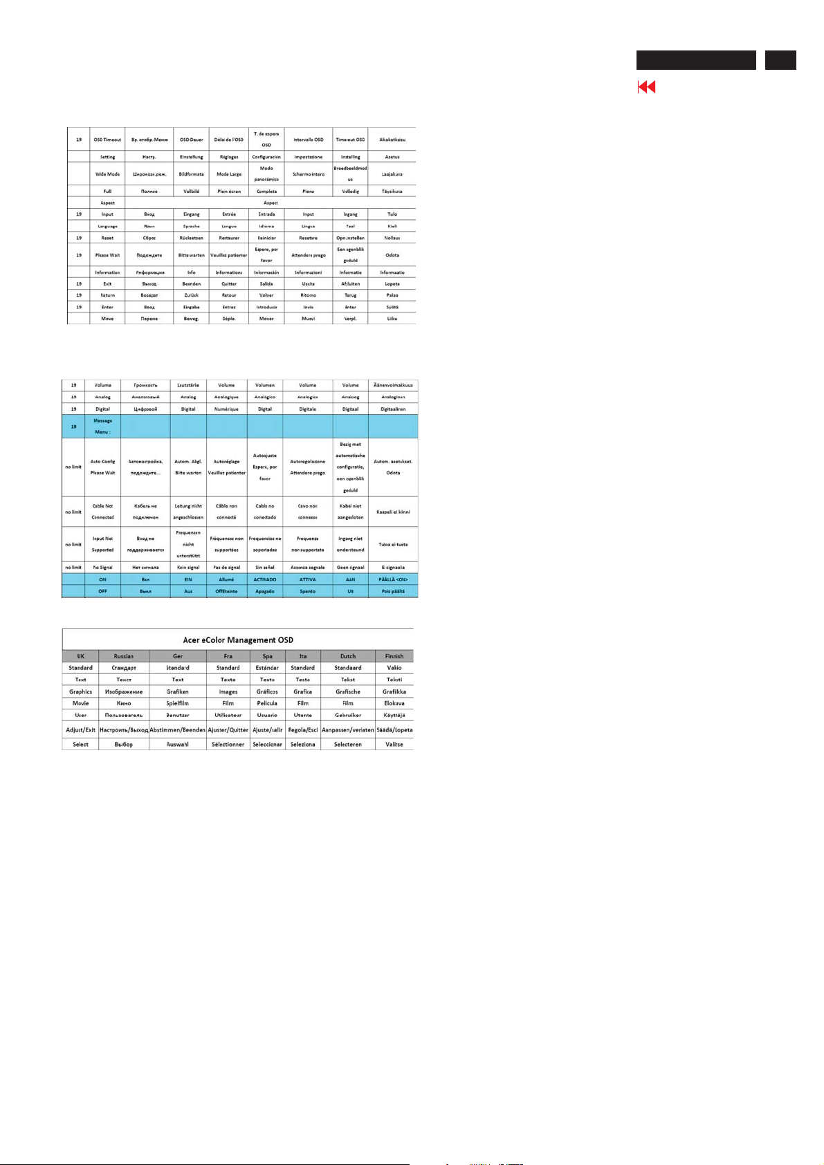
2. OSD Manu (continued)
ACER H233H
Go to cover page
11
Page 13
12
ACER H233H
Go to cover page
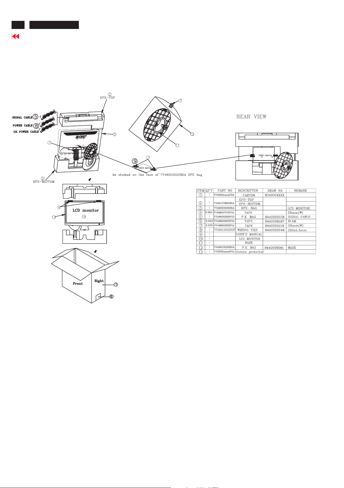
3.1 Packing Exploded Diagram
3. Exploded Diagram
Page 14
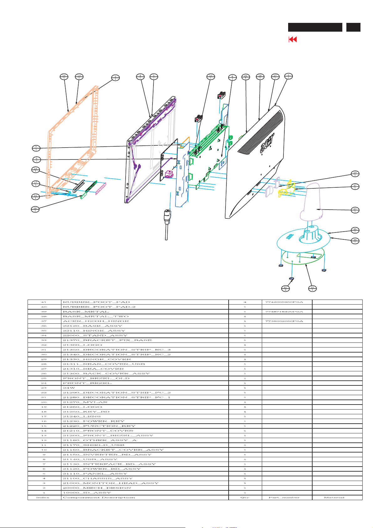
3.2 Product Exploded Diagram
3. Exploded Diagram (continued)
ACER H233H
Go to cover page
13
Page 15
14
ACER H233H
Go to cover page
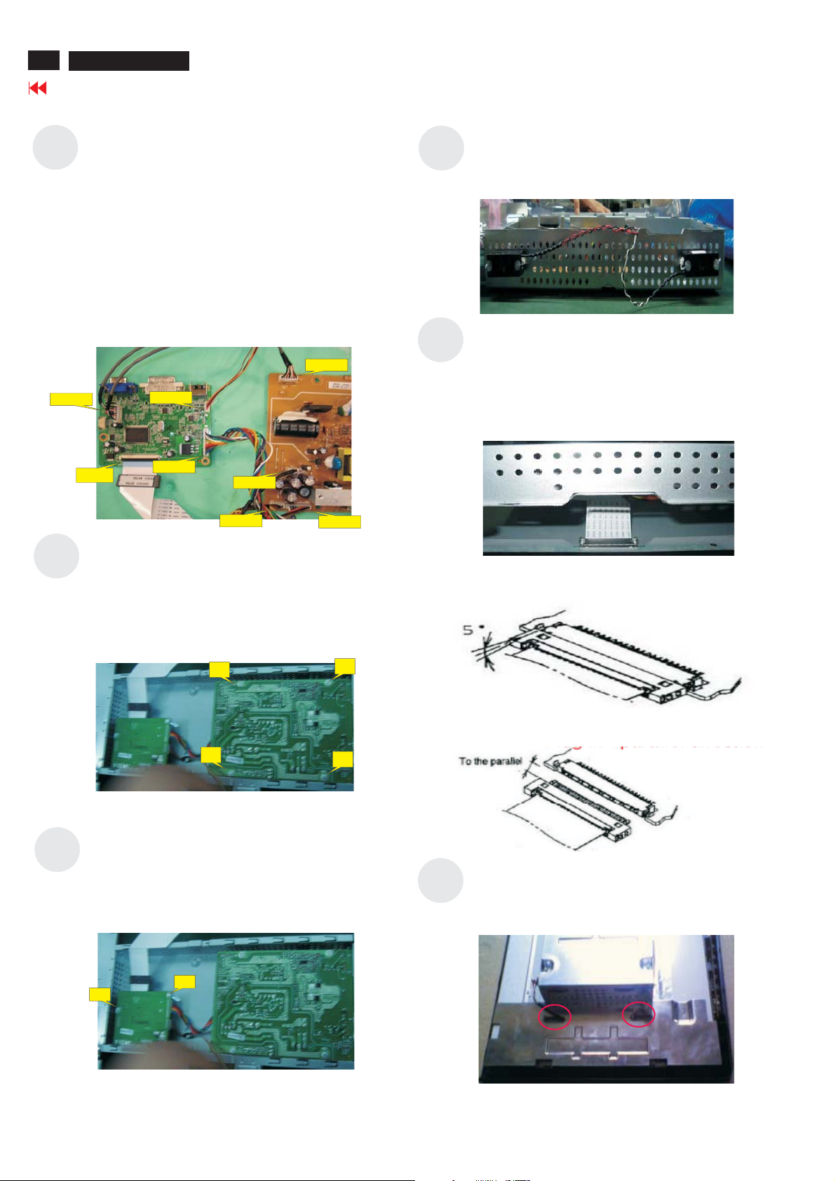
4.1 Assembly procedures:
Connect the cable between power board(P802)
S1
P308
and interface board (P301)
Connect the cable between power board(P003) and
interface board(P308)
Connect the USB board cable(P301) into interface
board(P805)
Connect speak cable into interface board(P001)
Connect the FFC cable into interface board
Connect the power key cable(P601)into interface
board(P309)
P309
4. Assembly and Disassembly Procedures
Fix the speaker and speaker cable, The white line
S4
S5
P003
intheleft,theredlineintheright.
Turn the monitor faced down and put it on the
bracket chassis module till both parts firmly
Connect FFC cable to LCD panel. There are
two locks over here when plugging in should be
noticed.
S2
S3
FFC
Use a Phillips-head screwdriver screwed the
No.1~4 screws till that power board and bracket
chassis base firmly attached.(No1~3 screw
size=M3x6; No4 screw size=M4x8;
Torque=9~10KGFxCM).
Use a Phillips-head screwdriver screwed the
No.1~2 screws till that interface board and bracket
chassis base firmly attached.
(No1~2 screw size=M3x6; Torque=9~10KGFxCM).
P301
P001
P805
1
3
P802
2
4
S6
Plug in parallel direction
Angel < 5 degrees
Take lamp cables out from the holes shown as the
photo.
2
1
Page 16
4. Assembly and Disassembly Procedures (continued)
ACER H233H
Go to cover page
15
S7
S8
Plug 2 lamp cables to the connectors of inverter
board.
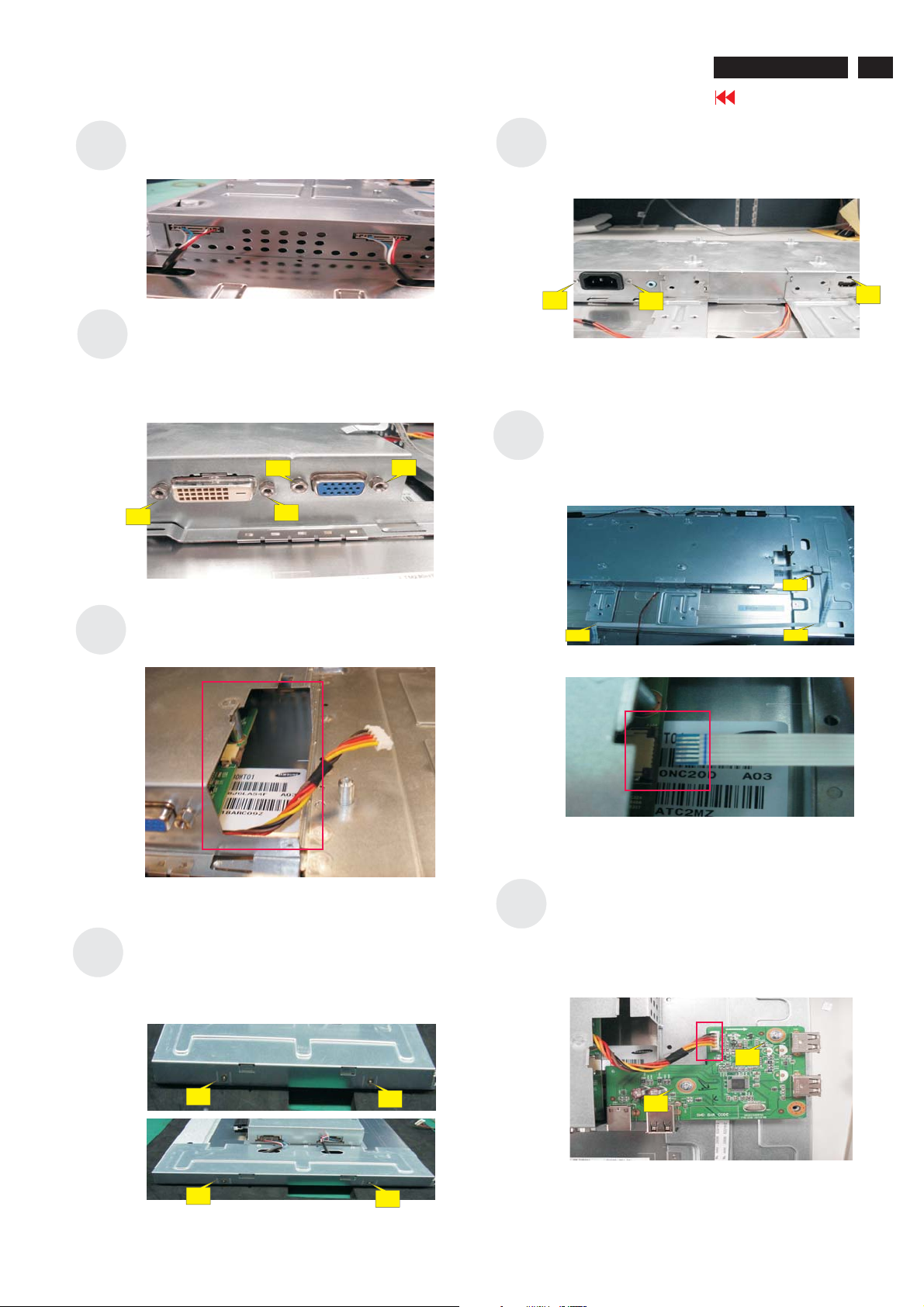
Use a Hex-head screwdriver screwed the DVI and
D-SUB connectors (No.1~4 Hex Nut screws
Size=M3x8;Torque=4~6KGFxCM).
2
4
3
1
S11
S12
Use a Phillips-head screwdriver screw 3 screws
(No1~2 Screw Size=M3x10;No3 screw size=M3*6
Torque=4~6KGFxCM).
2
Stick the safety tape
Connect OSD key cable into interface board(P306)
1
3
S9
S10
Take out the USB cable to through out the hole.
Use a Phillips-head screwdriver screw 4 screws
(No1~4 Screw Size=M3x6;
Torque=2.5~3KGFxCM).
S13
1
3
Use a Phillips-head screwdriver screwed the
No.1~2(No1~2 screw size=M3x6; Torque=9~10
KGFxCM).
Connect the USB cable.
2
1
2
4
1
3
2
Page 17

16
ACER H233H
Go to cover page
4. Assembly and Disassembly Procedures
S14
S15
Use a Phillips-head screwdriver screwed the
No.1(No1screw size=M3x4; Torque=5+/-1
KGFxCM).
1
Connect the power key cable.
Connect the power key board from front bezel,
Use a Phillips-head screwdriver screwed the
No.1~2 screws(No1~2 screw size=M2x3.3;
Torque=1~1.5 KGFxCM).
S17
S18
Stick the power key cable with tape.
rc ota ua
Put a ear over n he ssembled nit nd
ress on force echanisms ocked nd irmly
pmlaf
attached
.
S16
1
Fix with the OSD key board on the front bezel
2
S19
4
3
2
1
Use a Phillips-head screwdriver screw 1 screw
(No1 Screw Size=M3x10;
Torque=7.5~9.5KGFxCM).
4
3
2
1
1
Page 18

ACER H233H
Go to cover page
17
S20
S21
Assemble the stand upper side to the rear cover
through the way of screwing 4 screws till both
units firmly attached.
(No1~4 Screw Size=M4x10;
KGFxCM).
2
3
Assemble the hinge cover into both two sides.
Torque=12+/-
1
4
S23
Stick POP label on the correct position the same
as below photo
S22
Stick a screen card on the front bezel with two
tapes.
S24
S25
Take a LDPE+EPE bag to cover the LCD
monitor.
Take two cushion foams; one is held the top side
of LCD monitor, and another is held the bottom
side.
Page 19

18
ACER H233H
Go to cover page
Put accessories of stand, DVI cable, and
S26
S27
user’s manual ,power cable on specific
positions as photo below.
Move previous assembled parts into the carton
then stick Vista and feature label on the carton
then packing the carton
4. Assembly and Disassembly Procedures (continued)
Page 20

4.2 Disassembly procedures
Open the carton with a proper tool.
S1
Take out all accessories including D-SUB
S2
cable power cable, DVI cables, user’s
manual, and packing material from the carton.
(Note: It depends on whether users
returning the accessories.)
4. Assembly and Disassembly Procedures (continued)
FEATURE LABEL
VISTA LABEL
S4
ACER H233H
Go to cover page
P
ut returned unit on a protective cushion,then
remove LDPE+EPE bag.
Tear off tapes to remove the screen protector
card then turn over the LCD monitor (screen
faced down),
19
S3
Take off two cushion foams
S5
S6
Disassemble the stand cover.
Use a Phillips-head screwdriver unscrew 4 screws
to release the stand base.
(No1~4 Screw Size=M4x10;
Torque=12 KGFxCM).±1
2
3
1
4
S7
Use a Phillips-head screwdriver unscrew 1 screw
(No1 Screw Size=M3x10;
Torque=7.5~9.5KGFxCM).
1
Page 21

20
ACER H233H
Go to cover page
4. Assembly and Disassembly Procedures (continued)
S8
S9
Put the dissembled monitor closed to by myself
RIGHT SIDE
UP SIDE
LEFT SIDE
Turn over the LCD monitor (screen faced up).
DOWN SIDE
S12
Separating all of the locking mechanism of the
front bezel in turn.
S10
S11
edge your finger between the front bezel and
W
the panel, then pry up on the front bezel to
disengage the locking mechanism.
Note: The dissemble method of front bezel is
as the below photos description, although the
photos from S9 to S13 are not suitable for this
model.
Insert steel rule between panel and front bezel
.Using properly force to let the locking
mechanism of front bezel and rear cover
separated
S13
Hold the one upside corner of the front bezel after
separating the upside of the front bezel
Using properly force to pull up front bezel that
will let the locking mechanism of left side, right
side and down side separated.
Page 22

4. Assembly and Disassembly Procedures (continued)
ACER H233H
Go to cover page
21
S14
Hold one side of down side that had been
separated from front bezel
Use properly force to pull up front bezel
S17
S18
Use a Phillips-head screwdriver unscrewed the
No.1(No1screw size=M3x4; Torque=5+/-1
KGFxCM).
1
Use a Phillips-head screwdriver unscrewed the
No.1~2(No1~2screw size=M3x6; Torque=9~10
KGFxCM).
Unplug the USB cable and OSD key cable.
1
2
S15
Use a Phillips-head screwdriver unscrewed the
No.1~2 screws(No1~2 screw size=M2x3.3;
Torque=1~1.5 KGFxCM).
Unhook the power key board from front bezel,
disconnect the power key cable.
1
Tear off shield safety tape
Disconnect the OSD key cable
2
S19
S20
Use a Hex-head screwdriver unscrewed 4 screws to
release the DVI and D-SUB connectors
(No1~4Hex Nut screws
Size=M3x8;Torque=4~6KGFxCM).
2
4
Use a Phillips-head screwdriver unscrewed the
No.1~3 screws to release the power connector and
HDMI connector.
(No1~2 screw size=M3x10; No 3 screw size=M3x6
Torque=4~6 KGFxCM).
3
1
1
3
2
2
1
3
Page 23

22
ACER H233H
Go to cover page
4. Assembly and Disassembly Procedures (continued)
S21
S22
Use a Phillips-head screwdriver unscrewed the
No.1~4 screws
(No1~4 screw size=M3x5; Torque=2.5~3 KGFxCM).
2
4
Disconnect the lamps cable
Take out lamp cables right through the No.1-2
square holes and separate the bracket chassis
module and LCD panel apart.
1
3
S25
S26
Examine the panel surface accoring to inspection
criteria. Put it aside.
Use a Phillips-head screwdriver unscrewed the
No.1~2 screws to release the interface board.
(No1~2 screw size=M3x6; Torque=9~10KGFxCM).
2
1
S23
S24
1
Use long nose pliers to separate plastic hook
Disconnect the FFC cable to the connector of
panel.
Use finger to push the lock according to arrow
direction then take out the FFC cable
2
S27
S28
P308
Use a Phillips-head screwdriver unscrewed the
No.1~4 screws to disassemble the power board.
(No 1~3 screw size=M3x6; No 4 screw
size=M4x8; Torque=9~10KGFxCM).
1
3
Disconnect all of the cable
P309
2
4
P003
FFC
P301
P001
P805
P802
Page 24

5. Troubleshooting
5.1 No display of screen Screen is black color of LED is amber.. ( , )
Does OSM display when you push
“MENU key.
ACER H233H
Go to cover page
23
When a signal isn't being inputted, it is
indicated with "No Signal Input". it is
indicated with "Out Of Range" at the time
of the frequency that it can't be
distinguished.
Check if the sync signal from computer is
output and if the video cable is connected
Proceed "checking the resolution change IC
Yes
normally.
OK
movement" section.
No Proceed "No OSM display" section.
NG
Input the sync signal of computer, or change
the cable.
Page 25

24
ACER H233H
5. Troubleshooting (continued)
Go to cover page
5.2 Nothing display on screen (screen is black, color of LED is blue)
Is backlight lit?
OK
Does computer output RGB video signals?
OK
Check OSM menu is display on screen
when you push the "MENU" key.
OK
NG
NG
NG
Refer "Checking the backlight unit" section"
Check the video cable for failure. Check the host for output signal is all
black or not.
1) Change pattern of video signal output on the host.
2) Reconnect the video cable.
3) Change the video cable.
Check if the LCD video signal cable is connected between the Interface
Board and LCD module.
Proceed "Abnormal sreen" dection"
OK
Next Page
NG
Failure Point
The LCD video signal cable is disconnected.
Page 26

5. Troubleshooting (continued)
5.2 Nothing display on screen (screen is black, color of LED is blue)continued
Continue
Check the 5V power supply for
P301 pin 4,5,6.
NG
ACER H233H
Go to cover page
25
OK
Check the I304 pin2 if
voltage is 3.3V
OK
Check the I305 pin2 if
voltage is 1.2V
OK
Check the I301 pin2 if
voltage is 5V
OK
Check if the voltage
between I301 pin2 and
pin3 is above -0.7V
OK
Failure Point
I301 is failure.
NG
NG
NG
Proceed "Checking the DC/D C converter
Proceed "Checking the DC/D C converter
Failure Point
1) FB301 is open..
circuit" section.
circuit" section.
Check the input voltage level whether was changed when
pressed function keys on the P309 pin1
OK
Check the P307 all LVDS signals.
Failure Point
NG
OK
Failure Point
1) The LVDS cable broke between P307
and LCD module.
2) LCD module is failure.
1) Printed wire broke between P307 and
2) I308 is failure.
NG
I308 LVDS signals.
Check if the voltage on I308 pin 108 that is
Failure Point
I308 is failure
from 3.3V to 0V.
OK
NG
Failure Point
1) Printed wire broke between P309 pin 1
and I308 pin 108.
Page 27

26
ACER H233H
Go to cover page
5.3 Checking the back light unit
Is +22V supplied to inverter PWB ? (by the
5. Troubleshooting (continued)
power board)
Failure Point
OK
NG
Check the BKLT_EN signal of the DC input
P301 pin 2 at TTL high level.
NG
OK
Check the BKLT_ADJ signal of the input
P301 pin3 from I308 pin102 is a PWM
signal.
1) Power board of Inverter part failure.
Failure Point
1) printed wire broke between P301 pin2,
R304 and I308 pin 101.
2) I308 is failure.
Failure Point
OK
NG
Failure Point
1) Back light unit of LCD module is failure.
2) Inverter Cable disconnect
1) printed wire broke between P301 pin3,
R501 and I308 pin102.
Page 28

5.4 Abnormal screen for VGA
Check the R, G, B video signal from computer
5. Troubleshooting (continued)
input on P302 of D-sub connector.
ACER H233H
Go to cover page
27
NG
OK
Check the R, G, B input video signals on I308
pin25, 27, 30 respectively that their level is 0.0 to
0.7Vp-p.
NG
OK
Check all LVDS signals being output to P307
from I308?
NG
OK
Failure Point
1) No R, G, B video signals output from host
computer, check computer.
2) Video signal cable disconnection.
Failure Point
In the case of the Red signal. (A Green and Blue
signal is the same path, too.)
1) Printed wire broke between P302 pin1 and
I308 pin30.
2) Video cable is failure.
3) FB315,FB306,R327,C315 is open.
4) R326,C329 is short or open.
Failure Point
Printed wire broke between I308 and P307.
Proceed "Checking the resolution change IC
movement" section.
Page 29

28
ACER H233H
5. Troubleshooting (continued)
Go to cover page
5.5 Abnormal screen (For DVI and the same for HDMI)
Check the DVI video signal from computer input
on P303 of DVI connector.
NG
OK
Check the DVI input video signals on I308 pin
12,13,14,15,16,17,18,19 respectively that
differential input voltage is 150 to 1200mV, and
input commond mode voltage is 3.3V.
NG
OK
Check all LVDS signals being output to P307
from I308?
NG
OK
Failure Point
1) No DVI video signals output from host
computer, check computer.
2) DVI Video signal cable disconnection.
Failure Point
In the case of the DVI_RX0+/- signal. (A
DVI_RX1+/-, DVI_RX2+/- and DVI_RXC+/signal is the same path, too.)
1)Printed wire broke between P303 pin 17, 18 and
I308 pin 12. 13.
2) Video cable is failure.
3) R350, R355 open.
Failure Point
Printed wire broke between I308 and P303.
Proceed "Checking the resolution change IC
movement" section.
Page 30

5.6 Abnormal OSM display adjust problem
5. Troubleshooting (continued)
ACER H233H
Go to cover page
29
Check the input I2C signal whether is changed when pressed
function keys on the P306 pin 4, 5
OK
Check the input I2C signal of I308 pin 50, 51 whether is
changed when pressed function keys.
OK
NG
NG
Failure Point
1) Function key wire disconnection.
2) Function key wire is failure.
3) Function key board is failure.
Failure Point
1) Printed wire broke among P306 pin4, R368 and I308 pin51
2) Printed wire broke among P306 pin5 ,R362 and I308 pin50
3) C393, C394 is short.
4) D352, D353 is short
Failure Point
I308 is failure.
Page 31

30
ACER H233H
Go to cover page
5.7 Abnormal plug and play operation for VGA
Confirm the host computer supplies DDC2B mode.
5. Troubleshooting (continued)
NG
OK
Check the voltage on P302 pin 9 that is power DC 5 V.
NG
OK
Check the signal on P302 pin12, 15 that is serial data
/ clock signal.
NG
OK
Failure Point
The host machine is not communicatiog in DDC2B mode.
Failure Point
TheVideo cable is failure.
Failure Point
The Video cable is failure.
Check the output signal of serial data / clock on I308
Failure Point
1) Printed wire broke among I308
pin58,59,R429,R434,R320,R321 and P302 pin12,15
2) I308 maybe failure.
3) R314 ,R315 is open.
4) D306 or D308 or C320 or C321 is shorted.
pin 59, 58.
OK
NG
Failure Point
I308 is failure.
Page 32

5. Troubleshooting (continued)
5.8 Abnormal plug and play operation (For DVI and the same for HDMI)
Confirm the host computersupplies DDC2B mode.
Failure Point
NG
OK
Check the voltage on P303 pin14 that is power DC 5 V.
The host machine is not communicatiog in DDC2B
mode.
ACER H233H
Go to cover page
31
NG
OK
Check the voltage on P303 pin 16 that is 4.5V.
NG
OK
Check the voltage on P303 pin 7, 6 that is serial data /
Check the output signal of serial data / clock on I308
clock signal.
OK
pin 122,121
NG
Failure Point
The Video cable is failure.
Failure Point
1) Printed wire broke between P303 pin 14 and pin 16.
Failure Point
The Video cable is failure.
OK
Failure Point
1) Printed wire broke between I308 pin121, 122,
,R410, R414, R344, R345 and P303 pin7,6
2) I308 maybe failure.
3) R338, R339 is open.
4) D320 or D321 or C339 or C342 is shorted.
NG
Failure Point
I308 is failure.
Page 33

32
ACER H233H
5. Troubleshooting (continued)
Go to cover page
5.9 Checking the interface circuit of sync signal
5.9.1 Checking the control circuit of horizontal sync pulse
Check the horizontal sync signal on P302 pin13 TTL
level.
NG
OK
Check the horizontal sync signal on I308 pin 22 TTL
level.
NG
OK
Failure Point
Proceed "Checking the resolution change IC movement"
section.
5.9.2 Checking the control circuit of vertical sync pulse
Failure Point
Video cable is failure.
Failure Point
1) Printed wire broke between P302 pin13 and
I308 pin22.
2) FB304 , R405 is open.
3) D307 ,R319 or C322 is short.
Check the vertical sync signal on P302 pin14 TTL level.
NG
OK
Check the horizontal sync signal on I308 pin21 TTL
level.
NG
OK
Failure Point
Proceed "Checking the resolution change IC movement"
section.
Failure Point
Video cable is failure.
Failure Point
1) Printed wire broke between P302 pin14 and
I308 pin21.
2) FB305 or R331 is open.
3) D310,R318 or C313 is short.
Page 34

5. Troubleshooting (continued)
5.10 Checking the resolution change IC movement
Check +3.3V supply on I304 pin2.
ACER H233H
Go to cover page
33
OK
Check +1.2V supply on I305 pin 2.
OK
Check X301 27MHz clock input to I308 pin 127 and 128 at TTL level.
OK
NG Proceed " Checking the DC/DC converter circuit" section.
NG Proceed " Checking the DC/DC converter circuit" section.
NG
Failure Point
1) Printed wire broke between X301 and I308 pin 127, 128.
2) C351, C352 is short or open.
3) R507 is open.
4) X301 failure.
Check I308 pin 125 RSTB signal is high level at normal operation.
OK
Check I308 pin 115,116,117,118
Failure Point
I308 failure.
SPI signal.
OK
NG
Failure Point
1) Printer wire broke between I308 pin 125 and
R437
NG
Failure Point
1) Printed wire broke between I308 pin 115, 116, 117,118 and I309 pin 1,2,
5,6.
2) I309 is failure.
3) I308 is failure.
Page 35

34
ACER H233H
Go to cover page
5.11 Checking the DC/DC converter circuit
Check the 5V is output from P301 pin 4,5,6.
5. Troubleshooting (continued)
NG
OK
Check the 5V is input to I304 pin3.
NG
OK
Check the 3.3V is output from I304 pin2, 4.
NG
OK
Check the 3.3V is input to I305 pin3.
NG
OK
Failure Point
1) Power wire disconnection.
2) Power board is failure.
Failure Point
1) Printed wire broke between P301 pin 4,5,6
and I304 pin3.
Failure Point
1) I304 is failure
2) C306 or C308 short.
Failure Point
1) Printed wire broke between I304 pin2. 4 and
I305 pin3.
Check the 1.2V is output from I305 pin2,4.
NG
OK
Failure Point
1) FB311 or FB312 or FB319 or FB320 is open.
Failure Point
1) I305 is failure
2) C310 or C311 short.
Page 36

6. Firmware Upgrade Process
ACER H233H
Go to cover page
35
6.1 Hardware Configuration
Connect VGA
cable between
monitor and kit
Connect USB
and VGA
cable between
PC and kit
6.2 Realtek F/W Configuration:
Step-1 Launch the utility of “ ”DebugTool_V6.2.exe
If it shows “No USB Device”, there is a problems with
communication .you should confirm your USB device
whether be detected by your PC device management or
reconnect the USB cable again.
Step-3Select ISP type: Serial Flash
Select ISP icon.
Step-2 Select “USB”
Step-4 Follow up the red square indication
Select P-flash and Auto
Page 37

36
ACER H233H
Go to cover page
6. Firmware Upgrade Process (continued)
Step-5 Select “64K” icon to load firmware image. There are two
HEX files. You only need to select “64K” to choose
“H233H_EMEA.H00.hex” and
“H233H_EMEA.H01.hex” will be loaded
in “64~96” automatically.
Step-6Press button
Check firmware version
Turn off the power,then press force on “ POWER ” and “ E ”
button at the same time then press on “ MENU ”button to
enter factory mode
Note: Please pay attention ,Don’t change any parameter
which is measured by precise machine before shipping out
The screen will show “PASS”
Page 38

7. Writing EDID Process
ACER H233H
Go to cover page
37
Hardware Configuration:
1. Connect the PRINTER PLUG of DDC FIXTURE with the
printer port of Desktop PC.
2. Plug USB A PLUG of DDC FIXTURE to USB socket of
Desktop PC
3 Use DVI cable connect to the DVI socket of monitor
of DDC FIXTURE.
4 Take a video cable then connect the D-SUB PLUG and the
D-sub socket of monitor.
5. Re-confirm all the connectors are connected well.
PARALLEL CONNECTION
USB CONNECTION
DVI CONNECTION
Writing EDID for VGA and DVI
S1 Chose the folder:” X233H-H233H-VGA&DVI “
Double click “ Acer_1A1D_RLT.EXE “
S2 Select Model: Key in password”cedid” then select
model which one you want to write EDID code that it
depends on panel type.
VGA CONNECTION
S1 Open EDID Write protection function
Turn off the power,then press force on “ POWER ” and “ E
” button at the same time then press on “ MENU ”button to
enter factory mode.
Select “EDID WP” to let it be off.
Note: Please pay attention ,Don’t change any parameter
which is measured by precise machine before shipping
out.
cedid
SS:MEANS SAMSUNG PANEL
Page 39

38
ACER H233H
Go to cover page
7. Writing EDID Process (continued)
S3 Choose "WRITE" from menu then select "Scan S/N
And Write EDID And Test DDC”
S4 Key in series number in the input column and input 2
column
Press write button after key in S/N
Hardware Configuration:(Writing EDID for )
HDMI port’s
1. Connect the PRINTER PLUG of DDC FIXTURE with the
printer port of Desktop PC.
2. Plug USB A PLUG of DDC FIXTURE to USB socket of
Desktop PC
3 Use DVI transfer HDMI cable connect between of the DVI
EXTENDING SOCKET and Monitor(Writing EDID for HDMI
port)
4 Take a video cable then connect the D-SUB PLUG and the
D-sub socket of monitor.
5. Re-confirm all the connectors are connected well.
PARALLEL CONNECTION
USB CONNECTION
VGA CONNECTION
S5 When EDID was written successfully that will show below
message on the screen
HDMI TRANSFER DVI CONNECTION
Entering Factory mole to let “EDID WP” be off
Writing EDID procedure
S1 Choose the folder “X233H-H233H-HDMI”
Double click “ AcerHDMI_RLT “
The writing process same as writing VGA and DVI
process.
Page 40

7. Writing EDID Process
ACER H233H
Go to cover page
39
S5 When EDID was written successfully that will show below
message on the screen
1A1H
Hardware Configuration:
1. Connect the PRINTER PLUG of DDC FIXTURE with the
printer port of Desktop PC.
2. Plug USB A PLUG of DDC FIXTURE to USB socket of
Desktop PC
3 Use DVI transfer HDMI cable connect between of the DVI
EXTENDING SOCKET and Monitor
4 Take a video cable then connect the D-SUB PLUG and the
D-sub socket of monitor.
5. Re-confirm all the connectors are connected well.
Entering Factory mole to let “EDID WP” be off
Writing EDID procedure for
1A1H
S1 Choose the folder “X233H-H233H-1A1H”
Double click “ Acer_1A1H_RLT “
The writing process same as writing VGA and DVI
process.
S5 When EDID was written successfully that will show below
message on the screen
USB CONNECTION
VGA CONNECTION
PARALLEL CONNECTION
HDMI TRANSFER DVI CONNECTION
Page 41

G
F
E
D
C
B
A
8.
8.1 BLOCK DIAGRAM
BLOCK DIAGRAM AND SCHEMATIC
1234567 8910111213
ACER H233H Block digram
Input
Input
P308
Audio
AC
110 220V/
AUDIO
Invertor
Board
Power
Con.
USB BD
P301
1234567 8910111213
Power &
Backl i ght
P301
HDMI
Input
HDMI
P305
HDMI DDC SCL__,
HDMI DDC DAT__
24LC02B
TMDS
DVI DDC SCL__,
DVI DDC DAT__
24LC02B
DDC
DDC
I306
I303
Flash ROM
SST 25VF010A
PMC 25LV010A
I309
DC DC-
5V 3 3V-.
33V12V.-.
I304 I305&
RTD2482 RTD2482D RTD2482RD//
Scal er
I308
+5V
Brightness Inv On Off,_/
Audio EN VOLUME MUTE,,
USB EN
LVDS
VLCD
LCD Modul e
Panel Con.
P307
Vi deo
Input
Vi deo
Input
Di gi tal
Anal og
DVI D-
P303
RGBHsVs,,, ,TMDS
24LC16B
NVRAM
I307
X301
XTAL
27MHZ
P302
D SUB-
I302
DDC
24LC02B
VGA DDC CLK__,
VGA DDC DAT__
PCB No.
G
F
E
Con.
D
Key
BD
OSD KEY
P306
Key
Con.
P309
POWER
KEY BD
C
B
A
Go to cover page
ACER H233H
40
Page 42

G
F
E
D
C
B
A
1234567 8910111213
J014
JUMP WIRE
J015
JUMP WIRE
J016
JUMP WIRE
PCB No.
6832209800P01
JUMP WIRE
JUMP WIRE
JUMP WIRE
JUMP WIRE
JUMP WIRE
JUMP WIRE
JUMP WIRE
J007
J008
J009
J010
J011
J012
J013
JUMP WIRE
JUMP WIRE
JUMP WIRE
JUMP WIRE
JUMP WIRE
JUMP WIRE
GND
GND
J001
J002
J003
J004
J005
J006
2
1N4148
2 1
0 022uF.
470 1%
D121
D113
1N4148
C128
R130
1
GND 2-
R101
C105
1000P
R107
100K
R135
1M
GND 2-
1000P
C130
R151
39K
GND 2-
1000P
C131
R152
*
GND
D109
1N4148
R125
3M 1 4W/
R121
2P
1
1
P105
D141
1
3
Q107
*
6
EEL19 B-
10
10P 3KV/
5P 3KV/
3
4
3
4
R128
12K
D112 1N4148
21
D118
1N4148
21
GND
1N4148
21
GND
D120
1K 0805/
GND
15K
1K 0805/
R139
R122
33K.
X7R
R140
470P
2
21
R126
100K
C119
2
10K
GND 2-
OZ9938
GND 2-
2 2uF 50V./
GND 2-
2
AOD4184L
Q105
1
3
2
SB140
D102
C192
220P
0805
12345
T102
7
C116
C118
1
2
1
2
P102
4P
2
2
P003
JWT A2001WV2 07--
1
GND
AOUT L_
AOUT R_
B
GND 2-
1000P
GND 2-
2
2 2uF 50V./
30 1K.
R103
18K
876
NC
OVPT
VSEN
ENA
LCT
NC
9101112131415
C103
1
2
+
R106
150K
C106
0 047uF.
220P
330P
R133
10
12K
D108
2 1
1N4148
C109
0 022uF.
GND
470 1%
R111
1N4148
GND
2
1
1N4148
D117
1
1
2P
P106
C018
01uF.
65432
7
AIN R_
GND
AIN L_
GND
C111
+
C110
R102
C161
C104
0 1uF.
1K
GND
21
21
C019
1
ISEN
SSTCMP
R120
D116
R008
10K
5
4
DIM
CT
GND 2-
1
3
GND
2
*
2
GND
21
D107 1N4148
GND
GND
1K
D001
MMSZ5232BS
D002
MMSZ5232BS
3
TIMER
GNDA
2N7002
GND
D142
1
Q106
470uF 35V/
1N4148
GND
15K
1nF
1nF
R009
R113
2
D114
1K 0805/
1K 0805/
470pF
2
VDDA
DRV2
Q101
3
C123
R119
2
10
+
33K.
R138
R137
C015
C016
C022
GND 2-
DRV1
PGND
GND
510K
*
39K
SB140
0805
1
R115
X7R
2
22uF 50V/
1
16
R104
R163
R118
15K.
3906
R131
AOD4185L
1
3
D101
C191
220P
21
100K
C115
470P
2
JUMP WIRE
R136
10K
2
0 1uF.
I101
R134
Q103
GND
GND
Q104
D106
1N4148
R116
3M 1 4W/
R117
1
2P
PBY201209T 300Y S--
J026
321
*
2
1
P104
EEL19 B-
D143
2
2
470uF 35V/
J025
C102
+
2K
470uF 35V/
470uF 35V/
C122
6
10
4
4
FB003
JUMP WIRE
PH JACK 3P Green---
1
C101
R132
Q102
3904
+
C124
+
C125
+
10P 3KV/
5P 3KV/
3
3
PBY201209T 121Y N--
P002
GND
GND
1
1
1
C112
C114
2
2
4P
FB001
FB002
PBY201209T 121Y N--
C021
470pF
GND
12345
7
1
1
P101
T101
4 75K 0805.
22
10K 0805
4 75K 0805.
10K 0805
BRI
R105
+22V
R002
R003
R004
R005
ON OFF-
GND 1-
2 2uF 50V./
C828
I803
AP431
36K 1%
2
2
+
R827
0 1uF.
22nF
22nF
+5V
13K
33nF
C812
33K 1%
6 49K 1.%
1
1
2P
P103
C009
10
7
C013
12
C014
R808
LTV 817
VREF
INL
INR
23
1K
R825
1K
0 01uF.
C827
R824
R851
GND
4 75K 1.%
R806
4
I802
1
R826
R823
270
120K 0805/
1N4148
21
BRI
On OFF-
123456789
BRI
On OFF-
+5V
R010
100K
C020
0 1uF.
100K
C017
0 1uF.
C010
NC
8
VDC
-_OUT R
PBY201209T 121Y N--
16
L004
220pF
GND 1-
VCC
GND 1-
R829
D812
GND 1-
GND 1-
GND
+5V
+5V
+5V
GND
R011
14
EN
PBY201209T 121Y N--
C012
2
1uF 50V/
68K 0805/
0 22uF.
0272W./
1000P 250V/
GND
GND
GND
GND
GND
GND
STBENMUTE
EN
10K
+_OUT R
18
TEA1530
R830
C811
R811
MUTE
NC
L003
R+
R-
100K
1K MOF/
4 7K MOF./
1000U 16V/
1000U 16V/
R006
11
0 22uF.
R809
+
CTRL
IS
54
R815
C832
1000U 16V/
C813
1
C829
3
PRCT
GDRV
6
R819
100 MOF/
1
3
1KV X7R
3300P 250V/
0 1uF.
0805
+
+
+
C823
10
VOL
R012
10K
5
MUTE
PGNDR
17
123
R+R-L-
GND 1-
R813
7N65C
100P
C831
P802
1uF
SOP 18-
2
GND
HV SPACE
7
22 MOF/
Q803
3
100V X7R
BEAD 6mmX2/
0
PGNDL
2
4
L+
1
VCC
DRAIN
8
47uF 35V/
2
R814
21
2
C810
C802
1000P
C821
C822
C824
DN
R007
C005
9
VOLUME
PAM8603
I001
L+
P001
D807
18B
I801
C807
1
+
1N4148
D806
R807
39.
BEAD 6mm/
GND 1-
6
1
L802
+5V
+_OUT L
PBY201209T 121Y N--
1
L-
GND
1N4937
L803
GND
L002
220pF
1
1
G801
VCC
0 01u 1KV./
D804
21
7
3
SRF1045C
D810
2
GND
1K
1
GND
C008
1uF
13
VDD
C011
P801
300K
0805
0 47U 275V./
*
0 1U 275V./
C825
2200P 250V Y/-
C808
100U 450V/
GND 1-
PR1007G
154
R817
2
Q806
3904
6
PVDDR
PVDDL
-_OUT L
PBY201209T 121Y N--
3
L001
0805
R820
GND
C804
3
ET 20-
4
C819
GND GND
0 01u 1KV./
3
15K
0 01uF 630V./
D803
9
500V X7R
22
GND 2-
GND
R828
1K
3
15
4
N
2
GND
300K
1KV
R804
1000P
R852
470U 35V/
0805
470uF 16V/
68B.
1uF
10uF
10uF
1uF
C816
G
3
JUMP WIRE
J024
R821
0805
C801
C803
*
1
T801
2
C820
2200P 250V Y/-
C809
1
-+D801
4
+
C805
C815
0 01uF.
C806
100K 2W/
R805
JUMPER WIRE
1
+
+
NC
C814
0 1uF.
0805
R840
68K
D811
27B
910 2W/
R818
C003
ZD001
C001
C002
C006
C004
3 15AL250V.
300K
2 10
L
1
1
2
3
R822
R802
SCK083
GBU408
2
R803
051.
ER28
L804
3
2
C818
C817
+22V
F801
1234567 8910111213
A3963WV2 A3P-
P803
_8.2 SCHEMATICS POWER BOARDACER_LCD_H233H_
T802
D809
STPF1020CT
G
F
E
D
C
B
A
Go to cover page
ACER H233H
41
Page 43

G
F
E
D
C
B
A
8.3 ACER __LCD_H233H SCHEMATICS_INTERFACE_BD_POWER
1234567 8910111213
on Panel_
10K 5_%
R0402
R404
FB301 PBY201209T 170Y S--
BEAD0805
+5V
0 1uF 16V._
CM0402
C303
BACKLIGHT EN_
4K7 5_%
R0402
R304
0 1uF 16V._
CM0402
C387
AUDIO EN_
R0402
05_%
R403
0 1uF 16V._
CM0402
C386
MUTE
05_%
R0402
R402
NC 0 1uF 16V/. _
CM0402
1
SM NPN-
C385
NC MMBT3904/
2
Q315
R0402
3
JWT A2001WV2 12--
+5V
GND
GND
BKLT ADJ_
STANDBY
AUDIO EN_
MUTE
VOLUME
GND
BACKLIGHT ADJ_
R302 4K7 5_%
P5V
NC 4K7 5/_%
R0402
R301
R497 0 5_%
CN20 12-
101112
AUDIO EN_
VOLUME
MUTE
0 1uF 16V._
CM0402
C304
Volume
+5V
+5V
BKLT EN_
1234567 8910111213
P301
123456789
BACKLIGHT ADJ_
BACKLIGHT EN_
for USB model add R478
R478 NC 0K 5/_%
R0402
+5V
NC 4K7 5/_%
R0402
R477
+5V
NC 0 1uF 16V/. _
CM0402
0 1uF 16V._
CM0402
C312
C376
on BACKLIGHT_
I301
AO3419
SM FET-
2 3
AUDIO EN MCU__
Audio MUTE_
R0402
Adj BACKLIGHT_
1
FB314 PBY201209T 170Y S--
Power DI123-
EC25 63-
D347 NC DFLS240L/
0 1uF 16V._
CM0402
C302
100uF 16V_
FB302 PBY201209T 170Y S--
USB EN_
BEAD0805
USB EN_
C301
P5V
+
P5V
0 1uF 16V._
CM0402
C377
BEAD0805
VLCD
VLCD
0 1uF 16V._
CM0402
C397
AP1084K33L
TO 263 GOI--
D346 S1A
GND
4
3 2
VI VO
I305
TO252
AP1122DG
TO 252 GOI--
Hole1
Case GND_
MH38R75
687
5
4
3
2
1
4
SMA
FB318 NC PBY201209T 170Y S/--
BEAD0805
1
VSS
TAB
P5V P3P3V
I304
TO263
VOUTVIN
23
4
1
+
C306
100uF 16V_
EC25 63-
PCB No.
6832203800P01
G
F
E
Hole2
Case GND_
MH38R75
687
5
4
3
2
1
D
C
EC25 63-
C310
100uF 16V_
0 1uF 16V._
CM0402
+
P1P2V
C311
P1P2V
B
CM0402
0 1uF 16V._
C308
P3P3VP5V
A
Go to cover page
ACER H233H
42
Page 44

1234567 8910111213
G
F
E
D
C
D SUB 15P-_
DSUB 15PC-
16
B
815714613512411310291
VGA RED_-
VGA BLU_-
VGA GRN_-
VGA VSYNC_
VGA SCL_
VGA HSYNC_
VGA BLUE_
VGA SDA_
VGA CONn_
A
P302
17
VGA 5V_
VGA GREEN_
VGA RED_
1234567 8910111213
R0402
D308
MMSZ5232BS
SOD323
D306
MMSZ5232BS
SOD323
VGA SCL_
VGA SDA_ DDC SDA VGA__
R321
R320
47 1_%
R0402
47 1_%
MMSZ5232BS
SOD323
CM0402
D348
C388
0 1uF 16V._
BAT54C
SOT 23 BAT54--
NC MMSZ5232BS/
SOD323
D309
VGA 5V_
P5V P5V P5V
VGA CONn_
VGA 5V_
FB304 SBK160808T 451Y S--
FB305 SBK160808T 451Y S--
D311
P5V
D310
MMSZ5232BS
SOD323
BEAD0603
BEAD0603
SOD323
R316 100 1_%
R0402
D305
MMSZ5232BS
0 1uF 16V._
CM0402
0 1uF 16V._
CM0402
0 1uF 16V._
CM0402
C325
C326
C327
1
2
1
2
1
2
MMBD7000
D315
SOT 23-
3
MMBD7000
D303
SOT 23-
3
MMBD7000
D304
SOT 23-
3
_8.4 SCHEMATICS INTERFACE_BD_VGA & DDC INPUTACER_LCD_H233H_
47pF 25V_
CM0402
47pF 25V_
CM0402
C320
C321
SOIC 8P-
M24C02 WMN6T_
678
SCLWPVCC
GNDSDA
A2
45
DDC SCL VGA__
A0
A1
123
I302
R314
4K7 5_%
R0402
R315
4K7 5_%
R0402
C324
0 1uF 16V._
CM0402
R318
2K4 5_%
R0402
D307
MMSZ5232BS
SOD323
R319
2K4 5_%
R0402
R331 100 1_%
R0402
R405 100 1_%
R0402
DDC5V VGA_
C313
22pF 50V_
CM0402
NC 0 1uF 16V/. _
CM0402
C323
VGA BLU_-
BEAD0603
C334
NC
CM0402
R324
75 1_%
R0402
BEAD0603
VGA BLUE_
SBK160808T 110Y S--
FB317
FB308
SBK160808T 600Y S--
VGA GRN_-
NC
CM0402
75 1_%
R0402
VGA GREEN_
SBK160808T 110Y S--
FB316
BEAD0603
C336
R323
FB307
SBK160808T 600Y S--
BEAD0603
VGA RED_-
NC
CM0402
75 1_%
R0402
VGA RED_
SBK160808T 110Y S--
FB315
BEAD0603
C335
R326
FB306
SBK160808T 600Y S--
BEAD0603
PCB No.
6832203800P01
DDC SCL VGA__DDC SCL VGA__
DDC SDA VGA__DDC SDA VGA__
DDC SDA VGA__
DDC SCL VGA__
R317 100 1_%
R0402
DDC WP_
10K 5_%
R0402
R408
12pF 25V_
CM0402
C322
C331
5pF
CM0402
R407 100 1_%
R0402
C314 47nF 16V_
CM0402
VGA DETn_
RTD H_
RTD V_
VGA DETn_
RTD B_-
R325 75 1_%
R0402
C318 47nF 16V_
CM0402
RTD B_+
R328 470 1_%
R0402
C328 47nF 16V_
CM0402
CM0402
R330 100 1_%
R0402
C319 47nF 16V_
CM0402
RTD G_-
5pF
C330
R0402
CM0402
R322 75 1_%
C316 47nF 16V_
RTD G_+
CM0402
R406 100 1_%
R0402
C317 47nF 16V_
CM0402
RTD R_-
5pF
C329
R327 75 1_%
R0402
C315 47nF 16V_
CM0402
RTD R_+
G
F
E
D
C
NC 1M 5/_%
R0402
R476
SOG
B
A
Go to cover page
ACER H233H
43
Page 45

G
F
DVI SCL_
DVI SDA_
E
D
C
B
A
1234567 8910111213
D321
MMSZ5232BS
SOD323
D320
MMSZ5232BS
SOD323
47pF 25V_
CM0402
47pF 25V_
CM0402
C342
C339
47 1_%
R0402
R344
R345
47 1_%
R0402
BAT54C
SOT 23 BAT54--
MMSZ5232BS
SOD323
D349
12K 5_%
R0402
12K 5_%
R0402
R338
R339
DVI 5V_
P5V
D325
DVI 24PA-
DVI D 24P-_
28
32
RXC-
24
RXC+
GND
RX5+
RX5-
GND
RX0+
RX0-
17181920212223
RX1+
RX3+
RX1-
RX3-
GND
GND
HP
5V
16
DVI CONn_
DVI 5V_
DVI RX1_+
SDA
VS
8
9101112131415
DVI RX1_-
RX4+
SCL
DVI SDA_
DVI SCL_
RX4-
GND
RX2+
27
293031
RX2-
1234567
DVI RX2_+
DVI RX2_-
P303
1234567 8910111213
_8.5 INTERFACE_DVI & DDC INTERFACEACER_LCD_H233H SCHEMATICS_
SOIC 8P-
M24C02 WMN6T_
DDC SCL DVI__
DDC SDA DVI__
678
SCLWPVCC
GNDSDA
45
C341
0 1uF 16V._
CM0402
DVI 5V_
D323
NC MMSZ5232BS/
SOD323
10K 5_%
R0402
R337
DDC5V DVI_
DVI 5V_
DVI 5V_
C338
0 1uF 16V._
CM0402
D324
MMSZ5232BS
NC 10K 5/_%
R0402
R464
SOD323
R462
NC 10K 5/_%
R0402
123 4
IP4223 CZ6-
SOT23 6-
D341
IO1/
GND
IO2/ IO3/
1K 5_%
R0402
0 1uF 16V._
CM0402
R340
C337
DVI CONn_
I303
A0A1A2
123
R342 100 1_%
DDC SCL DVI__DDC SCL DVI__
DDC SDA DVI__DDC SDA DVI__
DDC SCL DVI__
DDC SDA DVI__
R0402
DDC WP_
R0402
R0402
NC 10K 5/_%
R465
NC 10K 5/_%
R466
0 1uF 16V._
CM0402
DVI RX2_+DVI RX0_+
IP4223 CZ6-
SOT23 6-
C378
IO2/ IO3/
VCC
5
R0402
GND
IO4/
6
P5V P5V
NC 10K 5/_%
123 4
IO1/
R463
D342
R0402
DVI RX2_-DVI RX0_-
NC 10K 5/_%
R460
R505 100 1_%
R0402
DVI RXC_+DVI RXC_+
DVI RXC_-DVI RXC_-
R348 10 5_%R0402
R336 10 5_%R0402
DVI RX0_-DVI RX0_-
DVI RX0_+DVI RX0_+
R355 10 5_%R0402
R350 10 5_%R0402
D322
MMSZ5232BS
SOD323
C340
0 1uF 16V._
CM0402
R341 100 1_%
R0402
DVI RX1_-
DVI RX1_+
R349 10 5_%R0402
R346 10 5_%R0402
DVI RX2_+
DVI RX2_-
R343 10 5_%R0402
R347 10 5_%R0402
PCB No.
6832203800P01
G
F
R0402
NC 10K 5/_%
R467
DVI RXC_+DVI RX1_-
E
0 1uF 16V._
CM0402
C379
VCC
5
IO4/
6
R0402
D
NC 10K 5/_%
R461
DVI RXC_-DVI RX1_+
C
HDCP HPDn_
HDCP HPDn_
RXCP
RXCN
RX0P
RX0N
B
DVI DETn_
RX1P
RX1N
DVI DETn_
RX2P
RX2N
A
Go to cover page
ACER H233H
44
Page 46

G
F
E
D
C
B
A
1234567 8910111213
CM0402
HDMI1 SCL_
NC 47pF 25V/_
C395
D2-
D2 Shield
D2+
20
SHELL1
12345678910111213
P305
1234567 8910111213
_8.6 INTERFACE_BD_HDMIACER_LCD_H233H SCHEMATICS_
21
HDMI 19P_
SHELL2
HDMI DIP 19P--
CE Remote
DDC DATA
HP DET
GND
0 1uF 16V._
C389
R359
1K 5_%
+5V
17
18
19
HDMI 5V_
HDMI 5V_
HDMI 5V_
0 1uF 16V._
P5V
D351
NC MMSZ5232BS/
SOD323
HDMI1 SDA_
HDMI SCL_
HDMI SDA_
R356
R358
100 1_%
R0402
100 1_%
R0402
BAT54C
SOT 23 BAT54--
D350
MMSZ5232BS
SOD323
P5V
D338
DDC5V HDMI_
CM0402
C349
0 1uF 16V._
CM0402
C390
D339
MMSZ5232BS
SOD323
D340
MMSZ5232BS
SOD323
CM0402
DET HDMI_
R0402
DET HDMI_
HDMI HPD_
DDC CLK
NC
141516
R0402
CK Shield
CK-
R480 NC 0 5/_%
CK+
D0-
D0 Shield
D0+
D1-
D1 Shield
D1+
C396
NC 47pF 25V/_
CM0402
100 1_%
R0402
DDC WP_
R479
R352
4K7 5_%
R0402
R353
4K7 5_%
R0402
R354
10K 5_%
R0402
678
SCLWPVCC
A1
A2
45
CM0402
I306
A0
123
C350
0 1uF 16V._
M24C02 WMN6T_
SOIC 8P-
VSSSDA
DDC5V HDMI_
R470
10K 5_%
R0402
HDMI1 D0_-
R472
10K 5_%
R0402
HDMI1 D0_+
123 4
D344
IO1/
GND
IO2/IO3/
VCC
IO4/
5
6
10K 5_%
R0402
10K 5_%
R0402
R473
HDMI1 D1_-
IP4223 CZ6-
SOT23 6-
R468
D327
NC MMSZ5232BS/
SOD323
HDMI1 D1_+
R489 0 5_% R0402
R490 0 5_% R0402
R491 0 5_% R0402
HDMI SDA_
HDMI SCL_
HDMI1 D0_-
HDMI1 CK_+
HDMI1 D0_-
HDMI1 CK_+
HDMI1 D0_+
HDMI1 D1_-
HDMI1 D1_-
HDMI1 D0_+
CEC
CEC
HDMI1 CK_-
HDMI1 CK_-
HDMI1 D2_-
HDMI1 D1_+
HDMI1 D2_-
HDMI1 D1_+
R484 0 5_% R0402
HDMI1 D2_+
HDMI1 D2_+
R485 0 5_% R0402
R486 0 5_% R0402
R487 0 5_% R0402
R488 0 5_% R0402
PCB No.
6832203800P01
10K 5_%
R0402
10K 5_%
R0402
R474
R475
CM0402
HDMI1 D2_+
HDMI1 CK_+
C381
0 1uF 16V._
IP4223 CZ6-
SOT23 6-
C382
0 1uF 16V._
CM0402
10K 5_%
R0402
GND
IO2/IO3/
VCC
5
P5V
IO1/
IO4/
R471
123 4
6
P5V
D345
HDMI1 D2_-
R0402
10K 5_%
R469
SOD523
HDMI1 CK_-
NC
D355
D354
NC
SOD523
HDMI SCL_
123 4
IP4223 CZ6-
SOT23 6-
IO1/
GND
IO2/IO3/
VCC
IO4/
5
6
C380
0 1uF 16V._
CM0402
DDC5V HDMI_
HDMI SDA_
D343
G
F
E
D
C
B
A
Go to cover page
ACER H233H
45
Page 47

1234567 8910111213
C352 12pF 50V_
CM0402
1
2
X301
27 000MHz.
XTAL 2PB-
R435
NC 1M 5/_%
R0402
XI
G
C351 12pF 50V_
CM0402
R507 0 5_%
R0402
XO
R0402
R427 100 1_%
WP
4K7 5_%
R0402
R441
CM0402
NC
CE
NC 10K 5/_%
R0402
4 567
PM25LV010A
SOIC 8P-
VSS SDI
C400
R391
22 1_% R0402
SDIN
R0402
R431
WP#
SCK
NC 4K7 5/_%
CM0402
3
R432 22 1_% R0402
CLK
R506
F
0 1uF 16V._
C373
R0402
8
HOLD#
VDD
SDO
CE#
1
2
Shielding
10K 5_%
I309
R438
TMDS 3V3_
PVCC 3V3_
R428 22 1_% R0402
CE
R423 22 1_% R0402
SDOUT
R0402
6K2 5_%
R426
B
SOIC 8P-
LED 2_
KEY1 SDA_
KEY2 SCL_
LED 1_
KEY2 SCL_
KEY1 SDA_
LED 1_
LED 2_
P1P2V
FB312 PBY201209T 170Y S--
BEAD0805
on BACKLIGHT_
USB EN_
10uF 10V_
CM0805
C357
FB320 PBY201209T 170Y S--
BEAD0805
Volume
R0402
3
R0402
C
R492 4K7 5_%
4K7 5_%
R0402
R430
R442 NC 0 5/_%
R0402
R459
NC 4K7 5/_%
R0402
R374
NC 4K7 5/_%
R0402
R375
NC 4K7 5/_%
R0402
P5V
PVCC 3V3_
PVCC 3V3_
Adj BACKLIGHT_
I308
R501 100 1_%
R0402
E
PVCC 3V3_
D
1
107
PGND
PVCC 3V3_
CM0402
106
PVCC
AUDIO EN MCU__
C370
0 1uF 16V._
104
105
SD0 SPDIF0 TCON 9 GPIO AR2N//[]//
SD2 SPDIF2 TCON 8 GPIO IICSCL PWM1 AR3N//[]////
SD1 SPDIF1 TCON 5 GPIO IRQ IICSDA AR2P//[]////
MMBT3904
SM NPN-
Audio MUTE_
103
2
Q314
R363 100 1_%
PVCC 3V3_
R0402
R433 NC 6K2 5/_%
CEC
HDCP HPDn_
C371 0 1uF 16V._
CM0402
CE
118
119
SO SCSB/
CEB IRQB/
PVCC 3V3_
R483 10K 5_%
R0402
SDOUT
SDIN
CLK
115
116
117
SPI SCLK SeriesData_/
SI MCU SCLK/_
113
114
SD2 SPDIF2 TCON 1 11 GPIO IrDA SCK//[][]///
SD3 SPDIF3 TCON 13 GPIO VCLK MCK//[]///
HDMI HPD_
WP
112
SD1 SPDIF1 TCON 9 GPIO WS//[]//
SD0 SPDIF0 TCON 4 GPIO SPDIF1//[]//
POWER
/ATTN
LED 1_
LED 2_
108
109
110
111
WS TCON 6 GPIO SDT/ [ ]/ /
SCK TCON 3 GPIO AR1N/ [ ]/ /
MCK TCON 7 GPIO AR1P/ [ ]/ /
PVCC 3V3_
27K 5_%
R0402
HDMI1 SDA_
DDC SCL DVI__
DDC SDA DVI__
HDMI1 SCL_
127
XO
CEC GPIO PWM1 SPDIF2// /
125
126
RESETB
R436 22 1_% R0402
124
DDCSCL2 GPIO AUX CH P0//-_
R439 22 1_% R0402R389
123
DDCSDA2 GPIO AUX CH N0//-_
R414 22 1_% R0402
122
DDCSDA3 GPIO AUX CH N1//-_
VCCK 1V2_
R410 22 1_% R0402
120
121
GPIO PWM5 SPDIF1//
VCCK
DDCSCL3 GPIO AUX CH P1//-_
PVCC 3V3_
R437
4K7 5_%
R0402
C391
NC 1uF 10V/_
CM0402
XI
128
XO
XI
A
123
4 5
I307
M24C16 WMN6T_
A0A1A2
GND SDA
VCC
SCL
678
R398 0 5_% R0402
R399 0 5_% R0402
EESCL
EESDA
P1P2V
VCCK 1V2_
ADC 1V2_
WP
R0402
R411 0 5_%
WP PRO_
CM0402
4K7 5_%
R0402
10uF 10V_
CM0805
C372
0 1uF 16V._
R440
C353
PVCC 3V3_
P3P3V
P3P3V
FB311 PBY201209T 170Y S--
BEAD0805
PVCC 3V3_
FB319 PBY201209T 170Y S--
BEAD0805
TMDS 3V3_
1234567 8910111213
_8.7 INTERFACE_BD_SCALER/RTD2482DACER_LCD_H233H SCHEMATICS_
0 1uF 16V._
CM0402
10uF 10V_
CM0805
0 1uF 16V._
CM0402
0 1uF 16V._
CM0402
10uF 10V_
CM0805
C354
C383
C355
C356
C384
HDMI1 D0_-
HDMI1 D0_+
HDMI1 D1_-
HDMI1 D1_+
HDMI1 D2_-
HDMI1 D2_+
HDMI1 CK_+
HDMI1 CK_-
ADC 1V2_
RX0N
RX0P
RX1N
RX1P
RX2N
RX2P
RXCP
RXCN
RTD V_
RTD H_
RTD B_RTD B_+
RTD G_RTD G_+
SOG
RTD R_RTD R_+
1
DP VDD TMDS VDD_/ _
2
TMDS REXT_
3
LANE0P RX2P 0/_
4
LANE0N RX2N 0/_
5
LANE1P RX1P 0/_
6
LANE1N RX1N 0/_
7
LANE2P RX0P 0/_
8
LANE2N RX0N 0/_
9
LANE3P RXCP 0/_
10
LANE3N RXCN 0/_
11
DP GND TMDS GND_/ _
12
LANE0P RX2P 1/_
13
LANE0N RX2N 1/_
14
LANE1P RX1P 1/_
15
LANE1N RX1N 1/_
16
LANE2P RX0P 1/_
17
LANE2N RX0N 1/_
18
LANE3P RXCP 1/_
19
LANE3N RXCN 1/_
20
DP VDD TMDS VDD2_/ _
21
AVS0
22
AHS0
23
ADC VDD_
24
B0-
25
B0+
26
G0-
27
G0+
28
SOG0
29
R0-
30
R0+
31
GPI B1 V8 7/-/ _
32
GPI B1 V8 6/+/ _
33
GPI G1 V8 5/-/ _
34
GPI G1 V8 4/+/ _
35
GPI SOG1 V8 3//_
36
GPI R1 V8 2/-/_
37
GPI R1 V8 1/+/_
38
ADC GND_
GPI V8 0 AHS1/_/
VCLK AVS1/
V8 7 GPIO_/
39
EAL
EAR
10uF 16V_
EC20 5-
QFP128
SPDIF3 AUDIO REF V8 4 WS GPIO/_/_//
AUDIO HOUTR V8 0 PWM0 GPIO_/_//
AUDIO SOUTR V8 2 MCK GPIO_/_//
AUDIO SOUTL V8 3 SCK GPIO_/_//
AUDIO HOUTL V8 1 SD0 GPIO_/_//
LINE INR V8 5 IICSDA GPIO_/_/ /
LINE INL V8 6 IICSCL GPIO_/_/ /
A ADC0 VCLK GPIO-//
LS ADC VDD__
A ADC1 GPIO-/
A ADC2 GPIO-/
A ADC3 GPIO-/
A ADC4 GPIO-/
4544505152535455564157585960616263
47
48
42
46
439940
49
INL
INR
KEY2 SCL_
KEY1 SDA_
C358
C365
0 1uF 16V._
CM0402
ABLU2 SPDIF3 SD3 TCON 10 8 GPIO PWM1 PWM5 BCLKP/ / / [ ][ ]/ / / /
TCON 0 5 BADC0 PWM1 PWM5 GPIO[][]////
TCON 9 11 B ADC2 IICSDA GPIO[][ ]/ - / /
TCON 1 4 B ADC1 IICSCL GPIO[][]/ - / /
TCON 7 10 DDCSCL1 GPIO[][ ]/ /
EESCL
EESDA
ON
DDC SCL VGA__
SD3 SPDIF3 TCON 10 GPIO PWM0 AR3P//[]///
GPIO PWM5 TCON 0 AG1N//[]/
GPIO PWM4 TCON 12 3 AG1P//[][]/
GPIO PWM3 TCON 11 6 TXE0 10b AG2N//[][]/-_/
GPIO PWM2 TXE0 10b AG2P/ / +_ /
DVS GPIO PWM1 TXE1 10b AG3N// /-_/
DCLK GPIO PWM0 TXE1 10b AG3P// /+_/
DHS TXE0 8b TXE2 10b ACLKN/ -_ / -_ /
DENA TXE0 8b TXE2 10b ACLKP/ +_ / +_ /
ARED0 ARED2 TXE1 8b TXEC 10b AB1N//-_/-_/
ARED1 ARED3 TXE1 8b TXEC 10b AB1P//+_/+_/
ARED2 ARED4 TXE2 8b TXE3 10b AB2N//-_/-_/
ARED3 ARED5 TXE2 8b TXE3 10b AB2P//+_/+_/
ARED4 ARED6 TXEC 8b TXE4 10b AB3N//-_/+_/
ARED5 ARED7 TXEC 8b TXE4 10b AB3P//+_/+_/
ARED6 AGRN2 TXE3 8b TXO0 10b BR1N//-_/-_/
ARED7 AGRN3 TXE3 8b TXO0 10b BR1P//+_/+_/
AGRN0 GPIO AGRN4 TXO0 8b TXO1 10b BR2N/ / / -_ / -_ /
AGRN1 GPIO AGRN5 TXO0 8b TXO1 10b BR2P/ / / +_ / +_ /
AGRN2 GPIO AGRN6 TXO1 8b TXO2 10b BR3N/ / / -_ / -_ /
AGRN3 GPIO AGRN7 TXO1 8b TXO2 10b BR3P/ / / +_ / +_ /
AGRN4 GPIO ABLU2 TXO2 8b TXOC 10b BG1N/ / / -_ / -_ /
AGRN5 GPIO ABLU3 TXO2 8b TXOC 10b BG1P/ / / +_ / +_ /
AGRN6 GPIO ABLU4 TXOC 8b TXO3 10b BG2N/ / / -_ / -_ /
AGRN7 GPIO ABLU5 TXOC 8b TXO3 10b BG2P/ / / +_ / +_ /
ABLU0 GPIO ABLU6 TXO3 8b TXO4 10b BG3N/ / / -_ / -_ /
ABLU1 GPIO ABLU7 TXO3 8b TXO4 10b BG3P/ / / +_ / +_ /
TCON 6 12 GPIO PWM3 BCLKN[][ ]/ / /
ABLU3 SPDIF2 SD2 TCON 9 11 GPIO IICSDA BB1N/ / / [ ][ ]/ / /
ABLU4 SPDIF1 SD1 TCON 7 3 GPIO IICSCL BB1P/ / / [ ][ ]/ / /
ABLU5 SD0 SPDIF0 TCON 13 3 GPIO BB2N/ / / [ ][ ]/ /
SD0 SPDIF0 TCON 0 7 GPIO IrDA//[][]//
ABLU6 MCK TCON 5 9 GPIO BB2P// [][]/ /
ABLU7 SCK TCON 4 2 GPIO BB3N// [][]/ /
TCON 3 5 DDCSDA1 GPIO[][]/ /
PGND
VCCK
R429 22 1_% R0402
R434 22 1_% R0402
CM0402
VCCK 1V2_
DDC SDA VGA__
C359 0 1uF 16V._
WS TCON 7 1 GPIO PWM1 BB3P/ [ ][ ]/ / /
TCON 1 8 PWM2 GPIO[][]/ /
PVCC
64
WP PRO_
C360 0 1uF 16V._
CM0402
PVCC 3V3_
PGND
PVCC
VCCK
102
101
100
98
97
96
95
94
93
92
91
90
89
88
87
86
85
84
83
82
81
80
79
78
77
76
75
74
73
72
71
70
69
68
67
66
65
DDC WP_
OSDKEY EN_
1A1H use R495
NON AUDIO use-
R496
DET AUDIO_
R0402
R0402
NC 10K 5/_%
NC 10K 5/_%
DET SOURCE_
R495
R496
C362 0 1uF 16V
10K 5_%
R493
R0402
DET AUDIO_DET SOURCE_
10K 5_%
R494
R0402
0 1uF 16V._
CM0402
AUDIO use R494
._
CM0402
C361
1A1D1H use R493
PVCC 3V3_ PVCC 3V3_
LVB2M
LVB0M
LVB1M
LVB3M
LVB3P
LVB2P
LVB0P
LVBCKP
LVB1P
LVBCKM
PVCC 3V3_
LVA3M
LVA3P
LVACKM
LVACKP
LVA2P
LVA2M
CM0402
1uF 10V_
LVA0P
LVA1M
C367
LVA0M
ON
R329 10K 5_%
R0402
on Panel_
VCCK 1V2_
PCB No.
6832203800P01
G
F
CN20 7-
A2001WV2 07 JWT__
1234567
EAR
EAL
GND
INL
PC Audio input-
GND
INR
Audio output
P308
E
R390
R392
PVCC 3V3_
LVACKP
LVACKM
LVACKM
LVACKP
LVA2P
LVA2P
LVA2M
LVA2M
LVA1P
LVA1P
LVA1M
LVA0P
LVA1M
LVA0P
LVA0M
LVA3M
LVA3P
PVCC 3V3_
LVA3M
LVA3P
C
B
LVA0MLVA1P
A
LVB3P
LVB3P
LVB3M
LVB3M
LVBCKM
LVBCKP
LVBCKM
LVBCKP
LVB2P
LVB2P
LVB2M
LVB1P
LVB2M
LVB1M
LVB1P
LVB1M
LVB0P
LVB0P
LVB0M
LVB0M
PVCC 3V3_
VGA DETn_
R373
4K7 5_%
R0402
R361
4K7 5_%
R0402
R409
4K7 5_%
R0402
4K7 5_%
R0402
4K7 5_%
DET HDMI_
DVI DETn_
R0402
D
Go to cover page
ACER H233H
46
Page 48

G
F
E
D
C
B
A
1234567 8910111213
LED 2_
R364 10K 5_%
R367 4K7 5_%
R0402
R0402
MMBT3906
SM PNP-
Q308
P3P3V
R360 330 5_%
R0402
LED 1_
R365 10K 5_%
R0402
R366 4K7 5_%
R0402
Q305
MMBT3906
SM PNP-
P3P3V
R370 330 5_%
R0402
FOR H233 POWER KEY 4PIN and X233 KEY 6PIN
D356
MMSZ5232BS
SOD323
KEY1
KEY2
POWER
BLUE LED2_
ORANGE LED1_
R508 100 1_%
R0402
POWER1
R481
10K 5_%
R0402
P3P3V
LVA3M
LVA3P
LVA3M
LVA3P
KEY2 SCL_
KEY1 SDA_
LVACKM
LVACKP
LVACKP
LVACKM
LVA2M
LVA2P
LVA2P
LVA2M
LVA1M
LVA1P
LVA1M
LVA1P
LVA0M
LVA0P
LVA0M
LVA0P
LVB3M
LVB3P
LVB3M
LVB3P
LVBCKM
LVBCKP
LVBCKP
LVBCKM
LVB2M
LVB2P
LVB2P
LVB2M
LVB1M
LVB1P
LVB1M
LVB1P
LVB0M
LVB0P
LVB0M
LVB0P
1234567 8910111213
_8.8 INTERFACE_BD_PANELINTERFACE & KEYACER_LCD_H233H SCHEMATICS_
123
POWER
ORANGE
BLUE
P309
R504 NC 100 1/_%R0402
R503 NC 100 1/_%R0402
P3P3V
A2001WV2 06 JWT__
C368
0 1uF 16V._
C369
0 1uF 16V._
CM0402
BLUE LED2_
KEY2 SCL_
KEY1 SDA_
LED 1_
LED 2_
CM0402
ORANGE LED1_
CN20 6-
/ATTN
OSDKEY EN_
5
6
KEY2
KEY1
4
GND
R369
NC 4K7 5/_%
R0402
/ATTN
KEY1 SDA_
KEY1 SDA_
KEY2 SCL_
LED 2_
LED 1_
KEY2 SCL_
R362 100 1_% R0402
R368 100 1_% R0402
R502 0 5_% R0402
R500 1K 5_% R0402
KEY2
KEY1
BLUE LED2_
POWER1
ORANGE LED1_
R371
NC 4K7 5/_%
R0402
D352
MMSZ5232BS
SOD323
D353
MMSZ5232BS
SOD323
C394
47pF 25V_
CM0402
C392
0 1uF 16V._
CM0402
P3P3V
100uF 16V_
EC25 63-
100 5_%
R0402
FOR V273 KEY 6PIN
C375
+
R412
DF100 6P-
VLCD
NC A POINT 6PIN/-
6
GND
VLCD
LVA3P
LVA3M
KEY2
BLUE
KEY1
LVACKM
LVACKP
12345
POWER
ORANGE
LVA2M
LVA2P
P310
LVA1M
LVA1P
LVA0M
LVA0P
LVB3P
LVB3M
LVBCKP
LVBCKM
LVB2M
LVB2P
LVB1P
LVB1M
LVB0P
LVB0M
PCB No.
6832203800P01
G
FOR H233 OSD KEY 6PIN
C393
47pF 25V_
CM0402
DF100 6P-
F
GND
ATTN
12345
KEY Vin
P306
E
D
FFC FPC 30P 100---
AFN300 N2G11 P TWO-_-
123456789
C
1011121314151617181920212223242526272829303132
B
A
P307
A POINT 6PIN-
6
SDA
GND
SCL
Go to cover page
ACER H233H
47
Page 49

1234567 8910111213
G
C605
0 1uF 16V._
CM0402
F
WHITE
SM LED S270T--
WHITE
SM LED S270T--
WHITE
SM LED S270T--
WHITE
SM LED S270T--
WHITE
SM LED S270T--
WHITE
SM LED S270T--
A
D601
D602
D603
D604
D605
D606
P3P3V KEY_
1234567 8910111213
_8.9 SCHEMATICS _BDOSD KEYACER_LCD_H233H_
E
EN
R614
33K 5_%
R0402
FB601
I602
AO3419
SM FET-
47K 5_%
R0402
2 3
1
R615
NC PBY201209T 170Y S/--
BEAD0805
D
VCC
C
B
10 5_%
R0402
10 5_%
R0402
10 5_%
R0402
10 5_%
R0402
10 5_%
R0402
10 5_%
R0402
R603
R604
R605
R606
R607
R608
sol dered on the posi ti on of
P601.
R609
10 5_%
R0402
C601
1uF 10V_
CM0402
1uF 10V_
CM0402
C604
VCC
VCC
ATTN
SCL
SDA
EN
FFC cabl e P601A i s di rectl y
4K7 5_%
R0402
4K7 5_%
R0402
R612
P3P3V KEY_
R613
P3P3V KEY_
R610
10 5_%
R0402
R602
10 5_%
R0402
R611
10 5_%
R0402
C603 100P 50V_
SHIELD
CM0402
SO38000
7
8
9
10
11
12
GPIO0
SHLD
S0
S1
S2
S3
65432
GPIO1
GPIO2
GPIO3
S4S5S6
S7
1314151617
GPIO4
GPIO5
XGND
XCAP
1
GPIO6
ATTN
18
SCL
SDA
DNC
GND
VDD
25
G
24
23
22
21
20
19
I601
SM LED S270T--
SM LED S270T--
SM LED S270T--
ATTN
SCL
SDA
WHITE
WHITE
WHITE
D607
D608
D609
10K 5_%
R0402
R601
P3P3V KEY_
6PIN for FFC
SM CN10 6P--
6
GND
SDA
SCL
ATTN
GND
INPUT
E
12345
KEY Vin
P601
C602 1uF 10V_
CM0402
pin9 pin14~ sensor bottom trace
the distance from the edge of the PCB outline
to button sensor is 1 mm>= .
the gap between buttons and or between buttons/
and strips is 3 mm>= .
PCB substrate:
2 Layer Rigid FR4 PCB-
0 9mm..1 6mm thick
Less than 50 mm 50 mm
TP606
TP605
INPUT
S3
TP604
E
S4
MENU
S5
TP603
AUTO
S0
TP602
LEFT
S1
RIGHT
S2
TP601
BUTTON
BUTTON
2 When connecting the LEDs to GPIO pins the pin17 should.,
1 When no connecting the LEDs to GPIO pins the pin17.,
.should connect to ground of VCC
.not be connected to ground of VCC
PCB No.
6832203800P01
G
MENU RIGHT
AUTO
LEFT
F
E
D
GPIO6 D609/
GPIO4 D606 D607/&
GPIO2 D602 D603/&
GPIO3 D604 D605/&
C
GPIO1 D601/
GPIO5 D608/
GPIO LED/
B
A
Go to cover page
ACER H233H
48
Page 50

G
F
E
D
C
B
A
1234567 8910111213
1234567 8910111213
A1255WR0 4PS-
5
4
6
3
KEY POWERn_
2
1
LED BLUE_
P601
_8.10 SCHEMATICS _BDPOWER KEYACER_LCD_H233H_
LED ORANGE_
NC PESD5V0U1BB/
SOD523
D605
D604
MMSZ5232BS
SOD323
R601 1K 1_% R0603
D602
MMSZ5232BS
SOD323
D603
NC MMSZ5232BS/
SOD323
LED WHITE_
LED ORANGE_
0 1uF 16V._
CM0603
G
F
C601
S601 SM TACK SW2--
1 2
3 4
E
POWER KEY
D
C
B
1
3
B
2
4
D601
LED SM LED C195K--
O
A
Go to cover page
ACER H233H
49
Page 51

G
F
E
D
C
B
A
8.11 ACER_LCD_H233H LAYOUTS_POWER BOARD_
1234567 8910111213
1234567 8910111213
POWER BOARD - BOTTOM SILKPOWER BOARD - TOP SILK
G
F
E
D
C
B
A
Go to cover page
ACER H233H
50
Page 52

G
F
E
D
C
B
A
8.12 ACER_LCD_H233H LAYOUTS_INTERFACE BOARD_
1234567 8910111213
1234567 8910111213
G
F
E
D
C
B
A
Go to cover page
ACER H233H
51
Page 53

G
F
E
D
C
B
A
8.13 ACER_LCD_H233H LAYOUTS_OSD KEY BOARD AND POWER KEY BOARD_
1234567 8910111213
POWER KEY BOARD
OSD KEY BOARD
1234567 8910111213
G
F
E
D
C
B
A
Go to cover page
ACER H233H
52
 Loading...