

Page 1
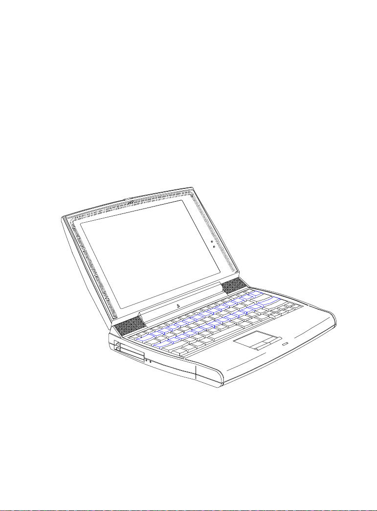
AcerNote 970
Service Guide
Page 2

About this Manual
Purpose
This service guide contains reference information for the 370 notebook computer. It gives the
system and peripheral specifications, shows how to identify and solve system problems and
explains the procedure for removing and replacing system components. It also gives information
for ordering spare parts.
Manual Structure
This service guide consists of four chapters and seven appendices as follows:
Chapter 1 Introduction
This chapter gives the technical specifications for the notebook and its peripherals.
Chapter 2 Major Chip Descriptions
This chapter lists the major chips used in the notebook and includes pin descriptions and
related diagrams of these chips.
Chapter 3 BIOS Setup Information
This chapter includes the system BIOS information, focusing on the BIOS setup utility.
Chapter 4 Disassembly and Unit Replacement
This chapter tells how to disassemble the notebook and replace components.
Appendix A Model Number Definition
This appendix lists the model number definition of this notebook model series.
Appendix B Exploded View Diagram
This appendix shows the exploded view diagram of the notebook.
Appendix C Spare Parts List
This appendix contains spare parts information.
Appendix D Schematics
This appendix contains the schematic diagrams of the notebook.
Page 3

Appendix E BIOS POST Checkpoints
This appendix lists all the BIOS POST checkpoints.
Appendix F Forms
This appendix contains standard forms that can help improve customer service.
Related product information
AcerNote 970 User's Manual contains system description and general operating instructions.
Vesuvius-LS Chipset Data Sheets contain information on the system core chips (V1-LS, V2-LS,
V3-LS).
NMG2090 Data Sheet contains detailed information on the NeoMagic VGA controller.
RCV288Aci/SVD Chipset Data Sheet contains detailed information on the Rockwell Modem
controller.
ESS1688W Data Sheet contains detailed information on the ESS audio controller.
87C552 Data Sheet contains detailed information on the Philips System Management Controller.
NS87336VLJ Data Sheet contains detailed information on the NS super I/O controller.
CL-PD6730 Data Sheet contains detailed information on the Cirrus Logic PCMCIA controller.
PCI0643 Data Sheets contain detailed information on the CMD PCI IDE controller.
T62.036.C , T62.039. and C T62.055.C Data Sheets contain detailed information on the Ambit
components.
M38802 Data Sheet contains detailed information on the Phoenix keyboard controller.
Page 4
Conventions
The following are the conventions used in this manual:
Text entered by user Represents text input by the user.
Screen messages
Denotes actual messages that appear onscreen.
a, e, s, etc. Represent the actual keys that you have to press on the
keyboard.
NOTE
Gives bits and pieces of additional information related to the
current topic.
WARNING
Alerts you to any damage that might result from doing or not
doing specific actions.
CAUTION
Gives precautionary measures to avoid possible hardware or
software problems.
IMPORTANT
Reminds you to do specific actions relevant to the
accomplishment of procedures.
TIP
Tells how to accomplish a procedure with minimum steps
through little shortcuts.
Page 5

Table of Contents
Chapter 1 System Introduction
1.1 Overview..............................................................................................................1-1
1.1.1 Features.................................................................................................1-1
1.1.2 FlashStart - Turning the Notebook Computer On and Off.......................1-2
1.1.3 Ports......................................................................................................1-3
1.1.4 Automatic Tilt-up Keyboard....................................................................1-4
1.1.5 Indicator Light........................................................................................1-5
1.1.6 Keyboard Hotkey List.............................................................................1-6
1.2 System Specification Overview ............................................................................1-9
1.3 Board Layout ...................................................................................................... 1-11
1.3.1 System Board (Top Side).....................................................................1-12
1.3.2 System Board (Bottom Side) ................................................................1-13
1.3.3 Media Board (Top Side).......................................................................1-14
1.3.4 Media Board (Bottom Side)..................................................................1-15
1.3.5 CPU Board(Top Side) .......................................................................... 1-16
1.3.6 CPU Board (Bottom Side)....................................................................1-16
1.4 Jumpers and Connectors....................................................................................1-17
1.5 System Configurations and Specifications ..........................................................1-21
1.5.1 Memory Address Map..........................................................................1-21
1.5.2 Interrupt Channel Map..........................................................................1-21
1.5.3 I/O Address Map..................................................................................1-22
1.5.4 DMA Channel Map ...............................................................................1-23
1.5.5 GPIO Port Definition Map ....................................................................1-23
1.5.6 PCI Devices Assignment...................................................................... 1-27
1.5.7 Power Management.............................................................................1-28
1.5.8 CPU.....................................................................................................1-35
1.5.9 BIOS....................................................................................................1-35
1.5.10 System Memory...................................................................................1-36
1.5.11 Cache Memory.....................................................................................1-37
1.5.12 Video Memory......................................................................................1-37
1.5.13 Video Display Modes............................................................................1-37
1.5.14 Audio ................................................................................................... 1-38
1.5.15 Modem.................................................................................................1-39
Page 6

1.5.16 PCMCIA...............................................................................................1-39
1.5.17 Parallel Port.........................................................................................1-40
1.5.18 Serial Port............................................................................................1-40
1.5.19 Touchpad.............................................................................................1-40
1.5.20 SIR ......................................................................................................1-41
1.5.21 LCD .....................................................................................................1-41
1.5.22 CD-ROM..............................................................................................1-42
1.5.23 Diskette Drive ......................................................................................1-42
1.5.24 Hard Disk Drive....................................................................................1-43
1.5.25 Keyboard .............................................................................................1-43
1.5.26 Battery.................................................................................................1-44
1.5.27 DC-DC Converter.................................................................................1-44
1.5.28 DC-AC Inverter ....................................................................................1-44
1.5.29 AC Adapter ..........................................................................................1-45
1.6 System Block Diagrams......................................................................................1-46
1.6.1 System Functional Block Diagram........................................................1-46
1.6.2 System Bus Block Diagram..................................................................1-47
1.7 Environmental Requirements ..............................................................................1-48
1.8 Mechanical Specifications...................................................................................1-49
Chapter 2 Major Chips Description
2.1 Major Component List.......................................................................................... 2-1
2.2 PicoPower Vesuvius-LS Chipset.......................................................................... 2-2
2.2.1 PT86C521(V1-LS) System Controller.................................................... 2-8
2.2.2 PT86C522(V2-LS) Data Path Controller...............................................2-18
2.2.3 PT86C523(V3-LS) PCI to ISA Controller..............................................2-22
2.3 NM2090 Video Controller....................................................................................2-28
2.3.1 Features...............................................................................................2-29
2.3.2 Pin Diagram.........................................................................................2-31
2.3.3 Pin Description .....................................................................................2-32
2.4 Rockwell RCV288Aci/SVD Modem Chipset.........................................................2-42
2.4.1 R6723-12 MCU (Microcomputer) Chip..................................................2-45
2.4.2 R6684-17 MDP (Modem Data Pump) Chip...........................................2-49
2.4.3 R6693-14 DTP (DigiTalk Processor) Chip ............................................2-53
Page 7

2.5 ESS1688W Sound Controller..............................................................................2-56
2.5.1 Block Diagram .....................................................................................2-56
2.5.2 Pin Diagram.........................................................................................2-57
2.5.3 Pin Descriptions................................................................................... 2-58
2.6 Philips 87C552 System Management Controller .................................................2-63
2.6.1 Features...............................................................................................2-63
2.6.2 Block Diagram .....................................................................................2-64
2.6.3 Pin Diagram.........................................................................................2-65
2.6.4 Pin Descriptions................................................................................... 2-66
2.7 NS87336VLJ Super I/O Controller ......................................................................2-68
2.7.1 Features...............................................................................................2-68
2.7.2 Block Diagram .....................................................................................2-70
2.7.3 Pin Diagram.........................................................................................2-71
2.7.4 Pin Description..................................................................................... 2-72
2.8 CL-PD6730 PCI PCMCIA Controller ................................................................... 2-80
2.8.1 Features...............................................................................................2-80
2.8.2 Pin Diagram.........................................................................................2-81
2.8.3 Pin Descriptions................................................................................... 2-81
2.9 PCI0643 PCI E-IDE Controller............................................................................2-91
2.9.1 Features...............................................................................................2-91
2.9.2 Pin Diagram.........................................................................................2-92
2.9.3 Signal Descriptions ..............................................................................2-93
2.10 Ambit T62.036.C DC-DC Converter................................................................... 2-97
2.10.1 Pin Diagram.........................................................................................2-97
2.10.2 Pin Descriptions................................................................................... 2-97
2.11 Ambit T62.039.C/T62.055.C DC-AC Inverter ......................................................2-99
2.11.1 Pin Diagram.........................................................................................2-99
2.11.2 Pin Descriptions................................................................................... 2-99
Chapter 3 BIOS Setup Information
3.1 When to Use Setup...............................................................................................3-1
3.2 Entering Setup......................................................................................................3-2
3.3 About My Computer..............................................................................................3-3
3.4 System Configuration ...........................................................................................3-5
Page 8

3.4.1 Date and Time ...................................................................................... 3-5
3.4.2 Diskette Drives...................................................................................... 3-5
3.4.3 Hard Disks ............................................................................................ 3-6
3.4.4 Num Lock After Boot............................................................................. 3-6
3.4.5 LCD Expansion Mode ........................................................................... 3-6
3.4.6 Internal Cache....................................................................................... 3-8
3.4.7 External Cache ..................................................................................... 3-8
3.4.8 Enhanced IDE Features........................................................................ 3-8
3.4.9 Onboard Communication Ports ............................................................. 3-9
3.4.10 Onboard Audio.....................................................................................3-11
3.4.11 Reset PnP Resources ..........................................................................3-12
3.5 Power Saving Options ........................................................................................3-13
3.5.1 When Lid is Closed..............................................................................3-13
3.5.2 Suspend to Disk on Critical Battery ......................................................3-14
3.5.3 Display Always On ...............................................................................3-14
3.5.4 Internal Speaker...................................................................................3-14
3.5.5 External Mouse Location......................................................................3-14
3.5.6 Internal Modem....................................................................................3-15
3.5.7 Resume On Modem Ring.....................................................................3-15
3.5.8 Resume On Schedule..........................................................................3-15
3.5.9 Resume Date / Resume Time..............................................................3-15
3.6 System Security..................................................................................................3-16
3.6.1 Supervisor and User Passwords...........................................................3-16
3.6.2 Diskette Drive Control..........................................................................3-17
3.6.3 Hard Disk Drive Control .......................................................................3-18
3.6.4 Start Up Sequences.............................................................................3-18
3.6.5 Flash New BIOS...................................................................................3-18
3.7 Reset to Default Settings ....................................................................................3-20
Chapter 4 Disassembly and Unit Replacement
4.1 General Information............................................................................................. 4-2
4.1.1 Before You Begin.................................................................................. 4-2
4.1.2 Connector Types................................................................................... 4-3
4.1.3 Disassembly Sequence......................................................................... 4-4
4.2 Removing the Module.......................................................................................... 4-6
Page 9

4.3 Removing the Keyboard .......................................................................................4-7
4.3 Removing or Replacing the CPU ..........................................................................4-9
4.4 Removing the Display .........................................................................................4-10
4.5 Disassembling the Housing.................................................................................4-11
4.5.1 Detaching the Lower Housing from the Inside Assembly ......................4-11
4.5.2 Replacing the Hard Disk Drive ............................................................. 4-12
4.5.3 Replacing Memory............................................................................... 4-12
4.5.4 Detaching the Upper Housing from the Inside Assembly ...................... 4-14
4.5.5 Removing the Touchpad...................................................................... 4-15
4.5.6 Removing the Main Board....................................................................4-16
4.5 Disassembling the Display..................................................................................4-18
Appendix A Model Number Definition
Appendix B Exploded View Diagram
Appendix C Spare Parts List
Appendix D Schematics
Appendix E BIOS POST Checkpoints
Appendix F Technical Bulletins and Updates
Appendix G Forms
Page 10

List of Figures
1- 1 FlashStart Automatic Power-on Switch (Lid Switch)............................................. 1-2
1- 2 Ports.................................................................................................................... 1-3
1- 3 Indicator Lights .................................................................................................... 1-5
1- 4 System Board (Top Side) ....................................................................................1-12
1- 5 System Board (Bottom Side)...............................................................................1-13
1- 6 Media Board (Top Side)......................................................................................1-14
1- 7 Media Board (Bottom Side) .................................................................................1-15
1- 8 CPU board(Top Side)..........................................................................................1-16
1- 9 CPU board (Bottom Side) ...................................................................................1-16
1- 10 Mainboard Jumpers and Connectors (Top Side)..................................................1-17
1- 11 Mainboard Jumpers and Connectors (Bottom Side) ............................................1-18
1- 12 Media Board Jumpers and Connectors (Top Side)..............................................1-19
1- 13 Media Board Jumpers and Connectors (Bottom Side).........................................1-20
1- 14 System Functional Block Diagram ......................................................................1-46
1- 15 System Bus Block Diagram.................................................................................1-47
2-1 Architecture Block Diagram.................................................................................. 2-7
2-2 PT86C521(V1-LS) Block Diagram........................................................................ 2-8
2-3 PT86C521(V1-LS) Pin Diagram........................................................................... 2-9
2-4 PT86C522(V2-LS) Block Diagram.......................................................................2-18
2-5 PT86C522(V2-LS) Pin Diagram..........................................................................2-19
2-6 PT86C521(V3-LS) Block Diagram.......................................................................2-22
2-7 PT86C521(V3-LS) Pin Diagram..........................................................................2-23
2-8 NMG2090 Pin Diagram.......................................................................................2-31
2-9 RCV288Aci/SVD Architecture Block Diagram.....................................................2-44
2-10 R6723-12 Pin Diagram........................................................................................2-45
2-11 R6684-17 Pin Diagram........................................................................................2-49
2-12 R6693-14 Pin Diagram........................................................................................2-53
2-13 ESS1688W Block Diagram.................................................................................2-56
2-14 ESS1688W Pin Diagram.....................................................................................2-57
2-15 87C552 Block Diagram.......................................................................................2-64
2-16 87C552 Pin Diagram...........................................................................................2-65
2-13 NS87336VLJ Block Diagram...............................................................................2-70
2-14 NS87336VLJ Pin Diagram..................................................................................2-71
2-19 PCI0643 Pin Diagram.........................................................................................2-92
Page 11

2-20 T62.036.C Pin Diagram......................................................................................2-97
2-21 T62.039.C/T62.055.C Pin Diagram.....................................................................2-99
4-1 Removing the Battery Pack..................................................................................4-2
4-2 Using Plastic Stick on Connector With Lock..........................................................4-3
4-3 Disassembly Flow .................................................................................................4-5
4-4 Removing the Module...........................................................................................4-6
4-5 Removing the Display Hinge Covers.....................................................................4-7
4-6 Removing the Center Hinge Cover.......................................................................4-7
4-7 Lifting Out the Keyboard.......................................................................................4-8
4-8 Unplugging the Keyboard Connectors and Removing the Keyboard......................4-8
4-9 Removing the CPU Module Lock..........................................................................4-9
4-10 Removing the CPU Module ..................................................................................4-9
4-11 Unplugging the Display Cable.............................................................................4-10
4-12 Removing the Display Hinge Screws and Removing the Display.........................4-10
4-13 Removing the Hard Disk Drive Bay Cover.......................................................... 4-11
4-14 Removing the Hard Disk Drive Bay Cover.......................................................... 4-12
4-15 Installing and Removing Memory........................................................................4-13
4-16 Installing a Memory Module via the Memory Door .............................................. 4-13
4-17 Removing the Battery Bay Screws...................................................................... 4-14
4-18 Detaching the Upper Housing from the Inside Frame Assembly.......................... 4-14
4-19 Removing the Touchpad.....................................................................................4-15
4-20 Unplugging the Speaker Connectors and Battery Pack Connector......................4-16
4-21 Removing the Main Board..................................................................................4-16
4-22 Removing the Charger Board and Multimedia Board..........................................4-17
4-23 Removing the PC Card Slots..............................................................................4-17
4-24 Removing the LCD Bumpers..............................................................................4-18
4-25 Removing the Display Bezel Screws...................................................................4-18
4-26 Removing the Display Bezel...............................................................................4-19
4-27 Removing the Display Panel Screws and the Display Connectors .......................4-19
4-28 Removing the Display Cable Assembly............................................................... 4-20
Page 12

List of Tables
1-1 Port Descriptions.................................................................................................. 1-4
1-2 Indicator Status Descriptions................................................................................ 1-5
1-3 Hotkey List Descriptions....................................................................................... 1-6
1-4 Eject Menu Descriptions ...................................................................................... 1-8
1-5 System Specifications.......................................................................................... 1-9
1-6 Mainboard Jumpers Pads Settings (Bottom Side)...............................................1-18
1-7 Memory Address Map.........................................................................................1-21
1-8 Interrupt Channel Map........................................................................................1-21
1-9 I/O Address Map .................................................................................................1-22
1-10 DMA Channel Map..............................................................................................1-23
1-11 GPIO Port Definition Map...................................................................................1-23
1-12 PCI Devices Assignment.....................................................................................1-27
1-13 PMU Timers List.................................................................................................1-28
1-14 CPU Specifications.............................................................................................1-35
1-15 BIOS Specifications ............................................................................................1-35
1-16 System Memory Specifications...........................................................................1-36
1-17 SIMM memory combination list...........................................................................1-36
1-18 Cache Memory Specifications.............................................................................1-37
1-19 Video Memory Specification ...............................................................................1-37
1-20 Video Display Specification.................................................................................1-37
1-21 External CRT Resolution Modes.........................................................................1-38
1-22 LCD Resolution Modes.......................................................................................1-38
1-23 Audio Specifications ...........................................................................................1-38
1-24 Modem Specifications.........................................................................................1-39
1-25 PCMCIA Specifications.......................................................................................1-39
1-26 Parallel Port Specifications.................................................................................1-40
1-27 Serial Port Specifications ....................................................................................1-40
1-28 Touchpad Specifications .....................................................................................1-40
1-29 SIR Specifications...............................................................................................1-41
1-30 LCD Specifications .............................................................................................1-41
1-31 CD-ROM Specifications......................................................................................1-42
1-32 Diskette Drive Specifications ..............................................................................1-42
1-33 Hard Disk Drive Specifications............................................................................1-43
1-34 Keyboard Specifications......................................................................................1-43
Page 13

1-35 Battery Specifications......................................................................................... 1-44
1-36 DC-DC Converter Specifications.........................................................................1-44
1-37 DC-AC Inverter Specifications............................................................................1-45
1-38 AC Adapter Specifications..................................................................................1-45
1-39 Environmental Requirements..............................................................................1-48
1-40 Mechanical Specifications...................................................................................1-49
2-1 Major Chips List ....................................................................................................2-1
2-2 V1-LS Pin Descriptions.......................................................................................2-10
2-3 V2-LS Pin Descriptions.......................................................................................2-20
2-4 V3-LS Pin Descriptions.......................................................................................2-24
2-5 NMG2090 Pin Description Conventions.............................................................. 2-32
2-6 NMG2090 Pin Descriptions .................................................................................2-32
2-7 RCV288Aci/SVD Signal Type Annotation............................................................2-44
2-8 R6723-12 Pin Descriptions..................................................................................2-46
2-9 R6684-17 Pin Descriptions (MDP).......................................................................2-50
2-10 R6693-14 Pin Descriptions..................................................................................2-54
2-11 ESS1688W Pin Descriptions...............................................................................2-58
2-12 87C552 Pin Descriptions.....................................................................................2-66
2-10 NS87336VLJ Pin Descriptions............................................................................2-72
2-14 CL-PD6730 Pin Descriptions...............................................................................2-83
2-15 PCI0643 Signal Descriptions...............................................................................2-93
2-16 T62.036.C Pin Descriptions.................................................................................2-97
2-17 T62.039.C/T62.055.C Pin Descriptions...............................................................2-99
3-1 About My Computer Item Descriptions..................................................................3-4
3-2 Diskette Drive Control Settings........................................................................... 3-17
3-3 Hard Disk Drive Control Settings.........................................................................3-18
3-4 Start Up Sequences Settings..............................................................................3-18
3-5 Error Beep Sequences During the Boot ROM Process........................................3-19
4-1 Guide to Disassembly Sequence ..........................................................................4-4
Page 14

C h a p t e r 1C h a p t e r 1
Introduction
This chapter introduces the notebook computer, and describes its features and specifications.
1.1. Overview
This Pentium-based notebook computer combines high-performance, versatility, multimedia
capabilities and a truly advanced power management system.
1.1.1 Features
PERFORMANCE
• Mobile Pentium microprocessor (P54CSLM-120/133/150)
• 64-bit DIMM memory architecture
• 256KB or 512 KB external (L2) cache memory
• Large display in DualScan STN(11.3”) or active-matrix TFT(11.8” or 12.1”)
• PCI local bus video with 128-bit graphics accelerator
• Flexible module bay (3.5-inch floppy drive or CD-ROM drive)
• High-capacity, Enhanced-IDE hard disk
• Heuristic power management with suspend-to-memory and zero-volt suspend-to-disk power-
saving modes
• Lithium-Ion smart battery pack
• High speed connectivity
• 16-bit stereo audio with built-in FM synthesizer
• Built-in microphone and dual angled stereo speakers
• 30fps (frames per second) full-screen, true-color MPEG video playback
• Infrared wireless communication
• Internal 28.8Kbps modem with DSVD (digital simultaneous voice over data) support; with
speakerphone and telephone answering device features
HUMAN-CENTRIC DESIGN AND ERGONOMICS
• Intuitive FlashStart automatic power-on
Page 15

• Sleek, smooth and stylish design
• Automatic tilt-up, full-sized, full-function keyboard
• Wide and comfortable palm rest
• Ergonomically-centered touchpad pointing device
EXPANSION
• PC Card (formerly PCMCIA) slots (two type II/I or one type III)
• Mini dock option with built-in Ethernet
• User-upgradeable memory
1.1.2 FlashStart - Turning the Notebook Computer On and Off
A noticeably unique feature about this notebook is that it has no on/off switch. Instead it employs
a lid switch, located near the center of the display hinge, that tells the notebook when it should
wake up or go to sleep.
Figure 1- 1 FlashStart Automatic Power-on Switch (Lid Switch)
When you close the display lid, the notebook enters suspend-to-memory or suspend-to-disk mode
before turning off the power, depending on the When Lid is Closed parameter setting in BIOS
Setup. When you open the lid, the notebook resumes from where you left off before closing the
lid.
Suspend-to-memory, suspend-to-disk and other power management issues are discussed in detail
in power management section.
Page 16
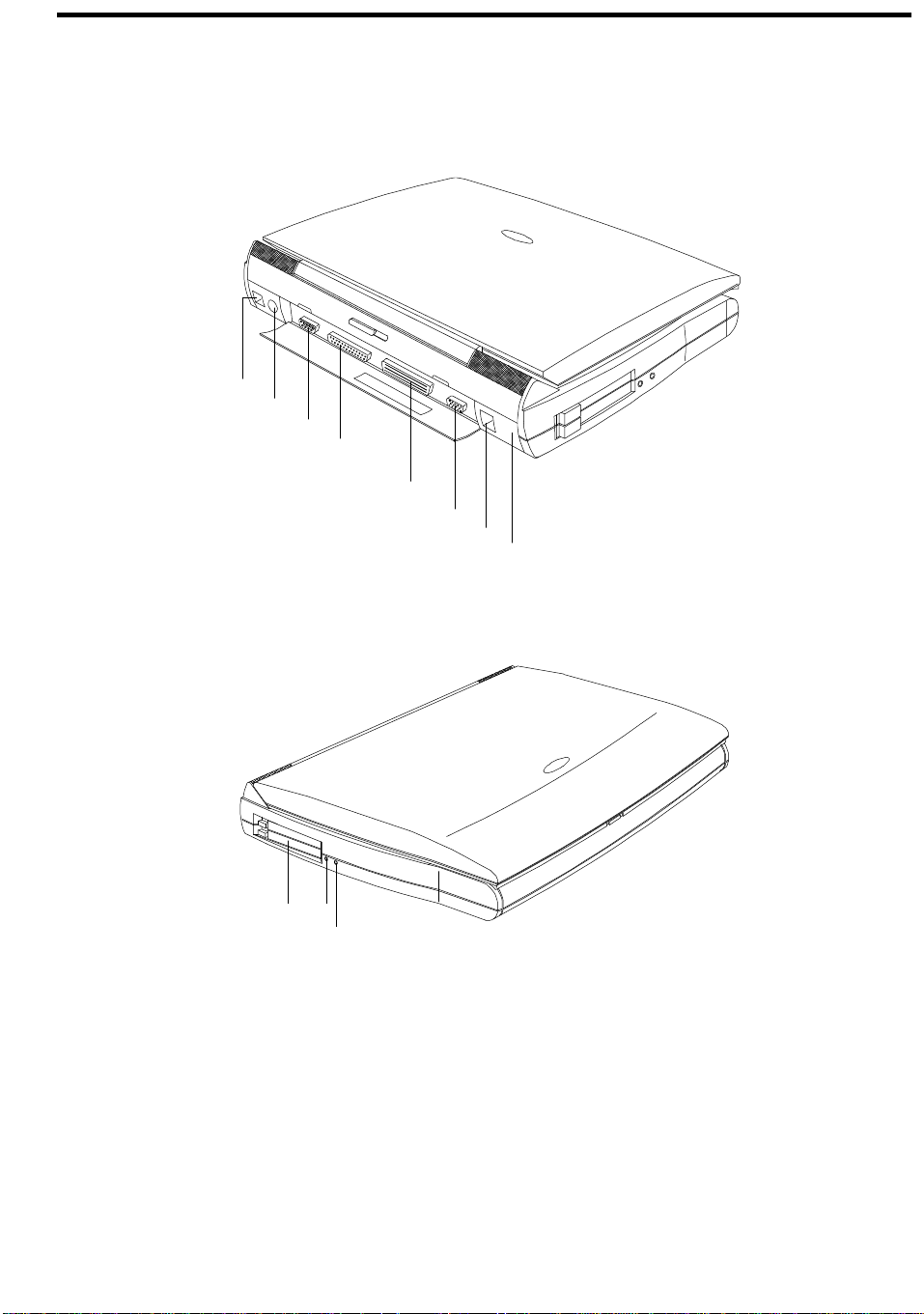
1.1.3 Ports
The notebook computer’s ports are found on the rear and left panel.
1
2
3
4
5
6
7
8
10
9
11
1 DC-in Port 7 RJ-11 Phone Jack
2 PS/2 Port 8 Infrared Port
3 Serial Port 9 PC Card Slots
4 Parallel Port 10 Microphone-in/Line-in Jack
5 Mini Dock Connector 11 Speaker-out/Line-out Jack
6 External CRT Port
Figure 1- 2 Ports
Page 17
The following table describes the ports.
Table 1- 1 Port Descriptions
# Icon Port Connects to...
Rear Panel Ports
1 DC-in port AC adapter and power outlet
2
3 Serial port
4 Parallel port
5 Mini dock connector Mini dock
6 External CRT port External monitor (up to 1024x768, 256 colors )
7 Modem jack (RJ-11) Phone line
8 Infrared port Infrared-aware device (e.g., notebook with IR
Left Panel Ports
9 PC Card slots One Type III or two Type I/II PC cards
10 Microphone-in/Line-in External microphone or line input device
PS/2 port PS/2-compatible device (e.g., PS/2 keyboard,
keypad, mouse)
Serial device (e.g., serial mouse)
(UART16650-compatible)
Parallel device (e.g., parallel printer, floppy drive
(EPP/ECP-compliant)
module when used externally)
port, desktop with IR adapter, IR-capable
printer)
11 Speaker-out/Line-out Amplified speakers or headphones
1.1.4 Automatic Tilt-up Keyboard
A tilt switch, found right above the port cover on the rear of the notebook, allows you to enable or
disable this feature. Follow these steps:
1. Close the lid. 2. To enable, slide the tilt
switch to the right ( ).
To disable, slide the tilt
switch to the left ( ).
3. Open the lid.
Page 18
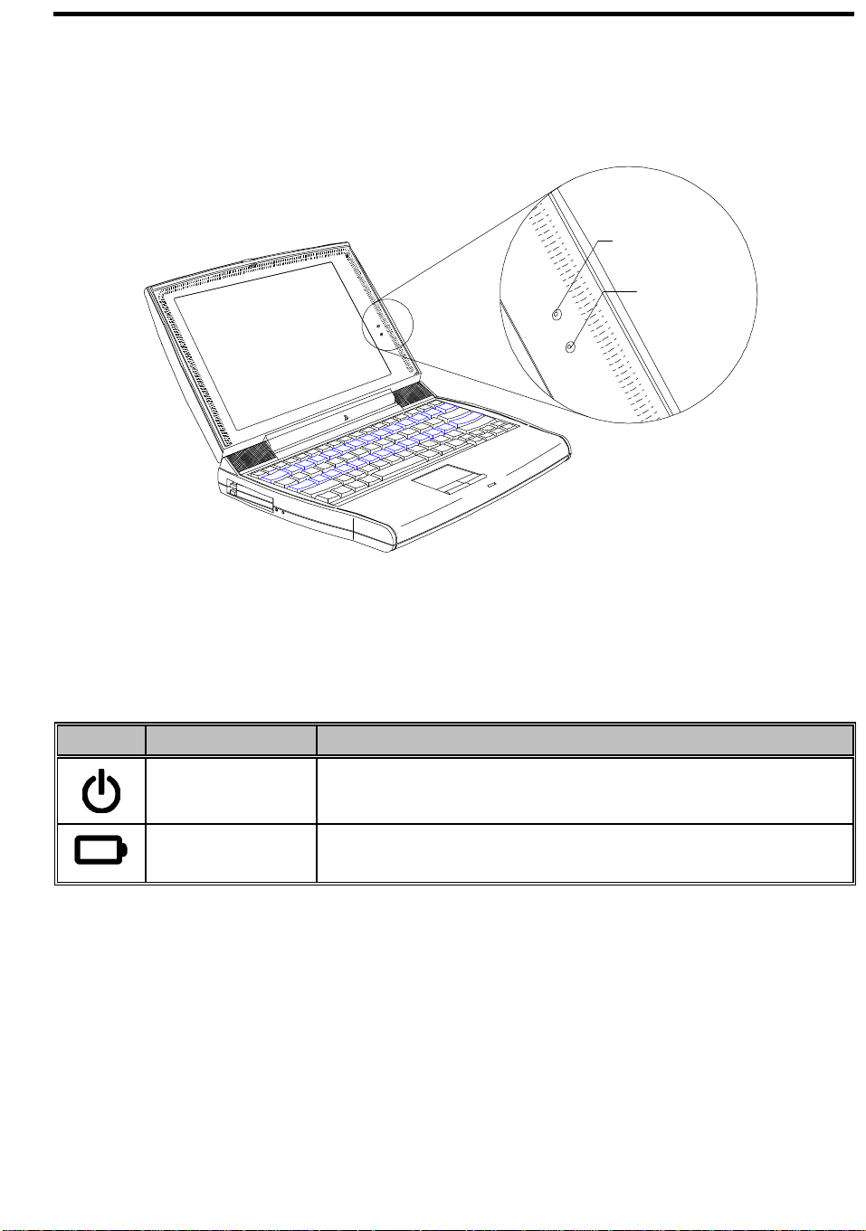
1.1.5 Indicator Light
Indicator
Two indicator lights are found on the display panel.
Power
Battery
Indicator
Figure 1- 3 Indicator Lights
These indicators and their descriptions are shown in the table below.
Table 1- 2 Indicator Status Descriptions
Icon Indicator Light Description
Power Indicator • Lights when power is on
• Flashes when the notebook is in suspend-to-memory mode
Battery Indicator • Lights when battery pack is charging
• Flashes when battery power is low
Page 19
1.1.6 Keyboard Hotkey List
The following table lists and describes the hotkeys used by the notebook computer.
Table 1- 3 Hotkey List Descriptions
Hotkey Icon Function Description
Fn-Esc Suspend-to-memory Enters suspend-to-memory mode
Fn-F1
Help Displays the hotkey menu
?
Fn-F2 Setup Enters the BIOS Setup utility
Fn-F3
Fn-F4 Screen Blackout Blanks the screen to save power. To wake up the screen,
Fn-F5 Display Toggle Switches display from LCD to CRT to both LCD and CRT
Fn-F6 Fuel Gauge On/Off Toggles battery gauge display on/off.
Fn-F7 Speaker On/Off Toggles speaker output on and off
Fn-F8 Lock System
PnP
Plug and Play
Configuration
Resources
Allows the system to re-configure itself and do selfdiagnostics
press any key.
Also shows the following:
• “plug” icon if a powered AC adapter is connected to the
notebook.
• “speaker” icon if speaker output is on (toggled by Fn-F7).
• “T” icon if turbo mode is on (toggled by Fn-2).
Provides notebook security by locking system from access.
Requires password input to unlock system.
Page 20
Table 1- 3 Hotkey List Descriptions
Hotkey Icon Function Description
Fn-F9 Eject Accesses the Eject menu. See the following subsection.
Fn-Ctrl-↑ Volume Up Increases audio volume
Fn-Ctrl-↓ Volume Down Decreases audio volume
Fn-Ctrl-← Balance Left Shifts speaker balance to the left
Fn-Ctrl-→ Balance Right Shifts speaker balance to the right
Fn-ÿ-↑ Brightness Up Increases screen brightness
Fn-ÿ-↓ Brightness Down Decreases screen brightness to save power
Fn-ÿ-→ Contrast Up Increases screen contrast (DSTN only)
Fn-ÿ-← Contrast Down Decreases screen contrast (DSTN only)
Fn-↑ Fuel Gauge Up With the fuel gauge onscreen, moves the fuel gauge up
Fn-↓ Fuel Gauge Down With the fuel gauge onscreen, moves the fuel gauge down
Fn-← Fuel Gauge Left With the fuel gauge onscreen, moves the fuel gauge left
Fn-→ Fuel Gauge Right With the fuel gauge onscreen, moves the fuel gauge right
Fn-1 CD Eject Ejects the CD-ROM drive
Fn-2 Turbo Mode On/Off Toggles turbo mode on and off.
Page 21

1.1.6.1 Using the Eject Menu
Pressing Fn-F9 brings up the Eject Menu.
Eject Menu
Battery (Suspend to Disk).............. Change
CD-ROM Disc (Also Fn+1)................
Power Off (Also Fn+BackSpace x3).......
↑↑↓↓ = Move Highlight Bar, ↵↵ = Select, Esc = Exit
The eject menu commands allow you to perform various eject-related functions for the notebook.
See the following table for details
Table 1- 4 Eject Menu Descriptions
Select… To…
Battery Change the battery.
This option forces the notebook to enter suspend-to-disk mode, so that you can replace
the battery with a charged one, and then return to where you left off.
To resume, close the display lid and open the display lid again.
CD-ROM Disc Open the CD-ROM drive.
There are many ways to open the CD-ROM disc tray:
• selecting this option
• pressing Fn-1
• pressing the CD-ROM eject button
• using software controls
It is best to wait for the CD-ROM light (found on the CD-ROM eject button) to go off
before ejecting the CD-ROM drive.
Power Off Turn the system off (without entering suspend-to-disk mode).
When you choose this option, a “cold boot” occurs after re-starting the system (opening
and closing the display). You can choose this option when you want to swap modules,
or when you want to turn off the notebook without entering any of the suspend modes.
To turn the notebook back on, close the display lid and open the display lid again.
Page 22

1.2. System Specification Overview
Table 1- 5 System Specifications
Item Standard Optional
Microprocessor Mobile Intel Pentium™ processor
(133/150MHz)
Memory
System / Main
16MB
Dual 64-bit memory banks
Expandable to 64MB using 8/16/32MB
soDIMMs
External cache
System BIOS 256KB (Boot Block Flash ROM)
Storage system One 2.5-inch, high-capacity Enhanced-IDE
Display DualScan STN or active-matrix TFT LCD,
Video system PCI local bus video with 128-bit graphics
Audio system 16-bit stereo audio with built-in FM
Communications
system
Operating
system
Keyboard and
pointing device
256KB L2 cache (synchronous SRAM)
hard disk
One high-speed IDE CD-ROM drive module
One 3.5-inch, 1.44MB floppy drive module
(internal/external use)
800x600, 64K colors (SVGA)
accelerator
synthesizer
Built-in microphone and dual angled
speakers
Built-in V.34 fax/data modem (28.8Kbps)
with digital simultaneous voice over data
(DSVD) support
Windows 95 DOS and Windows 3.x, OS/2 Warp
84-/85-key with Win95 keys;
auto-tilt feature
512KB L2 cache
Higher-capacity E-IDE hard disk
Up to 1024x768, 256-color ultra-VGA
monitor
LCD projection panel
PC card modem
101-/102-key, PS/2-compatible
keyboard or 17-key numeric keypad
Touchpad (centrally-located on palm rest)
I/O ports One 9-pin RS-232 serial port
(UART16550-compatible)
One 25-pin parallel port
(EPP/ECP-compliant)
One 15-pin CRT port
External serial or PS/2 mouse or
similar pointing device
Serial mouse, printer or other serial
devices
Parallel printer or other parallel
devices; floppy drive module (when
used externally)
Up to a 1024x768 ultra-VGA monitor
Page 23

Table 1- 5 System Specifications
Item Standard Optional
One 6-pin PS/2 connector
17-key numeric keypad, PS/2
keyboard, mouse or trackball
One 240-pin mini dock connector
One type III or two type II PC Card slot(s)
One serial infrared port (IrDA-compliant)
One 3.5mm minijack microphone-in/line-in
jack
One 3.5mm minijack speaker-out/line-out
jack
RJ11 phone jack
Weight
with FDD
with CD-ROM
Dimensions
Round contour
Main footprint
Temperature
Operating
Non-operating
Humidity
Operating
Non-operating
AC adapter 100~240Vac, 50~60Hz autosensing AC
Battery pack
Type
(includes battery)
3.4 kg. (7.4 lbs.)
3.5 kg. (7.7 lbs.)
L x W x H
297~313mm x 230~240mm x 48~53mm
11.7” x 9.1” x 2”
10ºC ~ 35ºC
-10ºC ~ 60ºC
(non-condensing)
20% ~ 80% RH
20% ~ 80% RH
adapter
58.3WH Lithium-Ion battery with intelligent
charging and built-in battery gauge
Mini dock
LAN card or other PC cards
External IR devices and peripherals
Microphone or line-in device
Speakers or headphones
Carrying bag
Extra AC adapter
Extra battery pack
Charge time
2.0-hour rapid-charge
3.0-hour charge-in-use
Page 24
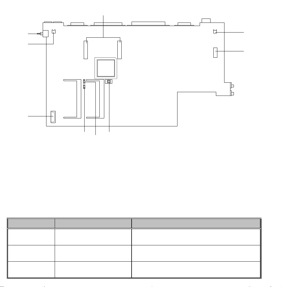
1.4. Jumpers and Connectors
CN4 CN6 CN9
U1
CN11
CN2
CN3
CN5 CN8, CN12
CN4 Modem RJ11 phone jack
CN6 VGA port
CN9 Mini dock port
CN13 Parallel port
CN14 Serial Port
CN15 PS2 mouse/keyboard port
CN16 AC adapter plug-in port
CN13
CN10, CN7 Multimedia board connector
CN11 FDD/CD-ROM connector
CN12, CN8 CPU board connector
CN5 Hard disk drive connector
CN3 Speaker-out/Line-out Jack
CN2 Microphone-in/Line-in Jack
U1 SIR infrared LED
CN14
CN15
CN16
CN10
CN7
Figure 1- 10 Mainboard Jumpers and Connectors (Top Side)
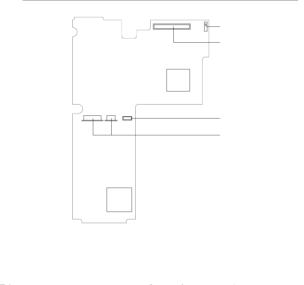
Page 25
CN20, CN19
SW1
CN23
CN21
PAD21 PAD19
PAD20
CN20, CN19 DC-DC converter connector
CN17 Left speaker connector
CN18 Debug port
PAD19 Keyboard type setting pad
PAD21 Password setting pad
CN21 Battery connector
CN23 Right speaker connector
SW1 Reset Switch
PAD20 BIOS type setting pad
Figure 1- 11 Mainboard Jumpers and Connectors (Bottom Side)
CN17
CN18
Table 1- 6 Mainboard Jumpers Pads Settings (Bottom Side)
Jumper Pad Descriptions Settings
PAD19 Keyboard type selection Open: Other keyboard
Short: Japan keyboard
PAD20 BIOS type selection Open: Acer BIOS
Short: OEM BIOS
PAD21 Password settings Open: Enable password
Short: Bypass password
Page 26
CN7
CN6
CN5
CN2, CN4
CN7 Lid switch
CN6 LCD connector
CN5 Touchpad connector
CN4, CN2 Keyboard connector
Figure 1- 12 Media Board Jumpers and Connectors (Top Side)
Page 27
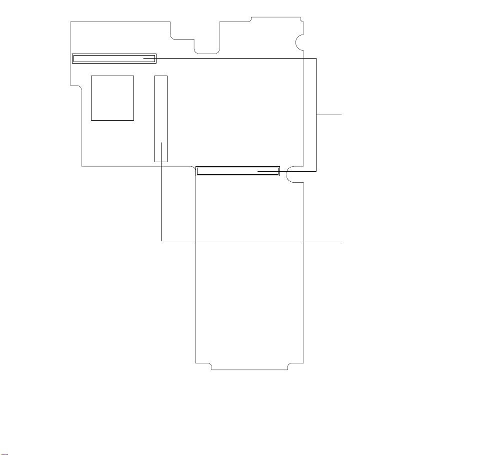
CN10, CN8
CN9
CN10, CN8 Mainboard connector CN9 PCMCIA socket connector
Figure 1- 13 Media Board Jumpers and Connectors (Bottom Side)
Page 28
1.5. System Configurations and Specifications
1.5.1 Memory Address Map
Table 1- 7 Memory Address Map
Address Range Definition Function
000000 - 09FFFF 640 KB memory Base memory
0A0000 - 0BFFFF 128 KB video RAM Reserved for graphics display buffer
0C0000 - 0CBFFF Video BIOS Video BIOS
0F0000 - 0FFFFF 64 KB system BIOS System BIOS
100000 - top limited Extended memory SIMM memory
FE0000 - FFFFFF 256 KB system ROM Duplicate of code assignment at 0E0000-0FFFFF
1.5.2 Interrupt Channel Map
Table 1- 8 Interrupt Channel Map
Interrupt Number Interrupt Source (Device Name)
IRQ 0
IRQ 1
IRQ 2
IRQ 3
IRQ 4
IRQ 5
IRQ 6
IRQ 7
IRQ 8
IRQ 9
IRQ 10
IRQ 11
IRQ 12
IRQ 13
IRQ 14
IRQ 15
System Timer
Keyboard
Cascade
IrDA / 2F8h
Serial Port 1 / 3F8h
Audio ESS1688
Floppy Disk Controller (FDC)
Parallel Port
Real Time Clock (RTC)
Ethernet on Port Replicator
Internal Modem / 3E8h
PCMCIA
PS/2 Mouse
Co-processor
Hard disk
CD-ROM
Page 29

1.5.3 I/O Address Map
Table 1- 9 I/O Address Map
Address Range Device
000 - 00F
020 - 021
024, 026, B0h
02E - 02F
040 - 043
048 - 04B
060 - 06E
070 - 071
080 - 08F
0A0 - 0A1
0C0 - 0DF
1F0 - 1F7
3F6 - 3F7
170 - 177
376 - 377
220 - 22F
240 - 24F
260 - 26F
280 - 28F
278 - 27F
2E8 - 2EF
2F8 - 2FF
300 - 301
310 - 311
320 - 321
330 - 321
34C - 34F
378 - 37F
388 - 38B
3BC - 3BE
3B4, 3B5, 3BA
3C0 - 3C5
3C6 - 3C9
3C0 - 3CF
3D0 - 3DF
3E8 - 3EF
3F0 - 3F7
3F8 - 3FF
CF8 - CFF
DMA controller-1
Interrupt controller-1
PicoPower chipset registers
CMD0643 IDE controller
Timer 1
Timer 2
Keyboard controller 8742 chip select
Real-time clock and NMI mask
DMA page register
Interrupt controller-2
DMA controller-2
Hard disk select
Hard disk select
CD-ROM select
CD-ROM select
Audio
Audio - default
Audio
Audio
Parallel port 3
COM 4
COM 2 - IrDA
MPU-401 port - default
MPU-401 port
MPU-401 port
MPU-401 port
Docking station
Parallel port 2
FM synthesizer
Parallel port 1
Video subsystem
Video DAC
Enhanced graphics display
Color graphics adapter
COM3 - Modem
Floppy disk controller
COM 1 - Serial 1
PCI configuration register
Page 30
1.5.4 DMA Channel Map
Table 1- 10 DMA Channel Map
Controller Channel Address Function
1
1
1
1
2
2
2
2
0
1
2
3
4
5
6
7
1.5.5 GPIO Port Definition Map
Table 1- 11 GPIO Port Definition Map
GPIO I/O Description
V1-LS GPIO Pin Assignment
PC0
(VS5_CLKEN)
PC1
(VS5_SUSPEND#)
PC2
(VS5_SPKOFF)
PC3
(VS5_VDCLKEN)
PC4
(VS5_VDPD)
PC5
(VGADIS)
GP0/LED0
(VS5_FLASHRCY)
GP1/LD1/SUSPA#
(VS5_ZZ)
GP2/DDMA_RETRY
(VS5_DDMARETRY)
GP3/SUPPRESS_RESUME
(VS5_COM4_COM3#)
GP4/UNDOCKING
(VS5_FLSHVPP)
GP5/THRM
(SM5_OVTMP)
REQ2#
(PC3_DKREQ#)
O 1: Enable the clock source
O Suspend control (reserved)
O 1: Turn off the speaker
O 1: Video clock enable
O 1: Power down the video controller (in suspend mode)
I 0: Disable VGA controller from PCI
I 1: Flash ROM recover
O Cache sleep
O DDMA (distributed DMA retry). V3-LS activates this pin to retry
V1-LS
O Modem I/O address. 1=2E8h, 0=3E8h.
O 1: Flash ROM Vpp Control
I 1: over temperature alarm from SMC.
I 0: Dock/undock request, used to tri-state PCI bus before
dock/undock.
0087
0083
0081
0082
Cascade
008B
0089
008A
Audio (default)
Audio (option) / ECP
Diskette
Audio (option)
Cascade
Spare
Page 31

Table 1- 11 GPIO Port Definition Map
GPIO I/O Description
GNT2#
(PC5_DKGNT#)
WAKE0
(KB5_KBCSMIREQ#)
WAKE1
(RT5_IRQ8#)
SWITCH
(VS5_DOCKIRQ)
RING
(VS5_Rl#)
EXTACT0
(GR3_VGACT)
87C51 (KBC) GPIO Pin Assignment
LED0 (KB5_KBCSMIREQ#) O KBC SMI request
LED1 (KB5_NUMLED#) O Keyboard number lock LED control
LED2 (KB5_CAPLED#) O Keyboard caps lock LED control
LED3 (KB5_KEYCLICK) O Key-click output
P1.0 (KB5_FPAGE1) O Force BIOS to high page.
P1.1 (KB5_FPAGE2) O FPAGE2 FPAGE1
P1.2 (KB5_IDECLKEN) O Local bus IDE PCI clock enable
P1.3 (KB5_IITCLKEN) O IIT PCI clock enable for video conference
P1.4 (KB5_3MODE) O 0: 3-mode FDD drive
P1.5 {KB5_CDBEN#) O 0: Enable CD-ROM buffer
P1.6 (KB5_HDDBEN# ) O 0: Enable HDD buffer
P1.7 (IS5_IRQ12) O PS2 mouse IRQ12
P2.0 (KB5_MEMIDA0)
P2.1 (KB5_MEMIDA1)
P2.2 (KB5_MODE) I 1: US version (without system power switch)
P2.3 (KB5_FDD/CD#) I 1: FDD installed
O 0: Dock grant, signal for ready to dock/undock.
I 0: Keyboard SMI from KBC and SMC..
I 0: Wake by RTC alarm
I 1: IRQ monitor from docking
I 0: Ring indicator input
I 1: VGA activity from VGA controller ACTIVITY pin.
0 0 F, E0
0 1 F, E1
1 0 F, E2
1 1 reserved
1: Enable FDD buffer
I Memory ID0 and Memory ID1 for SIMM 1.
ID0 ID1 Memory speed
0 0 50nS
0 1 40nS
1 0 70nS
1 1 60nS
0: Japan version ( with ON/RESUME switch)
Page 32

Table 1- 11 GPIO Port Definition Map
GPIO I/O Description
0: CD-ROM installed
P2.4 (KB5_MDMIDB0)
P2.6 (KB5_MDMIDB1)
P2.5 (KB5_PSWD) I 1: Enable password
P2.7 (KB5_OEM) I 1: Enable Acer logo shown on screen while BIOS POST.
P3.0 (SM5_TXD) I UART serial input from SMC.
P3.1 (SM5_RXD) O UART serial output to SMC.
P3.2 (KB5_KBDCLK) I/O External keyboard clock
87C51 (KBC) GPIO Pin Assignment
P3.3 (KB5_PTRCLK) I/O External PS/2 clock
P3.4 (KB5_KBDDAT) I/O External keyboard data
P3.5 (KB5_PTRDAT) I/O External PS/2 data
P3.6 (KB5_TOUCHWR#) O Touchpad write
P3.7 (KB5_TOUCHRD#) O Touchpad read
PCOBF (IS5_IRQ1) O IRQ1
AIN0 (KB5_PANID0)
AIN1 (KB5_PANID1)
AIN2 (KB5_PANID2)
AIN3 (KB5_PANID3)
PCDB0~PCDB7 (ISS_SDx) I ISA data bus
A0 (IS5_SA2) I IO address select: 60h, 64h(for keyboard input buffer)
A1 (IS5_SA1) I IO address select: 60h, 64h(for keyboard input buffer)
CSL# (VS5_ROMKBCS#) I Keyboard chip select output
RDL# (IS5_IOR#) I I/O read
WAL# (IS5_IOW#) I I/O write
KSI[0:7] (KB5_KSl[0:7]) I KB input scan line
KSO[0:15] (KB5_KSO[0:15]) O KB output scan line
RST(SM5_KBCRST) Hold "High"
EAL# (KB5_KBCXRAM#) Hold "High" for internal RAM access
80C51 (KBC) GPIO Pin Assignment (continued)
LOADREN Hold 'Low"
ADB[0:7] (KB5_ADB[0:7]) O External address bus
87C552(SMC) GPIO Pin Assignment
I Memory ID0 and Memory ID1 for SIMM 2.
ID0 ID1 Memory speed
0 0 50nS
0 1 40nS
1 0 70nS
1 1 60nS
I Panel ID 0, 1, 2 and 3
ID3 ID2 ID1 ID0 TYPE
0 0 0 0 TFT
0 0 0 1 DSTN
Page 33

Table 1- 11 GPIO Port Definition Map
GPIO I/O Description
P0.0 (SM5_CHARGON) O Charge battery
P0.1 (SM5_MODEN) O 1: Enable modem buffer
P0.2 (SM5_BMCPWREN#) O 0: Enable BMCVCC (enable system power)
P0.3 (SM5_P5VRON,
SM5_P3VRON)
P0.4 (VS5_SUSPEND) O Suspend control to V1-LS.
P0.5 (SM5_PWRLED#) O Power LED
P0.6 (SM5_BATTLED#) O Battery LED
P0.7 (SM5_SMIREQ#) O SMI request.
P1.0 (SI5_PNF) I 1: LPT support FDC through LPT
P1.1 (SM5_1WIRE) I/O Dallas 1 wire protocol (communicate with smart battery)
P1.2 (SM5_UNDOCK_REQ#) I Undocked request
P1.3 (VS5_CLKEN) I Enable clock source (controlled by V1-LS)
P1.4 (SM5_ATN#) I/O Communicate with docking station
P1.5 (SM5_RST#) I/O Reset docking station
P1.6 (SM5_CLK#) I/O I2C clock through docking station
P1.7 (SM5_DAT#) I/O I2C data through docking station
P2.0 (SM5_IRDAPD) O 1: Power down SIR
P2.1 (SM5_HDRST#) O
P2.2 (SM5_BAYSW) I 0: FDD or CDD module bay is detected
P2.3 (SM5_HDPON) I 1: Power on the HDD
P2.4 (SM5_MODPON#) I 1: Power on the modem.
P2.5 (SM5_ROM#) I 1: Power of the flash ROM(BIOS)
P2.6 (SM5_CDRST#) I
87C552(SMC) GPIO Pin Assignment (continued)
P2.7 (SM5_SPPD) O 1: Power down the serial port buffer
P3.0 (SM5_RXD) I UART serial input from KBC
P3.1 (SM5_TXD) O UART serial output to KBC
P3.2 (SM5_DOCKSW) I 1: Docking switch is connected.
P3.3 (SM5_DOCKED) I 1: Docked completely
P3.4 (SM5_LIDSW) I 1: Lid switch on (LCD door is closed)
P3.5 (SM5_OVTMP) O Over temperature
P3.6 (SM5_CD/FDPON) O 1: Turn on CD-ROM/FDD power
P3.7 (SM5_ON_RES_SW) I 1: Docking station power switch is off
P4.0 (SM5_FANON) O 1: Turn the CPU fan
P4.1 (AUDIO_GPO) I 1: Power down audio controller, connect to ES1688 GPIO pin.
O Enable 5V and 3V power
0: Reset IDE interface.
0: Reset CD-ROM
Page 34

Table 1- 11 GPIO Port Definition Map
GPIO I/O Description
P4.2 (PC3_DKREQ#) I Dock request from docking station
P4.3 (SM5_UNDOCK_GNT#) O Undock grant to docking station
P4.4 (SM5_ICONT) I Charge current control
0: 4mA, normal charge
1: 2mA, over 65° or battery energy is very low
P4.5 (PC3_DKGNT#) I Dock grant from V1-LS
P4.6 (SM5_PWRRDY) O Power ready, delay about 4ms after notebook power-good signal
P4.7 (SM5_SYSRDY) SYSRDY
P5.0 (CHARGSP) I Adapter type (reserved)
P5.1 (SM5_VBAT_MAIN) I Battery voltage
P5.2 (SM5_ACPWRGD) I AC source power-good signal
P5.3 (SM5_NBPWRGD) I Notebook power-good signal
P5.4 (SM5_THERM_CPU) I CPU thermal rating input
P5.5 (SM5_THERM_SYS) I System thermal rating input (from charger)
P5.6 (SM5_ACIN_AUX) I 1: Auxiliary AC adapter is connected (from docking station)
P5.7 (SM5_ACIN_MAIN) I 1: Main AC adapter is connected
RST (SM5_SMCRST)
PWM1# (SM5_CONT) O LCD contrast
PWM0# (SM5_BRIT) O LCD brightness
1.5.6 PCI Devices Assignment
Table 1- 12 PCI Devices Assignment
Device Assignment
V1-LS AD10. Chipset Decoded (IDSEL# = 0)
PCI-IDE AD17(Device 7)
PCI-PCMCIA AD18(Device 8)
PCI-VGA AD19(Device 9), INTA#
Video-llT VPIC AD20(Device A), INTB#
V3-LS AD21(Device B)
V2-LS AD22(Device C), INTA#
1.5.7 Power Management
Power Management in this design is aimed toward the conservation of power on the device and
system level when the devices or system is not in use. This implies that if any device is detected
Page 35

as not active for a sustained period of time, the device will be brought to some lower power state
as soon as practicable.
With the exception of thermal management, if a device has a demand upon it, full performance
and bandwidth will be given to that device for as long as the user demands it. Power management
should not cause the user to sacrifice performance or functionality in order to get longer battery
life. The longer battery life should be obtained through managing resources not in use.
Pathological cases of measuring CPU speed or trying to periodically check for reaction time of
specific peripherals can detect the presence of power management. However, in general, since
the device I/O is trapped and the device managed in SMI, the power management of devices
should be invisible to the user and the application.
Thermal management is the only overriding concern to the power management architecture. By
definition, thermal management only comes into play when the resources of the computer are
used in such a way as to accumulate heat and operate many devices at maximum bandwidth to
create a thermal problem inside the unit. This thermal problem indicates a danger of damaging
components due to excessively high operating temperatures. Hence, in order to maintain a safe
operating environment, there may be occasions where we have to sacrifice performance in order
to achieve operational safety.
Heuristic power management is designed to operate and adapt to the user while the user is using
it. It is the plug and play equivalent for power management. There are no entries in BIOS Setup
which are required to be set by the user in order to optimize the computers battery life or
operation. The only BIOS Setup entries are for condition information for suspend/resume
operations. Normal operations and power management are done automatically. (see chapter 3
BIOS Setup for details).
Since the power management is implemented by linking with APM
interface closely, the APM function in Win95 or Win3.1 must be
enabled and set to advanced level for optimum power management
and the driver that installed in system must be Acer authorized and
approved.
1.5.7.1 PMU Timers
There are several devices related timers available on the V1-LS chip. Each timer may have zero
or more devices assigned to the timer for the purpose of retriggering the timer.
Table 1- 13 PMU Timers List
Item Descriptions
Video timer
Timer value Heuristic time-out table: 30sec, 1min, 2min, 3min, 4min, 5min, 6min, 7min, 8min,
9min, 10min, 20min, 30min(if AC plugged-in)
System activities
and timer retriggers
System activities
− The video display (CRT and LCD) is in power saving mode.
Timer retriggers
− KBC, PS/2 mouse, serial mouse, (if defined in SETUP) will retrigger the timer..
Page 36

Table 1- 13 PMU Timers List
Item Descriptions
Detective hardware
change
Modem/parallel/serial timer
Timer value Modem/parallel port/COM1/COM2/SIR: 5min, 30min(if AC plugged-in)
System activities
and timer retriggers
The pin-77 of U24 M2090 (VS5_VDPD) is from L to H.
System activities
− Modem controller is in power saving mode. Parallel/serial port pins are in
standby mode, serial port clock is stopped (if COM1-4, are not defined as a
mouse in BIOS Setup), and parallel port and UART1 decode in the 87336 chip
is disabled.
Timer retriggers
− Modem/parallel port/COM1/COM2/SIR activities
Detective hardware
change
Hard disk timer
Timer value First phase heuristic time-out table for entering HDD standby mode: 9sec, 9sec,
System activities
and timer retriggers
Modem: The pin-6 of U3 R6693 (MODVCC) is from H to L.
COM1: The pin-25 of U48 MAX211 (SM5_SPPD) is from H to L.
COM2/SIR: The pin-1 of Q5 TP0101T (SM5_IRDAPD) is from L to H.
20sec, 30sec, 40sec, 50sec, 60sec, 70sec, 80sec, 90sec, 2min, 3min, 4min, 5min,
30min(if AC plugged-in)
Second phase fixed timer for entering HDD suspend mode: 9sec
System activities
− First phase time-out (heuristic) results in hard disk spin down and IDE
interface disable. The second time-out (9 sec) results in hard disk power off
and IDE controller clock is stopped and its internal HDD buffer disabled.
Timer retriggers
− The I/O access to 1F0-7, 3F6 will retrigger the timer.
Detective hardware
change
FDD/CD-ROM timer
Timer value The system with internal floppy: 5sec
1. The pin-89 (CK3_IDECLK) of PCI0643 is tri-stated, IDE controller clock is
stopped.
2. The KB5_HDDBEN# signal on pin-1, 13, 37, 25 of 32XL384(U12, IDE
interface buffer), and pin-1 of S3384 (U22, IDE interface buffer) are from L to
H. HDD buffer is disabled.
3. The pin-41, 42 of CN5 HDD connector (HDDVCC) is from H to L, HDD is
powered off.
The system with internal CD-ROM1: 60sec, 30min(if AC plugged-in)
1
This parameter is for both internal CD-ROM and external floppy.
Page 37

Table 1- 13 PMU Timers List
Item Descriptions
System activities
and timer retriggers
System activities
− Power off either or both FDD and CD-ROM. Tri-state FDD and CD-ROM
interfaces and stop IDE controller clock.
Timer retriggers
− The I/O access to 3F2, 3F4, 3F5, 3F7, 170-7, 376 will retrigger the timer.
Detective hardware
change
1. The pin-89 (CK3_IDECLK) of PCI0643 is tri-stated, IDE controller clock is
stopped.
2. The KB5_CDBEN# signal on pin-1, 13 of S3384(UX1 and UX2, IDE interface
buffer), and pin-13 of S3384 (U22, IDE interface buffer) are from L to H. CDROM buffer is disabled.
3. The pin-30, 31, 32 (CD/FDDVCC) of CN11 FDD/CD connector is from H to L,
the FDD/CD-ROM is powered off.
1.5.7.2 Component activities in power saving mode
• Hard disk
The hard disk is fully power managed. This means that when the hard disk is not in use, the
hard disk is powered off. The following pins are dedicated toward the management of power
on the hard disk.
1. IDE controller clock enable [pin-32(KB5_IDECLKEN) of KBC]. Disabled only when both
the HDD and the CD-ROM are not in use (timed-out). This pin stops the clock to the IDE
controller chip. This chip is static and has no internal power down capabilities.
2. HDD buffer enable [pin-36(KB5_HDDBEN#) of KBC]. When the hard disk is powered off,
the buffer disconnects the off-state drive from the still operative controller. The buffer is
sequenced to disable the interface before the drive is powered down and to re-enable the
interface after the drive is powered up.
3. HDD power enable[pin-42(SM5_HDPON) of SMC ]. This pin turns the power on/off for
the hard disk only.
4. HDD reset[pin-40(SM5_HDRST#) of SMC]. This pin provides the reset to the drive when
the drive is newly powered up. The reset pin is asserted when the drive is first powered
up, then the reset is removed after the drive is powered up and before the interface is
enabled.
Page 38

• CD-ROM
The CD-ROM and the hard disk are both IDE devices. They share the same controller. The
following pins are dedicated toward the management of power on the CD-ROM.
1. IDE controller clock enable[pin-32(KB5_IDECLKEN) of KBC]. This pin is shared with the
hard disk. If either the hard disk or the CD-ROM is in use, then the clock enable pin must
be enabled.
2. CD-ROM buffer enable[pin-35(KB5_CDBEN#) of KBC]. The CD buffer enable separates
the CD-ROM from the IDE controller. This buffer must be disabled before the CD-ROM
is turned off. The buffer is re-enabled after the CD-ROM is turned on and brought out of
reset.
3. CD-ROM power control[pin-30(SM5_CD/FDPON) of SMC]. The power control pin is used
to turn the CD-ROM unit off or on. This pin is shared as a power on/off pin for the floppy
disk as well.
If either the internal or external floppy or the CD-ROM is active,
then this control pin must be asserted on.
4. CD-ROM Reset[pin-45(SM5_CDRST#) of SMC]. The reset pin is used to assert the hard
reset needed for the CD-ROM during power up. The reset pin is asserted before CDROM power up and is deasserted after CD-ROM power up and before the buffer is
enabled.
• Floppy
The floppy has two components involved in the process. The floppy drive and the controller
imbedded in the 87336 super I/O chip. The FDC enable/disabled function is controlled by
87336 chip. In power saving mode, there are following condition happened to floppy drive:
1. External pin tri-state. Enabled whenever the floppy is turned off. This control signal is
same to CD-ROM buffer enable pin[pin-35(KB5_CDBEN#) of KBC], please see CD-ROM
portion for details.
2. PLL disabled. Disabled whenever the floppy and both serial channels are inactive or
disabled.
3. FDC power disable. Disables the active decode of the floppy unit. This control signal is
same to CD-ROM power control[pin-30(SM5_CD/FDPON) of SMC], please see CD-ROM
portion for details.
• Video
The video controller has two interfaces for controlling power consumption. The sleep mode is
controlled by software and is performed by BIOS calls. The suspend operation is controlled
by a VS5_VDPD signal (pin-121 of V1-LS). The video timer is not controlled or retriggered by
video activity. Instead, the timer is retriggered by mouse and keyboard activity.
Page 39

The video chip does have an activity pin (pin-75, ACTIVITY), used
to detect activity to the video itself. This pin is used as a speed-up
event for the CPU and the determination of software suspend.
• Serial port
The serial port is a UART and is contained within the 87366 super I/O chip. The UART
operates off of a 14 Mhz clock. The serial port also has a transceiver, a MAX211. Therefore,
there are several steps to the power conservation of the serial port as below:
1. Disable the UART1 decode in the 87336 chip.
2. Tri-state the UART1 output pins.
3. Assert the Power Down pin[pin-46(SM5_SPPD) of SMC] on the MAX211 chip.
The MAX211 chip will still pass through the Ring Indicate signal
even while in the power down mode(if the Resume On Modem Ring
in BIOS Setup is set to enabled). .
4. Disable the 14Mhz clock (If the floppy and the SIR are also disabled).
If the 14Mhz is disabled through the 87336 power down mode, then
all serial and floppy functions will fail.
Recovery from power down is the opposite procedure.
• SIR (UART)
The SIR port is basically UART. The UART operates off of a 14Mhz clock. The IR port has a
DA converter. The UART2 disable control circuit is within the 87336 chip.
1. Tri-state the UART2 output pins.
2. Assert the power down pin [pin-39(SM5_IRDAPD) of SMC] on the DA converter.
3. Disable the 14Mhz clock (If the floppy and the serial port are also disabled).
If the 14Mhz is disabled through the National power down mode,
then all serial and floppy functions will fail.
Recovery from power down is the opposite procedure.
• Parallel port
Page 40

Since there are no clock operations on the parallel port, the requirement to power down this
area of the 87336 chip are less critical. Also, if the floppy is operated through the parallel
port, the parallel port must be enabled to allow operation to continue.
1. Disable the parallel port decode.
Page 41

• Modem
The modem is comprised of several chips and several clocks (independent of the system
clocks) for the fax, modem and the voice-over capabilities. There are only two control lines
[pin-56(SM5_MODEN) and pin-43(SM5_MODPON#) of SMC] and one software interface for
the power controls on the modem.
The modem chip set cannot be actively power managed. If the modem is enabled, through
BIOS Setup, then the S24 register is used to control the power consumed by the modem. If
BIOS Setup is set to disable the modem, then the modem enable and modem power pins are
used to remove the modem from the circuit entirely.
Modem Enable. A master enable pin[pin-56(SM5_MODEN) of SMC] can be asserted to stop
the decode and therefore the selects of the modem chip. This line is used exclusively in
cases of modem power off conditions.
Modem power enable. This pin[pin-43(SM5_MODPON#) of SMC] will control the power to
all of the modem chips. Once powered down, the modem chip set has no means of recovery
except through full software initialization.
• Audio
The audio chip has an internal power down mode available. This is done through a self timer.
However, this self timer has two possible configurations. When the self timer expires, the
digital section will power down and conserve power. There is an option to power down the
analog section as well. If the analog section is power down with the timer, then CD music
played directly from the CD to the audio port will be unavailable. Similarly, any playback
through the line-in will be ignored.
• CPU
The STPCLK# signal. Assertion of the STPCLK# [pin-20(STPCLK#/SUSP#) of V1-LS]
signal will stop the clock to the core of the CPU. This line can be modulated to allow the CPU
to achieve a simulated lower clock rate. The STPCLK# signal only affects the CPU core.
The internal cache and the bus handshake are still active when the STPCLK# signal is
asserted.
The CPU clock. The clock to the CPU can be physically stopped. The chip is static, so the
current state is retained. During a clock stop state, the CPU is stopped and the internal cache
and external bus signals are inoperative. Therefore, any bus master or DMA activity is halted
as well.
CPU thermal alarm. Thermal alarm is signaled by the assertion of the one control pin [pin126(SM5_OVTMP) of V1-LS], will trigger a lower speed operation through clock throttling
while the CPU temperature is higher than 80°C, shut down the system while higher than 95°C.
The system returned to normal condition while the CPU temperature is lower to 75°C.
• System
The system can also be put into a low power state. However, this state can only be
performed after the individually power managed components have achieved their low power
state. The state where the system is put into lower power mode is termed static suspend
(suspend-to-memory).
Page 42

System thermal alarm. System thermal rating is obtained by the a thermal sensor aside
charger and signaled by the pin-64(SM5_THERM_SYS) of SMC. Full charge to battery is
only available when the system temperature is less than 56°C while trickle charge higher than
58°C. System shutdown will be automatically executed while temperature is higher than
85°C.
1.5.7.3 Suspend
There are two forms of suspend and resume on the notebook, static suspend(suspend-to-memory)
and zero-volt suspend(suspend-to-disk). Zero-volt suspend is, as the name implies, an OFF
condition. The entire computer state is saved to a disk file and the computer is turned off. In
static suspend, all components are placed into an idle state and the clocks are stopped to the
entire machine, except for the 32 kHz clock for memory refresh.
In either case, all separate components in the system are put into their lowest power state at the
start of either suspend process.
1. Devices turned off. The HDD(except for suspend-to-disk since the file goes there), CDROM, floppy are turned off at the start of any suspend.
2. Devices brought to a low power state. The modem, audio, serial port transceiver
(MAX213), SIR, keyboard controller, PCMCIA controller chip will be put into a low power state
instantly through a pin asserting or prematurely expiring the device timer.
3. Devices zero-clocked. Since the remainder of the devices (video, CPU, IDE controller, ISA
bus, 87336’s devices (serial and floppy)) are, by design, static devices, their lowest power
states are achieved by removing the clock to the device.
The very act of going into a suspend-to-memory means that the enable pin to the clock generator
chip is deasserted, removing all but the 32 kHz signal from the board. This excludes, however,
the clocks dedicated to the internal modem. They will remained powered and oscillating.
For suspend-to-disk, all devices are read, saved to local memory and the local memory, video
memory are saved to a disk file which is created by SLEEP MANAGER utility. The machine is
then commanded to an off state.
• Resume events for zero-volt suspend(suspend-to-disk)
The only resume event for zero-volt suspend is the raising of the lid of the computer. This
electronically enables the power to the rest of the machine.
• Resume events for static suspend(suspend-to-memory)
1. Resume on modem ring. This is set in BIOS Setup in the power management section.
Enabling of this field to any ring count will disable the suspend to function, except for
battery very low.
2. Resume on schedule. In BIOS Setup, this time field can be enabled then set to any
value. It is possible to set it for a date and time in the past. In this case, the unit will
resume at the next occurrence of the specified time, date ignorant. If a proper future
date is specified, then the resume will only happen long enough to evaluate the date and
the machine will re-suspend. After a successful resume has taken place, the resume on
schedule field will automatically disable. . Enabling of this field will disable the suspendto-disk function, except for battery very low. The auto-disable of resume on schedule
Page 43

still allows the unit to suspend to disk at the next occurrence of a suspend condition with
the lid closed.
3. Lid switch. If the suspend-to-disk option is used, then the lid switch will turn the unit on,
reboot and then resume to the application at the end of POST. If the suspend-tomemory option is in place, or a suspend-to-disk block is present, then the lid switch
opening will resume the machine.
4. Keystroke. Any key use on the internal keyboard will wake up the system from static
suspend. In addition, a keystroke from an external keyboard on the primary PS/2 port
will also wake the system up. Mouse motion from any source will not wake the system
up.
5. Battery very low. The SMC will wake the SMI if the battery reaches a very low
condition during static suspend.
1.5.8 CPU
Table 1- 14 CPU Specifications
Item Specification
CPU Type P54CSLM-120/-133/-150
Package TCP
Switchable processor speed Yes
Minimum working speed 0MHz
CPU voltage 3.3V/3.1V/2.9V/2.7V/2.5V
1.5.9 BIOS
Table 1- 15 BIOS Specifications
Item Specification
BIOS programming vendor Acer
BIOS version V2.0
BIOS ROM type Intel 28F002, Flash ROM with boot block protection
BIOS ROM size 256KB
BIOS ROM package type 40-pin TSOP
Same BIOS for STN or TFT LCD type Yes
Boot from CD-ROM feature Yes
Support protocol PCI V2.1, APM V1.1, E-IDE and PnP(ESCD format) V1.0a
BIOS flash security protection Provide boot-block protection1 feature.
Unlock BIOS feature If user changes the BIOS Setup setting and causes the system
cannot boot, press before system turns-on till POST
completed, then system will load BIOS Setup the default
1
Boot-block is an area inside of BIOS with the program for system boot. Avoid this area to be modified while BIOS flash,
then system still can boot even the BIOS flash process is not successful.
Page 44

settings.
1.5.10 System Memory
Table 1- 16 System Memory Specifications
Item Specification
SIMM data bus width 64-bit
SIMM package 144-pin, Small Outline Dual-In-line-Memory-Module (soDIMM)
SIMM size 8MB, 16MB or 32MB
SIMM speed 60ns
SIMM voltage 3.3V
EDO can be mixed with FPS Yes
1.5.10.1 SIMM memory combination list
Table 1- 17 SIMM memory combination list
Slot #1 Slot #2 Total
8MB 0MB 8MB
0MB 8MB 8MB
0MB 16MB 16MB
8MB 8MB 16MB
16MB 0MB 16MB
8MB 16MB 24MB
16MB 8MB 24MB
0MB 32MB 32MB
16MB 16MB 32MB
32MB 0MB 32MB
8MB 32MB 40MB
32MB 8MB 40MB
32MB 16MB 48MB
16MB 32MB 48MB
32MB 32MB 64MB
Page 45

1.5.11 Cache Memory
Table 1- 18 Cache Memory Specifications
Item Specification
First level cache
Cache enabled/disabled control By BIOS Setup
Second level cache
SRAM size 256KB
SRAM type Pipe-line burst SRAM
SRAM configuration 32K*32 x 2pcs
SRAM package SQFP
Voltage 3.3V
Cache enabled/disabled control By BIOS Setup
Cache scheme control By BIOS Setup (Write-back / Write through )
1.5.12 Video Memory
Table 1- 19 Video Memory Specification
Item Specification
Memory size 1.1MB
Memory location Inside of graphic controller NMG2090
1.5.13 Video Display Modes
Table 1- 20 Video Display Specification
Item Specification
Chip vendor NeoMagic
Chip name NMG2090
Chip voltage 3.3 Volts
ZV port support (Y/N) No
Graph interface (ISA/VESA/PCI) PCI bus
Max. resolution (LCD) 800x600 (64K colors)
Max. resolution (Ext. CRT) 1024x768 (256 colors)
Page 46

1.5.13.1 External CRT Resolution Modes
Table 1- 21 External CRT Resolution Modes
Resolution x Color
on Ext. CRT
640x480x256 60,75,85 60 Y Y
640x480x64K 60,75,85 60 Y Y
640x480x16M 60,75,85 60 Y Y
800x600x256 60,75,85 60 Y Y
800x600x64K 60,75,85 60 Y Y
1024x768x256 60 60 Y Y
CRT Refresh Rate Simultaneous
on TFT LCD
CRT only Simultaneous SVGA SVGA
Simultaneous
on STN LCD
1.5.13.2 LCD Resolution Modes
Table 1- 22 LCD Resolution Modes
Resolution x color on LCD only SVGA TFT LCD SVGA STN LCD
640x480x256 Y Y
640x480x64K Y Y
640x480x16M Y Y
800x600x256 Y Y
800x600x64K Y Y
1024x768x256 Y Y
1.5.14 Audio
Table 1- 23 Audio Specifications
Item Specification
Chipset ES1688W
Audio onboard or optional Built-in
Mono or stereo stereo
Resolution 16-bit
Compatibility Sound Blaster PRO V3.01
Music synthesizer 20-voice, 72 operator, FM music synthesizer
Mixed sound sources Voice, Synthesizer, Line-in, Microphone, CD
Voice channel 8-/16-bit, mono/stereo
Page 47

Table 1- 23 Audio Specifications
Item Specification
Sampling rate 44.1 kHz
MPU1-401 UART support Yes
Internal microphone Yes
Internal speaker / quantity Yes / 2pcs
Internal speaker enabled/disabled function By BIOS Setup
Microphone jack Yes, left side
Headphone jack Yes, left side
Base address (by BIOS Setup) 220h / 230h / 240h / 250h
MPU address (by BIOS Setup) 300h / 310h / 320h / 330h
IRQ setting (auto-allocation) IRQ10/ 9/ 7/ 5
DMA channel (auto-allocation) DRQ0/ 1/ 3
1.5.15 Modem
Table 1- 24 Modem Specifications
Item Specification
Chipset RCV288Aci/SVD Modem Chipset
Fax modem data baud rate (bps) 28800
Data modem data baud rate (bps) 14400
Support modem protocol V.34 data modem, V.17 fax modem, voice/audio mode, and digital
simultaneous voice and data (DSVD) operation over a dial-up
telephone line
Modem connector type RJ11
Modem connector location Rear side
1.5.16 PCMCIA
Table 1- 25 PCMCIA Specifications
Item Specification
Chipset Cirrus Logic CL-PD6730
Supported card type Type-II / Type-III
Number of slots Two Type-II or one Type-III
Access location Left side
ZV port support No
1
MPU-401 is a Roland MIDI standard that most of the game software used for audio use.
Page 48

1.5.17 Parallel Port
Table 1- 26 Parallel Port Specifications
Item Specification
Number of parallel ports 1
ECP/EPP support Yes (by BIOS Setup)
ECP DMA channel (by BIOS Setup) DRQ1 or
DRQ3
Connector type 25-pin D-type
Connector location Rear side
Selectable parallel port (by BIOS Setup) Parallel 1 (378h, IRQ7) or
Parallel 2 (3BCh, IRQ7) or
Parallel 3 (278h, IRQ5) or
Disabled
1.5.18 Serial Port
Table 1- 27 Serial Port Specifications
Item Specification
Number of serial ports 1
16550 UART support Yes
Connector type 9-pin D-type
Connector location Rear side
Selectable serial port (by BIOS Setup) Serial 1 (3F8h, IRQ4) or
Serial 2 (2F8h, IRQ3) or
Serial 3 (3E8h, IRQ4) or
Serial 4 (2E8h, IRQ3) or
Disabled
1.5.19 Touchpad
Table 1- 28 Touchpad Specifications
Item Specification
Vendor & model name
Power supply voltage 5V
Location Palm-rest center
Internal & external pointing device work simultaneously No
External pointing device (serial or PS/2 mouse) hot plug Yes, (if it is enabled in BIOS Setup already)
X/Y position resolution 500 points/inch (200
Interface PS/2 (compatible with Microsoft mouse driver)
Synaptics TM1002SC
Page 49

1.5.20 SIR
Table 1- 29 SIR Specifications
Item Specification
Vendor & model name TEMIC TFDS3000
Input power supply voltage 5 V
Transfer data rate 115.2 Kbit/s
Transfer distance 100cm
Compatible standard IrDA (Infrared Data Association)
Output data signal voltage level
Active
Non-active
Angle of operation ±15°
Number of IrDA ports 1
16550 UART support Yes
SIR location Rear side
Selectable serial port (by BIOS Setup) 2F8h, IRQ3
0.5
Vcc-0.5
Disabled
1.5.21 LCD
Table 1- 30 LCD Specifications
Item Specification Specification Specification
Vendor & Model Name HITACHI
LMG9930ZWCC
Mechanical Specifications
Diagonal LCD display area 11.3” 11.8” 12.1”
Display technology STN TFT TFT
Resolution SVGA (800x600) SVGA (800x600) SVGA (800x600)
Supported colors -- 262,144 colors 262,144 colors
Optical Specification
Contrast ratio 30(typ.) 80 (typ.) 100 (typ.)
Brightness (cd/m2) 70 (typ.) 70 (typ.) 70 (typ.)
Brightness control keyboard hotkey keyboard hotkey keyboard hotkey
Contrast control keyboard hotkey none none
Electrical Specification
Supply voltage for LCD display 3.3 (typ.) 3.3 (typ.) 3.3 (typ.)
Supply voltage for LCD backlight (Vrms) 590 (typ.) 2000 (max.) 1500 (typ.)
HITACHI
TX30D01VC1CAA
IBM ITSV50D
Page 50

1.5.22 CD-ROM
Table 1- 31 CD-ROM Specifications
Item Specification
Vendor & model name Toshiba XM1402B
Internal CD-ROM/FDD hot-swappable No
BIOS auto-detect CD-ROM existence Yes
BIOS support boot from CD drive
feature
Performance specification
Speed 900KB/sec(6X speed)
Access time 190ms
Buffer memory 128kbyte
Interface Enhanced IDE (ATAPI) compatible (communicate with system
Applicable disc format Red-Book, Yellow-Book, CD-ROM XA, CD-I, Bridge (Photo-
Loading mechanism Drawer type, manual load/release
Power Requirement
Power supply voltage (V) 5
Yes
via system E-IDE channel 2)
CD, Video CD), CD-I, CD-I Ready, CD-G and Multi-session
(Photo-CD, CD EXTRA)
1.5.23 Diskette Drive
Table 1- 32 Diskette Drive Specifications
Item Specification
Vendor & model name Mitsumi D353F2
Internal FDD/CD-ROM hot-swappable No
BIOS auto-detect external FDD existence Yes
External FDD hot-swappable Yes
Floppy Disk Specifications
Media recognition 2DD (720K) 2HD (1.2M, 3-mode) 2HD (1.44M)
Sectors / track 9 15 18
Tracks 80 80 80
Data transfer rate (Kbits/s) 250 300 500 500
Rotational speed (RPM) 300 360 360 300
Read/write heads 2
Encoding method MFM
Power Requirement
Input Voltage +5V ± 10%
Page 51

1.5.24 Hard Disk Drive
Table 1- 33 Hard Disk Drive Specifications
Item Specification
Vendor & Model Name IBM DMCA-21440 IBM DCRA 22160
Drive Format
Capacity (MB) 1440 2160
Bytes per sector 512 512
Logical heads 16 16
Logical sectors 63 63
Logical cylinders 2800 4200
Physical read/write heads 4 6
Disks 2 3
Spindle speed (RPM) 4009 4900
Performance Specifications
Buffer size (KB) 96 96
Interface ATA-2 ATA-2
Data transfer rate (disk-buffer, Mbytes/s) 4.9 ~ 7.7 6.1 ~ 9.3
Data transfer rate (host-buffer, Mbytes/s) 16.6 (max., PIO mode 4) 16.6 (max., PIO mode 4)
DC Power Requirements
Voltage tolerance (V) 5 ± 5% 5 ± 5%
1.5.25 Keyboard
Table 1- 34 Keyboard Specifications
Item Specification
Vendor & Model Name SMK KAS1901-0111R
(English)
Total number of keypads 84 keys 85 keys 88 keys
Windows95 keys Yes, (Logo key /
Application key):
External PS/2 keyboard hot
plug
Internal & external keyboard
work simultaneously
Keyboard automatic tilt
feature
Yes
Yes
Yes
The keyboard has the option of automatically tilting to a six-degree angle
whenever you open the lid. This feature is set by an keyboard automatic
tilt latch on the rear side of the system unit.
SMK KAS1901-0132R
(Germany)
Yes, (Logo key /
Application key):
SMK KAS1901-0151R
(Japanese)
Yes, (Logo key /
Application key):
Page 52

1.5.26 Battery
Table 1- 35 Battery Specifications
Item Specification
Vendor & Model Name Sony LIP617LACP
Battery Gauge Yes
Battery type Li-Ion
Cell capacity 900mAH
Cell voltage 3.6V
Number of battery cell 6-Cell
Package configuration 3 serial, 2 parallel
Package voltage 10.8V
Package capacity 58.3WH
Second battery No
1.5.27 DC-DC Converter
DC-DC converter generates multiple DC voltage level for whole system unit use, and offer charge
current to battery.
Table 1- 36 DC-DC Converter Specifications
Item Specification
Vendor & Model Name Ambit T62.036.C.00
Input voltage (Vdc) 7 - 19
Short circuit protection The DC/DC converter shall be capable of withstanding a continuous short-
circuit to any output without damage or over stress to the component, traces
and cover material under the DC input 7~19 V from AC adapter or 18V from
battery. It shall operate in shut down mode for the shorting of any de output
pins.
Output rating BMCVCC
(5V)
Load range (w/load, A) 0 ~ 0.5 0 ~ 2.5 0 ~ 3 0 ~ 0.5 0 ~ 4
Load range (w/load, V) - - - - 0 ~ 13.5
Voltage ripple + noise
(max., mV)
100 100 100 100 400
P5VR
(3.3V)
P3VR
(3.3V)
P12VR
(+12V)
CHRGOUT
(0 ~ 3.5A)
1.5.28 DC-AC Inverter
DC-AC inverter is used to generate very high AC voltage, then supply to LCD CCFT backlight use.
The DC-AC inverter area should be void to touch while the system unit is turned on.
Page 53

Table 1- 37 DC-AC Inverter Specifications
Item Specification
Vendor & Model Name Ambit T62-039.C.00 Ambit T62-055.C.00
Used LCD type
Input voltage (V) 7 ~ 19 7 ~ 19
Output voltage (Vrms, with load) 450 ~ 550 650 (typ.)
Output current (mArms, with load) 1.5 ~ 4.5 2 ~ 5
HITACHI LMG9930ZWCC
HITACHI TX30D01VC1CAA
IBM ITSV50D
1.5.29 AC Adapter
Table 1- 38 AC Adapter Specifications
Item Specification
Vendor & Model Name EOS, ZVC70NS-18.5
Input Requirements
Nominal voltages (Vrms) 90 - 264
Nominal frequency (Hz) 47 - 63
Inrush current (A) 30 (@264Vac)
Efficiency 86% (min., @18V,3.6A output and 230Vac input)
Output Ratings
Output power (W) 65
Output voltage (V) +18
Noise + Ripple (mV) 200
Load (A) 0 (min.) 3.6 (max.)
Dynamic Output Characteristics
Turn-on delay time 1 sec (max.)
Hold up time 3 ms (min., @ 115 Vac input)
Short circuit protection Output can be shorted without damage
Dielectric Withstand Voltage
Primary to secondary 3000 Vac for 1 minutes
Leakage current 250µA (max)
Regulatory Requirements
1. CISPR 55022 and CISPR55014, class B (@230Vac and 115Vac) requirements. [Scandinavia]
2. FCC 47 CFR Part15, class B (115Vac) with 6db of margin. [USA]
Page 54

1.6.1 System Functional Block Diagram
11.3” STN SVGA : HITACHI LMG9930ZWCC
11.8” TFT SVGA: HITACHI TX30D01VC1CAA
12.1” TFT SVGA: IBM ITSV50D
Cirrus Logic CL-PD6730 PCI-PCMCIA Chip
Rockwell RCV288Aci/SVD Modem Chipset
Philips 87C552 SMC controller
ESS1688 sound controller
PCI0643 PCI IDE controller
DC-DC Converter
& Charger
STN Color, or TFT Color LCD
84/87 Key
100V ~ 240V, Auto-Switching
Ambit T62.036.C
FDD: Mitsumi D353F2
CD-ROM: Toshiba 6x speed
Battery
10.8V 5400mAh for Li-Ion
AC-DC
Adapter
2.5” HDD
1440MB: IBM DMCA-21440
2160MB: IBM DCRA 22160
Ext. FDD module
or Int CD-ROM
68-pin
25-pin 15-pin
Parallel
Port
CRT
Port
9-pin
Serial
Port
68-pin
PCMCIA
2x Type-II
Main Board
• P54CSLM-120/-133/-150
• PicoPower Vesuvius-GS Chipset
• 256KB Sys/Video flash ROM BIOS
• NeoMagic NMG2 PCI video accelerator
• 1MB Video Memory
•
•
•
• NS87336 VJG I/O Chip
•
•
Keyboard
6-pin
Ext. Keyboard
or PS2 mouse
RJ11
Docking station port
Modem port
Line-in/speaker-out
DIMM x 2
8/16/32MB
Touchpad
DC-AC
Inverter
Ambit T62.039.C
Ambit T62.055.C
Page 55

Page 56

1.7. Environmental Requirements
Table 1- 39 Environmental Requirements
Item Specification
Temperature
Operating (ºC) +5 ~ +35
Non-operating(ºC) -20 ~ +60
Humidity
Operating (non-condensing) 20% ~ 80%
Non-operating (non-condensing) 20% ~ 90%
Operating Vibration (unpacked)
Operating 5 - 25.6Hz, 0.38mm; 25.6 - 250Hz, 0.5G
Sweep rate > 1 minute / octave
Number of test cycles 2 / axis (X,Y,Z)
Non-operating Vibration (unpacked)
Non-operating 5 - 27.1Hz, 0.6G; 27.1 - 50Hz, 0.41mm
Sweep rate > 2 minutes / octave
Number of text cycles 4 / axis (X,Y,Z)
Shock
Operating 5G peak, 11±1ms, half-sine
Non-operating (unpacked) 40G peak, 11±1ms, half-sine
Non-operating (packed) 50G peak, 11±1ms, half-sine
Altitude
Operating 10,000 feet
Non-operating 40,000 feet
ESD
Air discharge 10kV (no error)
12.5kV (no restart error)
15kV (no damage)
Contact discharge 6kV (no error)
7kV (no restart error)
8kV (no damage)
Page 57

1.8. Mechanical Specifications
Table 1- 40 Mechanical Specifications
Item Specification
Weight (includes battery)
with FDD module
with CD-ROM module
Dimensions
round contour
main footprint
3.4 kg. (7.4 lbs.)
3.5 kg. (7.7 lbs.)
297~313mm x 230~240mm x 48~53mm
11.7” x 9.1” x 2”
Page 58

C h a p t e r 2C h a p t e r 2
Major Component Introduction
This chapter discusses the major components.
2.1 Major Component List
Table 2-1 Major Chips List
Component Vendor Description
Vesuvius-LS Chipset
PT86C521(V1-LS)
PT86C522(V2-LS)
PT86C523(V3-LS)
NMG2090 NeoMagic Video/LCD controller
RCV288Aci/SVD Modem Chipset
R6723-12
R6684-17
R6693-14
ES1688W Creative Tech. Sound controller
87C552 Philips Single-chip 8-bit controller for SMC
NS87336VLJ NS (National Semiconductor) Super I/O controller
CL-PD6730 Cirrus Logic PCI PCMCIA controller
PCI0643 CMD Tech. PCI local bus E-IDE controller
T62.036.C.00 Ambit DC-DC Converter
T62.039.C.00
T62.055.C.00
Pico Power
System Controller
Data Path Controller
PCI to ISA Controller
Rockwell
MCU (Microcomputer) Chip
MDP (Modem Data Pump) Chip
DTP (DigiTalk Processor) Chip
(System Management Controller)
Ambit DC-AC Inverter
Page 59

2.2 PicoPower Vesuvius-LS Chipset
The VESUVIUS platform is a high-performance, highly integrated system solution for IBM-ATcompatible computers offering universal support for Intel's 3.3-V Pentium processor and
comparable 64-bit processors from AMD and Cyrix. Based on a PCI Local Bus native architecture,
it offers a superior, power-efficient solution for both desktop and portable computers.
VESUVIUS is a native PCI system controller solution for the 3.3-V 75-, 90-MHz and 100- MHz
Pentium processors from Intel. It connects the Pentium processor bus to the industry-standard PCI
Local Bus and provides a bridge between the PCI and ISA busses to support popular ISA bus
peripherals.
The VESUVIUS platform supports a full product line by offering different options to implement the
second level cache and the DPAM subsystems. The VESUVIUS system solution also supports a
cacheless system configuration by providing a sophisticated DRAM controller that supports leading
edge DRAM technology.
The V1-LS and V2-LS provide a native PCI interface to the Pentium processor bus along with a
64-bit L2 cache controller and a 64- and 32-bit mixed mode DRAM controller. V3-LS provides a
bridge between the PCI and the ISA bus. The PCI Local Bus architecture automatically provides
Plug-and-Play functionality for PCI peripheral devices.
Implemented in 0.6µm CMOS technology, this platform supports a full range of the Pentium
processor bus frequencies from 50- to 66-MHz. Synchronous between the CPU and the PCI bus
enables superior performance on 25- and 33-MHz PCI bus.
VESUVIUS makes best-of-class performance possible by virtue of its rich feature set, advanced
architecture, and incomparable power management. The VESUVIUS system solution offers the
highest level of power and thermal management for the Pentium processor systems, using
PicoPower's patented Power on Demand technology that includes active and passive power
management and heat regulation.
An innovative programming model simplifies the BIOS development task without compromising
any power management features. The power management control implemented in VESUVIUS
goes beyond the standard EnergyStar requirements. It offers an excellent time-to-market system
solution for Pentium processor-class portable systems. The VESUVIUS portable system solution
provides all the hooks required to support PCI and ISA hot and warm docking, enabling a fullfeatured docking station design.
The V1-LS chip integrates the CPU bus to the PCI bus interface controller/arbiter, an L2 cache
controller. a DRAM controller and the power management controller. It takes full advantage of the
Pentium processor performance by supporting CPU bus frequencies up to 66-MHz. By
implementing both toggle and linear burst mechanism, the V1-LS is armed with the support for
Pentium-class processors from multiple vendors.
The integrated, 64-bit, direct-mapped L2 cache controller supports synchronous SRAM, external
TAG compare (for TAG RAMs) and both buffered write-through and write-back cache update
schemes for highest performance. The DRAM controller implements the logic required to use
advanced, high speed DRAMs that reduce the performance overhead of the L2 cache miss cycles.
The V1-LS has the control logic for write buffers in V2-LS to achieve 2-1-1-1 burst writes. It
implements a synchronous interface between the CPU and PCI buses to exploit the maximum
potential of PCI bandwidth. The V1-LS supports 64-bit, two-way-set associative write-back cache
with Sony's Sonyc-2WP.
Page 60

The V1-LS supports power management features like SMM, SMI, Stop Clock, and AutoHalt. It also
features a thermal control mechanism that uses CPU clock throttling to efficiently control the
power consumption and heat dissipation associated with the processor.
The V2-LS data path controller provides a 64-bit data path between the CPU and the main
memory; a 32-bit data path between the CPU bus and the PCI local bus, and a 32-bit data path
between the PCI local bus and the main memory. The eight-level deep, 64-bit write-buffers
implemented in the V2-LS device are quad-word-wide and substantially improve the CPU-tomemory and the CPU-to-PCI write performance. The VESUVIUS architecture offers a costefficient interface between the V2-LS and V1-LS devices, enabling a single chip implementation of
the entire data path control.
The V3-LS chip completes the VESUVIUS solution for desktop/portable systems. Its primary
function is to act as a bridge between the PCI and the ISA bus. The V3-Gs provides interface
between the PCI local bus and the industry-standard ISA expansion bus. It has the logic to support
master and slave cycles on both PCI and ISA buses. The V3-LS integrates most l/O functions such
as DMA controllers, interrupt controllers, programmable interval timer, memory mapper, and
hidden ISA refresh controller found in ISA-based personal computers.
The V3-LS isolates the PCI bus and the ISA bus by providing the data buffers and buffer control
logic. It has a special serial interface with V1-LS to support power management features including
ISA bus device activity detection and other PicoPower-proprietary features. Additionally, the V3LS supports proven ISA hot/warm docking by appropriately tri-stating the ISA bus. Available in a
176-pin TQFP package, the V3-LS chip also contains a highly integrated peripheral controller.
Features
• Optimized three-chip PCI system controller solution for Intel’s Pentium™ processors
• Universal support for AMD's K5 and Cyrix's M1 64-bit processors
• Supports all 3.0v processors with speeds up to 100 MHz
• Supports processor bus frequencies of 50-, 60-, and 66-MHz
• Native PCI Local Bus architecture with direct connection to the Pentium processor bus
• Vesuvius-LS: Ideally suited for entry-level to midrange portable systems and energy-efficient
desktop computers
• Supports L1 (level-1) write-back or write-through cache protocols
• Space-efficient, two 208-pin and one 176-pin TQFP packages
• 0.6-µm CMOS technology
• 100% IBM-AT compatible
• PicoPower's exclusive Power on Demand lIl
• Best-of-class power and thermal management
• Employs PicoPower's patented Power on Demand technologies to achieve superior
power efficiency
• Active power management cuts power consumption even when the system is in use
Page 61

• Passive power management cuts power consumption when the system is idle
• Supports SMM (system management mode), SMI (system management interrupt), Stop
Clock, and AutoHalt
• Flexible hybrid voltage implementation
• Optional thermal control with thermal clock throttling
• User-programmable power setting (10 percent granularity)
• Deep Sleep and Suspend-to-Disk modes
• Supports wake control, interrupt-as-wake-source, and ring-output-as-wake-source
• External activity detection
• Status indicator
• Supports 3.3-V processor bus, 3.3V/5-V PCI bus, 5-V ISA bus, 3.3V L2 cache controller,
and 3.3V/5-V DRAM subsystem
• Supports both toggle and linear burst sequences
• Supports CPU address pipelining and burst read/write
• Supports eight-level write-buffer for DRAM and PCI cycles
• Integrated 64-bit write-through and write-back Level 2 (L2) cache controller
• Direct-mapped
• Supports cache size of 256 Kbytes to 1 Mbyte with 32byte line size
• Supports synchronous or asynchronous 3.3-V SRAM
• Internal and external TAG compare
• Supports 2-1-1-1 burst read and write with 10 ns synchronous (15 ns cycle time) SRAM
and with 8 ns TAG RAM at 66-MHz and O1-1-1 with 10 ns synchronous SRAM and
internal TAG compare at 66-MHz
• One less wait-state for read lead-off cycle with pipelining
• Supports S2-2-2 burst write with 17 ns asynchronous SRAM and 15 ns TAG SRAM with
internal TAG compare at 66-MHz
• Intelligent L2 cache power management, including stop dock for synchronous SRAMs,
and TAG chip select for TAGRAM
• Supports 64-bit 2-way set associative writeback cache with Sony's Sonyc-2WP
• Built-in DRAM controller
• Mixable 64- or 32-bit DRAM bank support
• 3.3-V and 5-V DRAM support
• Up to 256 Mbytes of system memory
• Four banks of 64-bit DRAM or eight banks of 32-bit DRAM
• Supports 256 Kbit, 512 Kbit, 1 Mbit, 2 Mbit, 4 Mbits, and 16 Mbit DRAM
• Support for symmetric and asymmetric DRAM
Page 62

• Supports mixed FPM (fast page mode) and EDO (extended data output) DRAM
• Slow/self refresh support, including hidden, staggered, CAS-before-RAS refresh or RAS
only refresh
• Dedicated DRAM memory address and data busses
• 5-2-2-2 burst read cycles with 60-ns EDO DRAM at 66-MHz
• 6-3-3-3 page-hit and 10-3-3-3 page-miss burst-read cycles with 60-ns standard DRAM at
66-MHz
• Two less wait-states in the lead-off cycle for pipeline access
• Write-buffers for CPU generated DRAM cycles
• Supports read reordering
• Support for ROM shadowing
• SMM RAM size from 32 Kbyte to 128 Kbyte. Easy SMI code copying to SMM RAM in
normal memory mode
• PCI Local Bus native architecture
• Supports 32-bit PCI Local Bus
• Supports both 3.3-V and 5-V PCI
• Provides synchronous interface between the CPU bus and the PCI bus
• PCI Local Bus revision 2.01 compliant
• Supports Mobile PCI specification
• Supports PCI burst cycles
• Maximum 5 PCI masters and 4 PCI slots
• Integrated PCI bus arbiter with rotating priority
• PCI parity and system error support
• PCI-to-ISA memory post-write - PCI interrupt steering
• Intelligent power management through clock scaling
• Docking station support
Page 63

• PCI to ISA bridge
• 33 MHz operation on the PCI bus
• Fully supports the ISA bus
• Master/slave interface for the PCI and the ISA bus
• PCI-to-ISA and ISA-to-PCI bus cycle translations
• Hidden AT bus refresh
• Quiet bus
• Supports PC parity and system error
• 8-bit BIOS ROM, FLASH EPROM support
• Generates chip select for external KBC (keyboard controller)
• Coprocessor interface
• Highly integrated peripheral controller
• Two 82C57 DMA controllers
• One 82C54 programmable interval timer
• Two 82C59A interrupt controllers
• One 74LS612 memory mapper
• Hidden ISA refresh controller
• PCI interface controller
• ISA interface controller
• Power management interface
Page 64

Architecture Block Diagram
The following is the architectural block diagram of the PicoPower Vesuvius chipset with respect to
its implementation in this notebook computer.
PT86C521
(V1-LS)
System
Controller
PT86C523
(V3-LS)
PCI to ISA
Bridge
Controller
Pentium
Processor
MA[11:3] MD[63:0]
Super I/O
Controller
DRAM
V1-LS/V2-LS Interface
PCI
IDE
Controller
SRAM
VGA
Controller
Keyboard
Controller
PCI
3.3V Host Bus
PT86C552
(V2-LS)
Data Path
Controller
3.3V PCI Bus
PCI
PCMCIA
Controller
ISA Bus
Figure 2-1 Architecture Block Diagram
Page 65

2.2.1 PT86C521(V1-LS) System Controller
Block Diagram
CPU Bus
Interface
PCI Bus
Interface
L2 Cache
Controller
DRAM
Controller
Reset & Clock
Interface
Figure 2-2 PT86C521(V1-LS) Block Diagram
Power Manager
Controller
V1-LS / V2-LS
Interface
Configuration
Registers
Page 66

Pin Diagram
Figure 2-3 PT86C521(V1-LS) Pin Diagram
Page 67

Pin Descriptions
This section contains a detailed functional description of the pins on V1-LS. For ease of
reference, the pins are arranged alphabetically within each of the following functional interface
groups:
• CPU Interface (CPU)
• DRAM Interface (DRAM)
• L2 Cache Interface (L2 CACHE)
• PCI Interface (PCI)
• Power Management Interface (PMC)
• V1 -GS / V2-LS Interface (V1-LS / V2-LS)
• V1 -GS / V3-LS Interface (V1 -GS / V3-LS)
• Reset and Clock Interface (RESET / CLOCK)
• Power and Ground (POWER / GROUND)
The '#’ symbol at the end of a signal name indicates that the active, or asserted state occurs when
the signal is at a low voltage. Signal names without the '#' symbol indicate that the signal is active,
or asserted at the high voltage level.
The '/’ symbol between signal names indicates that the signals are multiplexed or have dual
functionality and use the same pin for all functions.
The following conventions have been used to describe the pin type: 'I' = input-only pins; 'O' =
output-only pins; and 'I/O' = bi-directional pins. The pin type is defined relative to the Vesuvius
platform.
For a list of pins arranged by pin name, refer to the following table.
Table 2-2 V1-LS Pin Descriptions
Pin Name Pin No. Type Description
CPU Interface
A20M# 58 O ADDRESS BIT 20 MASK#: This output to the CPU indicates that
the CPU should mask A20 in order to emulate the 8086 address
wrap around.
A[28:3] 205:198,
19:9,
5:1,
208:206
I/O CPU ADDRESS LINES [28:3]: These are address lines that
together with the byte enable signals (BE[7:0]) make the address
bus and define the physical area of memory or l/O accessed and
are driven as outputs during DMA and bus master cycles.
NOTE: CPU's unused pins [31:29] should be pulled down by 1K-
4.7K resistors for proper snooping.
Page 68

Table 2-2 V1-LS Pin Descriptions (continued)
Pin Name Pin No. Type Description
CPU Interface (continued)
ADS# 41 I ADDRESS STROBE#: This input indicates the presence of a new
valid bus cycle is currently being driven by the CPU. ADS# is
driven active in the first clock of a bus cycle and is driven inactive
in the second or subsequent clocks of the cycle. ADS# is driven
inactive when the bus is idle.
AHOLD 56 O ADDRESS HOLD: This output is used in conjunction with EADS#
for write-protecting a cacheable ROM region.
BE[7:0] 26, 27,
33:38
BRDY# 45 O BURST READY#: This output to the Pentium processor indicates
CACHE# 52 I CACHE#: This input from the Pentium processor indicates a CPU
CPUCLK 24 O CPU CLOCK OUTPUT: This will be the clock output from V1-LS
CPURST 32 O CPU RESET: This output resets the CPU
D_C# 43 DATA_CODE#: This cycle-definition input from the Pentium
EADS# 49 O EXTERNAL ADDRESS STROBE#: This output to the Pentium
FERR# 40 FLOATING-POINT ERROR#: This output pin from the Pentium
HITM# 51 HITM#: This input indicates that the snoop cycle hit a modified line
HLDA 53 I HOLD ACKNOWLEDGE: This output from the Pentium processor
HOLD 50 O HOLD REQUEST: This output to the Pentium processor indicates
I CPU BYTE ENABLE [7:0]: The byte enable pins are used to
determine which bytes must be written to V2-LS memory, or which
bytes were requested by the processor for the current cycle. They
help define the physical area of the memory or l/O accessed. Byte
enable pins are driven in the same clock as ADS#. They are driven
with the same timing as the address lines A[28:3].
completion of the current cycle. BRDY# indicates that the V2-LS
has presented valid data in response to a read, or that it has
accepted the data from the Pentium processor in response to a
write request.
cacheable/burstable operation.
to CPU.
processor indicates whether the current cycle is a data or a
code/special access. The D_C# pin is driven valid in the same
clock as ADS# and the cycle address I t remains valid from the
clock in which ADS# is asserted until the clock after the earlier of
NA# or the last BRDY#.
processor indicates that a valid address has been driven onto the
CPU address bus for internal cache snoop cycle.
processor is used for floating-point error reporting.
in the level 1 cache inside the CPU such that V1-LS should
suspend the master operation, allow the CPU to evict the modified
line, then restart the master cycle.
indicates a Hold Acknowledge state.
a Hold Request state.
Page 69

Table 2-2 V1-LS Pin Descriptions (continued)
Pin Name Pin No. Type Description
CPU Interface (continued)
IGNNE# 39 O IGNORE NUMERIC ERROR#: This pin indicates that a floating-
point error should be ignored.
INIT/WM_RST 31 O INIT: The Pentium processor initialization input forces the Pentium
processor to begin execution in a known state. The INITNVM_RST
will typically be asserted when software reset commands are
written to either Port 64 or 92, or a shutdown cycle is detected.
WM_RST: Cyrix M1 processor initialization input forces the
processor to begin execution in a known state.
INTR 7 O MASKABLE INTERRUPT: This pin indicates a maskable interrupt
request to the Pentium processor.
INV 47 O See KEN#.
KEN#/INV 47 O CACHE ENABLE#: This output to the Pentium processor indicates
that the current cycle is cacheable. INV: This pin indicates a
request to invalidate the processor cache line. This output can also
be used as INV output during snoop cycles. If this function is not
used, CPU's INV pin should either be pulled high or connected to
W_R#.
M_lO# 42 I MEMORY_INPUT & OUTPUT#: This cycle-definition signal is one
of the main pins that define the bus cycle. It distinguishes a
memory access from an l/O access. This signal is driven valid in
the same clock as ADS# and the cycle address. It remains valid
from the clock in which ADS# is asserted until the clock after
earlier of NA# or the last BRDY#.
NA# 46 O NEXT ADDRESS#: NA# indicates to the Pentium processor that
V1 GS is ready to accept a new bus cycle.
NMI 6 O NON-MASKABLE INTERRUPT: This pin indicates that an
external non-maskable interrupt has been generated.
SMI# 30 O SYSTEM MANAGEMENT INTERRUPT#: This output triggers a
system management interrupt and is used to invoke the SMM
(system management mode).
SMIACT# 55 I SYSTEM MANAGEMENT INTERRUPT ACTIVE#: This input from
the Pentium processor indicates that the CPU is operating In
SMM. Assertion of SMIACT# enables remapping of SMRAM to
physical DRAM at 000A0000-000BFFFF region.
STPCLK#/
SUSP#
SUSP# 20 O See STPCLK#.
20 O STOP CLOCK#: This output indicates a stop clock request to
Intel's Pentium and AMD's K5 processor.
SUSP#: This output indicates a suspend request to Cyrix M1 CPU.
Page 70

Table 2-2 V1-LS Pin Descriptions (continued)
Pin Name Pin No. Type Description
CPU Interface (continued)
W/R# 44 I WRITE/READ#: This is a cycle-definition input from the processor
indicates whether the current cycle is a write or a read cycle. It is
one of the primary bus cycle definition pins. W_R# is driven valid
in the same clock as ADS# and the cycle address. It remains valid
from the clock in which ADS# is asserted until the clock after
earlier of NA# or the last BRDY#.
WB_WT# 48 O WRITE-BACK_WRITE-THROUGH#: This output to the processor
allows a data cache line to be defined as write-back or write
through on a line-by-line basis.
WM_RST 31 O See INIT.
DRAM Interface
CASA[3:0]#
CASB[3:0]#
DRMWE# 100 O DRAM WRITE ENABLE#: This output drives write-enable for all
MA[11:0] 102, 103,
RAS[3:0]# 84, 85,
L2 Cache Interface
ADSC# 69 O See CA4.
ADV# 71 O See CA3.
CA3/ADV# 71 O CACHE ADDRESS 3: Cache Data RAM address bits used for
CA4/ADSC# 69 O CACHE ADDRESS 4: Cache Data RAM address bits used for
CE# 68 O CHIP ENABLE#: Cache data RAM chip enable.
CHITM# 66 I/O See TAGD1.
COE# 81 O CACHE OUTPUT ENABLE#: Cache Data RAM output enable.
90:93
95:99
105, 106,
108, 109,
111, 112,
114, 115,
117, 118
87, 88
O COLUMN ADDRESS STROBES l3:0] GROUPS A AND B#: In
64 bit bank mode, CASA[3:0]# corresponds to BE[3:0]# and
CASB[3:0]# corresponds to BE[7:4]#. In 32-bit bank mode
CASA[3:0]# outputs drive the CAS# inputs on DRAM bytes 3 to 0
in even banks (banks 0, 2, 4, 6) and odd banks (banks 1, 3, 5, 7).
DRAM.
O MEMORY ADDRESSES [11:0]: These outputs drive MA lines for
all DRAM. They are also used as RC-RESET configuration inputs
during power up.
O ROW ADDRESS STROBES [3:0]#: These outputs drive the RAS#
inputs on DRAM bank pairs 7/6, 5/4, 3/2, and 1/0 respectively.
cache burst sequencing with asynchronous SRAM. ADVANCE#:
This active low default output is used with synchronous SRAM to
advance the internal SRAM burst, counter, controlling burst
accesses after the address is loaded.
cache burst sequencing with asynchronous SRAM. ADDRESS
STATUS _ONTR;>LLER#: This active low default output is used
with synchronous SRAM and interrupts any ongoing SRAM burst,
causing a new address to be registered.
Page 71

Table 2-2 V1-LS Pin Descriptions (continued)
Pin Name Pin No. Type Description
L2 Cache Interface (continued)
CWE[7:0]# 72:77,
79, 80
L2CLK 28 O L2 CLOCK: Clock output to synchronous cache data RAM.
MATCH# 67 I/O See TAGD0.
NALE# 59 O NEXT ADDRESS LATCH ENABLE#: When not using
SONY_KEN# 65 I/O See TAGD2.
TAGCS# 82 O TAG RAM CHIP SELECT#: TAG Data RAM chip select.
TAGD0/
MATCH#
TAGD1/
CHITM#
TAGD2/
SONY_KEN#
TAGD[7:3]# 60:64 I/O TAG RAM DATA BITS [7:3l: Used to compare addresses from
TAGWE# 83 O TAG RAM WRITE ENABLE#: TAG Data RAM write enable.
PCI Interface
BE[3:0]# 35:38 I/O See C[3:0]#.
C/BE[3:0]# 150, 151,
DEVSEL# 159 I/O DEVICE SELECT#: As an output it indicates whether V1-LS
FRAME# 155 I/O FRAME#: FRAME# is driven by the current initiator and indicates
GNT[3:0]# 166, 169 O PCI GRANT [3:0]#: When the bus arbiter has granted access to
67 I/O TAG RAM Data Bit 0#: Used to compare addresses from the
66 I/O TAG RAM Data Bit [1]: Used to compare addresses from the
65 I/O TAG RAM DATA BIT 2: Used to compare addresses from the
152, 154
O CACHE WRITE ENABLE [7:0]#: Cache data RAM byte write
enables.
synchronous SRAM, this output controls an external latch for the
cache addresses necessary for pipelining.
Pentium processor to determine L2 Cache cycles. MATCH#:
Match input from external TAG SRAM.
Pentium processor to determine L2 Cache cycles. CHITM#: Input
from SONY's Sonic-2WP.
Pentium processor to determine L2 Cache cycles. SONY_KEN#:
Output to SONY's Sonyc-2WP.
the Pentium processor to determine L2 Cache cycles.
I/O BUS COMMAND/BYTE ENABLES [3:0]#: Both are multiplexed
on the same PCI pins. These pins define the Bus Command during
the address phase and are used as Byte Enables during the data
phase.
system memory is the target of the current address. As an input,
V1-LS sees whether or not a PCI target exists.
the start and duration of the transaction. FRAME# is deasserted to
indicate that the initiator is ready to complete the final data phase.
A transaction may consist of one or more data transfers between
the current initiator and the currently-addressed target.
the aster requesting the ownership of the PCI bus, the master is
notified using this point to point signal. Each PCI bus master has
its own GNT#.
Page 72

Table 2-2 V1-LS Pin Descriptions (continued)
Pin Name Pin No. Type Description
PCI Interface (continued)
IRDY# 157 I/O INITIATOR READY#: This indicates the bus master's state of
readiness to complete the current data phase. During a write,
IRDY# shows that valid data is present. During a read, it indicates
the bus master's readiness to accept data. IRDY# is used in
conjunction with TRDY#.
PAR 173 l/O PARITY: AII PCI agents require parity generation.
PCICLK 172 l/O PCI CLOCK: This pin provides timing for all transactions on the
PCI bus.
PCIRST# 178 O PCI RESET: This signal when asserted resets all PCI devices.
PERR# 170 I PARITYERROR#: This input indicates a data parity error. It may
be pulsed active by any agent that detects an error condition.
PLOCK# 161 I/O PLOCK#: This signal allows the master to lock the PCI bus and
the arbiter does not grant the PCI bus to a new master until this
signal has been deasserted.
REQ[3:0]# 162:165 I PCI REQUEST[3:0]#: This signal indicates to the arbiter that this
agent requests use of the bus. This is a point-to-point signal. Every
PCI bus master has its own REQ#.
STOP# 160 I/O STOP#: This signal facilitates either master abort or target abort
cycles.
TRDY# 158 I/O TARGET READY#: This indicates the ability of the target device to
complete the current data phase of the bus transaction. During a
read phase, TRDY# indicates that the valid data is present. During
a write phase, it indicates that the device is prepared to accept
data.
Power Management Controller Interface
DOCKED 128 l/O See GPIO3.
DOCK_START 129 l/O See GPIO2
EXTACT[1:0] 148, 149 I EXTERNAL ACTIVITY[1:0]: These pins indicate that there is
current external activity.
GPIO0/LED0 131 l/O GENERALPURPOSE I/O: This pin can also be selected as a
general purpose pin. Its function can be enabled by index register
352H, bit 0. LED0: LED indicator output 1.
GPIO1/LED1/ 130 I/O GENERAL PURPOSE I/O 1#: This pin can also be selected as a
general purpose pin. Its function can be enabled by index register
352H, bits [2:1]. LED 1#: LED indicator output 1.
SUSPA# 130 SUSPEND ACKNOWLEDGE#: This output from the Cyrix M1
CPU indicates a suspend acknowledge state.
GPIO2/
DOCK_START
129 I/O GENERAL PURPOSE I/O 2: This pin can also be selected as a
general purpose pin. Its function can be enabled by index register
352H, bit 3. DOCKING START: This pin indicates that docking
has started.
Page 73

Table 2-2 V1-LS Pin Descriptions (continued)
Pin Name Pin No. Type Description
Power Management Controller Interface (continued)
GPIO3/
DOCKED
GPIO4/
UNDOCKING
GPIO5/
THERM
LED0 131, 122 l/O See GPIO0 and PC3.
LED1 130, 121 I/O See GPIO1 and PC4.
PC[2:0] 123:125 0 POWER CONTROL [2:0]: This output provides individual power
PC3/LED0 122 O POWER CONTROL 3: This output provides individual power
PC4/LED1 121 O POWER CONTROL 4: This output provides individual power
PC5 120 POWER CONTROL 5: This output provides individual power
RING 135 I RING: This input provides for a wake-up' call from a modem.
SUSPA# 130 I/O See GPIO1.
THERM 126 l/O See GPIO5.
UNDOCKING 127 l/O See GPIO4.
WAKE[1:0] 132, 133 I WAKE [1:0]: These pins request V1-LS to: (a) power-up the
V1-LS / V2-LS Interface
ADOE# 195 O AD BUS OUTPUT ENABLE#: When this signal is active V2-LS
ADPAR_ODD 196 l/O ODD AD BUS PARITY: Input from V2-LS to indicate PCI AD Bus
ADPAR_EVEN 197 l/O EVEN AD BUS PARITY: Input from V2-LS to indicate PCI AD Bus
BD[7:0] 180:183,
128 l/O GENERAL PURPOSE I/O 3: This pin can also be selected as a
general purpose pin. Its function can be enabled by index register
352H, bit 4. DOCKED: This pin indicates that docking is
complete.
127 I/O GENERAL PURPOSE I/O 4: This pin can also be selected as a
general purpose pin. Its function can be enabled by index register
352H, bit 5. UNDOCKING: This pin indicates that undocking has
started.
126 I/O GENERAL PURPOSE I/O 5#: This pin can also be selected as a
general purpose pin. Its function can be enabled by index register
352H, bits [7:6]. THERMAL SENSOR INPUT#: This input allows
an external thermal sensor to feed thermal information back to the
thermal throttler to regulate the control of heat generated by the
CPU.
control for any system component.
control for any system component. LED 0: LED indicator output 0.
control for any system component. LED 1: LED indicator output 1.
control for any system component.
system and initiate a “resume" operation if the system was
previously in Suspend mode, or (b) cold boot if the system was
previously in the Standby mode or was powered down.
drives the PCI AD bus AD[31:0]
parity.
parity.
I/O BURST DATA BUS [7:0]: This 8-bit bus carries different
185:188
information during various phases between V1-LS and V2-LS.
Page 74

Table 2-2 V1-LS Pin Descriptions (continued)
Pin Name Pin No. Type Description
V1-LS / V2-LS Interface (continued)
BDCTL[2:0] 189:191 0 BDCTL[2:0]: Data path control signals to V2-LS.
DECBUF 194 O DECREMENT WRITE BUFFER COUNTER: This output is used to
decrease the pointer on the eight-level write buffer.
INCBUF 192 O INCREMENT WRITE BUFFER COUNTER: This output is used to
increase the pointer on the eight-level write buffer.
PCIMSTR# 179 O PCI MASTER#: Indicates to V2-LS that V1-LS is responding to a
PCI master cycle.
V2CLK 22 O V2 CLOCK: Clock for the interface between V1-LS and V2-LS.
V1-LS / V3-LS Interface
BSER1TO3 141 O SERIAL BUS: Serial bus interface from V1-LS to V3-LS.
BSER3TO1 140 I SERIAL BUS: Serial bus interface from V3-LS to V1-LS.
Reset and Clock Interface
32KHZCK 147 I CLOCK: Clock source used for DRAM controller and power
management functions.
CLKIN 138 I CLOCK: Input clock source to CPU clock. CMOS level 50/5- duty
cycle is recommended.
BSERCLKV3 141 O CLOCK: Clock for the serial interface between V1-LS and V3-LS.
PWRGOOD 142 I POWER GOOD INPUT: This input causes a complete system
reset. It is driven by the PWRGOOD signal from the power supply
or a reset switch. On power up, PWRGOOD going from low to
high indicates that external VCC is stable and will wake up V1-LS
from Standby to On. If PWRGOOD goes low, it will drive the chip
back to Standby.
RCRST# 146 I RC RESET#: This input is used to reset V1-LS' power
management controller upon initial system power-up. It should
have a pull-up resistor tied to the same power source as V1-LS.
RSTDRV 143 O AT BUS RESET OUTPUT: This output provides a system reset
SPNDNRST 145 O SUSPEND NOT RESET: This output provides a reset equivalent to
RSTDRV except when in Suspend Mode. During Resume
SPNDNRST will not pulse so that any device not powered down
during Suspend Mode should use this reset. NOTE: Do not
connect thin pin for V1-LS; this pin is only applicable to V1
Page 75

Table 2-2 V1-LS Pin Descriptions (continued)
Pin Name Pin No. Type Description
Power and Ground
VCC5-V 144 PWR VCC5-V
VCCCORE 23, 137 PWR VCCCORE
VCCCPU 3, 29, 54, 78, 193 PWR VCCCPU
VCCDRAM 89, 97, 194, 110, 116 PWR VCCDRAM
VCCPCI 156, 174 PWR VCCPCI
VSSCORE 21, 139 PWR VSSC
VSSIO 8, 25, 57, 70, 86, 94, 101, 107, 113, 119, 153, 171, 184, GND VSSIO
2.2.2 PT86C522(V2-LS) Data Path Controller
Block Diagram
CPU Bus
Data Path
Write Buffers
DRAM
Data Path
PCI Bus
Data Path
V1-LS / V2-LS
Interface
Configuration
Registers
Figure 2-4 PT86C522(V2-LS) Block Diagram
Page 76

Pin Diagram
Figure 2-5 PT86C522(V2-LS) Pin Diagram
Pin Descriptions
This section contains detailed functional description of the pins on V2-LS. For ease of reference,
the pins have been arranged alphabetically within each of the following functional interface groups:
• CPU Interface (CPU)
• DRAM Interface (DRAM)
• PCI Interface (PCI)
• V1-LS/V2-LS Interface (V1 -GS / V2-LS)
• Power and Ground (POWER / GROUND)
Page 77

The '#' symbol at the end of a signal name indicates that the active, or asserted state occurs when
the signal is at a low voltage. Signal names without the # symbol indicate that the signal is active,
or asserted at the high voltage level.
The '/’ symbol between signal names indicates that the signals are multiplexed and use the same
pin for all functions.
The following conventions have been used to describe the pin type: 'I' = input-only pins; 'O' =
output-only pins; and 'I/O' = bi-directional pins. The pin type is defined relative to the Vesuvius
platform.
For a list of pins arranged by pin name, refer to the following table.
Table 2-3 V2-LS Pin Descriptions
Pin Name Pin No. Type Description
CPU Interface
D[63:0] 67:40,
38:22,
20:8, 6,
4:1,
208:205
DRAM Interface
MD[63:0] 204:195,
193:186,
184,
182:178,
176,
174:159,
157,
155:142,
140,
138:131
PCI Interface
AD[31:0] 91:94,
97:100,
1012:105,
107,
109:115,
117:120,
122:125,
127:130
FRAME# 108 I FRAME#: FRAME# is driven by the current initiator and
I/O CPU DATA BUS D[63:0]: These are the upper and lower bits of
the 64-bit Pentium processor data bus.
I/O DRAM DATA BUS: These pins are dedicated DRAM array data
pins. These pins are inputs during DRAM read cycles and
outputs during DRAM write cycles.
I/O ADDRESS/DATA MULTIPLEXED [31:0]: These signals are
multiplexed on the same pins. Each transaction is initiated by a
32-bit physical address phase which is followed by one or more
data phases. These bus transactions support both read and
write bursts. AD[31:0] are also used as IDSELs in the
Configuration Cycle.
indicates the start and duration of the transaction. FRAME# is
deasserted to indicate that the initiator is ready to complete the
final data phase. A transaction may consist of one or more data
transfers between the current initiator and the currentlyaddresses target.
Page 78

Table 2-3 V2-LS Pin Descriptions
Pin Name Pin No. Type Description
PCI Interface (continued)
PCICLK 96 I PCI CLOCK INPUT: This is a clock generated by V1-LS and is
derived from LCLK and delayed by 1/2+ clock cycle or is the
inversion of LCLK.
PCIRST# 90 I PCI RESET: This signal is the PCI reset signal
V1-LS/V2-LS Interface
ADOE# 71 I AD BUS OUTPUT ENABLE#: When this signal is active, V2-LS
drives the PCI AD bus AD[31:0].
ADPAR_EVEN 68 l/O AD BUS PARITY: This signal indicates the PCI AD Bus parity
when V2-LS samples PCI AD Bus.
ADPAR_ODD 70 l/O AD BUS PARITY: Output to V1-LS to indicate PCI AD Bus
parity.
BD[7:0] 88:83, 81,80I/O BURST DATA BUS [7:0]: This 8-bit bus carries different
information during various phases.
BDCTL[2:0] 79:77 I BDCTL[2:0]: Datapath control signals from V1-LS
DECBUF 72 -- I DECREMENT WRITE BUFFER COUNTER: This input is used
to decrease the pointer on the 8 level write buffer.
INCBUF 73 I INCREMENT WRITE BUFFER COUNTER: This input is used to
increase the pointer on the 8 level write buffer.
PCIMSTR# 89 I PCI MASTER#: This output from V1-LS indicates that Vesuvius
is responding to a PCI master cycle.
Power and Ground
VCCC 76, 185 PWR VCCC
VCCCPU 7, 28, 48, 69, 158, 177, 196 PWR VCCCPU
VCCDRAM 141 PWR VCCDRAM
VCCPCI 101, 121 PWR VCCPCI
VSSIO 5, 21, 39, 55, 82, 95, 106, 116,
126, 139, 156, 175, 194,
VSSC 74, 183 GND VSSC
GND VSSIO
Page 79

2.2.3 PT86C521(V3-LS) PCI to ISA Controller
Block Diagram
PCI Bus
Interface
V1-LS / V3-LS
Interface
ISA Bus
Interface
DMA
Controller
Interrupt
Controller
Reset & Clock
Interface
Figure 2-6 PT86C521(V3-LS) Block Diagram
Memory
Mapper
82C54
Timer
Page 80

Pin Diagram
Figure 2-7 PT86C521(V3-LS) Pin Diagram
Pin Descriptions
This chapter contains a detailed functional description of the pins on V3-LS. For ease of reference,
the pins have been arranged alphabetically within each of the following functional interface groups:
• ISA Interface (ISA)
• PCI Interface (PCI)
• Power and Ground (POWER/GROUND)
The '#' symbol at the end of a signal name indicates that the active, or asserted state occurs when
the signal is at a low voltage. Signal names without the # symbol indicate that the signal is active,
or asserted at the high voltage level.
Page 81

The ‘/’ symbol between signal names indicates that the signals are multiplexed and use the same
pin for all functions.
The following conventions indicate the pin type: 'I' = input-only pins; 'O' = output-only pins; and
'I/O' = bidirectional pins. The pin type is defined relative to the Vesuvius platform.
For a list of pins arranged by pin name, refer to the following table.
Table 2-4 V3-LS Pin Descriptions
Pin Name Pin No. Type Description
ISA Interface
AEN 43 O ADDRESS ENABLE: If AEN is driven high, it indicates that the
DMA controller has taken control of the CPU address bus and
the AT bus command lines.
AS_RTC 69 O RTC ADDRESS STROBE: This output should be connected to
the AS_RTC input of an 146818-type or equivalent RTC.
ATFLOAT# 87 I ATFLOAT#: This pin is multiplexed with IOCHCK#. If the
ATFLOAT# pin function is enabled through register ATCR-2 bit
2. Then driving ATFLOAT# low will float the ISA bus. This
function is to facilitate ISA hot docking design. Docking
operation details: TBD.
BALE 3 l/O BUFFERED ADDRESS LATCH ENABLE: This output is driven
to the AT bus where it indicates the presence of a valid address
on the bus.
BSERCLKV3 48 I Burst bus clock for serial system and power management bus.
BSER1TO3 45 I Serialized system & power management information from V1-
LS to V3-LS.
BSER3TO1 46 O Serialized system & power management information from V3-
LS to V1 -GS
CLK14MHZ 86 I 14.318 MHz clock for the 8254 timer.
DACK[7:5, 3:0]# 62, 60,
58, 56,
54, 52,
50
DRQ[7:5, 3:0] 61, 59,
57, 55,
53, 51,
48
DS_RTC 68 O RTC DATA STROBE: This output should be connected to the
O DMA ACKNOWLEDGE [7:5, 3:0]#: DACKn# asserted indicates
the corresponding DMA channel request "n" has been granted.
I DMA REQUEST [7:5, 3:0]#: DRQn asserted indicates a DMA
device is requesting DMA service using Channel “n".
DS_RTC input of an 14681 8-type or equivalent RTC.
Page 82

Table 2-4 V3-LS Pin Descriptions (continued)
Pin Name Pin No. Type Description
ISA Interface (continued)
GPEXT# 65 O GENERAL PURPOSE OUTPUT EXTENSION: The GPEXT# is
pulsed (low) when register GPEXT_LB is being written. The
value being written to GPEXT_LB and the value previously
latched in GPEXT_HB will be driven onto SD[7:0] and SD[15:8]
respectively to extend by up to 16 general purpose outputs. An
external 8-bit or 16-bit flip-flop should be used to latch the SD-
bus on the rising (trailing) edge of GPEXT#.
IOCHCK# 87 I UO CHANNEL CHECK: This input indicates a parity error from
some device on the AT bus. This pin is multiplexed with
ATFLOAT#.
IOCHRDY 14 l/O UO CHANNEL READY: When this input is driven low, it
indicates that the device on the AT bus currently being
accessed requires additional time to complete the cycle.
IOCS16# 9 I/O l/O CHIP SELECT 16#: This input from the AT bus indicates
that the current access is to a 1 6-bit l/O device.
IOR# 2 I/O I/O READ#: This output to the AT bus indicates an l/O Read
cycle.
IOW# 1 I/O I/O WRITE#: This output to the AT bus indicates an l/O Write
cycle.
IRQ[15,14,12:3,1] 70, 71,
72:82
MASTER# 88 I MASTER#: This input from the AT bus indicates that a slot
MEMCS16# 11 I/O MEMORY CHIP SELECT 16-BIT#: This input from the AT bus
MEMR# 13 I/O MEMORY READ#: This output to the AT bus indicates a
MEMW# 12 I/O MEMORY WRITE#: This output to the AT bus indicates a
REFRESH# 84 I/O REFRESH#: This output drives the AT bus to indicate a
ROM_KB_CS# 66 O Combined system BIOS, keyboard, and chip select output.
RW_RTC 67 O RTC READ/WRITE: This output should be connected to the
SA[23:0] 15:18,
20, 22,
23:32,
34, 35,
37:42
SBHE# 6 I/O SLOT BYTE HIGH ENABLE#: This output to the AT bus
I INTERRUPT REQUEST: ISA bus interrupt requests.
master has taken control of the AT bus.
indicates that the current access is to a 16-bit memory device.
Memory Read cycle to any valid AT bus address.
Memory Write cycle to any valid AT bus address.
Memory Refresh cycle.
RW_RTC input of an 14681 8-type or equivalent RTC.
I/O SLOT ADDRESS[23:0]: These signals are decoded from
AD[31:0] and BE[3:0]# of PCI bus. These signals will become
inputs during ISA master cycles and will be outputs during all
other cycles.
indicates a data transfer on the high byte of the SD bus.
Page 83

Table 2-4 V3-LS Pin Descriptions (continued)
Pin Name Pin No. Type Description
ISA Interface (continued)
SD[15:0] 157, 158,
160:164,
166:172,
174, 175
SMEMR# 8 O SLOT MEMORY READ#: This output to the AT bus indicates
SMEMW# 7 O SLOT MEMORY WRITE#: This output to the AT bus indicates
SPKR 83 O SPEAKER: Speaker data output.
SYSCLK 64 O SYSTEM CLOCK: AT bus clock. It is derived from BSERCLKV3
TC 4 O TERMINAL COUNT: Signal on the ISA bus indicating that a
ZWS# 176 I ZERO WAIT STATE#: This input from the AT bus indicates that
PCI Interface
AD[31:0] 92,
94:97,
100:102,
105,
107:110,
112, 114,
115, 127,
129:131,
133:136,
138, 140,
141,
143:147
C/BE[3:0]# 103, 116,
126, 137
DEVSEL# 120 I/O DEVICE SELECT#: As an output it indicates whether Vesuvius
I/O SLOT DATA[15:0]: These l/Os are the data read and write path
for the AT bus.
that a Memory Read cycle is within the lower 1 Mbyte address
range.
that a Memory Write cycle is within the lower 1 Mbyte address
range.
and the divisor is selectable by register ATCR-1 bit [2:0].
terminal count has reached for a given channel.
the device currently being accessed can complete the cycle with
zero wait states
I/O ADDRESS/DATA MULTIPLEXED [31:0]: These signals are
multiplexed on the same pins. Each transaction is initiated by a
32-bit physical address phase which is followed by one or more
data phases. These bus transactions support both read and
write bursts.
I/O COMMAND/BYTE ENABLES [3:0]#: Both are multiplexed on
the same pins. The pins define the Bus Command during the
address phase. During the data phase, the pins are used as
Byte Enables.
is the target of the current address. As an input, Vesuvius sees
whether or not a PCI target exists.
Page 84

Table 2-4 V3-LS Pin Descriptions (continued)
Pin Name Pin No. Type Description
PCI Interface (continued)
FRAME# 117 I/O CYCLE FRAME#: Cycle Frame is driven by the current initiator
and indicates the start and duration of the transaction. FRAME#
is deasserted to indicate that the initiator is ready to complete
the final data phase. A transaction may consist of one or more
data transfers between the current initiator and the currently-
addresses target.
H_PCICLK 99 I PCI CLOCK: 33/25 MHz clock for the PCI bus.
H_PCIRST# 154 I PCI RESET: V3-LS reset input.
IDSEL 104 I ID SELECT: ID Select for PCI interrupts.
IRDY# 118 I/O INITIATOR READY#: This indicates the bus master's state of
readiness to complete the current data phase. During a write,
IRDY# shows that valid data is present. During a read, it
indicates the bus master's readiness to accept data. IRDY# is
used in conjunction with TRDY#.
PCI_LOCK# 152 I PCI LOCK#: Used for locking ISA resources.
PAR 124 l/O PARITY: All PCI agents require parity generation.
PCI_INT[D:A]# 148:151 I PCI INTERRUPTS [D:A]#: These inputs from PCI devices are
shareable, level sensitive (active low) interrupt request. They
can be mapped to ISA IRQx through registers PINTM-1 and
PINTM-2.
PERR# 122 I PARITY ERROR#: This input indicates a data parity error. It
may be pulsed active by any agent that detects an parity error
condition.
SERR# 123 I SYSTEM ERROR#: This input may be pulsed active by any
agent that selects any system error condition.
STOP# 121 I/O STOP#: This allows the master to stop the bus transaction to
the current target device.
TRDY# 119 I/O TARGET READY#: This indicates the ability of the target device
to complete the current data phase of the bus transaction.
During a read phase, TRDY# indicates that the valid data is
present. During a write phase, it indicates that the device is
prepared to accept data
Power and Ground
VSS 10, 21, 33, 47, 85, 93, 106, 113, 125,
132, 152, 159, 173
VSSCORE 153 GND VSSCORE
VCCCORE 155 PWR VCCORE
VCCISA 5, 19, 36, 63, 165 PWR VCCISA
VCCPCI 98, 111, 128, 139 PWR VCCPCI
GND VSS
Page 85

2.3 NM2090 Video Controller
The NM2090 is a high performance Flat Panel Video Accelerator that integrates in one single chip,
High Speed DRAM, 24-bit true-color RAMDAC, Graphics/Video Accelerator, Dual clock
synthesizer and a high speed glueless 32-bit PCI and VL bus interface.
By integrating the display DRAM and 128-bit graphics/video accelerator, the NM2090 achieves the
highest performance of any notebook graphics controller. Delivering over 400MB/s of bandwidth,
the NM2090 has sufficient bandwidth to perform full-screen, 30fps video acceleration of MPEG,
Indeo, Cinepak, and other video playback CODECs. The bandwidth headroom also allows the
NM2090 to deliver the highest quality video playback of any notebook graphics solution, without
compromising simultaneous graphics performance.
The unique integration of the NM2090also allows the NM2090to consume 70% less power than
equivalent video solutions, with fewer chips and less board space.
The NM2090 Accelerated Super VGA Flat Panel Controller is the solution for the ultimate design
goals of mobile computers providing the highest performance, lowest power consumption and the
smallest PCB footprint. This is accomplished by integrating the display controller logic and display
memory into one chip, and allows system designers to meet all their design goals without having
to make any compromises between power and performance. A wide variety of LCD panels are
supported, including SVGA (800x600) at 64K colors in a single chip. The CRT/TFT panels can be
driven up to a resolution of 1024x768 NI to provide a wide range of feature selection without
redesign.
NM2090 delivers very high performance using integration and architectural advances. The
integrated DRAM is configured with a 128-bit wide data path, providing very high bandwidth for the
CRT, LCD, BitBLT, Video engine and CPU to use. The on-chip DRAM allows flexible DRAM
controls adding into overall performance. The integration of the display memory offers lowest
power consumption among all implementations of comparable performance and memory capacity.
NM2090 keeps system designers free of all the issues regarding memory design for performance,
power, EMI radiation and board space. The display memory integration provides the lowest chip
count solution for space saving and packaging flexibility.
NM2090 supports 32-bit VL and PCI high performance. Buses to interface with the system. The
PCI interface is designed to be fully compliant with the revision 2.0 PCI specification. Both PCI
and VL modes support 0 wait state write burst cycles to ensure fast writes into the graphics
subsystem. The bus interface can be independently operated at 3.3V;.o8YLjfcirtXwer savings.
NM2090 incorporates GUI acceleration features to further increase the graphics performance. It
supports 64-bit BLT for screen-to-screen and host-to-screen operations. Memory mapped I/O and
linear addressing allows faster updates into. the graphics subsystem. It also supports color
expansion, Clipping, X-Y Coordinates Addressing, Text Acceleration, hardware cursor and icon.
To accelerate video playback under Graphical User interface (GUls) such as Windows95, The
NM2090 has Color Space Conversion, Horizontal and Vertical Scaling, and Filtering built in the
hardware to accelerate video overlay on the graphics screen. Both alpha key and color key are
supported for overlay control. NM2090 is packaged in a low profile 176 pin TQFD package.
Page 86

NM2090 supports complete power management features to reduce the graphics subsystem power
and increase the battery life of the portables. The core of NM2090 is always running at 3.3V to
reduce the power consumed. All of the interface including bus, panel and VAFC can be operated
independently at 3.3V or SV. This allows designers a glueless mixed voltage systems. Different
power saving modes are supported under hardware or software controls. NM2090 internally
switches off clocks that are not in use to reduce the power transparently. Also, sections of the chip
such as DAC can be shut down to save power.
A wide range of VGA and SVGA panels are supported. The panel interface can be selected for
3.3V or SV. Frame rate control and dithering techniques are used for gray scales display. Vertical
and horizontal expansion and centering of video displays are supported on all the LCD panel
resolutions. Text mode contrast is enhanced using foreground/background technique. In order to
reduce the EMI radiation programmable drives are provided on the panel interface signals to
match the drive requirements from the panel manufacturers. Simultaneous display on CRT and
LCD panel are supported for all types of panels.
lntegrated RAMDAC offers low power and low board space. It contains 256X24 word palette for
color selection. The triple 8-bit DACs run up to 80 MHz at 3.3V. NM2090 supports two integrated
programmable frequency synthesizers to generate memory and video clock. The clock
synthesizers can be turned off for power savings. VAFC compatible video interface is supported in
16-bit for VL bus and
2.3.1 Features
128 Bit Graphics Acceleration
• High speed BitBLT Engine.
• Color Expansion
• Accelerated Text Hardware.
• Clipping.
• X-Y Coordinates Addressing.
• Memory Mapped I/O.
• Up to 2X performance boost over NM2070
Video Acceleration
• Integrated frame buffer for Video and Graphics
• Color Space Conversion (YUV to RGB)
• Arbitrary video scaling up to 8X ratio.
• Bilinear interpolation and Filtering
• Video Overlay capability from on/off screen memory.
• Chroma Key Support
• Independent Brightness Control for Video Window.
Page 87

• Mixed color depth Video and Graphics.
• Supports different color depths between video and graphics.
• Supports RGB graphics and video in YUV format in one Integrated frame buffer.
Memory Support
• High Speed integrated DRAM.
• 128 bit Memory Interface.
• Over 400MB/s memory bandwidth.
Bus Support
• PCI Local Bus ( Zero wait states ).
• VESA VL-Bus ( Zero wait states ).
• 3.3Volts or 5Volts operation.
Hardware Cursor and Icon.
• 64 X 64 Hardware Cursor
• 64 X 64 or 128 X 128 Hardware Icon
Green PC Support
• VESA Display power Management (DPMS).
• DAC Power Down modes.
• Suspend / Standby / Clock management.
• VGA disable support.
• PCI Mobile Computing "clockrun" support.
Resolution and Color Support
• VGA: TFT, DSTN, CRT @ 85Hz ( 640 X 480 256, 64k, 16M ).
• SVGA: TFT, DSTN, CRT @ 85Hz (800X600 256,64k).
• Supports 800x600x64K colors DSTN panels in a single chip!
• XGA: TFT, CRT @ 75Hz (1024 X 768 256 Colors ).
• 64k Colors on XGA panels.
• Simultaneous CRT/Flat Panel operation
Display Enhancements
• 24 Bit Integrated RAMDAC with Gamma Correction.
Page 88

• 24 bit TFT panel support.
• Hardware expansion for low-resolution display mode compensation to panels
• Virtual Screen Panning Support.
• Integrated Dual Clock Synthesizer.
• VESA DDCI and DDC2b.
• Enhanced VESA VAFC Input Port.
2.3.2 Pin Diagram
Figure 2-8 NMG2090 Pin Diagram
Page 89

2.3.3 Pin Description
Conventions used in the pin description types:
Table 2-5 NMG2090 Pin Description Conventions
Item Description Item Description
I Input into NMG2 T/S Tri-state during un-driven state
O Output from NMG2 S/T/S Before becoming tri-state the pin will be driven inactive
I/O Input and Output to/from NMG2 O/D Open-drain type output
The following table lists the pin descriptions.
Table 2-6 NMG2090 Pin Descriptions
Pin Name Type Pin No. Descriptions
PCI Interface
AD31
AD30
AD29
AD28
AD27
AD26
AD25
AD24
AD23
AD22
AD21
AD20
AD19
AD18
AD17
AD16
AD15
AD14
AD13
AD12
AD11
AD10
AD9
AD8
AD7
AD6
AD5
AD4
AD3
AD2
AD1
AD0
I/O 61
60
58
56
55
54
53
52
50
49
48
47
46
45
43
41
39
38
37
36
35
34
33
32
30
28
26
24
22
21
20
19
Multiplexed Address and Data 31:0 These multiplexed and
bi-directional pins are used to transfer address and data on
the PCI bus. The bus master will drive the 32-bit physical
address during address phase and data during data phase
for write cycles. NM2090will drive the data bus during data
phase for read cycles.
Page 90

Table 2-6 NMG2090 Pin Descriptions (continued)
Pin Name Type Pin No. Descriptions
PCI Interface (continued)
C/BE3#
C/BE2
C/BE1
C/BE0
FRAME# I 72 Frame This active-low signal is driven by the bus master to
PAR I/O 65 Parity Even parity across AD31 :0 & C/BE3:0# is driven by
IRDY# I 73
TRDY# O
STOP# O
DEVSEL# O
IDSEL I 81
BCLK I 71
RESET# I 84
INTA# O
I 63
51
40
31
67
S/T/S
68
S/T/S
69
S/T/S
70
O/D
Multiplexed Command and Byte Enable These
multiplexed pins provide the command during address phase
and byte enable(s) during data phase to the NMG2
indicate the beginning and duration of an access.
the bus master during address and write data phases and
driven by NM2090during read data phases
Initiator Ready This active low signal indicates the bus
master's ability to complete the current data phase of the
transaction. During a write cycle, IDRY# indicates that valid
data is present on AD31 :00 during a read cycle it indicates
the master is prepared to accept data. Wait states will be
inserted until both IRDY# and TRDY# are asserted together.
Target Ready This active low signal indicates NMG2's ability
to complete the current data phase of the transaction. During
a read cycle TRDY# indicates that valid data is present on
AD 31:00. During a write, it indicates NM2090is prepared to
accept data. Wait states will be inserted until both TRDY# &
IRDY# are asserted together.
Stop This active low signal indicates that NM2090is
requesting the master to terminate at the end of current
transaction
Device Select This active low signal indicates that
NM2090has decoded its address as the target of the current
access.
Initialization Device Select This is selected during
configuration read and write transactions.
Bus Clock This input provides the timing for all transactions
on PCL bus.
Reset This active-low input is used to initialize NMG2.
Interrupt request A This active low “level sensitive" output
indicates an interrupt request.
Page 91

Table 2-6 NMG2090 Pin Descriptions (continued)
Pin Name Type Pin No. Descriptions
VL Interface
A23
A22
A21
A20
A19
A18
A17
A16
A15
A14
A13
A12
A11
A10
A9
A8
A7
A6
A5
A4
A3
A2
I 18
17
16
15
14
13
12
11
9
8
7
6
5
4
3
2
176
174
172
171
170
169
Address These signals provide the physical memory or l/O
address to NMG2.
Page 92

Table 2-6 NMG2090 Pin Descriptions (continued)
Pin Name Type Pin No. Descriptions
VL Interface (continued)
D31
D30
D29
D28
D27
D26
D25
D24
D23
D22
D21
D20
D19
D18
D17
D16
D15
D14
D13
D12
D11
D10
D9
D8
D7
D6
D5
D4
D3
D2
D1
D0
BE3#
BE2#
BE1#
BE0#
ADS# I 72 Address Strobe This active low input indicates the start of a
M/lO# I 65 Memory/lO This input indicates the memory or l/O access
W/R# I 74 Write/Read This input indicates the write or read access
I/O
S/T/S
I 63
61
60
58
56
55
54
53
52
50
49
48
47
46
45
43
41
39
38
37
36
35
34
33
32
30
28
26
24
22
21
20
19
51
40
31
Data These bi-directional 32-bit data bus is used to transfer
data during memory and I/O cycle.
Byte Enable These active low byte enables indicate which
bytes of the 32 bit data path are valid.
local bus cycle.
currently executing on .he local bus. High level of M/IO#
indicates a memory cycle and a low level indicates an l/O
cycle.
currently executing on the local bus. High level of W/R#
indicates a write cycle and a low level indicates read cycle.
Page 93

Table 2-6 NMG2090 Pin Descriptions (continued)
Pin Name Type Pin No. Descriptions
VL Interface (continued)
BLAST# I 66 Burst Last This input indicates the completion of a burst
cycle.
RESET# I 84 Reset This active low signal initializes the NM2090to a
known state.
LCLK I 71 Local Clock This is a 1X clock with the same phase as 486
type CPU.
RDYRTN# I 73 Ready Return This input establishes a handshake between
the VESA-VL bus master and NMG2. It is used by the local
bus controller to generate LRDY#.
LDEV# O
S/T/S
LRDY# O
S/T/S
BRDY# O
S/T/S
INTR#
/A24
VID2#
/A26
IDSEL#,
/A27
Clock Interface
XTAL1 I 93 Crystal lnput This is the X1 pin of the on-chip oscillator for
XTAL2 O 92 Crystal Output This pin is used for the 14.31818 MHz clock
O-o/d
I
I 79 Low Address Decode/Address 26 This input signal is used
I 81 High Address Decode This input signal is used as upper
69 Local Device This active Low output indicates that the
NM2090will respond to the current cycle.
68 Local Ready This active low output is used to terminate the
claimed cycle.
67 Burst Ready This active low output terminates the current
active burst cycle.
70 Interrupt Request / Address 24 This active low output
indicates as interrupt to CPU/ Address bit 24.( GR12 bit 0
enables/disables the Address 24 decoding ).
as upper address decode during memory cycles. It is
decoded from A31-A24 to select low meg address space.
For a value of zero for the addresses A31-A24 VID2 should
go low. /Address bit 26 ( GR12 bit 2 enables/disables the
Address 26 decoding ).
address decode during memory cycles active low signal is
the decode to support accesses to the linear memory and
memory mapped IO ports/Address bit 27(GR12 bit 2
enables/disables the Address 27 decoding).
crystal use. This pin can also be used to feed the 14.31818
MHz from an external clock source.
internally to NM2090chip when a crystal oscillator is
connected between this pin and pin 93.
Page 94

Table 2-6 NMG2090 Pin Descriptions (continued)
Pin Name Type Pin No. Descriptions
Clock Interface (continued)
XCKEN. I 83 External Clock Enable This pin is used to select between
internally synthesized clocks or externally supplied clocks. A
low level on the pin selects internal mode and a high level
selects external mode. In the external clock mode, the
internal clock synthesizers will be disabled completely. Both
PVCLK and PMCLK pins should be driven with the desired
clock rates in external mode. This pin should be driven all
the time during normal operation
PMCLKI /
STATUS4
PVCLKI /
STATUS3
Panel Interface
FLM O 112 First Line Marker This signal indicates start of a frame. For
LP O 113 Line Pulse This signal indicates start of a line. For STN
SCLK O 141 Shift Clock This signal is used to drive the panel shift clock.
SCLKI O 115 Shift Clocki This signal is used to drive the panel shift clock.
FPHDE / MOD O 111 Panel horizontal Display Enable/MOD this signal indicates
I/O
T/S
I/O
T/S
86 Memory Clock This pin is used for feeding external memory
clock and observing internal memory clock. When in internal
clock mode (XCKEN = 0), the internal memory clock can be
brought out using this pin. When in external clock mode
(XCKEN = 1), PMCLKI should be driven from an external
memory clock source / General purpose Status bit 4, can be
read from reg CR27 bit 1. GR17 bit 0 defines the function of
this pin
.85 Video Clock This pin is used for feeding external video
clock and observing internal video clock. When in internal
clock mode (XCKEN = O), the internal video clock can be
brought out using this pin. When in external clock mode
(XCKEN = 1),PVCLKI should be driven from an external
video clock source. /General purpose Status bit 3, can be
read from reg CR27 bit2. GR17 bit 1 defines the function of
this pin.
STN panels this pin is connected to FLM pin. For TFT panels
this pin is connected to the VSYNC pin.
panels this pin is connected to the CP1 pin. For TFT Panels,
this pin is connected to the HSYNC pin
Some panel manufacturers call this CP2.
This clock is used for panels which use two clocks, one for
the upper panel and the other for the lower panel.
the horizontal display time to the panels. For some panels it
is used to drive the shift clock enable pin. This pin can also
be configured to drive FPHDE for certain types of TFT
panels which require separate horizontal display time
indicator.
Modulation This signal is used to drive the panel MOD or
AC input
Page 95

Table 2-6 NMG2090 Pin Descriptions (continued)
Pin Name Type Pin No. Descriptions
Panel Interface (continued)
FPVCC O 142 Flat Panel VCC This is used to control the logic power to the
panels.
FPVEE O 143 Flat Panel VEE This is used to control the bias power to the
panels
FPBACK O 108 Flat Panel Backlight This is used to control the backlight
power to the panels
PDATA23
PDATA22
PDATA21
PDATA20
PDATA19
PDATA18
PDATA17/LCD-ID0
PDATA16/LCD-ID1
PDATA15/LCD-ID2
PDATA14/LCD-ID3
PDATA13
PDATA12
PDATA11
PDATA10
PDATA9
PDATA8
PDATA7
PDATA6
PDATA5
PDATA4
PDATA3
PDATA2
PDATA1
PDATA0
CRT Interface
VSYNC O
HSYNC O
R O
G O
B O
O
I/O
I/O
I/O
I/O
T/S
T/S
(Analog
)
(Analog
)
(Analog
)
18
17
16
15
14
13
117
118
119
120
121
122
123
124
126
127
128
129
130
131
135
137
139
140
90 CRT Vertical Sync This output is the vertical T/S
89 CRT Horizontal sync This output is the horizontal T/S
98 RED This DAC analog output drives the CRT interface.
97 GREEN This DAC analog output drives the CRT interface.
96 BLUE This DAC analog output drives the CRT interface.
Panel Data These pins are used to provide the data interface
to different kinds o' panels. The following table shows the
functions of these pins based on the selected panel type.
PDATA23 thru PDATA18 pin are not available in VL-Bus
mode, these pins are used for A18 thru A23.
LCD_ID [3..0] pins are general purpose read only bits which
can be used for panel identification. During RESET# these
LCD_ID pins are inputs. The state of these bits are reflected
in register CR2Eh bits3:0.The state of these bit can also be
sampled anytime on-the-fly through register GR17 bit-
3.1nternally these pins are pulled-up recommended external
pull down resistor value is 47k ohm.
synchronization pulse for the CRT monitor.
synchronization pulse for the CRT monitor.
Page 96

REXT I
(Analog
)
101 DAC Current Reference This pin is used as a current
reference by the internal DAC. Please refer to the
NM2090system schematics for the external circuit
Page 97

Table 2-6 NMG2090 Pin Descriptions (continued)
Pin Name Type Pin No. Descriptions
Power Management
Standby /
Status1
Suspend I/O 77 Suspend This pin can be configured as control Suspend
Activitv /
A25
RTC32K /
Status2
VAFC Interface
P15
P14
P13
P12
P11
P10
P9
P8
P7
P6
P5
P4
P3
P2
P1
P0
EVIDEO# I 144 Enable External Video Data This is an active low signal
I/O 76 Standby/Status1 The direction of the pin is controlled by
GR18 bit 3. In output mode, this pin indicates the state of
standby mode. The state of this pin is reflected in reg CR25
bit 5 and be used as a status pin.
input or status Suspend output. The active high input mode
is used for controlling hardware Suspend. When asserted
NM2090is forced into suspend mode where all the inputs are
disabled and chip goes into the low power mode. NM2090will
come out of suspend only by de-asserting this pin. During
output mode, this pin will indicate the software
I/O 75 Activity/Address 25 The direction of this pin is controlled by
GR1C bit 7. This pin when in input mode and asserted
indicates the system activity. A high on this pin can be used
to reset internal timers. When in output mode it will indicate
chip activity to the system / Address line 25 in VL-Bus mode.
( GR12 bit 1 enables/disables the Address 25 decoding ).
I/O 82 Real Time Clock 32KhzlStatus2 This pin is used to feed 32
kHz from an external source. It is used to generate the
refresh timing for the internal display memory during
Standby and software Suspend modes. 14 MHz can be used
to generate the memory refresh timing in above modes.
General purpose Status bit 3, can be read from reg CR27 bit
0.
I 167
166
165
164
163
162
161
160
I/O 159
158
155
152
151
150
149
148
Pixel Data/Status 15:8 VAFC pixel data input pins, These
pins are only used in 16-bit VAFC modes. These data pins
connect to NM2090from the VAFC compatible interface.
Pixel Data 7:0 VAFC pixel data bi-directional pins. The
direction of these pins are controlled by ENVIDEO#. These
data pins connect to NM2090from the VAFC compatible
interface.
driven by the video system to drive P15-P0 into
NM2090chip. Video system should provide a pull-up on this
signal. If driven inactive, NM2090will drive P7-P0 lines with
Page 98

Table 2-6 NMG2090 Pin Descriptions (continued)
Pin Name Type Pin No. Descriptions
VAFC Interface (continued)
VCLK I 168 Video Clock Pixel' clock driven from the video system to
NM2090chip. It’s used as a reference to the data and other
line
DCLK O 147 Dot lock This is the reference clock driven by NM2090to the
video system
BLANK# O 146 BLANK# This active low output indicates that NM2090is
currently in the blanked region
VSYNC O 90 Vertical SYNC NM2090will drive the vertical sync signal to
the video system on this pin. The polarity of the vertical
sync will depend on the VGA mode selected.
HSYNC O 89 Horizontal SYNC NM2090will drive the horizontal sync
signal to the video system on this pin. The polarity of the
horizontal sync will depend on the VGA mode selected.
Miscellaneous Pins
MTEST# I 87 Memory Test This active low signal is used for internal
memory testing. This should be tied high for normal system
operation.
BUSSEL I 88 Bus Select This pin is used to define the host bus interface
type.
1 = VESA-VL bus
0 = PCI bus
CLKRUN# I/O 145 Clockrun The master device will control this signal to the
NMG2, according to the Mobile computing PCI design guide.
If this signal is sampled high by the NM2090and the PCI
clock related functions are not completed then it will drive
this signal low to request the Central Clock Resource for the
continuation of the PCI clock. This function can be
Enabled/Disabled through reg GR12 bit 4.
DDC2BD I/O 11 DDC Data pin
DDC2BC I/O 12 DDC Clock pin
Power Pins
VSSP 10, 29, 44, 59, 80,
114, 125, 138
GND 123, 64, 109 Logic ground
DVSS 136, 154, 173 DRAM ground
VSSP |153 VAFC interface ground
AVSSM 105 Analog ground for MCLK synthesizer
AVSSV 104 Analog ground for MCLK synthesizer
AVSSR1 99 Analog ground for VCLK synthesizer
AVSSR2 100 Analog ground for DAC current reference
Host bus interface ground
Page 99

Table 2-6 NMG2090 Pin Descriptions (continued)
Pin Name Type Pin No. Descriptions
Power Pins (continued)
AVSSX1 91 Analog ground for crystal oscillator
HVDD 25,42,57,78 Host bus interface VDD. (+5v or +3v) Includes the PCI, VL,
CRT, Power Management, External clock pins (PMCLKI and
PVCLKI) and Miscellaneous pins.
VDD 27,62.107 Logic VDD(+3V only)
DVDD 134,156,175 DRAM VDD(+3V only)
LVDD 116,132 Panel VDD (+5v or +3v)
Page 100

2.4 Rockwell RCV288Aci/SVD Modem Chipset
The Rockwell RC288ACi/SVD integrated data/fax/voice/SVD modem device set supports V.34
data, V.17 fax, voice/audio, digital simultaneous voice and data (DSVD), and full-duplex
speakerphone (FDSP) operation over a dial-up telephone line. Models supporting AutoSync and
world class are also available.
The modem device set consists of an L39 8-bit microcomputer (MCU) packaged in a 100-pin
POFP (R6723), an RCV288DPi V.34 modem data pump (MDP) packaged in a 68-pin PLCC
(R6682), and a DigiTalk™ coprocessor (DTP) packaged in a 100-pin PQFP (R6693).
As a data modem, the modem operates at line speeds to 28800 bps. Error correction (V.42/MNP
2-4) and data compression (V.42 bis/MNP 5) maximize data transfer integrity and boost average
data throughput up to 115.2 kbps. Non-error-correcting mode is also supported.
The modem performs error correction and data compression (ECC) in the modem using 32k bytes
of external RAM. ECC increases data throughput typically by a factor of four.
As a fax modem, the modem supports Group 3 send and receive rates up to 14400 bps and
supports T.30 protocol.
In voice mode, enhanced ADPCM coding and decoding supports efficient digital storage of voice
using 2-bit or 4-bit compression and decompression at 7200 bps. Voice mode also supports
business audio and the Integrated Communications System (ICS) program. These features
support applications such as digital answering machine, voice annotation, and audio file
play/record.
In DSVD mode, the DigiTalk coprocessor (DTP) provides advanced speech compression
technology for use in digital simultaneous voice and data (Digital SVD or DSVD) systems. DSVD
handset echo cancellation supports handset use through a hybrid. Half-duplex speakerphone
(HDSP) or headset use is also supported in DSVD mode. Full-duplex speakerphone (FDSP) mode
also uses the DigiTalk coprocessor.
Features
• Data modem throughput up to 115.2 kbps
• V.34, V.FC, V.32 bis, V.32, V.22 bis, V.22A/B, V.23, and V.21; Bell 212A and 103
• V.42 LAPM and MNP 2-4 error correction
• V.42 bis and MNP 5 data compression
• MNP 10 data throughput enhancement
• MNP 10EC™ enhanced cellular performance
• Hayes AutoSync (option)
• Fax modem send and receive rates up to 14400 bps
• V.33, V.17, V.29, V.27 ter, and V.21 channel 2
 Loading...