

Page 1

ACER_LCD_A211H/A221HQ_SM20100512V1
Model ID: RG215AC-CAU-AN02
Page 2

ACER A211H/A221HQ
ACER_LCD_A211H/A221HQ_SM20100512V1
Contents
Table of Contents
Important Safety Notice------------------------------------------------------------------------------------- 01
01. Product Specification--------------------------------------------------------------------------------- 02
02. OSD Menu-----------------------------------------------------------------------------------------------10
03. Exploded Diagram------------------------------------------------------------------------------------- 12
04. Assembly and Disassembly Procedures-----------------------------------------------------------14
05. Troubleshooting----------------------------------------------------------------------------------------21
06. Firmware Upgrade Procedure------------------------------------------------------------------------58
07. Writing EDID Procedure-------------------------------------------------------------------------------60
08. Block Diagram------------------------------------------------------------------------------------------ 62
Appendix I : User’s Manual
Appendix II : User’s QSG
Appendix III : Spare Parts List
Appendix IV: Software Pack
Safet y Notice
Any per son attemp ting to serv ice this cha ssis must fa miliariz e with the cha ssis and be
aware o f the necess ary safety p recautio ns to be used wh en serving e lectroni c equipmen t containi ng
high vo ltage.
Page 3

Product Announcement:
Important Safety Notice
ACER A211H/A221HQ
Go to contents page
3
1
This product is certificated to meet RoHS Directive and
Lead-Free produced definition. Using approved critical
components only is recommended when the situation
to replace defective parts. Vender assumes no liability
express or implied, arising out of any unauthorized
modification of design or replacing non-RoHS parts.
Service providers assume all liability.
Qualified Repairability:
Proper service and repair is important to the safe,
reliable operation of all series products. The service
providers recommended by vender should being
aware of notices listed in this service manual in order
to minimize the risk of personal injury when perform
service procedures. Furthermore, the possible existed
improper repairing method may damage equipment or
!
Using Lead-Free solder to well mounted the parts.
! The fusion point of Lead-Free solder requested in the
degree of 220° C.
products. It is recommended that service engineers
should have repairing knowledge, experience, as well
as appropriate product training per new model before
performing the service procedures.
NOTICE:
! To avoid electrical shocks, the products should be
connect to an authorized power cord, and turn off the
master power switch each time before removing the
AC power cord.
! To prevent the product away from water or explosed
in extremely high humility environment.
! To ensure the continued reliability of this product,
use only original manufacturer’s specified parts.
! To ensure following safety repairing behavior, put the
replaced part on the components side of PWBA, not
solder side.
! To ensure using a proper screwdriver, follow the
torque and force listed in assembly and disassembly
procedures to screw and unscrew screws.
Page 4
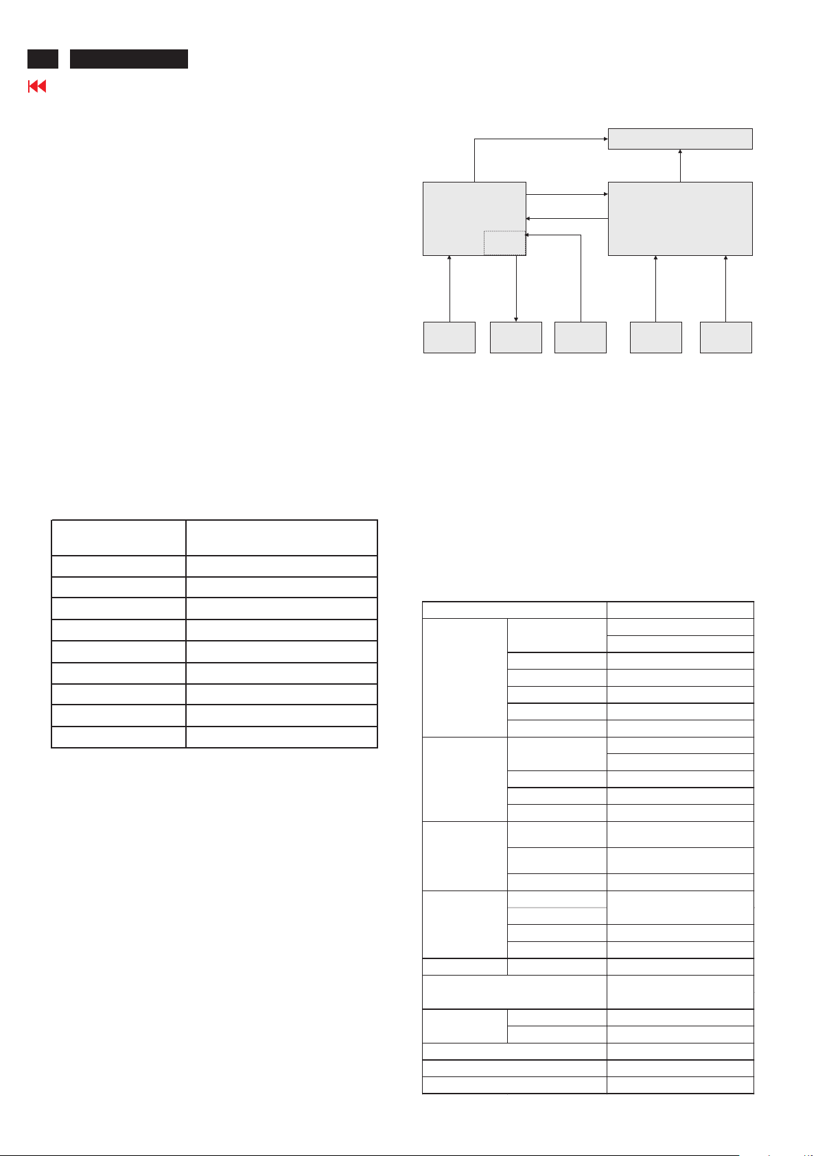
LCD Flat Panel
Interface Board
Flat Panel Controller,DDC
Power Board
AC to DC Adapter
DC to AC Inverter
Audio
AMP
(Option)
AC-IN
1W*2
Speaker
(Option)
Audio Source Host Computer
Function Key
Board
CCFL
Panel data & control. DC power
Speaker
line input
DC 5V
Audio line input
Video Signal input& DDC
Function key input
Display Area
21.5” diagonal
476.64mm(H)x268.11mm(V)
Resolution 1920 x 1080 pixels
Display Color Number 16.7M colors(6bit Hi FRC)
Display Type a-Si TFT active-matrix
Contrast Ratio 1000 : 1 typ.
Brightness 250cd/m2 typ.
Response Time (Ton + Toff) 5 ms typ.
Pixel Pitch 0.248mm(H) x 0.248mm(W)
Vertical Viewing 160 degrees typ, CR>10
Horizontal Viewing 170 degrees typ, CR>10
SPEC
H 31kHz ~ 82kHz
V 56Hz ~ 75Hz
Max Pixel clock 210MHz
Video input 0.7Vp-p
RGB Input Impedance 75Ù
Sync Input Signal Separate SYNC, Composite Sync
Sync Input Impedance 2.4KÙ(1A1D1H), 50Ù(1A1D/1A)
H 31kHz ~82kHz
V 56Hz ~ 75Hz
Max Pixel clock 165MHz
Input Level 150mV<=Vp-p<=1560mV
Input Impedance Input Impedance 100Ù per pair
AC power
AC 100V ~ AC 240V ± 10% 50/60Hz,
3 pin AC power cord
Input connectors
D-SUB 15pin, DVI-D 24pin, HDMI
19pin
Audio Jack ( OPTIONAL) Audio input 3.5Ö
AC IN 100~240V
Normal Operation
Power Saving < 1W
Power Off < 1W (90VAC~264VAC)
User’s Control Front Panel Buttons Right, Left, MENU, AUTO,E,Power
Preset Timing 13
User’s Timing 9
VESA DDC2B
VESA DPMS
H ±1kHz, V ±1 Hz
Pre-Defined Timing
Power Saving
Input Signal Counter tolerance
Plug and Play
Connectors
Power Consumption
30W Max(with audio)
35%typical, 65%min
Dimming control range
(max-min/max) x100%
ITEM
Frequency Ranges
Analog Signal Input
(VGA)
Digital Signal Input
(DVI&HDMI)
Frequency Ranges
ACER A211H/A221HQ
2
1. Product Specification
Go to contents page
This model combine with three platforms. See below
explanation.
1. Scaler IC: RTD2482D used in VGA, DVI and HDMI port.
Using simply word to define it.(1A1D1H)
2. Scaler IC: RTD2281 used in VGA and DVI port. Using simply
word to define it.(1A1D)
3. Scaler IC: RTD2280L used in VGA port. Using simply word to
define it.(1A)
1.1 Scope:
This document defines the design and performance
requirements for the 21.5” wide flat panel monitor. The
display elements shall be a 21.5” inch diagonal, UXGA
(1920 x1080) resolution TFT-LCD display .Video input
signals include D-sub and digital DVI-D , HDMI and
DP(DisplayPort) depends on different model. Power saving
function complies with the VESA DPMS (Display Power
Management Standard).
General display parameters:
This LCD monitor includes an interface board, a power
board and a function key board.
The interface board controls the TFT panel control logic,
brightness control logic, and DC-DC conversion to supply
the appropriate power to the whole board and LCD panel.
The LVDS signals transmit video data to LCD Module to
drive the LCD display circuit.
The power board will provide the DC power to the interface
board, LCD panel and inverter board.
The function key board is used for OSD control, monitor
power ON/OFF and the LED indicator for power status.
This monitor meets Energy Efficiency grade 2 of China.
1.2 General Requirements:
1.3 Electrical:
1.2.1 Test Condition:
Normal test condition is that brightness level set at
Max. and contrast level set default. Test pattern is full
white pattern. The warm up time is more than 30
minutes. Ambient light should be less than 1 Lux.
1.2.2 Test Equipment:
The reference signal source is a calibrated Chroma
2326 or Quantum 801GD video generator. The use of
compatible generators during qualification and
production is acceptable.
Luminance meter is Minolta CA210, TOPCON BM7 or
compatible equipment.
This section describes the electrical requirement of the
monitor. Below is the block diagram.
Page 5
1. (continued)Product Specification
Pin Signal Description
1 Red-Video Red video signal input
2 Green-Video Green video signal input
3 Blue-Video Blue video signal input
4 GND Ground
5 Self Test Detect VGA Cable have connected or not
6 Red-GND Analog signal ground for the Red video
7 Green-GND Analog signal ground for the Green video
8 Blue-GND Analog signal ground for the Blue video
9 + 5V
+5 input from host system for the VESA DDC2Bi
function
10 DDC-GND Signal ground
11 GND Ground
12 DDC-SDL
SDA signal input for the VESA
DDCB2i function
13 H-SYNC Horizontal signal input from host system
14 V-SYNC Vertical signal input from the host system
15 DDC-SCL SCL signal input for the VESA DDC2Bi function
PIN NO SYMBOL FUNCTION
1 RXOIN0- Negative LVDS differential data input(Odd Data)
2 RXOIN0+ Positive LVDS differential data input(Odd Data)
3 RXOIN1- Negative LVDS differential data input(Odd Data)
4 RXOIN1+ Positive LVDS differential data input(Odd Data)
5 RXOIN2-
Negative LVDS differential data input(Odd Data,
DSPTMG)
6 RXOIN2+
Positive LVDS differential data input(Odd Data,
DSPTMG)
7 GND Power Ground
8 RXOCLK- Nega tive Sampling Clock input (ODD clock)
9 RXOCLK+ Positive Sampling Clock input(ODD clock)
10 RXOIN3- Negative LVDS differential data input(Odd data)
11 RXOIN3+ Positive LVDS differential data input(Odd data)
12 RXEIN0- Negative LVDS differential data input(Even data)
13 RXEIN0+ Positive LVDS differential data input(Even data)
14 GND Power Ground
15 RXEIN1- Negative LVDS differential data input(Even data)
16 RXEIN1+ Positive LVDS differential data oinput(Even data)
17 GND Power Ground
18 RXEIN2- Negative LVDS differential data input(Even data)
19 RXEIN2+ Positive LVDS differential data input(Even data)
20 RXECLK- Negative Sampling clock input(Even clock)
21 RXECLK+ Positive Sampling clock input(Even clock)
22 RXEIN3- Negative LVDS differential data input(Even data)
23 RXEIN3+ Positive LVDS differential data input(Even data)
24 GND Power Ground
25 NC No connection(For AUO test only. Do not connect)
26 NC No connection(For AUO test only. Do not connect)
27 VDD
28 VDD
29 VDD
30 VDD
Power Supply: +5V
Pin Signal Pin Signal
1 TMDS Data 2+ 11 TMDS Clock Shield
2 TMDS Data 2 Shield 12 TMDS Clock-
3 TMDS Data 2- 13 CEC
4 TMDS Data 1+ 14 Reserved
5 TMDS Data 1 Shield 15 SCL
6 TMDS Data 1- 16 SDA
7 TMDS Data 0+ 17 DDC/CEC Ground
8 TMDS Data 0 Shield 18 +5V Power
9 TMDS Data 0- 19 Hot Plug Detect
10 TMDS Clock+
Pin Signal Pin Signal
1 TMDS Data 2- 13 NC
2 TMDS Data 2+ 14 +5V P OWE R
3 TMDS Data GND 15 Self Test
4 NC 16 Hot Plug Detect
5 NC 17 T MDS D ata 0-
6 DDC Clock 18 TMDS Data 0+
7 DDC Data 19 TMDS Data G ND
8 NC 20 NC
9 TMDS Data 1- 21 NC
10 T MDS Data 1+ 22 TMDS Clock GND
11 T MDS Data G ND 23 TMDS Clock +
12 NC 24 TMDS Clock -
ACER A211H/A221HQ
Go to contents page
3
1.3.1 Interface Connectors:
1.3.1.1 Power Connector and Cable:
The AC inlet connector shall be an IEC/CEE-22
type male power receptacle for connection to
mains power. The power cord shall be black/white
depending on the color of machine with length of
1.8±0.05 meters. The power cord type is different
from regions.
1.3.1.2 Analog Connector and Cable:
These signal input connector shall be 15 D-sub
capable of receiving VGA analog signal. The VGA
signal cable shall be black and with length of
1.8meter. The D-sub cable shall be a molded-
over, shielded, triple row, 15 pins and blue color D
type connector.
1.3.1.3 DVI-D digital Connector and Cable:
These signal input connector shall be 24 DVI-D
capable of receiving TMDS digital signal. The DVI
cable shall be black and with length of 1.8meter.
The DVI cable shall be a molded-over, shielded,
triple row, 24 pins, and white color DVI-D
connector.
1.31.4 HDMI digital video and audio Connector and
Cable:
These input connector shall be capable of
receiving digital video and audio signal per HDMI
requirement. The optional HDMI cable shall be
Connector Pin Assignment:
black and with length of 1.8 meter.
A. D-SUB
B. DVI-D (Digital TMDS) Connector
C. HDMI Connector
D. Flat Panel Connector
Page 6
LED Color
Power-ON Mode: Blue
Power Saving Mode: Amber
Shortcut menu Content OSD Display
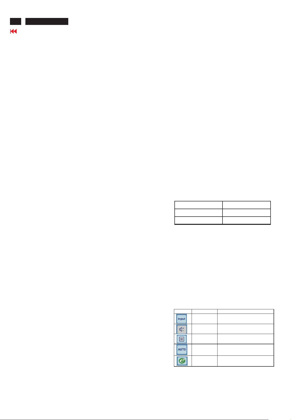
Input change function
Use Input key to select from different video
sources that may be conne cted to your monitor.
Speaker Volume
control function
Press this button to acti vate the Volume menu.
OSD Function Press this button to activate the OSD menu.
Auto Adjust Function
Press this button to acti vate the Auto Adjustment
function. The Auto Adjustment function is used
to set the HPos, VPos, Clock and Focus.
Empowering
Press the Empowering Key to open the Acer
eColor Management OSD and access the
scenario modes.
ACER A211H/A221HQ
4
Go to contents page
1. (continued)Product Specification
1.3.2 Input Signals:
1.3.2.1 Video Signal Amplitudes:
The video inputs consist of Red, Green and Blue
signals each has its own coaxial cable terminated
at the monitor. These video signals are analog
levels, where 0V corresponds to black, and
700mV is the maximum signal amplitude for the
respective color. The video signal is terminated
with 75 ohms.
1.3.2.2 Video Signal Termination Impedance:
The analog video signal termination shall be 75
ohm +/- 2%.
1.3.2.3 Synchronization (Sync) Signals:
The Horizontal Sync (HS) TTL signal is used to
initiate the display of a horizontal line. HS may be
either active high or active low according to the
timing. The Vertical Sync (VS) TTL signal is used
to initiate the display of a new frame. VS may be
either active high or active low according to the
timing.
1.3.2.4 Sync Signal Levels:
The monitor must accept sync signals from both
3.3 and 5 volt TTL logic families. The inputs shall
sense a logic 0 when the input is 0.8 volt or less
and shall sense a logic 1 when the input is 2.0
volts or greater. In addition to these level
requirements, there shall also be a minimum of
0.3 volt hysteresis provided for noise immunity
(typically by using a Schmitt Trigger input). That
is, the input level at which the monitor actually
detects a logic 0 shall be at least 0.3 volt lower
than the level at which it actually detects a logic 1.
If the monitor sync processing circuits were
designed with 3.3 volt logic family, then the sync
inputs must be 5 volt tolerant.
1.3.2.5 Sync Signal Loading:
TTL input loading shall be equivalent to one TTL
input load. When logic 0 is asserted by a sync
input, the maximum current source from any
single monitor sync input to the driver is 1.6 mA.
When logic 1 is asserted, the maximum current
source from the driver to any single monitor sync
input is 400 uA.
1.3.2.6 Abnormal Signal Immunity:
The monitor shall not be damaged by improper
sync timing, pulse duration, absence of sync,
abnormal input signal amplitude, or any other
anomalous behavior of a graphics card.
1.3.2.7 Digital TMDS Input (DVI and HDMI signal input):
These video inputs consist of TX0+/- to TX2+/-±
and CLK+/- signals, each with its own shielded
twisted pair. These video signals are digital levels.
Each signal pair is terminated by a normal 100
ohms.
1.3.2.8 Audio Function (optional):
This monitor integrated with stereo audio.
Speakers: 2 x 1W
Amplifier: Output 1W with 500mVrms Sine wave
input.
Input impedance: >22K Ohms.
THD: <10%.
1.3.3 User Controls and Indicators:
1.3.3.1 Power On/Off Switch:
The monitor shall have a power control switch
visible and accessible on the side of monitor.
1.3.3.2 Power Indicator LED:
The monitor shall have LED indicators located on
the front of the monitor. Table 1 is the LED color
for the power indicator.
1.3.3.3 On-Screen Display:
On Screen Display system shall be used to
control the monitor. Current setting will be saved
and OSD will be tuned off when the keys are not
touched for a period of time. (Please see OSD
timeout section)
A) Key Function Overview: All functions are
controlled by OSD buttons on the front cover.
Press the function button to open the shortcut
menu. The shortcut menu lets you quickly select
the most commonly accessed settings.
B) Menu Operation:
Pressing the MENU button brings up the first level
menu. This menu button is used to enter the
second OSD menu also.
Page 7
C) OSD Function:
Cabl e Remark
640x480p@59.94/60Hz 59.94/60Hz Cat1
720x480p@59.94/60Hz 59.94/60Hz Cat1
1280x720p@59.94/60Hz 59.94/60Hz Cat1
720x576p@50Hz 50Hz Cat1
1280x720p@50Hz 50Hz Cat1
1920x1080i@59.94/60Hz 59.94/60 Hz Cat1
1920x1080i@50Hz 50Hz Cat1
1920x1080p 50Hz Cat2
1920x1080p 59.94/60 Hz Cat2
Primary Video Format Timings
CEA
Timming
ITEM Content
Volume To increase or decrease the sound lev el
Brightness Adjust backlight luminance of the LCD panel
Contrast Adjust gain of R,G,B signal
Clock Adjust the ratio of dividing frequency of the dot clock
Focus Adjust the phase of the dot clock
H.Position The active screen is horizontally mo ve right and left
V.Position The active screen is vertically move up and down
Color temp Select three kinds of modes(Warm, Cool, User)
1.USA-select the language among En glish, French,
Italian, Deutsch, Spanish,
繁體中文, 簡體中文, 日本語
2.EMEA-select the language among English,
French,Italian , Deutsch, S panish, Russian, Dutch,
Finnish
OSD Position Adjust the OSD menu position
OSD Timeout The OSD menu show time
Setting The setting of Input Source, Wi de Mode, DDC/CI
Information
It will show resolution, the frequency of
horizontal/vertical synchronizing and S/N
Reset All data copy from shipment factory data
OSD
Language
Power
Saving Mode
Menu
This func ti on gives a warning m ess age when selected input
signal is n ot active. When the M on itor dete cted that the VGA
or DVI is su spend or standby mo de. The M onitor shall display
a messag e, “No Signal” for 4 s econd s an d the LE D shall be
blue, and to alert the user t ha t input signal is not a ctive.
Then the m onitor sha ll go into sleep mode a nd the LED shall
be Amber.
Out of
range Menu
This func ti on gives warning me ssage about input reso lution or
refresh rate that the mo nitor cannot support . W hen an inp ut
signal wh ich is out o f t he normal operat ion range define d in
Section 3 .2. Then the monitor w ill display “Input not supported”
message :
1. Pixel c lock frequency : Fc>165 (Digital)
Fc>205 (Analog)
2. V-syn c frequency: 50Hz>FV >=76Hz
3. H-sy nc f requ en cy: 30KHz>FH>83K Hz(Analog );
30KHz>FH>8 3KHz(Dig ital)
Check Signal
cable Menu
This func ti on gives warning me ssage when the VGA ca ble is
not connecte d. When the Monitor de tected that the VG A ca ble
is not conn ecte d to the mon itor. The OS D s ha ll display a
message “Cable not connected” all the time to alert the user
that the vide o cable is not plugge d in. The LED shall b e blue.
The moni tor s hall use a method of a pull-up resistor o n a
ground pi n t o determine if the vide o ca ble is connected to
the PC.
Resolution Horizontal Vertical Nominal Pixel User Manual
(active dot)
Frequency
(KHz)
Frequency
(Hz)
Clock (MHz) de scription
640x480@60Hz 31.469 59.941 25.175 Yes Established Timing
640x480@72Hz 37.861 72.809 31.5 No N/A
640x480@66.66Hz 35 66 .6 6 30.24 Yes Established Timing
720x400@70Hz 31.469 70.087 28.322 Yes Established Timing
800x600@56Hz 35.156 56.25 36 Yes Established Timing
800x600@60Hz 37.879 60.317 40 Yes Established Timing
800x600@72Hz 48.077 72.188 50 No N/A
1024x600@60Hz 37.32 60 48.964 No N/A
1024x768@60Hz 48.363 60.004 65 Yes Established Timing
1024x768@70Hz 56.476 70.069 75 Yes Established Timing
1152x864@75Hz 67.5 75 108 Y es Standard Timing
1280x960@60Hz 60 60 108 No N/A
1280x1024@60Hz 63.981 60.02 108 Yes Standard Timing
1280x720@60Hz 44.76 60 74.481
No N/A
1280x800@60Hz 49.702 59 .8 1 83.5
Yes Standard Timing
1360x768@60Hz 47.712 60.015 85.5
No N/A
1440x900@60Hz 55.935 59.887 106.5 Y es Standard Timing
1680x1050@60Hz 65.29 59.9 54 146.25 No N/A
1600x1200@60Hz 75 60 162 No N/A
1920x1080@60Hz 67.158 59.963 173 Yes Standard Timing
1920x1080@60Hz 67.5 60 148.5 Yes Detail timing
1920x1080@60Hz 66.587 59.934 138.5 No
EDID
1. Product Specification (continued)
monitor shall display a warning screen indicating
that the input frequency is out of range. Under no
circumstances shall any combination of input
signals cause any damage to the monitor.
1.3.4.2 Factory Assigned Display Modes:
There are 13 factory pre-set video modes. Pre-
defined mode parameters will be recalled if the
operating mode is one of those pre-set modes. If
the operating mode is not one of those stored in
memory, the monitor CPU will select the PRESET
timing for a mode that is the next lowest in
horizontal scanning frequency The screen
parameters can be adjusted by the front bezel
control buttons and then saved as a user defined
mode. The monitor shall include all the preset
video timings shown in the following page.
Preset Timing Chart:
ACER A211H/A221HQ
Go to contents page
5
D) OSD Control Factory Default Values:
The OSD controls shall have the following factory
default values:
Brightness: 77
Contrast: 50
Color Temperature:
Warm(6500)/Cool(9300)/User (R/G/B all are 100)
1.3.4 Monitor Modes and Timing Capability:
1.3.4.1 Format and Timing:
Horizontal Position of Screen: 50
Vertical Position: 50
OSD Time: 10 seconds
OSD Language: English
The monitor shall synchronize with any vertical
frequency from 55 to 76 Hz, and with any
horizontal frequency from 30 to 83 KHz for analog
input and from 30 to 83 Khz for DVI input. If the
input frequency is beyond the specified range, the
Preset video timings (digital inputs)
1.3.4.3 Mode Recognition Pull-in:
The monitor shall recognize preset modes within
a range of +/- 1 KHz for horizontal and within a
range of +/- 1Hz for vertical.
1.3.5 Controller Requirements:
1.3.5.1 General Requirements:
The monitor shall include a controller which is
capable of converting the analog RGB signal or
Page 8
Input Voltage Ra nge
The operatin g range shall be from 90 to 264 VA sinusoi dal for all
models spe cified.
Input Frequency Ra nge Inp ut power frequ ency range shall be from 47 to 63Hz.
Power Con sumption
Power consu mption for the monitor shall be less than 30W ove r
the specified voltage an d frequency ranges. In powe r off mode the
power con sumption will be less than 1W (at 90VAC~26 4VAC).
Line Fuse
The AC input shal l be fused and become el ectrically open as a
result on an un safe current level. The fuse may not be user
replace able.
Initial Co ld Start
The power sup ply shall start and function pro perly when unde r full
load, with w orst case condi tions of inpu t voltage, inp ut frequency,
operatin g tempera ture, and cold backlig ht lamps.
Inrush Curren t
The inrush curre nt must be limited to 35A when operated at
120VAC, and 80A when operated at 220VAC. In - rush current is
measured at an ambien t temperature of 25° C, with the uni t
temperature stabi lized in the powe r - off.
Hot Start Cycle
The power sup ply shall not be damag ed when switched ON
for one second and OFF for one second for seven
consecutive times after operating for one hou r at full load ,
25°C, and nomina l input line voltag e.
Under Vol tage
The power sup ply shall contain pro tection circui try such that
the appl ication of an input voltage below the minimum
specified in this table shall no t cause damag e to the power
supply un it nor cause fail ure of the input.
Line Transi ent
The power sup ply shall operate wi thin IEC 801 -4 (+/-1KV)
and IEC 801 -5 (+/-2KV) for the dome stic U.S. Version. The
UPS power sup ply shall operate an d comply with CE mark.
DC Output 5 .15+/-0.2V (1.85A); 22+/-2V (0.75 A)
Item Min. Typ. Max. Unit
Output Curre nt 3 7.5 8 mArms
Output Voltage
7 91
Vrms
Operation frequency 40 5 5 60 KHz
Striking Voltage --- --- 1780 Vrms
Inverter specification for M215HW01 V7
ACER A211H/A221HQ
6
1. Product Specification (continued)
Go to contents page
DVI digital signal to the panel. The controller will
include a PLL, A/D converters, TMDS receiver
and other circuitry necessary to perform its
function. The PLL shall be stable enough to
ensure a stable image.
1.3.5.2 Video Stretching:
The monitor shall have the function to “stretch”
the video signal, so that an input signal from the
computer in any resolution smaller than 1920 x
1080 is automatically expanded to fill the entire
screen.
1.3.5.3 Panel Timing and Interface:
The controller supplied with the monitor shall
control all panel timing. This controller shall
adequately insulate themonitor from the
computer, so that no possible combination of
input signals from the computer shall cause
damage to the flat panel or any other component
of the monitor.
1.3.6 DC - AC Inverter Requirements:
The frequencies used by the DC - AC inverter should be
carefully selected to prevent any noticeable effects on the
screen (such as a rolling effect). The Inverter
specification detail information in Table 2:
1.3.7 Power Supply Requirements:
The AC to DC power supply for this monitor shall be an
integrated power supply. This power supply shall have an
IEC receptacle for mains power input and provide
sufficient power for backlight assembly, interface board
and panel. And it should meet all requirements specified
in the following Table.
1.3.8 Display Communications Channel:
The monitor shall provide a display communications
channel that conforms to VESA DDC2B hardware
requirements. This configuration shall contain the
128-byte EDID file as specified by VESA E-EDID
Standard. Once the EDID is programmed the write
protection function will enabled. So the EEPROM
data cannot be overwritten.
1.4 Flat Panel:
1.4.1 General Requirements:
The panel shall be a Full HD resolution 21.5”
diagonal TFT-LCD.
1.4.2 Panel Timings:
The controller in the monitor shall translate video
timings from the PC to meet the timing requirements
listed in Panel specification. Under no circumstances
may the controller supply the panel with timings that
may result in damage. The controller shall insulate
the panel from the PC, so that the panel shall always
be driven according to its specification regardless of
the timings being sent from the PC.
1.4.3 Polarizer Hardness:
The outer face of the front polarizer panel shall be
covered with a coating with a 3H hardness value.
1.4.4 Backlight Requirements:
The backlight assembly shall be designed to support
field replacement at the customer site or authorized
service center. The backlight module shall have a
continuous operating life of at least 30,000 hours at
25°C. The operating life is defined as having ended
when the illumination of light has reached 50% of the
initial value. The backlight module shall extend a
sufficient amount from the edge of the light guide that
sputtering over the life of the
backlight shall not cause degradation of the
luminance uniformity (such as non-illuminated bands
along the edges of the display).
Page 9

1. Product Specification (continued)
ACER A211H/A221HQ
Go to contents page
7
1.4.5 Defects:
1.4.5.1 Visual Inspection:
The LCD panel shall be inspected with all pixels
set to white, black, red, green and blue. The color
variation, brightness variation, and overall
appearance must meet the SPEC.
1.4.5.2 Display Degradation:
Over the life of the product, variation of the
parameters specified in Panel specification shall
be maintained within reasonable limits. The panel
must not exhibit any significant defects while in
operation (excluding the lamp operation).
This does not in any way change the warranty
given by the panel manufacturer.
1.4.5.3 Light Leakage:
Except for the active display area, there shall be
no light emission visible from any angle from any
other part of the display. For this test, the ambient
illumination will follow the panel specification 300
to 700 lux.
1.4.5.4 Allowable Defects:
No cosmetic defects are allowed except those
specified below. The conditions of visual
inspections are as follows:
- Viewing distance: 35 ~ 50cm.
- Ambient illumination: 300 to 700 lux.
- Viewing angle shall be at 90 degree.
- Defects not apparent within one minute shall be
ignored.
1.4.5.5 Defect Terminology:
The following gives the descriptive terms used in
classifying defects
Dark Spots / Lines:
Spots or lines that appear dark in the display
patterns and are usually the result of
contamination. Defects do not vary in size or
intensity (contrast) when contrast voltage is
varied. Contrast variation can be achieved
through the use of varying gray shade patterns.
Bright Spots / Lines:
Spots or lines that appears light in the display
patterns. Defects do not vary in size or intensity
(contrast) when contrast voltage is varied.
Contrast variation can be achieved through the
use of varying gray shade patterns.
Polarizer Scratch:
When the unit lights, lines appear light (white)
with display patterns dark and do not vary in size.
Physical damage to the polarizer does not damage the
glass.
Polarizer Dent:
When the unit lights, spots appear light (white) with
display patterns dark and do not vary in size. Physical
damage to the polarizer does not damage the glass.
Rubbing Line:
Horizontal or diagonal lines that appear gray with the
display patterns dark and may have resulted from an
“out of control” rubbing process on the polyimide or
“waves” on the BEFs or prism sheets .
Newton Ring:
The “rainbow“ effect caused by non-uniform cell
thickness.
Mottling:
When the unit lights, variation / non - uniformity(splotch)
appears light (white) with the display and might vary in
size.
Dim Line:
When the unit lights, line(s) in the minor (vertical) or
major (horizontal) axis appear dim, but not completely
on or off.
Cross Lines Off:
When the unit lights , lines in both the minor and major
axis do not appear.
Bright/Dark Dot:
A sub - pixel (R, G, B dot) stuck off / on (electrical).
1.4.5.6 Smudges, Streaks and Smears:
When viewing the panel oriented so as to maximize
reflected light, there shall be no visible smudging,
streaking, smearing or other non-uniformity from
contaminants, fingerprints, or defects in any of the
visible surfaces. This is independent of whether the unit
is operating or off.
1.4.5.7 Other Defects:
Undefined defects that are considered to be rejectable
by Acer will be reviewed by Wistron as they become
apparent. These panels will be referred to the Wistron
Corporate / Manufacturer Purchasing Agreement for
disposition
1.4.5.8 LCD Inspection:
Put LCD panel on inspection table and illuminate the
panel with a daylight fluorescent lamp located above the
panel surface such that the luminance at the LCD panel
is between 1000 lux. and 1500 lux. Defect limits are
given inTable 4 .
Page 10
Average Dia meter
Smaller of (L+W)/2 or
L/20 + 2W
Acce ptable
Number
Minimum Sep aration
< 0.1mm Non coun table N / A
0.1mm - 0.3mm 10 15mm
0.31mm - 0.5mm 10 15mm
0.51mm - 1.2 5m m 5 15mm
1.26mm - 2.5mm 3 25.4mm
2.51mm - 0.3mm 3 25.4mm
Greater than 3.75mm None No t applicable
Table 4. Desc ript iv e Terms
ACER A211H/A221HQ
8
1. Product Specification (continued)
Go to contents page
Allowable distance between spots of two sizes is the
minimum separation number for the smaller spot.
Therefore, if there are two spots, 1.30 mm and 0.4
mm in diameter, they must be at least 15 mm apart.
1.5 Optical Characteristics:
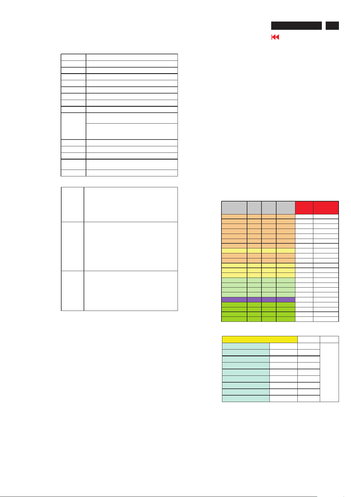
1.5.1 Brightness uniformity:
The uniformity is determined by using a photometer
(CA-210) to measure the 9 points luminance in front
of monitor after at least 30 minutes warm up. It shall
be test at 1920x1080/60Hz mode and full white
square pattern with contrast / brightness in default
value. The values specified are at an approximate
distance 20 cm from the LCD surface and at 0
viewing angle.
The 9 test points are defined as below:
1.5.2 Contrast ratio (CR) :
1.5.2.1 General CR:
The contrast ratio is determined by using a photometer
(CA-210) to measure the maximum and minimum
luminance in front of monitor after at least 30 minutes
warm up. It shall be test at 1920x1080/60Hz mode
and full white/full black square pattern with
contrast/brightness in default value. The values
specified are at an approximate distance 20 cm from
the LCD surface and at 0 viewing angle.
The contrast ratio is calculated as below:
CR=(Max. full white luminance)/(Max. full black
luminance)
CR = 600:1(min.), CR=1000:1(typ.)
1.5.2.2 ACM (Auto Contrast Management):
The input image signal source may be various levels
of illumination, and this ACM unit can analyze it as
histogram for the various levels of illumination,
according to the analyzed result, when input a low-
luminance level image, display brightness will be
adopted to corresponding low level, so that enhance
the contrast rate, this facilitates visual ergonomics
enhancement .
The monitor should me CR >50000:1 when ACM
function is active.
1.5.3 Response time:
The response time is defined as below:
The brightness uniformity is calculated as below:
Brightness uniformity >= 75%
Remark: The black luminance non-uniformity are no
defined by panel spec, therefore, we don't define the
spec. for black luminance non-uniformity.
Tr + Tf : 5 msec typ.
Remark: Optical response time vs gray scale.Test
condition: brightness set to max, and contrast set to
default.
1.5.4 Viewing angles:
The viewing angles are measured at CR >=10 as below :
Page 11
1. Product Specification (continued)
Height (including stand) 370mm
Depth (including stand) 161 mm /52.5mm(without base cover)
Width 511.3mm
Pack Dimensions (H x W x L) 570L)x114(W)x396(H)mm
Packaged Weight 4.95kg
Unpacked Unit Weight 3.49 kg
40” container loading, palletized 2000 units
Maximum Stacking Height 5 layers, 2103 mm
Mounting Method 100 x 100 mm VESA Mount
Attachment Method (4) Screws ,M4 x 10mm flat head Phillips socket
Tilt Range -5+/-1.5 degree, +15+/-1.5 degree
Swivel Range -0degree, +0 degree
Lift Range 0mm
Pivot NO 0degree, clockwise
Stand base(attached or
detached for shipping)
detached
Stand Tilt/Swivel/Lift/Torque Backward
Tilt
Backward: 1.4+/-0.3 kgf Back ward(pivot): 0kgf
Forward: 1.4+/-0.3 kgf Forward(pivot): 0 kgf
3000 times still within spec
Swivel 0kgf/3500 times still with spec
Upward: 0 kgf/3500 times still within spec
Downward: 0kgf/3500 times still within spec
Pivot 0kgf/3500 times still within spec
Head Unit Squareness
|A-B|<= 5.0mm |C-D| <= 5.0mm
Head Unit Stability (Wobble
Resistance)
Time <= 5 seconds, Displacement <= 7 mm
Cable Management No
Kensington lock hole Yes
Normal Temperature Drop
Height (Packaged)
760 mm, 30 inches
Cold Drop Height (Packaged)
Sequence 1 corner ( Corner: corner2-3-5) -> 3 edges -> 6 sides
Lift
Horizontal Left: 85 degrees typ.
Right: 85 degrees typ.
Vertical Up: 80 degrees typ.
Down: 80 degrees typ.
1.5.5 Chromaticity:
The color chromaticity is measured by a photometer
(CA-210) at 1920x1080/60Hz mode and full white
square pattern with contrast/brightness in default
value. The x and y co-ordinates for Reddish, Bluish
and User preset mode shall be as below:
Reddish Preset (6500K):
x=0.313 +/- 0.020
y=0.329 +/- 0.020
Bluish Preset (9300K):
x=0.283 +/- 0.020
y=0.297 +/- 0.020
1.5.6 Brightness:
The uniformity is determined by using a photometer
(CA-210) to measure luminance on the center of
screen after at least 30 minutes warm up. It shall be
test at 1920x1080/60Hz mode and the brightness and
contrast OSD setting for 100%. The values specified
are at an approximate distance 20 cm from the LCD
surface and at 0 viewing angle. The full screen white
center luminance at User mode color temperature
shall be 250 cd/m² typ. And > 200 cd/m² min. Full
screen black pattern luminance at center should be <
1cd/m².
1.6 Environmental Requirements:
1.6.1 Temperature Ranges:
Operating Temperature: 5°C to 35°C
Shipping Temperature: -20°C to 60°C
1.7 Mechanical Specification:
Storage Temperature: -20°C to 60°C
1.6.2 Humidity:
Operating (non-condensing): 5% to 90%
Shipping (non-condensing): 5% to 90%
Storage (non-condensing): 5% to 90%
1.6.3 Altitude:
Operating 0 to +12,000 feet [3,658m].
Equivalent to 14.7 to 10.1 psia.
Shipping (Non-Operating) 0 to +40,000 feet
[12,192m].
Equivalent to 14.7 to 4.4 psia.
1.7.1 Mechanical Summary Table:
ACER A211H/A221HQ
Go to contents page
1.7.2 Stand:
1.7.3 Dimension(cm):
unit: mm
1.8 SHIPPING AND PACKING:
Packaging and wrapping shall be sufficient to protect the
product against damage or loss during shipment from the
supplier to the destination specified in the purchase order.
All packaging materials are subject to be tested and
evaluated. The container loading is 2000sets/40'.
The outside dimension of carton box is
570(L)x114(W)x396(H)mm.
9
Page 12
Key Func tion Description
Power Power on/off the monit or
A
Move the focus dow n
B Move the focus up
C
Enter to the it em page
(It has no fu nct ion at the information page)
D Exit the OSD menu
E Trigger the Acer eColor Ma nagement
Key Func tion Des cript ion
Power Power on/off the monit or
A Move the focus down
B Move the focus up
C Select function item for adjus tm ent
D Exit from the it em page t o ic on place
E Trigger the Acer eColor Ma nagement
Key Func tion Des cription
Power Power on/off t he monitor
A Increase the set ting value for target item
B Descrease the se tting vallue fo r target it em
C No function
D Exit from item selected status
E Trigger the Acer eColor Management
Key Function Desc ription
Power Pow er o n/off monitor
A Input Sw itc h
B Volume Mana gement OSD
C M ain M enu OSD
D Aut o C onfig
E Trigger the Acer eColor Management
10
ACER A211H/A221HQ
Go to contents page
2. OSD Menu
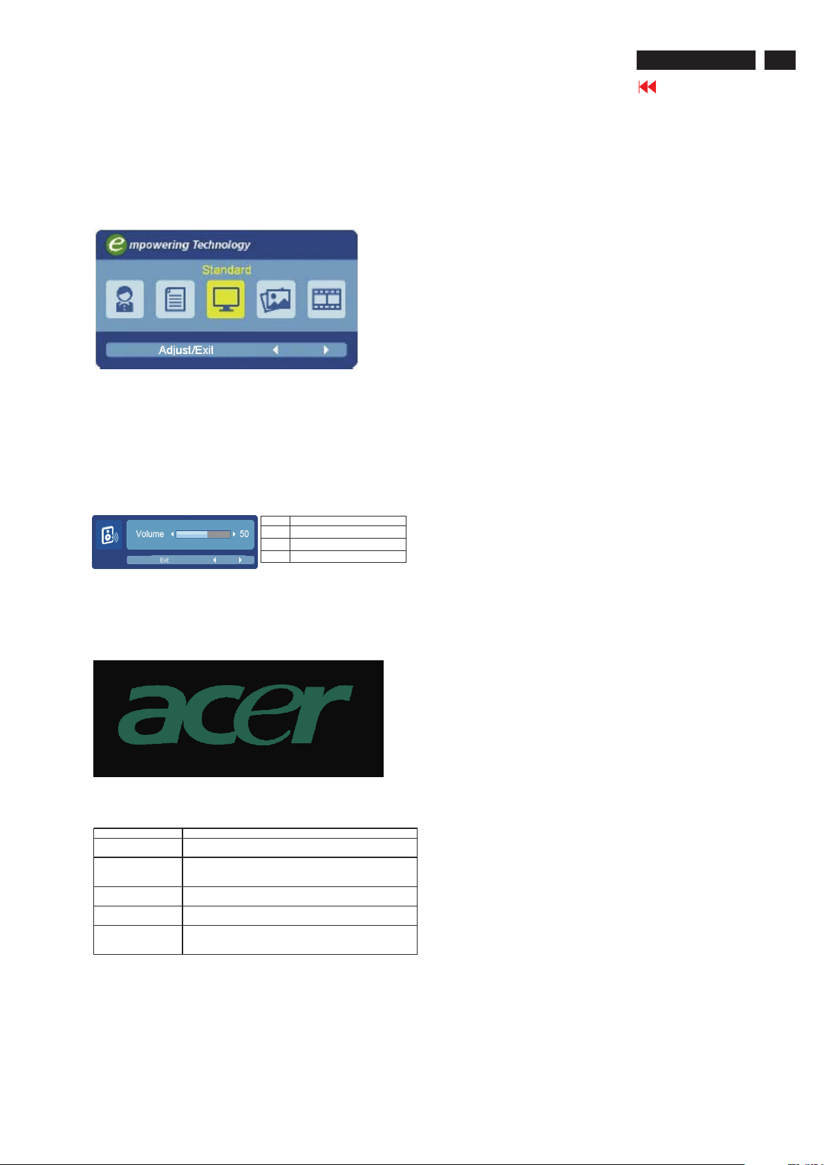
2.1 Function Menu:
1). Display Function Menu while user press any function
button.
2). Layout as following figure:
2.2 Key Definition:
C
DE
Power
AB
2.3 Main OSD Menu:
2.3.1. OSD layout:
1). Display OSD menu when user press “C” button in
Function Menu.
2). Layout as following figure.
Acer logo
b. Icons introduction
Function
Status
Non-Focus
Picture OSD Setup Information
Focus
Focus on
Item-page
c. Item page status
Status Display type
Non-focus
Item focused
Item selected
2.3.2 Key operation:
a. Key operation at function icon.
Funct ion Icon s
Information Bar
OSD layout for main menu
a. OSD layout for each function page
Picture OSD
Item page for
each function
group
Focus at main icons
b. Key operation at items page, no item selected.
Focus at item page
c. Key operation at items page, item selected.
1280x9 60
H:60KH z
S/N:ETLH10W004010 0BBE24300
Settings Information
Item is selected
Page 13
2. OSD Menu (continued)
Item Description
Auto Config Please Wait
When user press hot key "Auto" will show this messag e,
and the monitor do t he Auto config function.
Input Not Sup port
When the Hsync F requency,
Vsync Frequenc y or Resolution is o ut of the monitor suppo rt range,
will show this message. The message will be flying.
Cable Not Connecte d
When the video c ab le is not connected, will show thi s message.
This message will be flying.
No Signal
When the video c ab le is connected, but there is
no active signal input, w ill show this message,then ent er power saving.
Please Wait
After user trigger th e reset function,
system will show this messa ge notice user the reset is in proceeding.
2.4 Acer eColor management:
a. Display Acer eColor management OSD when user
press “e” button at Function menu or trigger this
function in OSD menu/picture page.
b. Layout as following figure.
OSD layout for the acer eColor management
2.5 Volume management OSD:
a. Display volume management OSD, when user press “<”
or “>” button on the front bezel.
b. Layout as following figure, key operation at items page.
(No item selected)
ACER A211H/A221HQ
Go to contents page
11
Key Function Description
A Volume up
B Volume down
D Close the Volume OSD
OSD layout for volume management
2.6 Acer logo:
When the monitor is turned on, the LOGO will be showed
in the center.
Acer logo
2.7 OSD Message:
Page 14

12
ACER A211H/A221HQ
Go to contents page
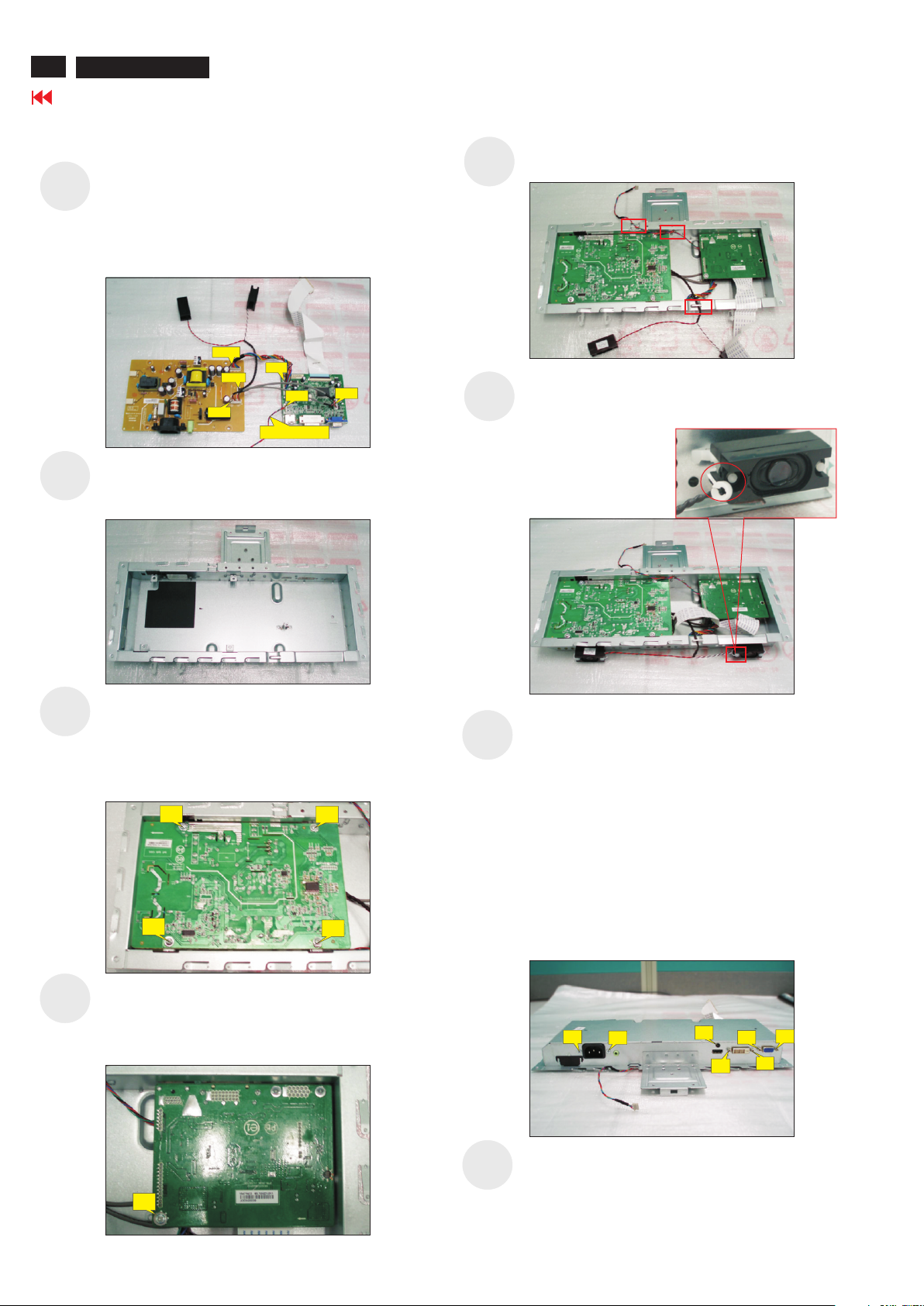
3.1 Pro duct Explo ded Diagra m:
3. Exploded Diagram
Page 15
3.2 Pac king Explo ded Diagra m:
3. Exploded Diagram (continued)
ACER A211H/A221HQ
Go to contents page
13
Page 16
14
ACER A211H/A221HQ
Go to contents page
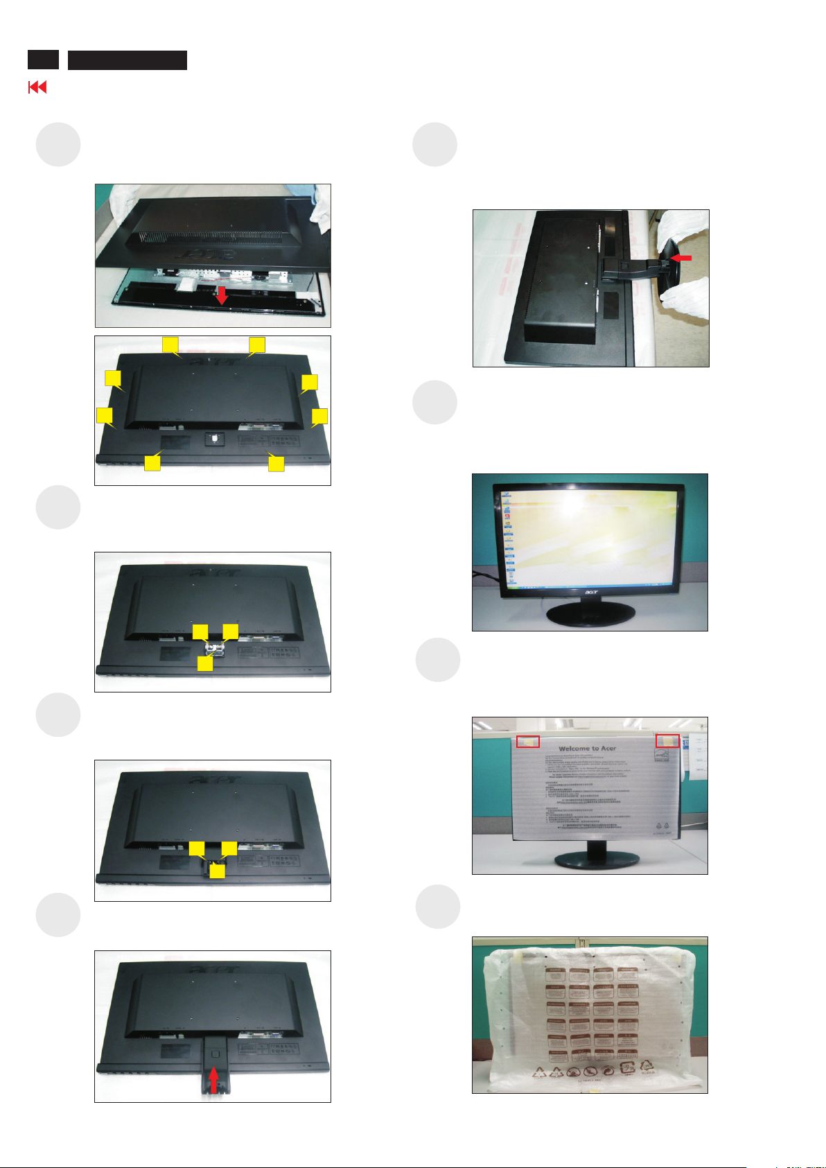
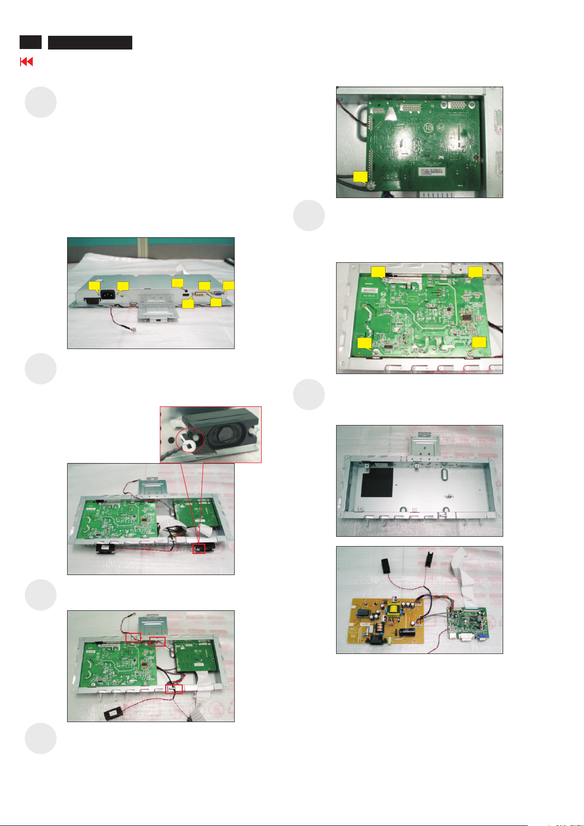
4. Assembly and Disassembly Procedures
4.1 Assembly procedures:
S1
Connect of power board with P301 of
interface board. Connect P003 of power board with
P802
P308 of interface board. Connect function key cable
with P309 of interface board. Connect the speakers’
cable to P001 of power board.
speaker’s cab le
Place a bracket chassis base on a protective
S2
cushion. Turn over the circuit boards and put them
into the bracket chassis base.
P802
P003
P001
LVDS Cable
P301
P309
funct ion key ca ble
P308
S5
Locate the function cable and audio cable in
the hooks shown as photo.
funct ion key ca ble
key
audio cable
Fix two speakers on the probes of speaker
S6
holders with caps.
S3
S4
Use a Phillips-head screwdriver to tighten four
screws till the power board and bracket chassis
base be firmly attached.
(No.1 screw size=M4x8, Torque=6~8kgfxcm;
No.2~4 screw size=M3x6, Torque=6~8kgfxcm)
1
3
4
2
Use a Phillips-head screwdriver to tighten one
screw till the interface board and the bracket
chassis base be firmly attached.
(No.1 screw size=M3x6, Torque=6~8kgfxcm)
S7
Turn over the bracket chassis module. Use a Hex-
head screwdriver to tighten four screws for locking
the DVI and D-Sub connectors.
(No.1~4 screw size=M3x8, Torque=5±1kgfxcm)
Use a
Phillips-head screwdriver to tighten one
screw for locking the HDMI or DP connector.
(No.5 screw size=M3x8, Torque=5±1kgfxcm)
Use a
Phillips-head screwdriver to tighten two
screws for locking the AC power outlet.
(No.6~7 screw size=M3x10, Torque=5±1kgfxcm)
7
6
5
4
1
2
3
Panel preparation: Examine the panel surface
S8
1
according to inspection criteria. Turn over the
panel to place the screen faced down for later
assembleing.
Page 17
4. Assembly and Disassembly Procedures (continued)
function key board
Plug lamp cables to the connectors of power
S11
board, then fix the lamp cables with tapes.
ACER A211H/A221HQ
Go to contents page
15
S9
Put the bracket chassis module on the back of
LCD panel module.
S12
S13
Place a front bezel on a protective cushion the
bracket chassis module into the front bezel. Adjust
the position of bracket chassis module till it is firmly
attached to the front bezel.
Take a function key board, then connect the
function key cable with the function key board.
Locate the function board in the hook of the front
bezel, then fix the function key cable with PVC
tapes.
, put
S10
Connect FFC cable to LVDS connector, fix the
cable with double faced adhesive tape which is
sticked on the back of cable.
function key board
Page 18
16
ACER A211H/A221HQ
Go to contents page
4. Assembly and Disassembly Procedures (continued)
S14
S15
Put a rear cover on the assembled unit and push
the rear cover on the positions marked as No.1~4 in
priority order for mechanisms engagement.
4
3
2
1
Use a Phillips-head screwdriver to tighten three
screws for fixing hinge with the rear cover.
(No.1~3 )Screw size=M4x9, Torque=12±1kgfxcm
4
3
2
1
S18
S19
Assemble. the hinge covers as the below picture.
Align the base cover with the stand and push the
base cover towards the top of the monitor for
assembling the base
Lift up the LCD module, check the acer logo if it is
firmly attached to the front bezel, connect a video
cable and power cord with the monitor and turn on
the monitor for functionality check.
S16
S17
1
2
3
Use a Phillips-head screwdriver to tighten three
screws for fix hinge cover with the hinge.
(No.4 )~6 Screw size=M4x8; Torque=6-7kgfxcm
4
5
6
Take a arm, then install the arm to the hinge cover
following the direction as the picture below.
S20
S21
Turn off the monitor and remove the video cable
and power cord from the monitor. Stick a screen
protector on the front bezel with adhesive tapes.
Take a EPE bag to cover the LCD monitor, put the
monitor face down on the table.
Page 19
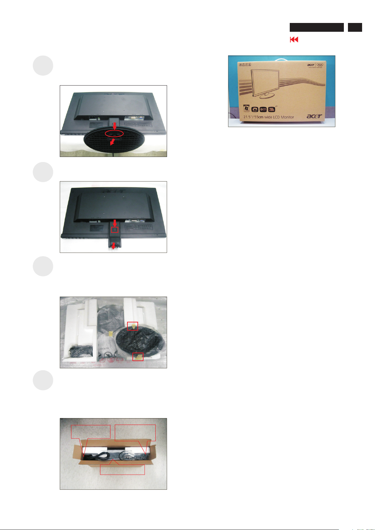
S22
S23
4. Assembly and Disassembly Procedures (continued)
Depress the release hook as indicated first before
removing the base and follow the arrow direction
to remove it.
Depress the release button as indicated, then
remove the arm follow the arrow direction.
ACER A211H/A221HQ
Go to contents page
17
S24
S25
Pack with PE bags. Take two
the base and arm
cushion foams to hold the LCD monitor, put the
base and arm on the specific positions as the
below picture. Fix the base with adhesive tapes.
base
arm
Move the whole unit into a carton and put
accessories including user’s manual, D-Sub
cable, audio cable, DVI cable, power cable and
UK cable on specific positions as the photo below.
Seal the carton.
POWER CABLE
DVI CABLE
UK CABLE
AUDIO CABLE
D-SUB CABLE
USER’S MANUAL
Page 20
ACER A211H/A221HQ
18
4. Assembly and Disassembly Procedures (continued)
Go to contents page
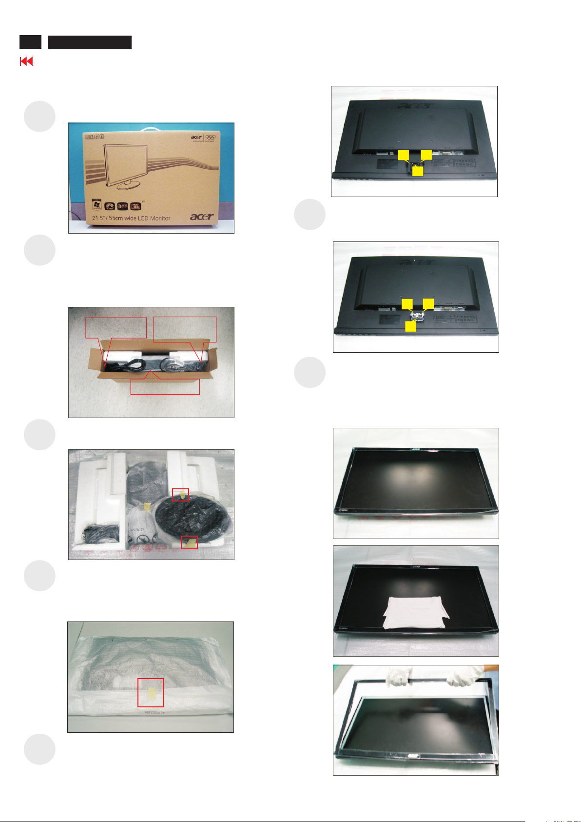
4.2 Disassembly procedures:
Open the carton with a proper tool.
S1
Take out all accessories including user’s manual,
S2
power cable, D-Sub cable, DVI cable, audio cable
and other packing materials from the carton.
(Note: It depends on whether users return the
accessories.)
1
3
2
Use a Phillips-head screwdriver to remove three
S6
(No.4~6 screw size=M4x9, Torque=11~13kgfxcm)
screws for releasing hinge.
5
6
POWER CABLE
DVI CABLE
Take out the whole cushion foams from the carton
S3
S4
and remove base and arm.
arm
Remove two cushion foams, tear off the adhesive
tape, take out the LCD monitor from the EPE bag,
remove the screen protector, then put the LCD
monitor on a protective cushion.
UK CABLE
AUDIO CABLE
D-SUB CABLE
USER’S MANUAL
base
S7
4
Turn over the LCD monitor to let the screen faced
up. Place a cloth on the panel where you are
working on to protect the panel. Then wedge your
fingers between the front bezel and the panel for
unlocking the mechanisms.
S5
Use a Phillips-head screwdriver to remove three
screws for releasing the hinge cover.
(No.1 Screw size=M4x8; Torque=6-7kgfxcm)
Page 21
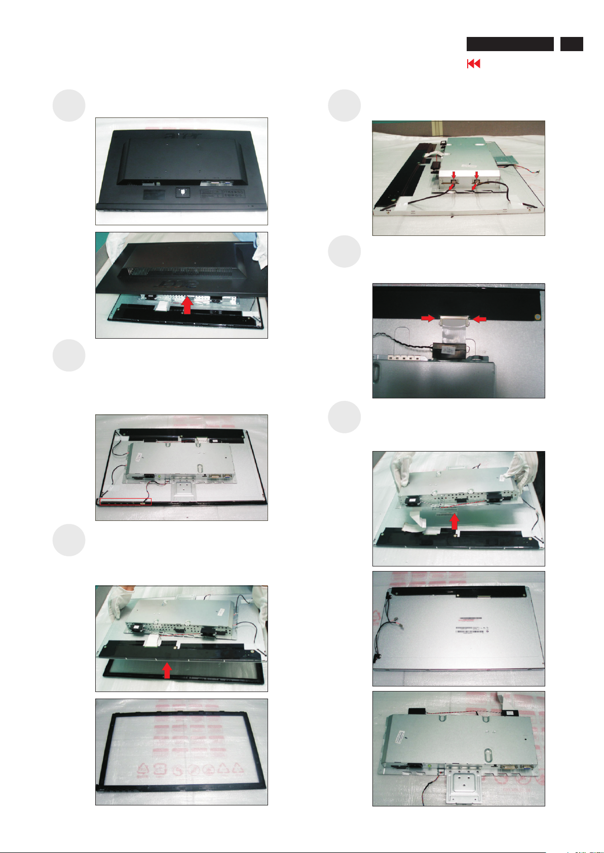
4. Assembly and Disassembly Procedures (continued)
function key board
ACER A211H/A221HQ
Go to contents page
19
Turn over the LCD monitor to let the screen faced
S8
Tear off the PVC tape,
S9
down and then remove the rear cover.
release the function key
board from the hook of the front bezel, then
disconnect the function key cable from
connector of the function key board
function key board aside.
the
. Put the
Unplug lamp cables follow the direction as the
S11
S12
Lift up the bracket chassis module for taking
S13
below picture.
Move the bracket chassis module down, push the
earing-lock, then remove the FFC cable from the
LVDS connector.
away the panel module, then put the bracket
chassis module on a protective cushion .
Lift up the bracket chassis module for removing the
S10
front bezel and then put the bracket chassis module
on a working table with protective cushion for later
disassembly.
Page 22
20
ACER A211H/A221HQ
Go to contents page
Use a Hex-head screwdriver to remove 4 screws for
S14
unlocking the DVI and D-SUB
connectors.
(No.1~4 screw size=M3x8, Torque=5±1kgfxcm)
Use a Phillips-head screwdriver to remove one
screw for unlocking the HDMI or DP connector.
(No.5 screw size=M3x8, Torque=5±1kgfxcm)
Use a Phillips-head screwdriver to remove two
screws for unlocking the AC power outlet.
(No.6~7 screw size=M3x10, Torque=5±1kgfxcm)
mechanisms of
4. Assembly and Disassembly Procedures (continued)
1
Use a Phillips-head screwdriver to remove four
S18
screws for unlocking the power board.
(No.1 screw size=M4x8, Torque=6~8kgfxcm;
No.2~4 screw size=M3x6, Torque=6~8kgfxcm)
S15
7
6
5
4
1
2
3
Turn over the bracket chassis module, and then
remove both of the speakers from the bracket
chassis module by pulling out the caps of
speaker holder
.
the
1
3
Remove the
S19
circuit boards on a protect cushion, then
disconnect all of the cables.
4
2
bracket chassis base and put the
Release the speakers’ cable and the function
S16
cable from the hooks of the bracket chassis base.
funct ion key ca ble
audio cable
Use a Phillips-head screwdriver to remove one
S17
screw for unlocking the interface board with the
bracket chassis base.
(No.1 screw size=M3x6, Torque=6~8kgfxcm)
Page 23
5. Troubleshooting
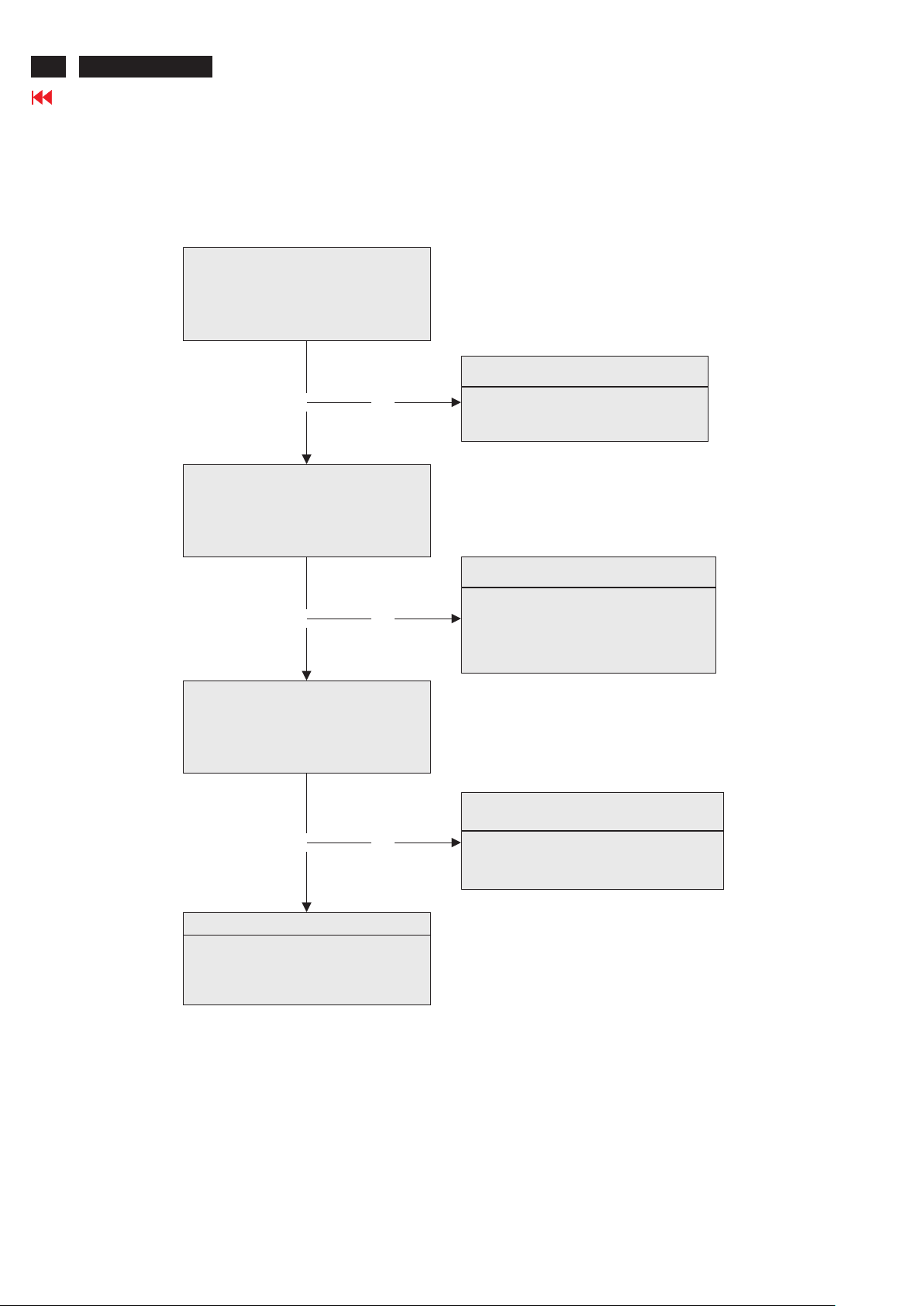
Does OSM display when you
push “MENU key.
Yes No
Proceed "No OSM display"
section.
Check if the sync signal from
computer is output and if the
video cable is connected
normally.
OK
Proceed "checking the resolution
change IC movement" section.
NG
Input the sync signal of computer,
or change the cable.
When a signal isn't being
inputted, it is indicated with "No
Signal Input". it is indicated with
"Out Of Range" at the time of the
frequency that it can't be
distinguished.
5.1 Troublesh ooting for A cer A211H/A221 HQ(1A1D1 H):
5.1.1 No display on the screen (Screen is black and colour of LED is amber):
ACER A211H/A221HQ
Go to contents page
21
Page 24
Is backlight lit?
Refer "Checking the backlight unit" section"OK NG
Does computer output RGB
video signals?
OK
Check OSM menu is display
on screen when you push
the "MENU" key.
Proceed "Abnormal sreen"
dection"
OK
NG
Check the video cable for failure. Check the
host for output signal is all black or not.
1) Change pattern of video signal output on
the host.
2) Reconnect the video cable.
3) Change the video cable.
NG
Check if the LCD video signal cable is
connected between the Interface Board and
LCD module.
OK
Next Page
NG
Failure Point
The LCD video signal cable is
disconnected.
22
ACER A211H/A221HQ
5. Troubleshooting (continued)
Go to contents page
5.1.2 N othing dis plays on the s creen (Scr een is black a nd colour of L ED is blue):
Page 25
5.1.2 N othing dis plays on the s creen (Scr een is black a nd colour of L ED is blue)c ontinued :
Failure Point
1) The LVDS cable broke between
P307 and LCD module.
2) LCD module is failure.
Failure Point
I304 is failure.
Continue
Check the 5V power supply for
P301 pin 4,5,6.
OK
Check the I304 pin2
if voltage is 3.3V
OK
NG
Check if the voltage
between I304 pin2 and
pin3 is above -0.7V
OK
Check the P307 all LVDS signals.
OK
NG
NG
Proceed "Checking the DC/DC
converter circuit" section.
NG
Check the I304 pin2
if voltage is 5V
Failure Point
1) FB301 is open..
OK
Check the I305 pin2
if voltage is 1.2V
OK
NG
Proceed "Checking the DC/DC
converter circuit" section.
Check the input voltage level
whether was changed when
pressed function keys on the P308
pin1
Check if the voltage
on I308 pin 108 that
is from 3.3V to 0V.
OK
NG
OK
NG
Failure Point
Printed wire broke between P310
pin 1 and I308 pin 108.
Failure Point
I308 is failure
Failure Point
1) Printed wire broke between
P307 and I308 LVDS signals.
2) I308 is failure.
5. Troubleshooting (continued)
ACER A211H/A221HQ
Go to contents page
23
Page 26
Is +22V supplied to inverter
PWB? (by the power board)
OK NG
Failure Point
Power board of Inverter part
failure.
Check the BKLT_EN signal of the
DC input P301 pin 2 at TTL high
level.
OK NG
Failure Point
1) printed wire broke between
P301 pin2, R304 and I308
pin101.
2) I308 is failure.
Check the BKLT_ADJ signal of
the input P301 pin3 from I308
pin102 is a PWM signal.
OK NG
Failure Point
Printed wire broke between P301
pin3, R501 and I308 pin102.
Failure Point
1) Back light unit of LCD module
is failure.
2) Inverter Cable disconnect
24
ACER A211H/A221HQ
Go to contents page
5.1.3 C hecking th e back light u nit:
5. Troubleshooting (continued)
Page 27
5.1.4 A bnormal sc reen( for VG A):
Check the R, G, B video signal from
computer input on P302 of D-sub
connector.
OK NG
Failure Point
1) No R, G, B video signals output
from host computer, check computer.
2) Video signal cable disconnection.
Check the R, G, B input video signals
on I308 pin25, 27, 30 respectively that
their level is 0.0 to 0.7Vp-p.
Failure Point
In the case of the Red signal. (A Green
and Blue signal is the same path, too.)
1) Printed wire broke between P302
pin1 and I308 pin30.
2) Video cable is failure.
3) FB315, FB306, C315 is open.
4) R327 is short or open.
NG
OK
Check all LVDS signals being output
to P307 from I308?
Failure Point
Printed wire broke between I308 and
P307.
NGOK
Proceed "Checking the resolution
change IC movement" section.
5. Troubleshooting (continued)
ACER A211H/A221HQ
Go to contents page
25
Page 28

Check the DVI video signal from
computer input on P303 of DVI
connector.
OK
NG
Failure Point
1) No DVI video signals output from host
computer, check computer.
2) DVI Video signal cable disconnection.
Check the DVI input video signals on
I308 pin 12,13,14,15,16,17,18,19
respectively that differential input
voltage is 150 to 1200mV, and input
commond mode voltage is 3.3V.
Failure Point
In the case of the DVI_RX0+/- signal. (A
DVI_RX1+/-, DVI_RX2+/- and
DVI_RXC+/- signal is the same path,
too.)
1)Printed wire broke between P303 pin
17, 18 and I308 pin 12. 13.
2) Video cable is failure.
3) R350, R355 open.
NG
OK
Check all LVDS signals being output
to P307 from I308?
Failure Point
Printed wire broke between I308 and
P303.
NGOK
Proceed "Checking the resolution
change IC movement" section.
26
ACER A211H/A221HQ
5. Troubleshooting (continued)
Go to contents page
5.1.4 A bnormal sc reen (For DV I and the same f or HDMI):
Page 29

5. Troubleshooting (continued)
Check the input TTL level whether is changed
when pressed function keys on the P310 pin 5,
6 (normal is high level, when push button,
generated low level)
OK NG
Failure Point
1) Function key wire disconnection.
2) Function key wire is failure.
3) Function key board is failure.
Check the input TTL level of I308 pin 50, 51
whether is changed when pressed function
keys.
OK NG
Failure Point
1) Printed wire broke among P310
pin5, R503 and I308 pin50
2) Printed wire broke among P310
pin6 ,R504 and I308 pin51
Failure Point
I308 is failure.
5.1.5 A bnormal OS D display ad just probl em:
ACER A211H/A221HQ
Go to contents page
27
Page 30

Confirm the host computer supplies
DDC2B mode.
OK NG
Failure Point
The host machine is not
communicatiog in DDC2B mode.
OK
Check the output signal of serial data /
clock on I308 pin 59, 58.
OK
NG
Failure Point
I308 is failure.
Check the voltage on P302 pin 9 that is
power DC 5 V.
NG
Failure Point
TheVideo cable is failure.
Check the signal on P302 pin12, 15 that
is serial data / clock signal.
OK NG
Failure Point
The Video cable is failure.
Failure Point
1) Printed wire broke among I308 pin 58,
59, R320, R321 and P302 pin 12,15
2) I308 maybe failure.
3) R434 ,R429 is open.
4) D306 or D308 or C320 or C321 is
shorted.
28
ACER A211H/A221HQ
Go to contents page
5.1.6 A bnormal pl ug and play op eration( f or VGA):
5. Troubleshooting (continued)
Page 31

5. Troubleshooting (continued)
Confirm the host computersupplies
DDC2B mode.
OK
NG
Failure Point
The host machine is not
communicatiog in DDC2B mode.
OK
Check the output signal of serial data /
clock on I308 pin 122,121
OK
NG
Failure Point
I308 is failure.
Check the voltage on P303 pin14 that is
power DC 5 V.
OK
NG
Failure Point
The Video cable is failure.
Check the voltage on P303 pin 7, 6 that
is serial data / clock signal.
OK
NG
Failure Point
The Video cable is failure.
Failure Point
1) Printed wire broke between I308 pin122,
121,R344, R345 and P303 pin7,6
2) I308 maybe failure.
3) R410, R414 is open.
4) D320 or D321 or C339 or C342 is
shorted.
Check the voltage on P303 pin 16 that is
4.5V.
NG
Failure Point
Printed wire broke between P303 pin
14 and pin 16.
5.1.6 A bnormal pl ug and play op eration (F or DVI and the s ame for HDMI ):
ACER A211H/A221HQ
Go to contents page
29
Page 32

Check the horizontal sync signal on P302
pin13 TTL level.
OK NG
Failure Point
Video cable is failure.
Check the horizontal sync signal on I308
pin 22 TTL level.
OK NG
Failure Point
1) Printed wire broke between P302
pin13 and I308 pin22.
2) FB304 , R405 is open.
3) D307 ,R319 or C322 is short.
Failure Point
Proceed "Checking the resolution change
IC movement" section.
Check the vertical sync signal on P302
pin14 TTL level.
OK NG
Failure Point
Video cable is failure.
Check the horizontal sync signal on I308
pin21 TTL level.
OK NG
Failure Point
1) Printed wire broke between P302
pin14 and I308 pin21.
2) FB305 or R331 is open.
3) D310,R318 or C313 is short.
Failure Point
Proceed "Checking the resolution change
IC movement" section.
30
ACER A211H/A221HQ
5. Troubleshooting (continued)
Go to contents page
5.1.7 C hecking th e interfac e circuit of s ync signal :
5.1.7 .1 Checkin g the contro l circuit of h orizonta l sync pluse :
5.1.7 .2 Checking the con trol circu it of vertical sync p luse:
Page 33

5.1.8 Checki ng the resol ution change IC mov ement:
Check +3.3V supply on I304 pin2.
OK NG
Proceed " Checking the DC/DC converter circuit"
section.
Check +1.2V supply on I305 pin 2.
OK NG
Proceed " Checking the DC/DC converter circuit"
section.
Check X301 27MHz clock input to I308 pin
127 and 128 at TTL level.
OK NG
Failure Point
1) Printed wire broke between X301 and I308 pin
127, 128.
2) C351, C352 is short or open.
3) X301 failure.
Check I308 pin 125 RSTB signal is high
level at normal operation.
OK
Check I308 pin 115,116,117 SPI signal.
OK NG
Failure Point
1) Printed wire broke between I308 pin 115, 116,
117 and I309 pin 2, 5,6.
2) I309 is failure.
Failure Point
I308 failure.
Failure Point
1) Printer wire broke between I308 pin 125 and
2) C391 is short.
3) I308 is failure.
NG
5. Troubleshooting (continued)
ACER A211H/A221HQ
Go to contents page
31
Page 34

Check the 5V is output from P301 pin
4,5,6.
OK
NG
Failure Point
1) Power wire disconnection.
2) Power board is failure.
Check the 5V is input to I304 pin3.
OK NG
Failure Point
Printed wire broke between P301 pin
4,5,6 and I304 pin3.
Check the 3.3V is output from I304 pin2,4
Failure Point
I304 is failure or C308 short.
OK
NG
Check the 3.3V is input to I305 pin3.
OK
NG
Failure Point
Printed wire broke between I304 pin2.
4 and I305 pin3.
Check the 1.2V is output from I305 pin2,4.
Failure Point
I305 failure or C311 short.
OK NG
Failure Point
Printed wire broke between I304 pin2,4,
I305 pin3
32
ACER A211H/A221HQ
Go to contents page
5.1.9 C hecking th e DC/DC conv erter circ uit:
5. Troubleshooting (continued)
Page 35

5. Troubleshooting (continued)
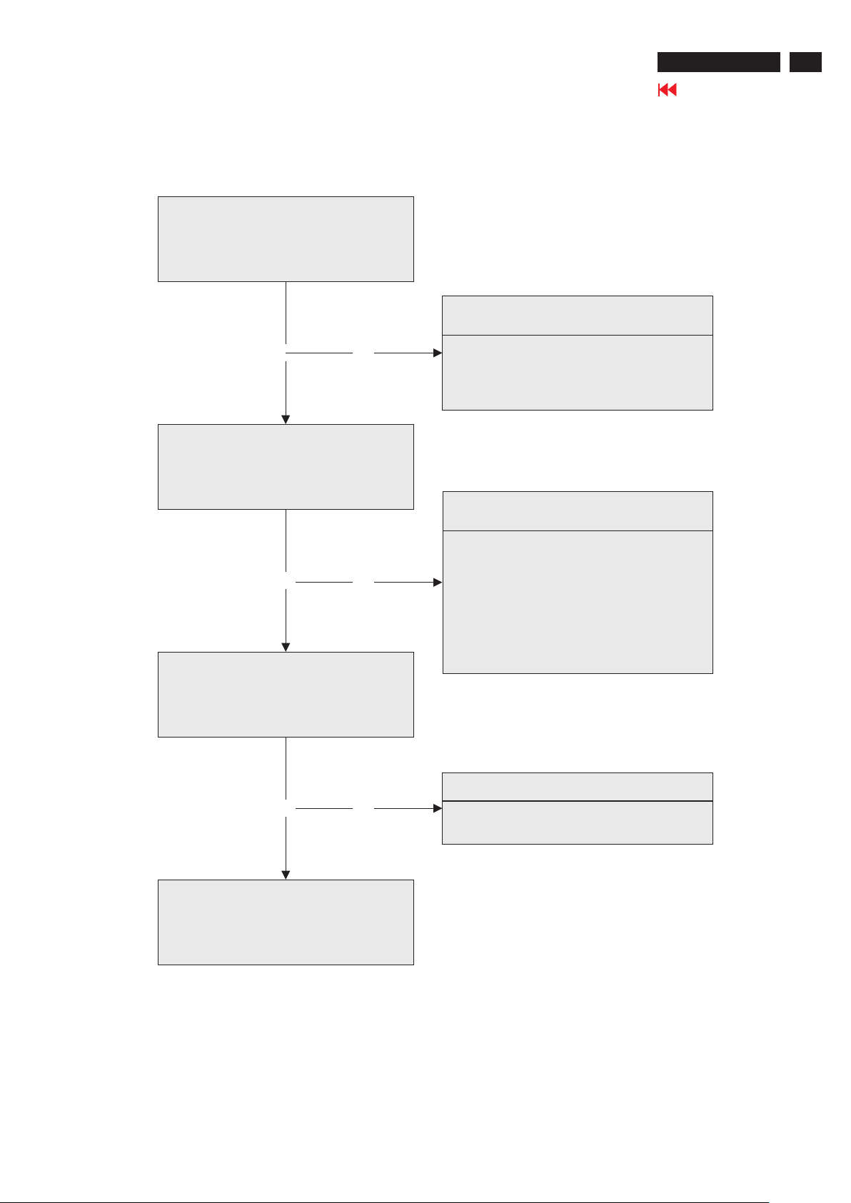
OK
NG Proceed "No OSD display" section.
OK
Proceed "checking the resolution change
IC movement" section.
NG
Input the sync signal of computer, or
change the cable. (VGA or DVI)
When a signal isn't being input, it is
indicated with "VIDEO INPUT". It is
indicated with "OUT OF RANGE" at
the time of the frequency that it can't
be distinguished.
Does OSD display when you push
MENU button.
Check if the sync signal
from computer is output and if the
video cable is connected normally.
(VGA or DVI)
5.2 Troublesh ooting for P 216H/ P226 HQ(1A1D) :
5.2.1 N o display on t he screen (S creen is bla ck and colou r of LED is ambe r):
ACER A211H/A221HQ
Go to contents page
33
Page 36

Refer "Checking the backlight unit" section"
OK
NG
OK
Proceed "Abnormal sreen" section"
OK
NG
Check the video cable for failure. Check the host for output
signal with all black only.
1) Change pattern of video signal output on the host.
2) Reconnect the video cable.
3) Change the video cable. (VGA or DVI)
NG
OK
Next Page
NG
Failure Point
The LVDS cable is disconnected.
Is backlight light up?
Does computer output
RGB video signals? (VGA or DVI)
Check OSD menu is
display on screen when you push
the "MENU" key.
Check if the LCD module
signal cable is connected between
the Interface Board and LCD
module.
34
ACER A211H/A221HQ
5. Troubleshooting (continued)
Go to contents page
5.2.2 N othing dis plays on the s creen (Scr een is black a nd colour of L ED is blue):
Page 37

5. Troubleshooting (continued)
Continue
OK
NG
OK
Failure Point
I301 is failure.
NG
Failure Point
1) Printed wire broke between CN301
pin9, 10, 11 and I301.
2) Check power board.
OK
Failure Point
I302 is failure.
NG
Failure Point
1) Printed wire broke between I301
pin 2, and I302 pin 3.
2) Both D313 and L313 are open.
3) I302 is failure.
NG
Check the 3.3V power are
supplied on I301 pin 2.
Check if the voltage on
I301 pin 3 that is power DC at 5V.
Check the 1.2V power are
supplied on I302.
Check if the voltage
on I302 pin 3 that is power DC at
3.3V from I301.
Next Page
OK
5.2.2 N othing dis plays on the s creen (Scr een is black a nd colour of L ED is blue)c ontinued :
ACER A211H/A221HQ
Go to contents page
35
Page 38

OK
NG
OK
NG
Failure Point
(1) Printed wire broke between
CN301 pin 9, 10,11 and I303 pin 2.
(2) L301 is open.
OK
NG
OK
Failure Point
1) Printed wire broke between Q301
pin 3, R305, R307, C312 and I303
pin G.
2) Q301 is failure.
Failure Point
1) Printed wire broke between Q301
pin 1 and I310 pin 64.
2) R309 is open.
3) I310 is failure.
Failure Point
I303 is failure.
Failure Point
1) Printed wire broke between CN306
and I310 LVDS signals.
2) I310 is failure.
Failure Point
1) The LVDS cable broke between
CN306 and LCD panel module.
2) LCD panel module is failure.
OK
NG
Check the 5V power are
supplied on CN306 pin 1, 2, 3, (to
the LCD panel module)
Check if the Voltage on I303
pin S that is DC power at 5V.
Check if the MOS FET Gate level
on I303 pin G, that Gate level is low.
Check the PANEL
VCC_EN signal of the Q301 pin 1
(with R309) at high level.
NG
Check the CN306 all LVDS signals.
Continue
36
ACER A211H/A221HQ
5. Troubleshooting (continued)
Go to contents page
5.2.2 N othing dis plays on the s creen (Scr een is black a nd colour of L ED is blue)c ontinued :
Page 39

5.2.3 C hecking th e back light u nit:
OK
NG
Failure Point
1) The wire between Power +22V and
Inverter +22V is broken.
2) Power board failure.
OK
NG
Failure Point
1) Printed wire broke between CN301
pin 13, and I310 pin 114.
2) R301 is open.
3) I310 is failure.
Failure Point
Back light unit of LCD module is failure.
Is +22V supplied to inverter PWB?
(by the power board)
Check the BACKLIGHT_ADJ
signal of the CN301 pin 13 from I310
pin 114 is a PWM signal.
5. Troubleshooting (continued)
ACER A211H/A221HQ
Go to contents page
37
Page 40

OK
NG
Failure Point
1) No R, G, B video signals output from
host computer, check computer.
2) VGA video signal cable disconnection.
Failure Point
In the case of the Red signal. (Green and Blue
signal is the same path, too.)
1) Printed wire broke between CN302 pin 1 and
I310 pin 30.
2) Video cable is failure.
3) L303, R313, R314 are open.
4) R315 is short.
5) C316, C318 is short or open.
NG
OK
Failure Point
1) Printed wire broke between I310 and CN306.
2) LVDS wire failure.
NG
OK
Proceed "Checking the resolution change IC
movement" section.
NG
OK
Failure Point
1) Printed wire broke between I306 and P302.
2) L306, R327, R328 are open.
3) R329, R330 if is 2.2K ohm.
4) D305, D306, C330, C331 are short.
5) Video cable is failure.
Check the R, G, B video
signal from computer input on CN302
of video connector.
Check the R, G, B input
video signals on I310 pin 25, 27, 30
respectively that their level is 0.5 to 1.0
Vp-p.
Check the H, V SYNC input signals on
I310 pin 21, 22 respectively that signal
and level.
Check all LVDS signals being output
to CN306 from I310?
38
ACER A211H/A221HQ
Go to contents page
5.2.4 A bnormal sc reen
5.2.4 .1 Abnorma l screen for V GA source
5. Troubleshooting (continued)
Page 41

5. Troubleshooting (continued)
OK
NG
Failure Point
1) No TMDS signals output from host computer,
check computer.
2) DVI-D video signal cable disconnection.
Failure Point
The DVI is high will to generated TMDS from PC
host.
1) Check CN303 pin 14 if is 4.75 to 5V.
2) Printed wire broke between CN303 pin 14
and Pin16.
3) C341 is short, or R342 is open.
5) DVI-D cable is failure.
6) Printed wire broke between CN303 pin 16
and I310 pin 111.
7) I310 is failure.
NG
OK
Failure Point
1) Printed wire broke between I310 and CN306.
2) LVDS cable failure.
NG
OK
Proceed "Checking the resolution change IC
movement" section.
NG
OK
Failure Point
In the case of the RX2+/- signal. (A RX1, 0, and
RXC signal is the same path, too.)
1) Printed wire broke between CN303 pin 1, 2
and I310 pin 16, 17.
2) DVI-D cable is failure.
3) R349, R350 is open.
Check the TMDS signals
from computer input on CN303 of
video connector.
Check the DVI signal to
CN303 pin 16 respectively that voltage
is 4.5 to 5 V.
Check TMDS signals on
I310 pin 12,13,14,15,16,17,18,19
respectively that their differential input
voltage is 150 to 1200 mV.
Check all LVDS signals being output
to CN306 from I310?
5.2.4 .2 Abnorma l screen for D VI source
ACER A211H/A221HQ
Go to contents page
39
Page 42

OK
NG
Failure Point
1) Function key wire disconnection.
2) Function key wire is failure.
3) Function key board is failure.
Check the input level whether was
changed when pressed function keys on the
CN304 pin 1, 2. (Normal is 3.3V, when push button,
genertaed different voltage. Pin 1, 2 is 0.69V or
1.65V or 2.11V)
Check the input level whether was
changed when pressed function keys on the I310 pin
52, 53. (Normal is 3.3V, when push button, genertaed
0.69V or 1.65V or 2.11V)
NG
Failure Point
1) Printed wire broke between CN304 pin 1, I310 pin 52.
2) Printed wire broke between CN304 pin 2, I310 pin 53.
3) C363 or C364 is short.
4) R380 or R381 is short or open.
4) R382 or R383 is open.
Failure Point
I310 is failure
OK
40
ACER A211H/A221HQ
Go to contents page
5.2.5 A bnormal OS D display ad just probl em:
5. Troubleshooting (continued)
Page 43

5.2.6 A bnormal pl ug and play op eration
OK
NG
Failure Point
The host machine is not communicated in DDC/
CI mode.
OK
NG
Failure Point
1) Printed wire broke between I304 pin 8, D307
and CN302 pin 9.
2) D307 is failure.
OK
NG
Failure Point
I304 is failure.
OK
NG
Failure Point
The VGA video cable is failure.
OK
NG
Failure Point
The VGA video cable is failure.
Failure Point
1) Printed wire broke between I310 pin 58, 59,
I304 pin 5, 6 and CN302 pin 12, 15.
2) I310 maybe failure.
3) R334 or R335 is open.
4) C334, C335, R332, R333 is short.
Confirm the host computer supplies
DDC/CI mode.
Check the voltage on CN302 pin 9,
that is DC 5 V.
Check the voltage on I304 pin 8,
that is DC 5 V.
Check the signals if is high
level on CN302 pin 12, 15, that is I2C
data / clk signal.
Check the output signal of I2C
data / clk on I304 pin 5, 6.
5.2.6 .1 Abnorma l plug and pla y operatio n for VGA
5. Troubleshooting (continued)
ACER A211H/A221HQ
Go to contents page
41
Page 44

OK
NG
Failure Point
The host machine is not communicated in DDC/
CI mode.
OK
NG
Failure Point
1) Printed wire broke between I305 pin 8, D311
and CN303 pin 14.
2) D311 is failure.
OK
NG
Failure Point
I305 is failure.
OK
NG
Failure Point
The DVI video cable is failure.
OK
NG
Failure Point
The DVI video cable is failure.
Failure Point
1) Printed wire broke between I310 pin 123,
124, I305 pin 5, 6 and CN303 pin 7, 6.
2) I310 maybe failure.
3) R339 or R340 is open.
4) C338, C339, R337, R338 is short.
Confirm the host computer supplies
DDC/CI mode.
Check the voltage on CN303 pin 14,
that is DC 5 V.
Check the voltage on I305 pin 8,
that is DC 5 V.
Check the signals if is high
level on CN303 pin 7, 6, that is I2C data
/ clk signal.
Check the output signal of I2C
data / clk on I305 pin 5, 6.
42
ACER A211H/A221HQ
Go to contents page
5.1.6 .2 Abnorma l plug and pla y operatio n for DVI
5. Troubleshooting (continued)
Page 45

5. Troubleshooting (continued)
OK
NG
Failure Point
VGA Video cable is failure.
OK
NG
Failure Point
1) Printed wire broke between CN302
pin 13 and I310 pin 22.
2) L306 or R327 is open.
3) R330 or C331 is short.
Failure Point
Process "Checking the resolution change IC
movement" section.
Check the horizontal sync signal
on CN302 pin 13 TTL level.
Check the horizontal sync signal
on I310 pin 22 TTL level.
OK
NG
Failure Point
VGA Video cable is failure.
OK
NG
Failure Point
1) Printed wire broke between CN302
pin 14 and I310 pin 21.
2) R328 is open.
3) R329 or C330 is short.
Failure Point
Process "Checking the resolution change IC
movement" section.
Check the vertical sync signal
on CN302 pin 14 TTL level.
Check the vertical sync signal
on I310 pin 21 TTL level.
5.2.7 C hecking th e interfac e circuit of s ync signal :
5.2.7 .1 Checkin g the contro l circuit of h orizonta l sync pluse :
ACER A211H/A221HQ
Go to contents page
43
5.2.7 .2 Checking the con trol circu it of vertical sync p luse:
Page 46

OK
NG
Proceed " Checking the DC/DC converter
circuit" section.
OK
NG
Proceed " Checking the DC/DC converter
circuit" section.
OK
NG
Failure Point
1) Printed wire broke between X301 and I310
pin 127, 128.
2) C360, C361 is short or open.
3) X301 is failure.
OK
NG
Failure Point
1) Check I310 pin125 is from high to low level, it
is 3~10ms high level, when VCC5V is turned
on.
2) Printed wire broke between I310 pin 125 and
C362/R376.
3) R376 is short or open..
4) I310 failure.
OK
NG
Failure Point
1) Printed wire broke between I310 pin 115~118
and I307.
2) I311 failure.
Failure Point
I310 failure.
Check +3.3V supply on I310 pin 49, 84,
106, 62, 1
Check +1.2V supply on I310 pin 60,
73, 120. 23
Check X301 14.318MHz clock input to
I310 pin 127 and 128
Check I310 pin 125 RESET signal is
high level at normal operation.
Check I310 pin 115~118 SPI Flash
ROM interface signal.
44
ACER A211H/A221HQ
5. Troubleshooting (continued)
Go to contents page
5.2.8 Checki ng the resol ution change IC mov ement:
Page 47

5.2.9 C hecking th e DC/DC conv erter circ uit:
OK
NG
Failure Point
1) Power wire disconnection.
2) Power board is failure.
OK
NG
Failure Point
Printed wire broke between CN301
pin 9, 10, 11 and I301 pin3.
Failure Point
I301 is failure or C304 is short.
OK NG
OK
NG
Failure Point
I302 failure or both C308 and C310
short..
Failure Point
Printed wire broke between I302 pin2 and
L308 L310.
Printed wire broke between I301 pin2 and
L307 L309 L311
L307 L309 L311 L308 L310 open or C345
C346 C347 C350 C351 C352 C356 C357
C348 C349 C382 C353 C354 C355 short.
Check the 5V is output from
CN301 pin 9,10,11
Check the 5V is input to I301 pin3
Check the 3.3V is output
from I301 pin2
Check the 1.2V is output
from I302 pin2
Check the 3.3V or 2.6V is
input to I302 pin3
OK
Failure Point
Printed wire broke between I301 pin2
and I302 pin3. Or both D313 and
L313 open or C307 short.
NG
5. Troubleshooting (continued)
ACER A211H/A221HQ
Go to contents page
45
Page 48

OK
NG Proceed "No OSD display" section.
OK
Proceed "checking the resolution change
IC movement" section.
NG
Input the sync signal of computer, or
change the cable. (VGA)
When a signal isn't being input, it is
indicated with "VIDEO INPUT". it is
indicated with "OUT OF RANGE" at
the time of the frequency that it can't
be distinguished.
Does OSD display when you push
MENU button.
Check if the sync signal
from computer is output and if the
video cable is connected normally.
(VGA)
46
ACER A211H/A221HQ
5. Troubleshooting (continued)
Go to contents page
5.3 Troublesh ooting for A cer A211H/A221 HQ(1A):
5.3.1 N o display on t he screen (S creen is bla ck and colou r of LED is ambe r):
Page 49

5. Troubleshooting (continued)
Refer "Checking the backlight unit" section"
OK
NG
OK
Proceed "Abnormal sreen" dection"
OK
NG
Check the video cable for failure. Check the host for output
signal with all black only.
1) Change pattern of video signal output on the host.
2) Reconnect the video cable.
3) Change the video cable. (VGA)
NG
OK
NG
Failure Point
The LVDS cable is disconnected.
Is backlight light up?
Does computer output
RGB video signals? (VGA)
Check OSD menu is
display on screen when you push
the "MENU" key.
Check if the LCD module
signal cable is connected between
the Interface Board and LCD
module.
OK
NG
OK
Failure Point
I301 is failure.
NG
Failure Point
1) Printed wire broke between CN301
pin9, 10, 11 and I301.
2) Check power board.
OK
Failure Point
1) Printed wire broke between Q302
Pin C and D301 Pin A.
2)D301 or Q302 is failure.
NG
Failure Point
1) Printed wire broke between I301
pin 2, and Q302 pin E.
2) I301 is failure.
NG
Check the 3.3V power are
supplied on I301 pin 2.
Check if the voltage on
I301 pin 3 that is power DC at 5V.
Check the 1.2V power are
supplied on D301.
Check if the voltage
on Q302 pin E that is power DC at
3.3V from I301.
Next Page
OK
5.3.2 N othing dis plays on the s creen (Scr een is black a nd colour of L ED is blue):
ACER A211H/A221HQ
Go to contents page
47
Page 50

OK
NG
OK
NG
Failure Point
Printed wire broke between CN301
pin 9, 10,11 and I301 pin S.
OK
NG
OK
Failure Point
1) Printed wire broke between Q303
pin 3, R305, R307, C309 and I302
pin G.
2) Q303 is failure.
Failure Point
1) Printed wire broke between Q303
pin 1 and I306 pin 29.
2) I306 is failure.
Failure Point
I302 is failure.
Failure Point
1) Printed wire broke between CN304
and I306 LVDS signals.
2) I306 is failure.
Failure Point
1) The LVDS cable broke between
CN304 and LCD panel module.
2) LCD panel module is failure.
OK
NG
Check the 5V power are
supplied on CN304 pin 1, 2, 3, 4, 5
(to the LCD panel module)
Check if the Voltage on I302
pin S that is DC power at 5V.
Check if the MOS FET Gate level
on I302 pin G, that Gate level is low.
Check the PANEL
VCC_EN signal of the Q303 pin 1
(with R309) at high level.
NG
Check the CN304 all LVDS signals.
Continue
48
ACER A211H/A221HQ
5. Troubleshooting (continued)
Go to contents page
5.3.2 N othing dis plays on the s creen (Scr een is black a nd colour of L ED is blue)c ontinued :
Page 51

5.3.3 C heck the bac klight uni t:
OK
NG
Failure Point
1) The wire between Power +22V and
Inverter +22V is broken.
2) Power board failure.
OK
NG
Failure Point
1) Printed wire broke between CN301
pin 13, and I306 pin 56.
2) R301 is open.
3) I306 is failure.
Failure Point
Back light unit of LCD module is failure.
Is +22V supplied to inverter PWB?
(by the power board)
Check the BACKLIGHT_ADJ
signal of the CN301 pin 13 from I306
pin 56 is a PWM signal.
5. Troubleshooting (continued)
ACER A211H/A221HQ
Go to contents page
49
Page 52

OK
NG
Failure Point
1) No R, G, B video signals output from
host computer, check computer.
2) VGA video signal cable disconnection.
Failure Point
In the case of the Red signal. (Green and Blue
signal is the same path, too.)
1) Printed wire broke between CN302 pin 1 and
I306 pin 13.
2) Video cable is failure.
3) R313, L304, R314 are open.
4) R315 is short.
5) C316, C318 is short or open.
NG
OK
Failure Point
1) Printed wire broke between I306 and CN304.
2) LVDS wire failure.
NG
OK
Process "Checking the resolution change IC
movement" section.
NG
OK
Failure Point
1) Printed wire broke between I306 and CN302.
2) L307, R324, R325 are open.
3) R326, R327 if is 2.2K ohm.
4) D306, D307, C324, C325 are short.
5) Video cable is failure.
Check the R, G, B video
signal from computer input on CN302
of video connector.
Check the R, G, B input
video signals on I306 pin 8, 10, 13
respectively that their level is 0.5 to 1.0
Vp-p.
Check the H, V SYNC input signals on
I306 pin 16, 17 respectively that signal
and level.
Check all LVDS signals being output
to CN304 from I306?
50
ACER A211H/A221HQ
Go to contents page
5.3.4 A bnormal sc reen for VGA so urce:
5. Troubleshooting (continued)
Page 53

5. Troubleshooting (continued)
OK
NG
Failure Point
1) Function key wire disconnection.
2) Function key wire is failure.
3) Function key board is failure.
Check the input level whether was
changed when pressed function keys on the
CN305 pin 1, 2. (Normal is 3.3V, when push button,
generted different voltage. Pin 1, 2 is 0.69V or
1.65V or 2.11V)
Check the input level whether was
changed when pressed function keys on the I306 pin
58, 539. (Normal is 3.3V, when push button,
genertaed 0.69V or 1.65V or 2.11V)
NG
Failure Point
1) Printed wire broke between CN305 pin 2, 1306 pin 58.
2) Printed wire broke between CN305 pin 1, 1306 pin 59.
3) C366 or C367 is short.
4) R370 or R371 is short or open.
4) R372 or R373 is open.
Failure Point
I306 is failure
OK
5.3.5 A bnormal OS D display ad just probl em:
ACER A211H/A221HQ
Go to contents page
51
Page 54

OK
NG
Failure Point
The host machine is not communicated in DDC/
CI mode.
OK
NG
Failure Point
1) Printed wire broke between I303 pin 8, D308
and CN302 pin 9.
2) D308 is failure.
OK
NG
Failure Point
I303 is failure.
OK
NG
Failure Point
The VGA video cable is failure.
OK
NG
Failure Point
The VGA video cable is failure.
Failure Point
1) Printed wire broke between I306 pin 18, 19,
I303 pin 5, 6 and CN302 pin 12, 15.
2) I306 maybe failure.
3) R331 or R332 is open.
4) C328, C329, D310, D311 is short.
Confirm the host computer supplies
DDC/CI mode.
Check the voltage on CN302 pin 9,
that is DC 5 V.
Check the voltage on I303 pin 8,
that is DC 5 V.
Check the signals if is high
level on CN302 pin 12, 15, that is I2C
data / clk signal.
Check the output signal of I2C
data / clk on I303 pin 5, 6.
52
ACER A211H/A221HQ
Go to contents page
5.3.6 A bnormal pl ug and play op eration fo r VGA:
5. Troubleshooting (continued)
Page 55

5. Troubleshooting (continued)
OK
NG
Failure Point
VGA Video cable is failure.
OK
NG
Failure Point
1) Printed wire broke between CN302
pin 13 and I306 pin 16.
2) L307 or R324 is open.
3) R327 or C325 is short.
Failure Point
Process "Checking the resolution change IC
movement" section.
Check the horizontal sync signal
on CN302 pin 13 TTL level.
Check the horizontal sync signal
on I306 pin 16 TTL level.
OK
NG
Failure Point
VGA Video cable is failure.
OK
NG
Failure Point
1) Printed wire broke between CN302
pin 14 and I306 pin 17.
2) R325 is open.
3) R326 or C324 is short.
Failure Point
Process "Checking the resolution change IC
movement" section.
Check the vertical sync signal
on CN302 pin 14 TTL level.
Check the vertical sync signal
on I306 pin 17 TTL level.
5.3.7 C hecking th e interfac e circuit of s ync signal :
5.3.7 .1 Checkin g the contro l circuit of h orizonta l sync pluse :
ACER A211H/A221HQ
Go to contents page
53
5.3.7 .2 Checkin g the contro l circuit of v ertical sy nc pulse:
Page 56

OK
NG
Proceed " Checking the DC/DC converter
circuit" section.
OK
NG
Proceed " Checking the DC/DC converter
circuit" section.
OK
NG
Failure Point
1) Printed wire broke between X301 and I306
pin 26, 25.
2) C388, C389 is short or open.
3) X301 is failure.
OK
NG
Failure Point
1) Check I306 pin54 is from high to low level, it
is 3~10ms high level, when VCC5V is turned
on.
2) Printed wire broke between I306 pin 54 and
C383/R337.
3) R337, C383 is short or open..
4) I306 failure.
OK
NG
Failure Point
1) Printed wire broke between I306 pin 21~24
and I304.
2) I304 failure.
Failure Point
I306 failure.
Check +3.3V supply on I306 pin 51,
6
Check +1.2V supply on I306 pin 30,
53, 15.
Check X301 14.318MHz clock input to I306
pin 1 and 2
Check I306 pin 54 RESET signal is
low level at normal operation.
Check I306 pin 21~24 SPI Flash
ROM interface signal.
54
ACER A211H/A221HQ
5. Troubleshooting (continued)
Go to contents page
5.3.8 C hecking th e resoluti on change IC m ovement:
Page 57

5.3.9 C hecking th e DC/DC conv erter circ uit:
OK
NG
Failure Point
1) Power wire disconnection.
2) Power board is failure.
OK
NG
Failure Point
Printed wire broke between CN301
pin 9, 10, 11 and I301 pin3.
Failure Point
I301 is failure or C303 is short.
OK
NG
OK
NG
Failure Point
D301 is failure or Q302 is failure or
C307 is short.
Failure Point
Printed wire broke between D301 and
L310.
Printed wire broke between I301 pin2 and
L308 L309.
L308 L309 L310 open or C304 C338 C387
C380 C332 C333 C334 C330 C331 short.
Check the 5V is output from
CN301 pin 9,10,11
Check the 5V is input to I301 pin3
Check the 3.3V is output
from I301 pin2
Check the 1.2V is input to D301
5. Troubleshooting (continued)
ACER A211H/A221HQ
Go to contents page
55
Page 58

Check output voltage +5V, +22V are right or not
NG
OK
Check power switch is turn on or not
Check power cord (P802), signal cable (P302), P802,
P103, P104 are connected right or not
Check pin 5 of I801 have same pulse or not
Check pin 1 of T802 have same pulse or not
Check peak voltage of R811 triangle pulse is under 0.8
volt or not
Check feedback circuit around I802, I803 and the other
components and repair them
It is not power board problem
Turn switch on
Check F801, D801, P802 and repair
them
Check R807, D804, I801 and repair
them
Check peripheral component of I801
and repair them
Check Q803, R813, R814, D806
R811, R815 and repair them
Check D804, R807 R811and repair
them
Repair them
OK
NG
OK
NG
Connect it right
OK
NG
OK
NG
Check C807 is over 17V or not
OK NG
OK
NG
OK NG
Check D809, C822, C823. C824, D820, C818, T802 have
same short circuit or the output +5V and+22V are over
load
Check C805 is about DC126V-380V or not
OK
NG
56
ACER A211H/A221HQ
Go to contents page
5.4 Power board troubleshooting(1A1D1H/1A1D/1A):
5.4. 1 No Power (1A1D1H/ 1A1D/1A) :
5. Troubleshooting (continued)
Page 59

5.4.2 For Inverter Circuit on Power Board (1A1D1H/1A1D/1A):
Check C102 pin is around 5V. ON/OFF pin of P802 is over
2V. Brightness pin is external 3.3V
OK NG
Check pin 2 of I101 is 5V
It is not inverter problem
Check R105, C102 and repair
them. Check printed wire
Check R125, R126, R106, R107,
D109, D118, C119 I101 and repair
them
Check R115, R110, I101 and repair
them
Repair I101
Check R137, R118, R119, R117,
R138, and repair them
Repair them
OK NG
OK NG
Check CCFL and repair them. Lock
P103, P104 tightly
OK
NG
NG
Check P11 of I101 is over 2.83V
OK
NG
OK
NGOK
Check P103, P104 are connected right
OK
NG
OK
Check pin 1&pin 16 of I101 is triangle pulse
Check pin 14 of I101, there is soft start edge up to about
1.2V
Check pin 9&pin 10 of I101, there is around 0.91V
from output detection
Check SW MOS (Q101, Q105) work right
Check transformer (T101) to work it and repair it
5. Troubleshooting (continued)
ACER A211H/A221HQ
Go to contents page
57
Page 60

DebugTool_V6.7.exe
58
ACER A211H/A221HQ
Go to contents page
6. Firmware Upgrade Process
Notes: (1) If the firmware version is shown as same as the current
F/W version which you got from Wistron engineers, you
must exit the ISP programming process.
(2) The ISP programming is only required when the
firmware version is previous version compared to the
current version.
6.1 Hardware Configuration:
PC/HOSTMONITOR
Connect VGA
cable betwe en
monitor and k it
Connect USB
cable betwe en
PC and kit
If it shows “No USB Device”, there is a problems with
communication. You should confirm your USB
device whether be detected by your PC device
management or reconnect the USB cable.
S3. Select ISP icon.
6.2 Realtek F/W Configuration:
S1. Launch the utility of “ ”.DebugTool_V6.7.exe
S2. Select Select “USB” and “Serial Flash”.
Note: Relative firmware code can be found in the folder of
“software pack\ISP”, it depend on which model you
want to update: “1A1D1H” is used in the monitor which
have VGA, DVI and HDMI ports;
“1A1D” is used in the monitor which have VGA and DVI
ports;
“1A” is used in the monitor which have VGA port only.
Page 61

6. Firmware Upgrade Process (continued)
ACER A211H/A221HQ
Go to contents page
59
S4. Select the right F/W code for the mode you want to
update. Herein we take the model of 1A1D1H and 1A1D
for example, select “Bin” as “File Type” first, then click
[BigBin] to choose “A211H_RH_M001_0428.BIN” in the
folder of “A211H_RH_M001_0428” or
“A221HQ_RH_M001_0428.BIN” in the folder of
“A221HQ_RH_M001_0428”( you can also select hex as
file type).
6.3 How to check firmware version?
S1. Turn off the monitor, press “Power” and “e” button at the
same time for turning on the monitor.
S2. Press “Menu” button again to enter factory mode, and
you will see the firmware version.
Note: Please pay attention: Don’t change any parameter
which is measured by precise machine before shipping out.
PowerMenue
S5. Press button to update the firmware.
see the message of ‘Pass’ shown on the window, it
means ISP upgrading process is completed.
Once you
Page 62

60
ACER A211H/A221HQ
Go to contents page
7. Writing EDID Process
Notice Notes: Please be noted that 'INI.INI' file must be copied into 'C:\WINDOWS' root
directory before running EDID program. Moreover, please be aware of not changing any
parameters in the 'INI.INI' file. Especially, the upload key must keep '0' to disable file
uploading process in field.
7.1 Writing EDID Procedure:
Hardware Configuration:
1. Connect the PRINTER PLUG of DDC FIXTURE with the
printer port of PC. (Refer to figure 1)
2. Plug USB A PLUG of DDC FIXTURE to USB socket of
Desktop PC. (Refer to figure 2)
3. Extend the DVI cable on DVI EXTENDING SOCKET of
DDC FIXTURE. (Refer to figure 3)
4.1 Connect the D-sub plug of Chroma with D-SUB PLUG of
DDC FIXTURE. (Refer to figure 4)
4.2 Take a video cable then connect the D-SUB PLUG and the
D-sub socket of monitor. (Refer to figure 5)
5. Connect the extended DVI cable to DVI socket of monitor.
(Refer to figure 6)
6. Re-confirm all the connectors are connected well.
DVI EXT ENDING
D-SUB P LUG
PRINT ER PLUG
SOCKE T
USB A
SOCKE T
7.2 Writing VGA/DVI Process:
S1. Chose the folder such as “P226HQ-1A1D”, (Note: It
depends on which model you want to write. 1A is used
in the monitor only have VGA port, 1A1D is used in the
monitor both have VGA and DVI ports
“P226HQ-1A1D” for a example,
“AcerDigedid_20100105_SN.exe” of
.) herein we take
select the
“P226HQ-1A1D”
to execute it.
S2. Select Model: Key in password “cedid” then select
model which one you want to write EDID code that it
depends on panel type.
USB A
PLUG
DVI EXT ENDING
SOCKE T
1 2 3
5
64
CAUTION: The timing of Chroma shall be setup at
T254/P41 before data recording. The detail setting
parameter from chroma .Please See below photo :
cedid
Page 63

7. Writing EDID Process (continued)
S3. Choose “WRITE” from menu then select “Scan S/N And
Write EDID And Test DDC”.
S4. Key in PPID number(22 characters) which you can find
printed on the model lable in the input column and
below empty column. Press write button after key in
S/N.
ACER A211H/A221HQ
Go to contents page
S2. Select Model: Key in password “cedid” then select
model which one you want to write EDID code that it
depends on if the model have audio speakers, if it have
audio speakers, select P226HQ, otherwise select
NO226HQ.
61
S5. When EDID was written successfully that will show
below message on the screen.
A221HQ
2010
2010
17
A221HQ
17
7.3 Writing HDMI Process:
S1. Connect a HDMI cable between monitor and DDC
FIXTURE through HDMI transfer DVI connector. Open
the folder: “P226HQ-1H”, select
“Acer_HDMI_20100104.EXE” to execute.
cedid
S3~S5. The process of writing EDID for HDMI is same as the
process of writing EDID for VGA/DVI.
POWER
HDMI
HDMI
HDMI CABLE
HDMI tr ansfer DVI co nnector
DDC MULTI-CABLE
Page 64

8. ACER_LCD_A211H/A221HQ SCHEMATICS AND LAYOUTS:
8.1 ACER_LCD_A211H/A221HQ_SCHEMATICS_POWER BOARD(1A1D1H/1A1D/1A/):
1 2 3 4 5 6 7 8 9 10 11 12 13
ACER A211H/A221HQ
Go to contents page
62
A
B
C
D
E
F
P801P801
+5V
+
+
1000U/16V
1000U/16V
2
C823
C823
D118
D118
1N4148
1N4148
+22V
21
R818
R818
910/2W
910/2W
3
Q806
Q806
3904
3904
1
GNDGND
JUMPER WIRE
JUMPER WIRE
R106
R106
56K
56K
R107
R107
12K/1%
12K/1%
F8025AF802
5A
J001
J001
C118
C118
3P/3KV
3P/3KV
C119
C119
470P
470P
X7R
X7R
R137
R137
100 1%
100 1%
0805
0805
R118
R118
220 1%
220 1%
0805
0805
GND
9
8
7
6
5
4
3
2
1
GND
P802P802
VOL
MUTE
EN
GND
GND
+5V
+5V
NC
EN PWM
1
2
1
2
R138
R138
100 1%
100 1%
0805
0805
R119
R119
133 1%
133 1%
0805
0805
R012
R012
10K
10K
P103
P103
1
1
2P
2P
2
2
P104
P104
1
1
2P
2P
2
2
140ohm 7.5mA
137ohm 8.0mA
C003
C003
470uF/16V
470uF/16V
R013
R013
1K(NC)
1K(NC)
R010
R010
100K
100K
R0071KR007
R006
R006
A
C006
I001
I001
7
INL
C013
C013
22nF
22nF
R003
R003
4.75K
4.75K
C006
10uF
10uF
4
+OUT_L
PVDDL
-OUT_L
PGNDL
PGNDR
-OUT_R
+OUT_R
INR
12
C014
C014
22nF
22nF
R004
R004
4.75K
4.75K
FB002
FB002
PBY201209T-121Y-N
PBY201209T-121Y-N
JUMP WIRE
JUMP WIRE
J002
J002
J003
J003
JUMP WIRE
JUMP WIRE
C004
C004
1uF
1uF
L001
L001
1
PBY201209T-121Y-N
PBY201209T-121Y-N
L002
L002
3
PBY201209T-121Y-N
PBY201209T-121Y-N
2
17
L003
L003
16
PBY201209T-121Y-N
PBY201209T-121Y-N
L004
L004
18
PBY201209T-121Y-N
PBY201209T-121Y-N
R005
R005
10K
10K
R0091KR009
R019
R019
1K
33K
33K
R022
R022
22K
22K
C019
C019
0.1uF
0.1uF
R0081KR008
1K
C018
C018
0.1uF
0.1uF
C016
C016
C011
C011
220pF
220pF
C012
C012
220pF
220pF
1nF
1nF
D002
D002
R018
R018
33K
33K
R021
R021
22K
22K
C015
C015
1nF
1nF
MMSZ5232BS(NC)
MMSZ5232BS(NC)
P001P001
4
L+
3
L-
2
R-
1
R+
P002
P002
PH-JACK-3P-Green
PH-JACK-3P-Green
1
2
3
D001
D001
MMSZ5232BS(NC)
MMSZ5232BS(NC)
7
GND
6
AIN_R
5
AIN_L
4
GND
3
AOUT_R
2
AOUT_L
1
GND
P003
P003
JWT-A2001WV2-07
JWT-A2001WV2-07
B
C
D
E
C002
ZD001
ZD001
6.8B
6.8B
C008
C008
1uF
1uF
C005
10K(NC)
10K(NC)
100K
100K
C017
C017
0.1uF
0.1uF
C005
1uF
1uF
1K
R016
R016
10K
10K
R011
R011
C020
C020
0.1uF
0.1uF
C001
C001
1uF
1uF
6
13
9
5
R0151KR015
11
1K
14
8
C010
C010
1uF
1uF
C009
C009
1uF
1uF
PBY201209T-121Y-N
PBY201209T-121Y-N
C022
C022
470pF
470pF
470pF
470pF
C002
10uF
10uF
VDD
GND
VOLUME
MUTE
NC
EN
VDC
C021
C021
R002
R002
10K
10K
15
PVDDR
PAM8603
PAM8603
SOP-18
VREF
10
FB001
FB001
F
F801
F801
R802
CT
CT
7
7
8
HV
HV
4
VCC
VCC
OUT
OUT
CS
CS
COMPGND
COMPGND
GND-1
ZD101
ZD101
6.8B
6.8B
R102
R102
174K 1%
174K 1%
0805
0805
J005
J005
R802
SCK103
SCK103
0.33U/275V
0.33U/275V
6
5
3
2
C812
C812
0.01U
0.01U
X7R
X7R
R115 10
R115 10
R103 680K 1%
R103 680K 1%
GND
JUMP WIRE
JUMP WIRE
C801
C801
C813
C813
0.1U
0.1U
X7R
X7R
GND-1 GND-1
C811
C811
470P
470P
X7R
X7R
12
C101
C101
+
+
0.1uF
0.1uF
C102
C102
22UF/50V
22UF/50V
GND
R116 510K
R116 510K
0805
0805
1
DRV1
2
VDD
3
SEL
4
RT1
0805
0805
5
RT
6
ENAPWM
7
PID
8
12
TIMER
+
+
C103
C103
2.2UF/50V
2.2UF/50V
J006
J006
JUMP WIRE
JUMP WIRE
R822
R822
330K
330K
0805
0805
R821
R821
330K
330K
0805
0805
R820
R820
330K
330K
0805
0805
12
+
+
C807
C807
22UF/50V
22UF/50V
R101
R101
22
22
T26
T26
0805
0805
I101
I101
OZ9919
OZ9919
1
DRV2
GND
SSTCMP
OLP2
OLP1
VSEN
ISEN2
ISEN1
1 3
ET-20
ET-20
T801
T801
23
J007
J007
JUMP WIRE
JUMP WIRE
ZD801
ZD801
22B
22B
Q101
Q101
2N7002
2N7002
GND
16
15
14
13
12
11
10
9
42
C819
C819
0.1U/275V(NC)
0.1U/275V(NC)
R815
R815
200/0805
200/0805
0.047UF
0.047UF
C106
C106
X7R
X7R
4
KBP306G
KBP306G
D801
D801
22/1206
22/1206
R108
R108
J008
J008
JUMP WIRE
JUMP WIRE
-
-
R814
R814
0805
0805
R110
R110
3
2
2K
2K
10
10
T26
T26
1
+
+
D806
D806
R813
R813
100/0805
100/0805
GND
R114 100K
R114 100K
T26
T26
R117 10KR117 10K
J009
J009
JUMP WIRE
JUMP WIRE
C805
C805
100U/450V
100U/450V
GND-1
21
R807
R807
0
0
1N4148
1N4148
4
R804
R804
39K
39K
1206
1206
+
+
R806
R806
39K
39K
1206
1206
1206
1206
23
Q803
Q803
1
7N65C
7N65C
I802
I802
LTV817
LTV817
R109
R109
Q102
Q102
2K
2K
3904
3904
0805
0805
Q103
Q103
3906
3906
R113
R113
510K
510K
0805
0805
GND
C806
C806
0.01U/1KV
0.01U/1KV
D803
D803
PG108R
PG108R
D804
D804
UF4005G
UF4005G
L803
L803
BEAD/6mm
BEAD/6mm
C810
C810
100P(NC)
100P(NC)
1KV X7R
1KV X7R
R811
R811
0.51/2W
0.51/2W
GND-1
1
23
C828
C828
4.7U/50V
4.7U/50V
R111
R111
22
22
0805
0805
GND
+
+
R112
R112
510K
510K
0805
0805
C107
C107
68P
68P
NC
NC
GND
R826
R826
1K
1K
0805
0805
I803
I803
AP431
AP431
GNDGND
C152
C152
220P(NC)
220P(NC)
X7R
X7R
GND
1
L
3
G
2
N
GND
1
G801G801
1
GND
R104
R104
10K
10K
T26
T26
R105
R105
100K
100K
0805
0805
GND
I801
I801
LD7575B
LD7575B
C803
C803
NC
NC
X7R
X7R
J004
J004
JUMP WIRE
JUMP WIRE
3.15AH250V
3.15AH250V
C820
C820
470P/250V
470P/250V
GND
C825
C825
470P/250V
470P/250V
7
1
R808
R808
100K 1%
100K 1%
0805
0805
GND
D802
D802
P6KE180A
P6KE180A
21
GND-1
R825
R825
1K
1K
0805
0805
+22V
T802
T802
ER28
ER28
3 10
1
4
5
C802
C802
3300P/250V
3300P/250V
C832
C832
3300P/250V
3300P/250V
C827
C827
0.01UF
0.01UF
X7R
X7R
GND
1
S2
2
G2
3
S1
4
G1
12
+
+
C125
C125
330UF/35V
330UF/35V
GND
Q105
Q105
AOP609
AOP609
9
8
7
6
R827
R827
30.1K 1%
30.1K 1%
0805
0805
GND
D2
D2
D1
D1
D809
D809
2 1
SF34G
SF34G
C816
C816
1000P
1000P
500V X7R
500V X7R
D820
D820
SB1060FCT
SB1060FCT
D810
D810
2 1
SB560
SB560
C821
C821
1000P
1000P
100V X7R
100V X7R
R823
R823
270
270
0805
0805
R824
R824
31.6K 1%
31.6K 1%
0805
0805
8
7
6
5
GND
R851
R851
1K 1%
1K 1%
0805
0805
12
+
+
C135
C135
330UF/35V
330UF/35V
12
+
+
C134
C134
330UF/35V
330UF/35V
+
+
C822
C822
1000U/16V
1000U/16V
T102
T102
1
2
3
4
5
6710
EEL19-B
EEL19-B
1N4148
1N4148
D109
D109
GND
+
+
C818
C818
330U/35V
330U/35V
+
+
1000U/16V
1000U/16V
GND GNDGND
21
D811
D811
27B
27B
R828
R828
1K
1K
0805
0805
R817
R817
1K
1K
0805
0805
L802
L802
BEAD/6mmx2
BEAD/6mmx2
C824
C824
C116
C116
18P/3KV
18P/3KV
R125
R125
3M 1/2W
3M 1/2W
R126
R126
3.3K 1%
3.3K 1%
0805
0805
GND GND
G
J013
J010
J010
JUMP WIRE
JUMP WIRE
J017
J017
JUMP WIRE
JUMP WIRE
J011
J011
JUMP WIRE
JUMP WIRE
J018
J018
JUMP WIRE
JUMP WIRE
J012
J012
JUMP WIRE
JUMP WIRE
J019
J019
JUMP WIRE
JUMP WIRE
J013
JUMP WIRE
JUMP WIRE
J021
J021
JUMP WIRE
JUMP WIRE
J014
J014
JUMP WIRE
JUMP WIRE
J015
J015
JUMP WIRE
JUMP WIRE
1 2 3 4 5 6 7 8 9 10 11 12 13
PCB No.
L9382-SF
G
Page 65

ACER A211H/A221HQ
63
8.2 ACER_LCD_A211H/A221HQ_SCHEMATICS_FUNCTION KEY BOARD(1A1D1H/1A1D/1A):
1 2 3 4 5 6 7 8 9 10 11 12 13
P601
P601
7
A
8
JWT-CON6-12-GP
B
C
D
E
F
G
POWER
1
LEDAMBER
2
LEDBLUE
3
GND
4
ADC2
5
ADC1
6
D607
(NC)MMSZ5234BS-7-F-GP-U
(NC)MMSZ5234BS-7-F-GP-U
D603
D603
A K
D605
D605
AK
1 2
C603 (NC)SCD1U25V3ZY-1GPC603 (NC)SCD1U25V3ZY-1GP
D606
D606
AK
1 2
C604 (NC)SCD1U25V3ZY-1GPC604 (NC)SCD1U25V3ZY-1GP
D607
D604
D604
A K
(NC)MMSZ5234BS-7-F-GP-U
(NC)MMSZ5234BS-7-F-GP-U
(NC)MMSZ5234BS-7-F-GP-U
(NC)MMSZ5234BS-7-F-GP-U
(NC)MMSZ5234BS-7-F-GP-U
(NC)MMSZ5234BS-7-F-GP-U
(NC)MMSZ5234BS-7-F-GP-U
(NC)MMSZ5234BS-7-F-GP-U
12
A K
R606
R606
100R2J-2-GP
100R2J-2-GP
1 2
R607
R607
100R2J-2-GP
100R2J-2-GP
1 2
R601
R601
1 2
100KR3F-GP
100KR3F-GP
R602
R602
1 2
56KR3F-GP
56KR3F-GP
R603
R603
1 2
15KR3F-GP
15KR3F-GP
R604
R604
1 2
100KR3F-GP
100KR3F-GP
R605
R605
1 2
56KR3F-GP
56KR3F-GP
C607
C607
(NC)SCD1U25V3ZY-1GP
(NC)SCD1U25V3ZY-1GP
R608
R608
100R2J-2-GP
100R2J-2-GP
1 2
R609
R609
100R2J-2-GP
100R2J-2-GP
1 2
S601
S601
(NC)SW-TACT-2P-2-GP
(NC)SW-TACT-2P-2-GP
1 2
NP1 NP2
S607
S607
123
4
SW-TACT-173-GP
SW-TACT-173-GP
12
C602
C602
SCD1U25V3ZY-1GP
SCD1U25V3ZY-1GP
12
C606
C606
SCD1U25V3ZY-1GP
SCD1U25V3ZY-1GP
S602
S602
123
SW-TACT-173-GP
SW-TACT-173-GP
S603
S603
123
SW-TACT-173-GP
SW-TACT-173-GP
S604
S604
123
SW-TACT-173-GP
SW-TACT-173-GP
S605
S605
123
SW-TACT-173-GP
SW-TACT-173-GP
S606
S606
123
SW-TACT-173-GP
SW-TACT-173-GP
4
4
4
4
4
Power
12
C601
C601
SCD1U25V3ZY-1GP
SCD1U25V3ZY-1GP
12
C605
C605
SCD1U25V3ZY-1GP
SCD1U25V3ZY-1GP
2 4
1 3
E
AUTO
Menu
Left
Right
D601
D601
(NC)LED-BY-3-GP
(NC)LED-BY-3-GP
Amber
Amber
1
Blue
Blue
2
D602
D602
(NC)LED-BY-3-GP
(NC)LED-BY-3-GP
Amber
Amber
1
Blue
Blue
2
YELLOW
YELLOW
BLUE
BLUE
3
3
D608
D608
LED-BY-9-GP
LED-BY-9-GP
P601
For ESD
R610
R610
1 2
(NC)100KR3F-GP
R611
R611
1 2
R612
R612
1 2
R613
R613
1 2
R614
R614
1 2
E
S602 S606
(NC)100KR3F-GP
(NC)100KR3F-GP
(NC)100KR3F-GP
(NC)100KR3F-GP
(NC)100KR3F-GP
(NC)100KR3F-GP
(NC)100KR3F-GP
(NC)100KR3F-GP
(NC)100KR3F-GP
AUTO
S603 S604 S605
MENU
LEFT < RIGHT >
D602
D601
LED
LED
POWER
Go to contents page
A
B
C
D
E
F
S601
G
1 2 3 4 5 6 7 8 9 10 11 12 13
PCB No.
L0202-1
Page 66

8.3 :
ACER_LCD_A211H/A221HQ_SCHEMATICS_INTERFACE BOARD
8.3.1 ACER_LCD_A211H/A221HQ_SCHEMATICS_INTERFACE BOARD_1A1D1H
8.3.1.1 ACER_LCD_A211H/A221HQ(1A1D1H)_SCHEMATICS_BLOCK DIAGRAM:
1 2 3 4 5 6 7 8 9 10 11 12 13
ACER A211H/A221HQ
Go to contents page
64
A
B
C
D
Power
Board
Brightness, Inv_On/Off
+5V
P301
DC-DC
I304
5v-3.3v
I305
3.3v-1.8v
I307
TMDS
RX0~2+/-,
RXC+/-
DDC
24LC12B
LCD Panel Modul
LVDS
Scaler
RTD2482D-GR V.E.
e
P307
I308
I309
Flash
PM25LV020
X301
XTAL
27MHZ
TQ2 Controll
Board
P306
BLOCK Diagram
er
Upstream
OSD
Key
Board
A
B
C
USB
D
E
F
G
I303
DDC
24LC02B
DDC_SCL_D1
DDC_SDA_D1
DVI-D
Di
gi
Vi
deo
Input
tal
TMDS
RX0~2+/-,
RXC+/-
R,G,B,Hs,Vs
P303
DSUB
Analog
Video
Input
I302
DDC
24LC02B
D_SUB_SCL
D_SUB_SDA
P302
P308
AUDIO PORT
Power
Key
Board
USB
Board
AC
110/220v
Input
AUDIO PORT
Audi o Input
(Reserved)
I306
DDC
24LC02B
DDC_SCL_D1
DDC_SDA_D1
HDMI
HDMI
Input
P305
1 2 3 4 5 6 7 8 9 10 11 12 13
E
F
G
Page 67

ACER A211H/A221HQ
65
8.3.1.2 ACER_LCD_A211H/A221HQ _SCHEMATICS_INTERFACE_BD_POWER:
(1A1D1H)
1 2 3 4 5 6 7 8 9 10 11 12 13
+5V
R477
R477
NC/4K7_5%
NC/4K7_5%
R0402
R0402
A
B
C
P301
P301
STANDBY
BKLT_EN
BKLT_ADJ
+5V
+5V
+5V
GND
GND
MUTE
VOLUME
AUDIO_EN
GND
JWT-A2001WV2-12
JWT-A2001WV2-12
CN20-12
CN20-12
BACKLIGHT_ADJ
1
2
3
4
5
6
7
8
9
10
11
12
NC/0.1uF_16V
NC/0.1uF_16V
CM0402
CM0402
C385
C385
for USB model add R478
R478 NC/0K_5%
MUTE
VOLUME
AUDIO_EN
R302 4K7_5%
R302 4K7_5%
R0402
R0402
R478 NC/0K_5%
0.1uF_16V
0.1uF_16V
CM0402
CM0402
BACKLIGHT_EN
BACKLIGHT_ADJ
C304
C304
P5V
1 3
R0402
R0402
Volume
R301
R301
NC/4K7_5%
NC/4K7_5%
R0402
R0402
Q315
Q315
2
NC/MMBT3904
NC/MMBT3904
SM-NPN
SM-NPN
USB_EN
+5V
FB302 PBY201209T-170Y-S
FB302 PBY201209T-170Y-S
D347 NC/DFLS240L
D347 NC/DFLS240L
R497 0_5%
R497 0_5%
R0402
R0402
USB_EN
BEAD0805
BEAD0805
Power-DI123
Power-DI123
Adj_BACKLIGHT
C301
C301
0.1uF_16V
0.1uF_16V
CM0402
CM0402
P5V
+
+
P5V
C302
C302
100uF_16V
100uF_16V
EC25-63
EC25-63
P5V P3P3V
AP1084K33L
AP1084K33L
TO-263-GOI
TO-263-GOI
C397
C397
0.1uF_16V
0.1uF_16V
CM0402
CM0402
TO263
I304
I304
3
VIN
FB318 NC/PBY201209T-170Y-S
FB318 NC/PBY201209T-170Y-S
D346 S1A
D346 S1A
I305
I305
VI3VO
AP1122DG
AP1122DG
TO-252-GOI
TO-252-GOI
VOUT
TAB
VSS
1
SMA
SMA
TO252
GND14
4
2
4
BEAD0805
BEAD0805
2
+
+
C306
C306
100uF_16V
100uF_16V
EC25-63
EC25-63
C308
C308
0.1uF_16V
0.1uF_16V
CM0402
CM0402
+
+
C310
C310
100uF_16V
100uF_16V
EC25-63
EC25-63
P1P2V
C311
C311
0.1uF_16V
0.1uF_16V
CM0402
CM0402
P1P2V
Go to contents page
P3P3VP5V
A
B
C
D
E
F
G
+5V
MUTE
C386
C386
0.1uF_16V
0.1uF_16V
CM0402
CM0402
AUDIO_EN
C387
C387
0.1uF_16V
0.1uF_16V
CM0402
CM0402
BACKLIGHT_EN
C303
C303
0.1uF_16V
0.1uF_16V
CM0402
CM0402
FB301 PBY201209T-170Y-S
FB301 PBY201209T-170Y-S
BEAD0805
BEAD0805
R404
R404
10K_5%
10K_5%
R0402
R0402
R402
R402
0_5%
0_5%
R0402
R0402
R403
R403
0_5%
0_5%
R0402
R0402
R304
R304
4K7_5%
4K7_5%
R0402
R0402
Audio_MUTE
AUDIO_EN_MCU
on_BACKLIGHT
C312
C312
NC/0.1uF_16V
NC/0.1uF_16V
CM0402
CM0402
I301
I301
AO3419
AO3419
SM-FET
SM-FET
2 3
D
Hole1
Hole1
Case_GND
Case_GND
MH38R75
MH38R75
Hole2
Hole2
Case_GND
Case_GND
MH38R75
MH38R75
E
8
7
6
5
1
2
4
3
8
7
6
5
1
2
4
3
F
VLCD
FB314 PBY201209T-170Y-S
FB314 PBY201209T-170Y-S
1
C376
C376
0.1uF_16V
0.1uF_16V
CM0402
CM0402
BEAD0805
BEAD0805
C377
C377
0.1uF_16V
0.1uF_16V
CM0402
CM0402
VLCD
G
on_Panel
1 2 3 4 5 6 7 8 9 10 11 12 13
PCB No.
L9141-1
Page 68

8.3.1.3 ACER_LCD_A211H/A221HQ(1A1D1H)_SCHEMATICS_INTERFACE_BD_VGA & DDC INTERFACE:
1 2 3 4 5 6 7 8 9 10 11 12 13
ACER A211H/A221HQ
Go to contents page
66
A
B
C
P302
P302
D-SUB_15P
D-SUB_15P
DSUB-15PC
DSUB-15PC
16 17
VGA_5V
VGA_RED
1
9
2
10
3
11
4
12
5
13
6
14
7
15
8
VGA_RED
VGA_5V
VGA_GREEN
VGA_BLUE
VGA_SDA
VGA_CONn
VGA_HSYNC
VGA_REDVGA_VSYNC
VGA_GRNVGA_SCL
VGA_BLU-
D309
D309
NC/MMSZ5232BS
NC/MMSZ5232BS
SOD323
SOD323
D303
D315
D315
MMBD7000
MMBD7000
SOT-23
SOT-23
P5V P5V P5V
1
C325
C325
0.1uF_16V
0.1uF_16V
CM0402
CM0402
VGA_CONn
D303
3
MMBD7000
MMBD7000
SOT-23
SOT-23
2
0.1uF_16V
0.1uF_16V
CM0402
CM0402
R316 100_1%
R316 100_1%
1
C326
C326
R0402
R0402
3
2
D304
D304
MMBD7000
MMBD7000
SOT-23
SOT-23
1
C327
C327
0.1uF_16V
0.1uF_16V
CM0402
CM0402
3
2
D305
D305
MMSZ5232BS
MMSZ5232BS
SOD323
SOD323
VGA_RED-
VGA_GREEN
VGA_GRN-
VGA_BLUE
VGA_BLU-
C323
C323
NC/0.1uF_16V
NC/0.1uF_16V
CM0402
CM0402
FB315
FB315
SBK160808T-110Y-S
SBK160808T-110Y-S
BEAD0603
BEAD0603
FB316
FB316
SBK160808T-110Y-S
SBK160808T-110Y-S
BEAD0603
BEAD0603
FB317
FB317
SBK160808T-110Y-S
SBK160808T-110Y-S
BEAD0603
BEAD0603
C335
C335
NC
NC
CM0402
CM0402
C336
C336
NC
NC
CM0402
CM0402
C334
C334
NC
NC
CM0402
CM0402
FB306
FB306
R326
R326
75_1%
75_1%
R0402
R0402
R323
R323
75_1%
75_1%
R0402
R0402
R324
R324
75_1%
75_1%
R0402
R0402
SBK160808T-600Y-S
SBK160808T-600Y-S
BEAD0603
BEAD0603
FB307
FB307
SBK160808T-600Y-S
SBK160808T-600Y-S
FB308
FB308
SBK160808T-600Y-S
SBK160808T-600Y-S
BEAD0603
BEAD0603
BEAD0603
BEAD0603
C329
C329
5pF
5pF
CM0402
CM0402
C330
C330
5pF
5pF
CM0402
CM0402
C331
C331
5pF
5pF
CM0402
CM0402
R327 75_1%
R327 75_1%
R406 100_1%
R406 100_1%
R322 75_1%
R322 75_1%
R330 100_1%
R330 100_1%
R328 470_1%
R328 470_1%
R325 75_1%
R325 75_1%
R407 100_1%
R407 100_1%
R0402
R0402
R0402
R0402
R0402
R0402
R0402
R0402
R0402
R0402
R0402
R0402
R0402
R0402
C315 47nF_16V
C315 47nF_16V
C317 47nF_16V
C317 47nF_16V
C316 47nF_16V
C316 47nF_16V
C319 47nF_16V
C319 47nF_16V
C328 47nF_16V
C328 47nF_16V
C318 47nF_16V
C318 47nF_16V
C314 47nF_16V
C314 47nF_16V
CM0402
CM0402
CM0402
CM0402
CM0402
CM0402
CM0402
CM0402
CM0402
CM0402
CM0402
CM0402
CM0402
CM0402
VGA_DETn
VGA_DETn
RTD_R+
RTD_R-
RTD_G+
RTD_G-
RTD_B+
RTD_B-
SOG
R476
R476
NC/1M_5%
NC/1M_5%
R0402
R0402
A
B
C
D
E
F
G
FB304 SBK160808T-451Y-S
FB304 SBK160808T-451Y-S
FB305 SBK160808T-451Y-S
FB305 SBK160808T-451Y-S
P5V
VGA_5V
C388
C388
0.1uF_16V
0.1uF_16V
CM0402
CM0402
VGA_SCL
VGA_SDA DDC_SDA_VGA
R320
R321
R321
47_1%
47_1%
R0402R320
R0402
47_1%
47_1%
R0402
R0402
BEAD0603
BEAD0603
BEAD0603
BEAD0603
D311
D311
BAT54C
BAT54C
SOT-23-BAT54
SOT-23-BAT54
D308
D308
MMSZ5232BS
MMSZ5232BS
SOD323
SOD323
D348
D348
MMSZ5232BS
MMSZ5232BS
SOD323
SOD323
D306
D306
MMSZ5232BS
MMSZ5232BS
SOD323
SOD323
D310
D310
MMSZ5232BS
MMSZ5232BS
SOD323
SOD323
R314
R314
4K7_5%
4K7_5%
R0402
R0402
C320
C320
47pF_25V
47pF_25V
CM0402
CM0402
R318
R318
2K4_5%
2K4_5%
R0402
R0402
R315
R315
4K7_5%
4K7_5%
R0402
R0402
C321
C321
47pF_25V
47pF_25V
CM0402
CM0402
D307
D307
MMSZ5232BS
MMSZ5232BS
SOD323
SOD323
R319
R319
2K4_5%
2K4_5%
R0402
R0402
C324
C324
0.1uF_16V
0.1uF_16V
CM0402
CM0402
DDC_SCL_VGA
R405 100_1%
R405 100_1%
R331 100_1%
R331 100_1%
R0402
R0402
R0402
R0402
DDC5V_VGA
I302
I302
8
VCC
7
WP
6
SCL
5
SDA
M24C02_WMN6T
M24C02_WMN6T
SOIC-8P
SOIC-8P
GND
RTD_H
C313
C313
22pF_50V
22pF_50V
CM0402
CM0402
C322
C322
12pF_25V
12pF_25V
CM0402
CM0402
RTD_V
D
E
R408
R408
10K_5%
10K_5%
R0402
R0402
1
A0
2
A1
3
A2
4
R317 100_1%
R317 100_1%
R0402
R0402
DDC_WP
DDC_SCL_VGADDC_SCL_VGA
DDC_SDA_VGADDC_SDA_VGA
DDC_SCL_VGA
DDC_SDA_VGA
F
G
1 2 3 4 5 6 7 8 9 10 11 12 13
PCB No.
L9141-1
Page 69

8.3.1.4 ACER_LCD_A211H/A221HQ _SCHEMATICS_INTERFACE_BD_DVI&DDC INTERFACE:
(1A1D1H)
1 2 3 4 5 6 7 8 9 10 11 12 13
ACER A211H/A221HQ
Go to contents page
67
A
B
C
P303
P303
27
RX2-
29
RX2+
31
GND
RX4-
RX4+
SCL
SDA
VS
RX1-
RX1+
GND
RX3-
RX3+
5V
GND
HP
RX0-
RX0+
GND
RX5-
RX5+
GND
RXC+
RXC-
32
30
28
DVI-D_24P
DVI-D_24P
DVI-24PA
DVI-24PA
DVI_RX2DVI_RX2+
DVI_RX1-
1
2
3
4
5
6
7
8
9
10
11
12
13
14
15
16
17
18
19
20
21
22
23
24
DVI_RX2DVI_RX2+
DVI_SCL
DVI_SDA
DVI_RX1DVI_RX1+
DVI_5V
DVI_CONn
DVI_5V
D323
D323
NC/MMSZ5232BS
NC/MMSZ5232BS
SOD323
SOD323
DVI_5V
DVI_5V
C338
C338
0.1uF_16V
0.1uF_16V
CM0402
CM0402
R340
R340
1K_5%
1K_5%
R0402
R0402
D324
D324
MMSZ5232BS
MMSZ5232BS
SOD323
SOD323
C337
C337
0.1uF_16V
0.1uF_16V
CM0402
CM0402
DVI_CONn
R341 100_1%
R341 100_1%
R505 100_1%
R505 100_1%
R0402
R0402
R0402
R0402
DVI_RX1+
DVI_RX0-DVI_RX0DVI_RX0+DVI_RX0+
DVI_RXC+DVI_RXC+
DVI_RXC-DVI_RXC-
R343 10_5% R0402R343 10_5% R0402
R347 10_5% R0402R347 10_5% R0402
R349 10_5% R0402R349 10_5% R0402
R346 10_5% R0402R346 10_5% R0402
C340
D322
D322
MMSZ5232BS
MMSZ5232BS
SOD323
SOD323
R355 10_5% R0402R355 10_5% R0402
R350 10_5% R0402R350 10_5% R0402
R336 10_5% R0402R336 10_5% R0402
R348 10_5% R0402R348 10_5% R0402
C340
0.1uF_16V
0.1uF_16V
CM0402
CM0402
HDCP_HPDn
DVI_RXC-DVI_RX1+
DVI_DETn
HDCP_HPDn
RX2N
RX2P
RX1N
RX1P
DVI_DETn
RX0N
RX0P
RXCP
RXCN
A
B
C
D
E
F
G
DVI_SCL
DVI_SDA
P5V
DVI_5V
R345
R344
R344
D325
D325
BAT54C
BAT54C
SOT-23-BAT54
SOT-23-BAT54
47_1%
47_1%
R0402R345
R0402
47_1%
47_1%
R0402
R0402
MMSZ5232BS
MMSZ5232BS
SOD323
SOD323
D321
D321
MMSZ5232BS
MMSZ5232BS
SOD323
SOD323
D349
D349
D320
D320
MMSZ5232BS
MMSZ5232BS
SOD323
SOD323
R338
R338
12K_5%
12K_5%
R0402
R0402
C342
C342
47pF_25V
47pF_25V
CM0402
CM0402
R339
R339
12K_5%
12K_5%
R0402
R0402
C339
C339
47pF_25V
47pF_25V
CM0402
CM0402
C341
C341
0.1uF_16V
0.1uF_16V
CM0402
CM0402
DDC_SCL_DVI
DDC_SDA_DVI
DDC5V_DVI
I303
I303
8
VCC
7
WP
6
SCL
5
SDA
M24C02_WMN6T
M24C02_WMN6T
SOIC-8P
SOIC-8P
GND
R460
R460
NC/10K_5%
NC/10K_5%
R0402
R0402
D341
R462
R462
NC/10K_5%
NC/10K_5%
R0402
R0402
R337
R337
10K_5%
10K_5%
R0402
R0402
1
A0
2
A1
3
A2
4
D341
1
I/O 1
GND
I/O 23I/O 3
IP4223-CZ6
IP4223-CZ6
SOT23-6
SOT23-6
R0402
R0402
I/O 4
VCC
2
R464
R464
NC/10K_5%
NC/10K_5%
R0402
R0402
R342 100_1%
R342 100_1%
6
5
4
DDC_SCL_DVIDDC_SCL_DVI
DDC_SDA_DVIDDC_SDA_DVI
P5V P5V
C378
C378
0.1uF_16V
0.1uF_16V
CM0402
CM0402
R465
R465
NC/10K_5%
NC/10K_5%
R0402
R0402
DDC_WP
DDC_SCL_DVI
DDC_SDA_DVI
DVI_RX2-DVI_RX0-
R463
R463
NC/10K_5%
NC/10K_5%
R0402
R0402
D342
D342
1
2
IP4223-CZ6
IP4223-CZ6
SOT23-6
SOT23-6
DVI_RX2+DVI_RX0+
R466
R466
NC/10K_5%
NC/10K_5%
R0402
R0402
I/O 1
GND
I/O 23I/O 3
R461
R461
NC/10K_5%
NC/10K_5%
R0402
R0402
I/O 4
VCC
DVI_RXC+DVI_RX1-
D
6
5
4
C379
C379
0.1uF_16V
0.1uF_16V
CM0402
CM0402
E
R467
R467
NC/10K_5%
NC/10K_5%
R0402
R0402
F
G
1 2 3 4 5 6 7 8 9 10 11 12 13
PCB No.
L9141-1
Page 70

8.3.1.5 ACER_LCD_A211H/A221HQ _SCHEMATICS_INTERFACE_BD_HDMI:
(1A1D1H)
1 2 3 4 5 6 7 8 9 10 11 12 13
P305
P305
20
A
B
C
D
SHELL1
21
SHELL2
HDMI_19P
HDMI_19P
HDMI-DIP-19P
HDMI-DIP-19P
D2 Shield
D1 Shield
D0 Shield
CK Shield
CE Remote
DDC CLK
DDC DATA
HP DET
D2+
D2-
D1+
D1-
D0+
D0-
CK+
CK-
NC
GND
+5V
1
2
3
4
5
6
7
8
9
10
11
12
13
14
15
16
17
18
19
C349
C349
0.1uF_16V
0.1uF_16V
CM0402
CM0402
0.1uF_16V
0.1uF_16V
CM0402
CM0402
C390
C390
0.1uF_16V
0.1uF_16V
CM0402
CM0402
P5V
C389
C389
D338
D338
R480 NC/0_5%
R480 NC/0_5%
HDMI_5V
HDMI_5V
DET_HDMI
D339
D339
MMSZ5232BS
MMSZ5232BS
SOD323
SOD323
R0402
R0402
R359
R359
1K_5%
1K_5%
R0402
R0402
D340
D340
MMSZ5232BS
MMSZ5232BS
SOD323
SOD323
DET_HDMI
HDMI_HPD
R484 0_5% R0402R484 0_5% R0402
R485 0_5% R0402R485 0_5% R0402
R486 0_5% R0402R486 0_5% R0402
R487 0_5% R0402R487 0_5% R0402
R488 0_5% R0402R488 0_5% R0402
R489 0_5% R0402R489 0_5% R0402
R490 0_5% R0402R490 0_5% R0402
R491 0_5% R0402R491 0_5% R0402
HDMI_SCL
HDMI_SDA
D327
D327
NC/MMSZ5232BS
NC/MMSZ5232BS
SOD323
SOD323
HDMI1_D2+
HDMI1_D2HDMI1_D1+
HDMI1_D1HDMI1_D0+
HDMI1_D0HDMI1_CK+
HDMI1_CKCEC
R470
R470
10K_5%
10K_5%
R0402
R0402
HDMI1_D0-
R472
R472
10K_5%
10K_5%
R0402
R0402
HDMI1_D2+
HDMI1_D2HDMI1_D1+
HDMI1_D1HDMI1_D0+
HDMI1_D0HDMI1_CK+
HDMI1_CKCEC
D344
D344
1
I/O 1
2
GND
I/O 23I/O 3
IP4223-CZ6
IP4223-CZ6
SOT23-6
SOT23-6
HDMI1_D0+
HDMI1_D1+
R468
R468
10K_5%
10K_5%
R0402
R0402
I/O 4
VCC
HDMI1_D1-
6
5
4
R473
R473
10K_5%
10K_5%
R0402
R0402
P5V
C381
C381
0.1uF_16V
0.1uF_16V
CM0402
CM0402
D354
D354
NC
NC
SOD523
SOD523
D355
D355
NC
NC
SOD523
SOD523
HDMI1_D2-
R471
R471
10K_5%
10K_5%
R0402
R0402
HDMI_SDA
HDMI_SCL
R474
R474
10K_5%
10K_5%
R0402
R0402
D343
D343
1
I/O 1
2
GND
I/O 23I/O 3
IP4223-CZ6
IP4223-CZ6
SOT23-6
SOT23-6
D345
D345
1
I/O 1
2
GND
I/O 23I/O 3
IP4223-CZ6
IP4223-CZ6
SOT23-6
SOT23-6
HDMI1_D2+
I/O 4
VCC
HDMI1_CK-
R469
R469
10K_5%
10K_5%
R0402
R0402
I/O 4
VCC
6
5
4
6
5
4
HDMI1_CK+
C380
C380
0.1uF_16V
0.1uF_16V
CM0402
CM0402
R475
R475
10K_5%
10K_5%
R0402
R0402
DDC5V_HDMI
P5V
C382
C382
0.1uF_16V
0.1uF_16V
CM0402
CM0402
A
B
C
D
ACER A211H/A221HQ
Go to contents page
68
E
F
G
P5V
HDMI_5V
BAT54C
BAT54C
SOT-23-BAT54
SOT-23-BAT54
D351
D351
NC/MMSZ5232BS
NC/MMSZ5232BS
SOD323
SOD323
HDMI1_SDA
HDMI1_SCL
HDMI_SCL
HDMI_SDA
DDC5V_HDMI
D350
D350
MMSZ5232BS
MMSZ5232BS
SOD323
SOD323
R358
R356
R356
C395
C395
NC/47pF_25V
NC/47pF_25V
CM0402
CM0402
100_1%
100_1%
R0402R358
R0402
100_1%
100_1%
R0402
R0402
4K7_5%
4K7_5%
R0402
R0402
R352
R352
R353
R353
C396
C396
NC/47pF_25V
NC/47pF_25V
CM0402
CM0402
4K7_5%
4K7_5%
R0402
R0402
10K_5%
10K_5%
R354
R354
R479
R479
R0402
R0402
DDC5V_HDMI
I306
I306
8
VCC
7
WP
6
SCL
5
SDA
M24C02_WMN6T
M24C02_WMN6T
SOIC-8P
SOIC-8P
100_1%
100_1%
R0402
R0402
A0
A1
A2
VSS
1
2
3
4
DDC_WP
C350
C350
0.1uF_16V
0.1uF_16V
CM0402
CM0402
1 2 3 4 5 6 7 8 9 10 11 12 13
PCB No.
L9141-1
E
F
G
Page 71

8.3.1.6 ACER_LCD_A211H/A221HQ _SCHEMATICS_INTERFACE_BD_SCALER/RTD2482D:
(1A1D1H)
1 2 3 4 5 6 7 8 9 10 11 12 13
ACER A211H/A221HQ
Go to contents page
69
A
B
C
D
E
F
C373
C373
0.1uF_16V
0.1uF_16V
CM0402
CM0402
I307
I307
1
A0
2
A1
3
A2
GND4SDA
M24C16_WMN6T
M24C16_WMN6T
SOIC-8P
SOIC-8P
R438
R438
10K_5%
10K_5%
R0402
R0402
R431
R431
NC/10K_5%
NC/10K_5%
R0402
R0402
VCC
WP
SCL
PVCC_3V3
C372
C372
0.1uF_16V
0.1uF_16V
CM0402
CM0402
8
7
6
5
LED_1
LED_2
KEY2_SCL
KEY1_SDA
PVCC_3V3
I309
I309
8
VDD
7
HOLD#
3
WP#
VSS4SDI
PM25LV010A
PM25LV010A
SOIC-8P
SOIC-8P
R440
R440
4K7_5%
4K7_5%
R0402
R0402
R411 0_5%
R411 0_5%
Volume
2
SDO
1
CE#
6
SCK
5
C400
C400
NC
NC
CM0402
CM0402
WP_PRO
R0402
R0402
R399 0_5% R0402R399 0_5% R0402
R398 0_5% R0402R398 0_5% R0402
LED_1
LED_2
KEY2_SCL
KEY1_SDA
R492 4K7_5%
R492 4K7_5%
R0402
R0402
R423 22_1% R0402R423 22_1% R0402
R428 22_1% R0402R428 22_1% R0402
R432 22_1% R0402R432 22_1% R0402
R391
R391
R427 100_1%
R427 100_1%
P5V
R430
R430
4K7_5%
4K7_5%
R0402
R0402
1 3
Shielding
22_1% R0402
22_1% R0402
R0402
R0402
EESCL
EESDA
Q314
Q314
2
MMBT3904
MMBT3904
SM-NPN
SM-NPN
CEC
HDMI_HPD
HDCP_HPDn
P1P2V
R442 NC/0_5%
R442 NC/0_5%
R0402
R0402
PVCC_3V3
R389
R389
27K_5%
27K_5%
R0402
R0402
SDOUT
CE
CLK
SDIN
WP
P3P3V
P3P3V
FB311 PBY201209T-170Y-S
FB311 PBY201209T-170Y-S
P1P2V
FB312 PBY201209T-170Y-S
FB312 PBY201209T-170Y-S
PVCC_3V3
R459
R459
R0402
R0402
NC/4K7_5%
NC/4K7_5%
Audio_MUTE
AUDIO_EN_MCU
PVCC_3V3
VCCK_1V2
DDC_SCL_DVI
DDC_SDA_DVI
HDMI1_SDA
HDMI1_SCL
PVCC_3V3
PVCC_3V3
R506
R506
NC/4K7_5%
NC/4K7_5%
R0402
R0402
CE
R441
R441
4K7_5%
4K7_5%
R0402
R0402
BEAD0805
BEAD0805
BEAD0805
BEAD0805
R0402
R0402
R363 100_1%
R363 100_1%
PVCC_3V3
POWER
LED_1
/ATTN
LED_2
R483 10K_5%
R483 10K_5%
C371 0.1uF_16V
C371 0.1uF_16V
CM0402
CM0402
R410 22_1% R0402R410 22_1% R0402
R414 22_1% R0402R414 22_1% R0402
R439 22_1% R0402R439 22_1% R0402
R436 22_1% R0402R436 22_1% R0402
R437
R437
4K7_5%
4K7_5%
R0402
R0402
R0402
R0402
C391
C391
NC/1uF_10V
NC/1uF_10V
CM0402
CM0402
PVCC_3V3
FB319 PBY201209T-170Y-S
FB319 PBY201209T-170Y-S
C353
C353
10uF_10V
10uF_10V
CM0805
CM0805
VCCK_1V2
FB320 PBY201209T-170Y-S
FB320 PBY201209T-170Y-S
C357
C357
10uF_10V
10uF_10V
CM0805
CM0805
USB_EN
on_BACKLIGHT
Adj_BACKLIGHT
PVCC_3V3
R0402
R0402
R0402
R0402
R375
R375
R374
R374
NC/4K7_5%
NC/4K7_5%
NC/4K7_5%
NC/4K7_5%
C370
C370
0.1uF_16V
0.1uF_16V
CM0402
CM0402
WP
CLK
SDIN
SDOUT
CE
XO
XI
PVCC_3V3
R426
R426
6K2_5%
6K2_5%
R0402
R0402
TMDS_3V3
BEAD0805
BEAD0805
ADC_1V2
BEAD0805
BEAD0805
R0402
R0402
R501 100_1%
R501 100_1%
102
I308
I308
103
SD2/SPDIF2/TCON[8]/GPIO/IICSCL/PWM1/AR3N
104
SD1/SPDIF1/TCON[5]/GPIO/IRQ/IICSDA/AR2P
105
SD0 / SPDIF0 / TCON[9] / GPIO / AR2N
106
PVCC
107
PGND
108
MCK/TCON[7]/GPIO/AR1P
109
SCK/TCON[3]/GPIO/AR1N
110
WS/TCON[6]/GPIO/SDT
111
SD0/SPDIF0/TCON[4]/GPIO/SPDIF1
112
SD1/ SPDIF1/TCON[9]/GPIO/WS
113
SD2/SPDIF2/TCON[1][11]/GPIO/IrDA/SCK
114
SD3/SPDIF3/TCON[13]/GPIO/VCLK/MCK
115
SPI_SCLK/SeriesData
116
SI/MCU_SCLK
117
SO/SCSB
118
CEB/IRQB
119
GPIO/PWM5/SPDIF1
120
VCCK
121
DDCSCL3/GPIO/AUX-CH_P1
122
DDCSDA3/GPIO/AUX-CH_N1
123
DDCSDA2/GPIO/AUX-CH_N0
124
DDCSCL2/GPIO/AUX-CH_P0
125
RESETB
126
CEC/GPIO/PWM1/SPDIF2
127
XO
128
XI
R433 NC/6K2_5%
R433 NC/6K2_5%
R0402
R0402
TMDS_3V3
101
SD3/ SPDIF3/TCON[10]/GPIO/PWM0/AR3P
DP_VDD/TMDS_VDD
1
2
C354
C354
0.1uF_16V
0.1uF_16V
CM0402
CM0402
LVB3P
LVB3M
LVBCKP
LVBCKM
LVB2P
LVB2M
LVB1P
LVB1M
LVB0P
LVB0M
95
91
97
92
94
98
100
96
99
93
GPIO/PWM5/TCON[0]/AG1N
GPIO/PWM2/TXE0+_10b/AG2P
GPIO/PWM4/TCON[12][3]/AG1P
DHS/TXE0-_8b/TXE2-_10b/ACLKN
DVS/GPIO/PWM1/TXE1-_10b/AG3N
DENA/TXE0+_8b/TXE2+_10b/ACLKP
DCLK/GPIO/PWM0/TXE1+_10b/AG3P
GPIO/PWM3/TCON[11][6]/TXE0-_10b/AG2N
ARED0/ARED2/TXE1-_8b/TXEC-_10b/AB1N
ARED1/ARED3/TXE1+_8b/TXEC+_10b/AB1P
PVCC_3V3
CM0402
CM0402
C362 0.1uF_16V
C362 0.1uF_16V
86
85
88
87
89
90
ARED2/ARED4/TXE2-_8b/TXE3-_10b/AB2N
ARED6/AGRN2/TXE3-_8b/TXO0-_10b/BR1N
ARED4/ARED6/TXEC-_8b/TXE4+_10b/AB3N
ARED3/ARED5/TXE2+_8b/TXE3+_10b/AB2P
ARED5/ARED7/TXEC+_8b/TXE4+_10b/AB3P
79
84
81
83
78
80
82
PVCC
PGND
ARED7/AGRN3/TXE3+_8b/TXO0+_10b/BR1P
AGRN4/GPIO/ABLU2/TXO2-_8b/TXOC-_10b/BG1N
AGRN2/GPIO/AGRN6/TXO1-_8b/TXO2-_10b/BR3N
AGRN0/GPIO/AGRN4/TXO0-_8b/TXO1-_10b/BR2N
AGRN5/GPIO/ABLU3/TXO2+_8b/TXOC+_10b/BG1P
AGRN3/GPIO/AGRN7/TXO1+_8b/TXO2+_10b/BR3P
AGRN1/GPIO/AGRN5/TXO0+_8b/TXO1+_10b/BR2P
RTD2482RD/RTD2482D/RTD2482
QFP128
QFP128
TMDS_REXT
LANE0P/RX2P_0
LANE0N/RX2N_0
LANE1P/RX1P_0
LANE1N/RX1N_0
LANE2P/RX0P_0
LANE2N/RX0N_0
LANE3P/RXCP_0
LANE3N/RXCN_0
DP_GND/TMDS_GND
LANE0P/RX2P_1
LANE0N/RX2N_1
LANE1P/RX1P_1
LANE1N/RX1N_1
LANE2P/RX0P_1
LANE2N/RX0N_1
LANE3P/RXCP_1
LANE3N/RXCN_1
DP_VDD/TMDS_VDD2
3
4
5
HDMI1_D1-
HDMI1_D0-
HDMI1_D0+
6
7
8
HDMI1_D2-
HDMI1_D1+
HDMI1_D2+
9
10
11
HDMI1_CK-
HDMI1_CK+
C383
C383
10uF_10V
10uF_10V
CM0805
CM0805
12
RX0N
13
14
RX0P
RX1N
0.1uF_16V
0.1uF_16V
AVS021AHS022ADC_VDD23B0-24B0+25G0-26G0+27SOG028R0-29R0+30GPI/B1- / V8_7
15
16
17
18
19
20
RX1P
RX2P
RX2N
RXCP
RXCN
RTD_V
RTD_H
C355
C355
CM0402
CM0402
RTD_B-
RTD_B+
C356
C356
0.1uF_16V
0.1uF_16V
CM0402
CM0402
LVA0M
LVA0P
LVA1M
LVA2M
LVA2P
LVACKM
LVACKP
LVA3M
LVA3P
VCCK_1V2
C361
C361
0.1uF_16V
0.1uF_16V
CM0402
CM0402
DET_SOURCE
DET_AUDIO
71
77
75
76
AGRN6/GPIO/ABLU4/TXOC-_8b/TXO3-_10b/BG2N
AGRN7/GPIO/ABLU5/TXOC+_8b/TXO3+_10b/BG2P
RTD_G-
RTD_G+
68
73
70
69
66
72
74
VCCK
ABLU0/ GPIO/ABLU6/TXO3-_8b/TXO4-_10b/BG3N
ABLU1/ GPIO/ABLU7/TXO3+_8b/TXO4+_10b/BG3P
31
SOG
RTD_R-
RTD_R+
65
67
TCON[6][12]/GPIO/PWM3/BCLKN
WS/TCON[7][1]/GPIO/PWM1/BB3P
ABLU7/SCK/TCON[4][2]/GPIO/BB3N
ABLU6/MCK/TCON[5][9]/GPIO/BB2P
SD0/SPDIF0/TCON[0][7]/GPIO/IrDA
ABLU5/SD0/SPDIF0/TCON[13][3]/GPIO/BB2N
TCON[1][8]/PWM2/GPIO
ABLU4/SPDIF1/SD1/TCON[ 7][3]/GPIO/IICSCL/BB1P
ABLU3/SPDIF2/SD2/TCON[ 9][11]/GPIO/IICSDA/BB1N
TCON[3][5]/DDCSDA1/GPIO
TCON[7][10]/DDCSCL1/GPIO
ABLU2/SPDIF3/SD3/TCON[10][8]/GPIO/PWM1/PWM5/BCLKP
TCON[9][11]/B-ADC2/IICSDA/GPIO
TCON[1][4]/B-ADC1/IICSCL/GPIO
TCON[0][5]/BADC0/PWM1/PWM5/GPIO
AUDIO_HOUTR/V8 _0/PWM0/GPIO
AUDIO_HOUTL/V8_1/SD0/GPIO
AUDIO_SOUTR/V8_2/MCK/GPIO
AUDIO_SOUTL/V8_3/SCK/GPIO
SPDIF3/AUDIO_REF/V8_4/WS/GPIO
GPI/B1+ / V8_632ADC_GND
GPI/R1+/V8_1
GPI/R1-/V8_2
GPI/SOG1 / V8_3
GPI/G1+ / V8_4
GPI/G1- / V8_5
37
36
35
34
33
ADC_1V2
C384
C384
10uF_10V
10uF_10V
CM0805
CM0805
A-ADC4/GPIO
A-ADC3/GPIO
A-ADC2/GPIO
A-ADC1/GPIO
A-ADC0/VCLK/GPIO
LS_ADC_VDD
LINE_INR/V8_5/IICSDA/GPIO
LINE_INL/V8_6/IICSCL/GPIO
GPI/V8_0/AHS1
38
DDC_WP
PVCC
PGND
VCCK
V8_7/GPIO
VCLK/AVS1
OSDKEY_EN
64
63
62
61
60
59
58
57
56
55
54
53
52
51
50
49
48
47
46
45
44
43
42
41
40
39
ON
R329 10K_5%
R329 10K_5%
1A1D1H use R493
R493
R493
10K_5%
10K_5%
R0402
R0402
R495
R495
NC/10K_5%
NC/10K_5%
R0402
R0402
1A1H use R495
WP_PRO
C360 0.1uF_16V
C360 0.1uF_16V
C359 0.1uF_16V
C359 0.1uF_16V
R434 22_1% R0402R434 22_1% R0402
R429 22_1% R0402R429 22_1% R0402
EESCL
EESDA
INR
INL
EAR
EAL
R0402
R0402
C367
C367
1uF_10V
1uF_10V
CM0402
CM0402
PVCC_3V3 PVCC_3V3
R494
R494
10K_5%
10K_5%
R0402
R0402
DET_AUDIODET_SOURCE
R496
R496
NC/10K_5%
NC/10K_5%
R0402
R0402
CM0402
ON
KEY2_SCL
KEY1_SDA
CM0402
CM0402
CM0402
C358
C358
10uF_16V
10uF_16V
EC20-5
EC20-5
PVCC_3V3
VCCK_1V2
DDC_SDA_VGA
DDC_SCL_VGA
on_Panel
AUDIO use R494
NON-AUDIO use
R496
C365
C365
0.1uF_16V
0.1uF_16V
CM0402
CM0402
LVB0M
LVB0P
LVB1M
LVB1P
LVB2M
LVB2P
LVBCKM
LVBCKP
LVB3M
LVB3P
LVA0MLVA1P
LVA0P
LVA1M
LVA1P
LVA2M
LVA2P
LVACKM
LVACKP
LVA3M
LVA3P
PVCC_3V3
4K7_5%
4K7_5%
4K7_5%
4K7_5%
R0402
R0402
R0402
R0402
R409
P308
P308
CN20-7
CN20-7
R361
R361
GND
INR
INL
GND
EAR
EAL
R409
R373
R373
PVCC_3V3
7
6
5
4
3
2
1
A2001WV2_07_JWT
A2001WV2_07_JWT
PVCC_3V3
R392
R392
4K7_5%
4K7_5%
R0402
R0402
DET_HDMI
DVI_DETn
VGA_DETn
4K7_5%
4K7_5%
R0402
R0402
R390
R390
4K7_5%
4K7_5%
R0402
R0402
Audi o output
PC-Audi o i nput
LVB0M
LVB0P
LVB1M
LVB1P
LVB2M
LVB2P
LVBCKM
LVBCKP
LVB3M
LVB3P
LVA0M
LVA0P
LVA1M
LVA1P
LVA2M
LVA2P
LVACKM
LVACKP
LVA3M
LVA3P
A
B
C
D
E
F
G
C351 12pF_50V
C351 12pF_50V
CM0402
CM0402
C352 12pF_50V
C352 12pF_50V
CM0402
CM0402
12
X301
X301
27.000MHz
27.000MHz
XTAL-2PB
XTAL-2PB
R435
R435
NC/1M_5%
NC/1M_5%
R0402
R0402
R507 0_5%
R507 0_5%
XI
R0402
R0402
XO
1 2 3 4 5 6 7 8 9 10 11 12 13
PCB No.
L9141-1
G
Page 72

8.3.1.7 ACER_LCD_A211H/A221HQ _SCHEMATICS_INTERFACE_BD_PANEL INTERFACE & KEY
(1A1D1H) :
1 2 3 4 5 6 7 8 9 10 11 12 13
LVB0M
LVB0P
LVB1M
LVB1P
LVB2M
LVB2P
LVBCKM
LVBCKP
LVB3M
LVB3P
LVA0M
LVA0P
LVA1M
LVA1P
LVA2M
LVA2P
LVACKM
LVACKP
LVA3M
LVA3P
P3P3V
KEY2_SCL
KEY1_SDA
R503 NC/100_1%
R503 NC/100_1%
R504 NC/100_1%
R504 NC/100_1%
R0402
R0402
R0402
R0402
A
B
C
LVB0M
LVB0P
LVB1M
LVB1P
LVB2M
LVB2P
LVBCKM
LVBCKP
LVB3M
LVB3P
LVA0M
LVA0P
LVA1M
LVA1P
LVA2M
LVA2P
LVACKM
LVACKP
LVA3M
LVA3P
P3P3V
R0402
R0402
R369
R369
NC/4K7_5%
NC/4K7_5%
R0402
R0402
R371
R371
NC/4K7_5%
NC/4K7_5%
KEY2
KEY1
POWER1
ORANGE_LED1
BLUE_LED2
FOR V273 KEY 6PIN
P310
P310
1
POWER
2
ORANGE
3
BLUE
4
KEY2
5
KEY1
6
GND
NC/A-POINT 6PIN
NC/A-POINT 6PIN
DF100-6P
DF100-6P
VLCD
C375
C375
100uF_16V
100uF_16V
EC25-63
EC25-63
+
+
VLCD
LVB0M
LVB0P
LVB1M
LVB1P
LVB2M
LVB2P
LVBCKM
LVBCKP
LVB3M
LVB3P
LVA0M
LVA0P
LVA1M
LVA1P
LVA2M
LVA2P
LVACKM
LVACKP
LVA3M
LVA3P
R412
R412
100_5%
100_5%
R0402
R0402
P307
P307
32
31
30
29
28
27
26
25
24
23
22
21
20
19
18
17
16
15
14
13
12
11
10
9
8
7
6
5
4
3
2
1
AFN300-N2G11_P-TWO
AFN300-N2G11_P-TWO
FFC-FPC-30P-100
FFC-FPC-30P-100
A
B
C
ACER A211H/A221HQ
Go to contents page
70
D
E
F
G
POWER
P3P3V
P3P3V
R0402
R508 100_1%
R508 100_1%
R0402
FOR H233 POWER KEY 4PIN and X233 KEY 6PIN
R366 4K7_5%
R366 4K7_5%
LED_1
LED_2
R365 10K_5%
R365 10K_5%
R367 4K7_5%
R367 4K7_5%
R364 10K_5%
R364 10K_5%
10K_5%
10K_5%
R0402
R0402
R481
R481
D356
D356
MMSZ5232BS
MMSZ5232BS
SOD323
SOD323
R0402
R0402
R0402
R0402
R0402
R0402
R0402
R0402
ORANGE_LED1
BLUE_LED2
KEY2
KEY1
R370 330_5%
R370 330_5%
Q305
Q305
MMBT3906
MMBT3906
SM-PNP
SM-PNP
R360 330_5%
R360 330_5%
Q308
Q308
MMBT3906
MMBT3906
SM-PNP
SM-PNP
POWER1
R0402
R0402
R0402
R0402
P309
P309
1
POWER
2
ORANGE
3
BLUE
4
GND
5
KEY2
6
KEY1
A2001WV2_06_JWT
A2001WV2_06_JWT
CN20-6
CN20-6
ORANGE_LED1
C368
C368
0.1uF_16V
0.1uF_16V
CM0402
CM0402
BLUE_LED2
C369
C369
0.1uF_16V
0.1uF_16V
CM0402
CM0402
OSDKEY_EN
LED_1
LED_2
KEY2_SCL
KEY1_SDA
/ATTN
/ATTN
KEY2_SCL
KEY1_SDA
LED_1
LED_2
KEY2_SCL
KEY1_SDA
R500 1K_5% R0402R500 1K_5% R0402
R502 0_5% R0402R502 0_5% R0402
R368 100_1%
R368 100_1%
R362 100_1%
R362 100_1%
R0402
R0402
R0402
R0402
C392
C392
0.1uF_16V
0.1uF_16V
CM0402
CM0402
D352
D352
MMSZ5232BS
MMSZ5232BS
SOD323
SOD323
P3P3V
D353
D353
MMSZ5232BS
MMSZ5232BS
SOD323
SOD323
C394
C394
47pF_25V
47pF_25V
CM0402
CM0402
P306
P306
C393
C393
47pF_25V
47pF_25V
CM0402
CM0402
1
2
3
4
5
6
A-POINT 6PIN
A-POINT 6PIN
DF100-6P
DF100-6P
KEY Vin
GND
ATTN
SCL
SDA
GND
FOR H233 OSD KEY 6PIN
D
E
F
G
1 2 3 4 5 6 7 8 9 10 11 12 13
PCB No.
L9141-1
Page 73

LCD Panel
CN301
Power & Inverter
Board
Audio
Input
DVI
Video
Input
CN304
Function Key BD
D-SUBDVI-DCN303
EEPROM
M24C02
EEPROM
M24C02
CN302
DDC_SCL
DDC_SDA
DDC_SCL
DDC_SDA
EEPROM
M24LC16
XTAL
14.318MHz
Regulator
5V-3.3V
5V-1.8V
Scaler
RTD2281
Analog
Video
Input
AC
110/220V
Input
Audio
Optional
PM25LV020
CN306
LVDS
1311
1310
+5V Vcc
1309Dim & Enable
TMDS
8.3.2 ACER_LCD_A211H/A221HQ_SCHEMATICS_INTERFACE BOARD_1A1D:
8.3.2.1 ACER_LCD_A211H/A221HQ(1A1D)_SCHEMATICS_BLOCK DIAGRAM:
1 2 3 4 5 6 7 8 9 10 11 12 13
ACER A211H/A221HQ
Go to contents page
71
A
B
C
D
A
B
C
D
E
F
G
E
F
G
1 2 3 4 5 6 7 8 9 10 11 12 13
Page 74

8.3.2.2 ACER_LCD_A211H/A221HQ(1A1D)_SCHEMATICS_INTERFACE BOARD_POWER:
1 2 3 4 5 6 7 8 9 10 11 12 13
CN301
A
B
C
BKLT_ADJ
BKLT_EN
+5V
+5V
+5V
GND
GND
MUTE
VOLUME
AUDIO_EN
+5V_RTN
STANDBY
GND
BACKLIGHT_ADJ
BACKLIGHT_EN
CN301
13
12
11
10
9
8
7
6
5
4
3
2
1
JWT-CON13-GP
JWT-CON13-GP
BACKLIGHT_ADJ
BACKLIGHT_EN
1 2
R301 100R2J-2-GPR301 100R2J-2-GP
12
C305
C305
(NC)SCD1U16V2ZY-2GP
(NC)SCD1U16V2ZY-2GP
1 2
R302 (NC)100R2J- 2-GPR302 (NC)100R2J- 2-GP
12
C309
C309
(NC)SCD1U16V2ZY-2GP
(NC)SCD1U16V2ZY-2GP
P5V
P5V
MUTE_CTRL
VOLUME_CTRL
AUDIO_EN_CTRL
P5V
12
R361
R361
(NC)100KR2J-1- GP
(NC)100KR2J-1- GP
12
R303
R303
(NC)100KR2J-1- GP
(NC)100KR2J-1- GP
P5V
P5V 3,4,5,6
STANDBY_CTRL 5
BKLT_ADJ 5
BKLT_EN 5
C301
C301
E100U16VM-58-GP
E100U16VM-58-GP
P5V
12
12
LD1117AG-12-AA3-A-R-GP
LD1117AG-12-AA3-A-R-GP
C302
C302
SCD1U16V2ZY-2GP
SCD1U16V2ZY-2GP
I302
I302
3
VIN
2
VOUT
1
GND
I301
I301
UZ1084-G-3D3V-TN3-R-G P
UZ1084-G-3D3V-TN3-R-G P
3
VIN
2
VOUT
1
ADJ/GND
P3P3V
12
C304
C304
E100U16VM-57-GP-U
E100U16VM-57-GP-U
1 2
(NC)PBY201209T-300Y-N-GP
(NC)PBY201209T-300Y-N-GP
K A
S1A-F-GP
S1A-F-GP
12
C307
C307
P1P2V
SCD1U16V2KX-3GP
SCD1U16V2KX-3GP
12
12
C310
C310
C308
C308
SCD1U16V2ZY-2GP
SCD1U16V2ZY-2GP
E100U16VM-57-GP-U
E100U16VM-57-GP-U
L313
L313
D313
D313
P1P2V 5
P3P3V 5,6
A
B
C
ACER A211H/A221HQ
Go to contents page
72
D
E
F
G
4K7R2J-2-GP
4K7R2J-2-GP
MUTE_CTRL
AUDIO_EN_CTRL
VOLUME_CTRL
R304
R304
12
3
Q302
Q302
1
MMBT3904-7-F-GP
MMBT3904-7-F-GP
2
P5V
12
R308
R308
4K7R2J-2-GP
4K7R2J-2-GP
1 2
R310 100R2J-2-GPR310 100R2J-2-GP
1 2
R312 10KR2J-3-GPR312 10KR2J-3-GP
12
C315
C315
SCD1U16V2ZY-2GP
SCD1U16V2ZY-2GP
R360
R360
10KR2J-3-GP
10KR2J-3-GP
1 2
1 2
R306 100R2J-2-GPR306 100R2J-2-GP
P5V
12
R311
R311
4K7R2J-2-GP
4K7R2J-2-GP
MUTE 5
AUDIO_EN 5
VOLUME 5
P5V
PBY201209T-300Y-N-GP
PBY201209T-300Y-N-GP
PANELVCC_EN5
GEN246R158-8-F-A
GEN246R158-8-F-A
M301
M301
2
3
4
5
6
7
L301
L301
1 2
E100U16VM-58-GP
E100U16VM-58-GP
1
8
C311
C311
1 2
12
R390
R390
100KR2J-1-GP
100KR2J-1-GP
12
10KR2J-3-GP
10KR2J-3-GP
R309
R309
4K7R2J-2-GP
4K7R2J-2-GP
R305
R305
1
12
100KR2J-1-GP
100KR2J-1-GP
R307
R307
1 2
3
MMBT3904-7-F-GP
MMBT3904-7-F-GP
2
Q301
Q301
AO3419L-GP
AO3419L-GP
S
12
C312
C312
SCD1U16V2ZY-2GP
SCD1U16V2ZY-2GP
I303
I303
D
VLCD
L302
L302
D
G
1 2
PBY201209T-300Y-N-GP
PBY201209T-300Y-N-GP
12
C313
C313
SCD1U16V2ZY-2GP
SCD1U16V2ZY-2GP
12
C314
C314
SCD1U16V2ZY-2GP
SCD1U16V2ZY-2GP
VLCD 6
E
F
G
1 2 3 4 5 6 7 8 9 10 11 12 13
PCB No.
L9137-1M
Page 75

8.3.2.3 ACER_LCD_A211H/A221HQ(1A1D)_SCHEMATICS_INTERFACE BOARD_VGA&DDC:
1 2 3 4 5 6 7 8 9 10 11 12 13
CN302
CN302
A
B
C
11
VGA_SDA
VGA_HSYNC
VGA_VSYNC
VGA_SCL
VGA_RED VGA_BLUEVGA_GREEN
3
1
2
1 2
C326
C326
SCD1U16V2ZY-2GP
SCD1U16V2ZY-2GP
12
13
14
15
VIDEO-15-130-GP
VIDEO-15-130-GP
D301
D301
MMBD7000-1-GP
MMBD7000-1-GP
1
17
6
1
7
2
8
3
9
4
10
5
16
3
2
1 2
C327
C327
SCD1U16V2ZY-2GP
SCD1U16V2ZY-2GP
VGA_RED-
VGA_RED
VGA_GRN-
VGA_GREEN
VGA_BLU-
VGA_BLUE
VGA_5V
VGA_CONn
D302
D302
MMBD7000-1-GP
MMBD7000-1-GP
D303
D303
3
MMBD7000-1-GP
MMBD7000-1-GP
1
2
1 2
C329
C329
SCD1U16V2ZY-2GP
SCD1U16V2ZY-2GP
P5VP5VP5V
VGA_RED
VGA_RED-
VGA_GREEN
VGA_GRN-
VGA_BLUE
VGA_BLU-
VGA_CONn
R313 0R3J-L-G PR313 0R3J-L-GP
1 2
R318 0R3J-L-G PR318 0R3J-L-GP
1 2
R322 0R3J-L-G PR322 0R3J-L-GP
1 2
12
SBK160808T-750Y-N-GP
SBK160808T-750Y-N-GP
R315
R315
75R2F-2-GP
75R2F-2-GP
12
SBK160808T-750Y-N-GP
SBK160808T-750Y-N-GP
R320
R320
75R2F-2-GP
75R2F-2-GP
12
SBK160808T-750Y-N-GP
SBK160808T-750Y-N-GP
R324
R324
75R2F-2-GP
75R2F-2-GP
D304
D304
MMSZ5234BS-7-F-GP-U
MMSZ5234BS-7-F-GP-U
A K
L303
L303
1 2
L304
L304
1 2
L305
L305
1 2
1 2
R326 1KR2J-1-GPR326 1KR2J-1 -GP
12
C317
C317
(NC)SC5P50V2CN- 2GP
(NC)SC5P50V2CN- 2GP
12
C321
C321
(NC)SC5P50V2CN- 2GP
(NC)SC5P50V2CN- 2GP
12
C324
C324
(NC)SC5P50V2CN- 2GP
(NC)SC5P50V2CN- 2GP
C328
SCD1U16V2ZY-2GP
SCD1U16V2ZY-2GP
C328
R314
R314
1 2
100R2F-L1-GP-U
100R2F-L1-GP-U
R316
R316
1 2
100R2F-L1-GP-U
100R2F-L1-GP-U
R317
R317
(NC)470R2J- 2-GP
(NC)470R2J- 2-GP
1 2
R319
R319
1 2
100R2F-L1-GP-U
100R2F-L1-GP-U
R321
R321
1 2
100R2F-L1-GP-U
100R2F-L1-GP-U
R323
R323
1 2
100R2F-L1-GP-U
100R2F-L1-GP-U
R325
R325
1 2
100R2F-L1-GP-U
100R2F-L1-GP-U
12
C316
1 2
1 2
1 2
1 2
1 2
1 2
1 2
C316
SCD047U16V2KX-1-GP
SCD047U16V2KX-1-GP
C318
C318
SCD047U16V2KX-1-GP
SCD047U16V2KX-1-GP
C319
C319
(NC)SCD047U16V2KX-1-GP
(NC)SCD047U16V2KX-1-GP
SCD047U16V2KX-1-GP
SCD047U16V2KX-1-GP
SCD047U16V2KX-1-GP
SCD047U16V2KX-1-GP
SCD047U16V2KX-1-GP
SCD047U16V2KX-1-GP
SCD047U16V2KX-1-GP
SCD047U16V2KX-1-GP
C320
C320
C322
C322
C323
C323
C325
C325
1 2
R398
R398
RIN 5
GNDR 5
SOG 5
(NC)1MR2J-1-GP
(NC)1MR2J-1-GP
GIN 5
GNDG 5
BIN 5
GNDB 5
VGA_CABLE_DET 5
A
B
C
ACER A211H/A221HQ
Go to contents page
73
D
E
F
G
P5V2,4,5,6
VGA_5V
C333
C333
SCD1U16V2ZY-2GP
SCD1U16V2ZY-2GP
VGA_SCL
VGA_SDA
MMSZ5234BS-7-F-GP-U
MMSZ5234BS-7-F-GP-U
P5V
D
L306
VGA_HSYNC
VGA_VSYNC
D305
D305
MMSZ5234BS-7-F-GP-U
MMSZ5234BS-7-F-GP-U
A K
D307
D307
1
3
2
BAT 54C-GP-U
12
BAT 54C-GP-U
D309
D309
A K
A K
D310
D310
MMSZ5234BS-7-F-GP-U
MMSZ5234BS-7-F-GP-U
A K
12
C332
C332
SCD1U16V2ZY-2GP
D308
D308
SCD1U16V2ZY-2GP
MMSZ5234BS-7-F-GP-U
MMSZ5234BS-7-F-GP-U
R334 47R2J-2-GPR334 47R2J-2-GP
1 2
1 2
R335 47R2J-2-GPR335 47R2J-2-GP
SC47P50V2JN-3GP
SC47P50V2JN-3GP
R332
R332
4K7R2J-2-GP
4K7R2J-2-GP
C334
C334
12
12
DDC5V_VGA
12
R333
R333
4K7R2J-2-GP
4K7R2J-2-GP
12
C335
C335
SC47P50V2JN-3GP
SC47P50V2JN-3GP
12
R331
R331
10KR2J-3-GP
10KR2J-3-GP
A K
L306
1 2
SBK160808T-471Y-N-GP
SBK160808T-471Y-N-GP
D306
D306
MMSZ5234BS-7-F-GP-U
MMSZ5234BS-7-F-GP-U
I304
I304
8
VCC
7
WC#
6
SCL
5
SDA
M24C02-WMN6TP-GP-U
M24C02-WMN6TP-GP-U
E0
E1
E2
VSS
DDC_SCL_VGA 5
DDC_SDA_VGA 5
DDC_WPn 4,5
12
1
2
3
4
R329
R329
2K2R2F-GP
2K2R2F-GP
12
R330
R330
2K2R2F-GP
2K2R2F-GP
R327
R327
1 2
100R2J-2-GP
100R2J-2-GP
R328
R328
1 2
100R2J-2-GP
100R2J-2-GP
C330
C330
SC22P50V2JN-4GP
SC22P50V2JN-4GP
HSYNC 5
VSYNC 5
12
12
C331
C331
SC12P50V2JN-3GP
SC12P50V2JN-3GP
E
F
G
1 2 3 4 5 6 7 8 9 10 11 12 13
PCB No.
L9137-1M
Page 76

8.3.2.4 ACER_LCD_A211H/A221HQ(1A1D)_SCHEMATICS_INTERFACE BOARD_DVI&DDC:
1 2 3 4 5 6 7 8 9 10 11 12 13
ACER A211H/A221HQ
Go to contents page
74
A
B
C
D
E
NP2
NP1
A
CN303
HP
VS
SDA
SCL
5V
CN303
VIDEO-24-GP
VIDEO-24-GP
24
23
22
21
20
19
18
17
16
15
14
13
12
11
10
9
8
7
6
5
4
3
2
1
DRXCDRXC+
DRX0+
DRX0-
DVI_PLUG
DVI_DET
DVI_5V
DRX1+
DRX1-
DVI_SDA
DVI_SCL
DRX2+
DRX2-
R351 10R2J- 2-GPR351 10R2J- 2-GP
R347 10R2J- 2-GPR347 10R2J- 2-GP
R345 10R2J- 2-GPR345 10R2J- 2-GP
R344 10R2J- 2-GPR344 10R2J- 2-GP
R346 10R2J- 2-GPR346 10R2J- 2-GP
R341 10R2J- 2-GPR341 10R2J- 2-GP
R350 10R2J- 2-GPR350 10R2J- 2-GP
R349 10R2J- 2-GPR349 10R2J- 2-GP
12
12
12
12
12
12
12
12
DRXCN 5
DRXCP 5
DRX0P 5
DRX0N 5
DRX1P 5
DRX1N 5
DRX2P 5
DRX2N 5
P5V2,3,5,6
DVI_5V
C336
D314
D314
C336
SCD1U16V2ZY-2GP
SCD1U16V2ZY-2GP
DVI_SCL
DVI_SDA
MMSZ5234BS-7-F-GP-U
MMSZ5234BS-7-F-GP-U
P5V
D311
D311
1
2
12
BAT54C-GP-U
BAT54C-GP-U
MMSZ5234BS-7-F-GP-U
MMSZ5234BS-7-F-GP-U
A K
3
D312
D312
47R2J-2-GP
47R2J-2-GP
R339
R339
R340
R340
47R2J-2-GP
47R2J-2-GP
D315
D315
MMSZ5234BS-7-F-GP-U
MMSZ5234BS-7-F-GP-U
A K
A K
1 2
1 2
12
C337
C337
SCD1U16V2ZY-2GP
SCD1U16V2ZY-2GP
4K7R2J-2-GP
4K7R2J-2-GP
SC47P50V2JN-3GP
SC47P50V2JN-3GP
R337
R337
C338
C338
DDC5V_DVI
12
R336
R336
10KR2J-3-GP
R338
R338
4K7R2J-2-GP
4K7R2J-2-GP
1 2
1 2
DDC_SCL_DVI
DDC_SDA_DVI
12
12
C339
C339
SC47P50V2JN-3GP
SC47P50V2JN-3GP
DVI_5V
10KR2J-3-GP
I305
I305
8
VCC
7
WC#
6
SCL
5
M24C02-WMN6TP-GP-U
M24C02-WMN6TP-GP-U
VSS
SDA
DDC_WPn 3,5
DDC_SCL_DVI 5
DDC_SDA_DVI 5
1
E0
2
E1
3
E2
4
B
C
26
GND
28
GND
NP2
RXC-
RXC+
GND
RX5+
RX5GND
RX0+
RX0-
GND
RX3+
RX3GND
RX1+
RX1-
RX4+
RX4GND
RX2+
NP1
27
25
GND
GND
RX2-
D
R342
R342
1KR2J-1-GP
1KR2J-1-GP
1 2
1 2
R343 100R2J-2-GPR34 3 100R2J -2-GP
DVI_HOT_PLUG 5
E
DRX2-
3
D322
D322
MMBD7000-1-GP
MMBD7000-1-GP
DRX2+
3
D323
D323
MMBD7000-1-GP
MMBD7000-1-GP
DRX1-
3
D324
D324
MMBD7000-1-GP
MMBD7000-1-GP
DRX1+
3
D325
D325
MMBD7000-1-GP
MMBD7000-1-GP
DRX0-
3
D326
D326
MMBD7000-1-GP
MMBD7000-1-GP
DRX0+
3
D327
D327
MMBD7000-1-GP
MMBD7000-1-GP
DRXC+
3
DRXC-
D328
D328
MMBD7000-1-GP
MMBD7000-1-GP
3
D329
D329
MMBD7000-1-GP
MMBD7000-1-GP
DVI_PLUG
C341
C341
SCD1U16V2ZY-2GP
SCD1U16V2ZY-2GP
12
F
G
1
P5V
1
2
C340
C340
1 2
SCD1U16V2ZY-2GP
SCD1U16V2ZY-2GP
1
2
C342
C342
1 2
SCD1U16V2ZY-2GP
SCD1U16V2ZY-2GP
1
2
C344
C344
1 2
SCD1U16V2ZY-2GP
SCD1U16V2ZY-2GP
2
C376
C376
1 2
SCD1U16V2ZY-2GP
SCD1U16V2ZY-2GP
1
2
C377
C377
1 2
SCD1U16V2ZY-2GP
SCD1U16V2ZY-2GP
1
2
C378
C378
1 2
SCD1U16V2ZY-2GP
SCD1U16V2ZY-2GP
1
2
C379
C379
1 2
SCD1U16V2ZY-2GP
SCD1U16V2ZY-2GP
1
C380
C380
1 2
SCD1U16V2ZY-2GP
SCD1U16V2ZY-2GP
2
DVI_DET
SCD1U16V2ZY-2GP
SCD1U16V2ZY-2GP
C343
C343
1 2
R348 100R2J-2-GPR34 8 100R2J -2-GP
12
DVI_CABLE_DET 5
1 2 3 4 5 6 7 8 9 10 11 12 13
PCB No.
L9137-1M
F
G
Page 77

8.3.2.5 ACER_LCD_A211H/A221HQ(1A1D)_SCHEMATICS_INTERFACE BOARD_SCALER:
1 2 3 4 5 6 7 8 9 10 11 12 13
ACER A211H/A221HQ
Go to contents page
75
A
B
C
D
E
KEY_POWER
DVI_CABLE_DET
VGA_CABLE_DET
ATTN
WP_PRO
WP
EESCL
EESDA
KEY_ADC1
KEY_ADC2
P5V
P5V2,3,4,6
AMBER
P5V
GREEN
EESCL
R364 100R2J-2-GPR3 64 100R2J-2-GP
R365 100R2J-2-GPR3 65 100R2J-2-GP
EESDA
CE
R366 22R2J -2-GPR366 22R2J-2- GP
R367 22R2J -2-GPR367 22R2J-2- GP
SDOUT
WP
R368 22R2J -2-GPR368 22R2J-2- GP
(NC)100KR2J- 1-GP
(NC)100KR2J- 1-GP
1 2
R352 100KR2J-1-GPR352 100KR2J-1-GP
1 2
R353 100KR2J-1-GPR353 100KR2J-1-GP
1 2
R354 100KR2J-1-GPR354 100KR2J-1-GP
1 2
R355 (NC)100KR2J-1-GPR3 55 (NC)1 00KR2J-1-GP
1 2
R356 10KR2J-3-GPR356 10KR2J-3-GP
1 2
R357 10KR2J-3-GPR357 10KR2J-3-GP
1 2
R358 10KR2J-3-GPR358 10KR2J-3-GP
1 2
R359 10KR2J-3-GPR359 10KR2J-3-GP
1 2
R362 (NC)4K7R2J-2- GPR362 (N C)4K7R2J-2-GP
1 2
R401 (NC)4K7R2J-2- GPR401 (N C)4K7R2J-2-GP
Q313
1 2
R372
R372
1 2
Q313
Q314
Q314
SCD1U16V2ZY-2GP
SCD1U16V2ZY-2GP
MMBT3906-4-GP
MMBT3906-4-GP
R392 4K7R2J- 2-GPR392 4K7R2J- 2-GP
1 2
1 2
R391 10KR2J-3-GPR391 10KR2J-3-GP
MMBT3906-4-GP
MMBT3906-4-GP
R396 4K7R2J- 2-GPR396 4K7R2J- 2-GP
1 2
R393 10KR2J- 3-GPR393 10KR2J- 3-GP
1 2
1 2
1 2
1 2
1 2
P3P3V
R394 1KR2J-1-GPR394 1KR2J -1-GP
CBE
1 2
R395 1KR2J-1-GPR395 1KR2J -1-GP
CBE
1 2
WP_PRO
P3P3V
12
C358
C358
I311
I311
1
CE#
2
SO
3
WP#
GND4SI
PM25LV020-100SCE-GP
PM25LV020-100SCE-GP
P3P3V V33P
L307
L307
P3P3V2,6 P1P2V2
I309
I309
7
WC#
6
SCL
5
SDA
8
VSS
VCC
M24C16-W MN6-1GP
M24C16-W MN6-1GP
P3P3V
8
VCC
7
HOLD#
6
SCK
5
1 2
PBY160808T-301Y-N-GP
PBY160808T-301Y-N-GP
P3P3V V33TMDS
L309
L309
1 2
PBY160808T-301Y-N-GP
PBY160808T-301Y-N-GP
SC10U6D3V5MX-3GP
SC10U6D3V5MX-3GP
P3P3V
L311
L311
1 2
PBY160808T-301Y-N-GP
PBY160808T-301Y-N-GP
LED_AMBER 6
LED_GREEN 6
1
E0
2
E1
3
E2
4
R369 22R2J-2-GPR369 22R2J-2-GP
1 2
R370 22R2J-2-GPR370 22R2J-2-GP
1 2
12
C359
C359
SCD1U16V2ZY-2GP
SCD1U16V2ZY-2GP
CLK
SDIN
C350
C350
12
C345
C345
E10U50VM-25-GP-U
E10U50VM-25-GP-U
12
V33SDRAM
12
C356
C356
SCD1U16V2ZY-2GP
SCD1U16V2ZY-2GP
12
C346
C346
SCD1U16V2ZY-2GP
SCD1U16V2ZY-2GP
12
C351
C351
SCD1U16V2ZY-2GP
SCD1U16V2ZY-2GP
XTAL-14D31818MHZ-7-GP
XTAL-14D31818MHZ-7-GP
12
C357
C357
SCD1U16V2ZY-2GP
SCD1U16V2ZY-2GP
C360
C360
SC22P50V2JN-4GP
SC22P50V2JN-4GP
1 2
1 2
SC22P50V2JN-4GP
SC22P50V2JN-4GP
C361
C361
12
C347
C347
SCD1U16V2ZY-2GP
SCD1U16V2ZY-2GP
12
C352
C352
SCD1U16V2ZY-2GP
SCD1U16V2ZY-2GP
X301
X301
1 2
P1P2V V12C
L310
L310
1 2
PBY160808T-301Y-N-GP
PBY160808T-301Y-N-GP
SC10U6D3V5MX-3GP
SC10U6D3V5MX-3GP
V33SDRAM
DVI_HOT_PLUG4
STANDBY_CTRL2
BKLT_EN2
BKLT_ADJ2
V33P
V12C
DDC_SDA_DVI4
DDC_SCL_DVI4
1 2
12
R373 560R2J-3-GPR373 560R2J -3-GP
R374
R374
(NC)1MR2J- 1-GP
(NC)1MR2J- 1-GP
1 2
R375 0R2J-2-GPR375 0R2J-2-G P
L308
L308
1 2
PBY160808T-301Y-N-GP
PBY160808T-301Y-N-GP
C382
C382
R371 10KR2J-3-GPR371 10KR2J-3-G P
SC10U6D3V5MX-3GP
SC10U6D3V5MX-3GP
12
WP
CLK
SDIN
SDOUT
CE
1 2
RESETB
C348
C348
V12ADCP1P2V
12
12
C353
C353
SCD1U16V2ZY-2GP
SCD1U16V2ZY-2GP
12
C349
C349
SCD1U16V2ZY-2GP
SCD1U16V2ZY-2GP
12
C354
C354
SCD1U16V2ZY-2GP
SCD1U16V2ZY-2GP
I310
I310
RTD2281
103
TCON8/GPI#103/GPO#103/IICSCL#103/PWM1#103/AR3N
104
TCON5#104/GPI#104/GPO#104/IRQB#104/IICSDA#104/AR2P
105
TCON9/GPI#105/GPO#105/AR2N
106
PVCC
107
PGND
108
TCON7/GPI#108/GPO#108/AR1P
109
TCON3/GPI#109/GPO#109/AR1N
110
TCON2_6_7/GPIO#110
111
TCON4_7/GPIO#111
112
TCON5_9#112/GPIO#112
113
TCON1_11/GPIO#113
114
TCON0_13/PWM4#114/GPIO#114
115
SPI_SCLK/SDIO
116
SI/MCU_SCLK
117
SO/SCSB
118
CEB/IRQB#118
119
GPIO#119/PWM5#119
120
VCCK
121
DDCSCL3/GPIO#121
122
DDCSDA3/GPIO#122
123
DDCSDA2/GPIO#123
124
DDCSCL2/GPIO#124
125
RESET#
126
GPIO#126/PWM1#126
127
XO
128
XI
12
C355
C355
SCD1U16V2ZY-2GP
SCD1U16V2ZY-2GP
A
6
LV_B[0..9]6LV_A[0..9]
B
LV_B[0..9]
LV_A[0..9]
LV_B0
LV_B1
LV_B8
LV_B7
LV_B2
LV_B3
LV_B6
LV_B5
LV_B4
LV_B9
99
101
102
100
98
GPI#99/GPO#99/PWM3#99/TCON11_6/AG2N
GPI#101/GPO#101/PWM5#101/TCON0/AG1N
TCON10/GPI#102/GPO#102/PWM0#102/AR3P
GPI#100/GPO#100/PWM4#100/TCON12_3/AG1P
90
96
91
92
97
95
GPI#98/GPO#98/PWM2#98/AG2P
DVS/GPI#97/GPO#97/PWM1#97/AG3N
DCLK/GPI#96/GPO#96/PWM0#96/AG3P
87
89
88
93
94
DHS/TXE0-_8B/ACLKN
DENA/TXE0+_8B/ACLKP
ARED0/ARED2#93/TXE1-_8B/AB1N
ARED1/ARED3#92/TXE1+_8B/A B1P
ARED2#91/ARED4#91/TXE2-_8B/AB 2N
ARED4#89/ARED6#89/TXEC-_8B/AB 3N
ARED3#90/ARED5#90/TXE2+_8B /AB2P
ARED5#88/ARED7#88/TXEC+_8B/A B3P
LV_A5
LV_A3
LV_A4
LV_A8
LV_A9
LV_A7
LV_A6
V33P V12C
77
81
79
80
78
83
82
86
85
84
PVCC
PGND
ARED6#87/AGRN2#87/TXE3-_8B/BR1N
ARED7#86/AGRN3#86/TXE3+_8B/BR1P
AGRN0/GPI#83/GPO#83/AGRN4#83/TXO0-_8B/BR2N
AGRN1/GPI#82/GPO#82/AGRN5#82/TXO0+_8B/BR2P
AGRN4#79/GPI#79/GPO#79/ABLU2#79/TXO2-_8B/BG1N
AGRN2#81/GPI#81/GPO#81/AGRN6#81/TXO1-_8B/BR3N
AGRN5#78/GPI#78/GPO#78/ABLU3#78/TXO2+_8B/BG1P
AGRN3#80/GPI#80/GPO#80/AGRN7#80/TXO1+_8B/BR3P
LV_A0
LV_A1
LV_A2
71
70
76
75
74
69
72
68
67
66
73
VCCK
ABLU0/GPI#75/GPO#75/ABLU6#75/TXO3-_8B/BG3N
ABLU1/GPI#74/GPO#74/ABLU7#74/TXO3+_8B/B G3P
AGRN6#77/GPI#77/GPO#77/ABLU4#77/TXOC-_8B/BG2N
AGRN7#76/GPI#76/GPO#76/ABLU5#76/TXOC+_8B/BG2P
65
1 2
R363 0R2J-2-GPR363 0R2J-2-G P
PVCC
PGND
VCCK
GPIO#54
LS_ADC_VDD
GPIO#47
GPIO#46
GPIO#45
GPIO#44
GPI#39
64
63
62
61
60
59
58
57
56
55
54
53
52
51
50
49
48
47
46
45
44
43
42
41
40
39
V33SDRAM
EESCL
EESDA
KEY_ADC1
KEY_ADC2
KEY_POWER
ATTN
AMBER
GREEN
WP_PRO
(NC)100KR2J- 1-GP
(NC)100KR2J- 1-GP
TCON0_7/GPIO#64
TCON1_8/PWM2#63/GPIO#63
TCON7_1/GPI#65/GPO#65/PWM1#65/BB3P
ABLU7#66/TCON4_2/GPI#66/GPO#66/BB3N
ABLU5#68/TCON13_3/GPI#68/GPO#68/BB2N
TCON6_12/GPI#72/GPO#72/PWM3#72/BCLKN
ABLU6#67/TCON5_9#67/GPI#67/GPO#67/BB2P
ABLU4#69/TCON7_3/GPI#69/GPO#69/IICSCL#69/BB1P
ABLU3#70/TCON9_11#70/GPI#70/GPO#70/IICSDA#70/BB1N
ABLU2#71/TCON10_8/GPI#71/GPO#71/PWM1#71/PW M5#71/BCLKP
TCON3_5/DDCSDA1/GPIO#59
TCON7_10/DDCSCL1/GPIO#58
TCON9_11#57/IICSDA#57/GPIO#57
TCON1_4/IICSCL#56/GPIO#56
TCON0_5/PWM1#55/PWM5#55/GPIO#55
A_ADC3/GPIO#53
A_ADC2/GPIO#52
A_ADC1/GPIO#51
A_ADC0/GPIO#50
PWM0#48/GPIO#48
IICSDA#43/GPIO#43
IICSCL#42/GPIO#42
GPIO#41/TCON5#41
RESERVED#40
AHS0
PANELVCC_EN 2
V12C
DDC_SDA_VGA 3
DDC_SCL_VGA 3
VOLUME 2
DDC_WPn 3,4
KEY_ADC1 6
KEY_ADC2 6
KEY_POWER 6
AUDIO_EN 2
V33P
POWER_KEY_EN 6
MUTE 2
USB_EN 6
USB_DET 6
ATTN 6
R385 (NC)1 00KR2J-1-GPR385 (NC)1 00KR2J-1-GP
R387 (NC)1 00KR2J-1-GPR387 (NC)1 00KR2J-1-GP
12
12
R386
R386
R389
R389
(NC)100KR2J- 1-GP
(NC)100KR2J- 1-GP
12
12
P3P3V
C
D
E
F
G
CE
V33P
1 2
1 2
R378
R378
10KR2J-3-GP
10KR2J-3-GP
R379
R379
(NC)10KR2J -3-GP
(NC)10KR2J -3-GP
V33P
12
R376
R376
4K7R2J-2-GP
4K7R2J-2-GP
RESETB
12
C362
C362
(NC)E10U50VM-25- GP-U
(NC)E10U50VM-25- GP-U
V33TMDS
R377 6K2R2F- GPR377 6K2R2F- GP
1 2
R397 (NC)6 K2R2F-GPR397 (NC)6 K2R2F-GP
1 2
TMDS_VDD1TMDS_REXT2RESERVED#33RESERVED#44RESERVED#55RESERVED#66RESERVED#77RESERVED#88RESERVED#99RESERVED#1010TMDS_GND11RX2P_112RX2N_113RX1P_114RX1N_115RX0P_116RX0N_117RXCP_118RXCN_119TMDS_VDD20AVS021AHS022ADC_VDD23B0-24B0+25G0-26G0+27SOG028R0-29R0+30GPI#3131GPI#32
AHS0
4
4
4
4
BIN
GNDB
DRX2P
DRXCP
VSYNC
DRXCN
HSYNC
V12ADCV33TMDS
V33TMDS
DRX0P4DRX1P
DRX1N
DRX2N4DRX0N
SOG0
3
4
3
4
RIN
GIN
SOG
GNDR3GNDG
ADC_GND38GPI#3737GPI#3636RESERVED#3535GPI#3434GPI#33
32
33
VGA_CABLE_DET
DVI_CABLE_DET
3
3
3
3
3
3
3
4
DVI_CABLE_DET
VGA_CABLE_DET
1 2 3 4 5 6 7 8 9 10 11 12 13
PCB No.
L9137-1M
F
G
Page 78

8.3.2.6 ACER_LCD_A211H/A221HQ(1A1D)_SCHEMATICS_INTERFACE BOARD_PANEL INTERFACE &
1 2 3 4 5 6 7 8 9 10 11 12 13
ACER A211H/A221HQ
Go to contents page
76
A
B
C
D
LV_A[0..9]5
LV_B[0..9]5
POWER_KEY_EN5
ATTN5
LED_AMBER5
LED_GREEN5
KEY_ADC25
KEY_ADC15
KEY_POWER5
USB_DET5
USB_EN5
LV_A[0..9]
LV_B[0..9]
LVA3PLV_A0
LVA3MLV_A1
LVACKPLV_A2
LVACKMLV_A3
LVA2PLV_A4
LVA2MLV_A5
LVA1PLV_A6
LVA1MLV_A7
LVA0PLV_A8
LVA0MLV_A9
LVB3PLV_B0
LVB3MLV_B1
LVBCKPLV_B2
LVBCKMLV_B3
LVB2PLV_B4
LVB2MLV_B5
LVB1PLV_B6
LVB1MLV_B7
LVB0PLV_B8
LVB0MLV_B9
POWER_KEY_EN
ATTN
LED_AMBER
LED_GREEN
KEY_ADC2
KEY_ADC1
KEY_POWER
USB_DET
USB_EN
KEY_ADC1
KEY_POWER
LED_AMBER
ATTN
POWER_KEY_EN
POWER_KEY
P3P3V
LED_GREEN
P3P3V2,5
56KR2F-GP
56KR2F-GP
1 2
R382 100R2J-2-GPR382 100R2J-2-GP
1 2
R383 100R2J-2-GPR383 100R2J-2-GP
1 2
R384 (NC)100R2J-2-GPR384 (NC)100R2J-2-GP
1 2
R399 (NC)0R2J -2-GPR399 (NC)0R2J -2-GP
1 2
R388 (NC)100R 2J-2-GPR388 (NC)100R 2J-2-GP
1 2
R403 (NC)100R 2J-2-GPR403 (NC)100R 2J-2-GP
1 2
R402 (NC)0R2J -2-GPR402 (NC)0R2J -2-GP
1 2
L312 (NC)PBY160808T-301Y-N-GPL312 (NC)PBY160808T-301Y-N-GP
1 2
R400 (NC)0R2J -2-GPR400 (NC)0R2J -2-GP
P3P3V P3P3V
12
R380
R380
12
12
R381
R381
56KR2F-GP
56KR2F-GP
CN304
KEY2KEY_ADC2
LED_GREEN
LED_AMBER
POWER_KEY
12
C363
C363
SCD1U16V3ZY-GP
SCD1U16V3ZY-GP
KEY2
KEY1
C364
C364
SCD1U16V3ZY-GP
SCD1U16V3ZY-GP
12
C368
C368
12
12
C369
C369
12
C366
C366
SCD1U16V3ZY-GP
SCD1U16V3ZY-GP
12
12
C370
C370
KEY1
12
C367
SCD1U16V3ZY-GP
SCD1U16V3ZY-GP
C367
SCD1U16V3ZY-GP
SCD1U16V3ZY-GP
12
C372
C372
C365
C365
C371
C371
CN304
1
2
3
4
5
6
7
JWT-CON7-4-GP
JWT-CON7-4-GP
6
5
4
3
2
1
(NC)PTWO-C ON6-11-GP-U
(NC)PTWO-C ON6-11-GP-U
CN305
CN305
KEY2
KEY1
GREEN
AMBER
GND
POWER
GND
8
7
Tact Touch
GND
KEY2
KEY1
AMBER
POWER
GREEN
GND
SDA
SCL
ATTN
POWER_KEY_EN
VCC
A
B
C
D
E
F
G
CN308
CN306
CN306
LVB0M
LVB0P
LVB1M
LVB1P
LVB2M
LVB2P
LVBCKM
LVBCKP
LVB3M
LVB3P
LVA0M
LVA0P
LVA1M
LVA1P
LVA2M
LVA2P
LVACKM
LVACKP
LVA3M
LVA3P
VLCD
VLCD2
30
29
28
27
26
25
24
23
22
21
20
19
18
17
16
15
14
13
12
11
10
9
8
7
6
5
4
3
2
1
PTWO-CON30-3- GP-U
PTWO-CON30-3- GP-U
32
31
LVB0M
LVB0P
LVB1M
LVB1P
LVB2M
LVB2P
LVBCKM
LVBCKP
LVB3M
LVB3P
LVA0M
LVA0P
LVA1M
LVA1P
LVA2M
LVA2P
LVACKM
LVACKP
LVA3M
LVA3P
VLCD
CN308
32
30
29
28
27
26
25
24
23
22
21
20
19
18
17
16
15
14
13
12
11
10
9
8
7
6
5
4
3
2
1
31
JCE-CON30-1-GP
JCE-CON30-1-GP
P5V2,3,4,5
P3P3V
P5V
USB_EN
USB_DET
(NC)SC47P50V3JN-GP
(NC)SC47P50V3JN-GP
(NC)SC47P50V3JN-GP
(NC)SC47P50V3JN-GP
(NC)SCD1U16V3ZY-GP
(NC)SCD1U16V3ZY-GP
(NC)SCD1U16V3ZY-GP
(NC)SCD1U16V3ZY-GP
(NC)SCD1U16V3ZY-GP
(NC)SCD1U16V3ZY-GP
E
CN307
CN307
1
2
3
4
5
6
7
JWT-CON7-4-GP
12
12
C373
C373
(NC)SCD1U16V3ZY-GP
(NC)SCD1U16V3ZY-GP
12
12
C375
(NC)SCD1U16V3ZY-GP
(NC)SCD1U16V3ZY-GP
C375
C381
C381
(NC)SCD1U16V3ZY-GP
(NC)SCD1U16V3ZY-GP
(NC)SCD1U16V3ZY-GP
(NC)SCD1U16V3ZY-GP
C374
C374
JWT-CON7-4-GP
+5V
+5V
GND
GND
USB_EN
USB_DET
+3.3V
F
G
1 2 3 4 5 6 7 8 9 10 11 12 13
PCB No.
L9137-1M
Page 79

LCD Panel
CN301
Power & Inverter
Board
Audio
Input
CN305
Function Key BD
D-SUB
EEPROM
M24C02
CN302
DDC_SCL
DDC_SDA
EEPROM
M24LC16
XTAL
14.318MHz
Regulator
5V-3.3V
5V-1.8V
Scaler
RTD2280L
Analog
Video
Input
AC
110/220V
Input
Audio
Optional
PM25LV020
CN304
LVDS
1304
1306
+5V Vcc
1305Dim & Enable
8.3.3 ACER_LCD_A211H/A221HQ_SCHEMATICS_INTERFACE BOARD_1A:
8.3.3.1 ACER_LCD_A211H/A221HQ(1A)_SCHEMATICS_BLOCK DIAGRAM:
1 2 3 4 5 6 7 8 9 10 11 12 13
ACER A211H/A221HQ
Go to contents page
77
A
B
C
D
A
B
C
D
E
F
G
E
F
G
1 2 3 4 5 6 7 8 9 10 11 12 13
Page 80

8.3.3.2 ACER_LCD_A211H/A221HQ(1A)_SCHEMATICS_INTERFACE BOARD_POWER:
1 2 3 4 5 6 7 8 9 10 11 12 13
JWT-CON13-GP
A
B
C
D
E
F
G
BKLT_ADJ
BKLT_EN
+5V
+5V
+5V
GND
GND
MUTE
VOLUME
AUDIO_EN
+5V_RTN
STANDBY
GND
BACKLIGHT_ADJ
BACKLIGHT_EN
MUTE_CTRL
MMBT3904-7-F-GP
MMBT3904-7-F-GP
AUDIO_EN_CTRL
VOLUME_CTRL
JWT-CON13-GP
CN301
CN301
R304
R304
4K7R2J-2-GP
4K7R2J-2-GP
Q304
Q304
13
12
11
10
9
8
7
6
5
4
3
2
1
BACKLIGHT_ADJ
BACKLIGHT_EN
1 2
R301 100R2J-2-GPR301 100R2J-2-GP
12
(NC)SCD1U16V2ZY-2GP
(NC)SCD1U16V2ZY-2GP
C305
C305
1 2
R302 (NC)100R2J- 2-GPR302 (NC)100R 2J-2-GP
12
(NC)SCD1U16V2ZY-2GP
(NC)SCD1U16V2ZY-2GP
C306
C306
P5V
12
R360
R360
10KR2J-3-GP
10KR2J-3-GP
3
2
P5V
12
R308
R308
4K7R2J-2-GP
4K7R2J-2-GP
12
C312
C312
SC1U16V3KX-5GP
SC1U16V3KX-5GP
1 2
1
1 2
R310 100R2J-2-GPR310 100R2J-2-GP
1 2
R312 10KR2J-3-GPR312 10KR2J-3-GP
P5V
P5V
MUTE_CTRL
VOLUME_CTRL
AUDIO_EN_CTRL
1 2
R349 0R2J-2-GPR349 0R2J-2-GP
1 2
R306 100R2J-2-GPR306 100R2J-2-GP
P5V
12
R333
R333
(NC)100KR2J-1- GP
(NC)100KR2J-1- GP
12
R303
R303
(NC)100KR2J-1- GP
(NC)100KR2J-1- GP
P5V
12
R311
R311
4K7R2J-2-GP
4K7R2J-2-GP
P5V 3,4
STANDBY_ATTN 4,5
BKLT_ADJ 4
BKLT_EN 4
MUTE 4
AUDIO_EN 4
VOLUME 4
P5V
PBY201209T-300Y-N-GP
PBY201209T-300Y-N-GP
PANELVCC_EN4
GEN246R158-8-F-A
GEN246R158-8-F-A
M301
M301
2
3
4
5
6
7
L302
L302
1 2
E100U16VM-58-GP
E100U16VM-58-GP
1
8
C308
C308
12
R338
R338
100KR2J-1-GP
100KR2J-1-GP
12
10KR2J-3-GP
10KR2J-3-GP
R309
R309
1 2
4K7R2J-2-GP
4K7R2J-2-GP
C301
C301
E100U16VM-58-GP
E100U16VM-58-GP
VCTRL4
12
R305
R305
1
100KR2J-1-GP
100KR2J-1-GP
1 2
3
2
P5V
12
(NC)PMBT2907A-1GP
(NC)PMBT2907A-1GP
12
R307
R307
Q303
Q303
MMBT3904-7-F-GP
MMBT3904-7-F-GP
12
C302
C302
SCD1U16V2ZY-2GP
SCD1U16V2ZY-2GP
Q301
Q301
E
B
C
I302
I302
AO3419L-GP
AO3419L-GP
S
C309
C309
SCD1U16V2ZY-2GP
SCD1U16V2ZY-2GP
G
UZ1084-G-3D3V-TN3-R-G P
UZ1084-G-3D3V-TN3-R-G P
P3P3V
E
KTC8550S-GP
KTC8550S-GP
B
Q302
Q302
C
D
I301
I301
3
VIN
2
VOUT
1
ADJ/GND
12
C303
C303
E100U16VM-57-GP-U
E100U16VM-57-GP-U
S1A-F-GP
S1A-F-GP
1 2
PBY201209T-300Y-N-GP
PBY201209T-300Y-N-GP
12
C310
C310
SCD1U16V2ZY-2GP
SCD1U16V2ZY-2GP
P3P3V 4,5
P1P2V
D301
D301
KA
12
L303
L303
C307
C307
E100U16VM-57-GP-U
E100U16VM-57-GP-U
VLCD
12
C311
C311
SCD1U16V2ZY-2GP
SCD1U16V2ZY-2GP
P1P2V 4
VLCD 5
A
B
C
D
E
F
G
ACER A211H/A221HQ
Go to contents page
78
1 2 3 4 5 6 7 8 9 10 11 12 13
PCB No.
L9142-1M
Page 81

8.3.3.3 ACER_LCD_A211H/A221HQ(1A)_SCHEMATICS_INTERFACE BOARD_VGA&DDC:
1 2 3 4 5 6 7 8 9 10 11 12 13
CN302
CN302
A
B
C
11
VGA_SDA
VGA_HSYNC
VGA_VSYNC
VGA_SCL
VGA_RED VGA_BLUEVGA_GREEN
3
12
13
14
15
VIDEO-15-130-GP
VIDEO-15-130-GP
D302
D302
MMBD7000-1-GP
MMBD7000-1-GP
17
6
1
7
2
8
3
9
4
10
5
16
D303
D303
3
MMBD7000-1-GP
MMBD7000-1-GP
VGA_REDVGA_RED
VGA_GRN-
VGA_GREEN
VGA_BLU-
VGA_BLUE
VGA_5V
VGA_CONn
3
D304
D304
MMBD7000-1-GP
MMBD7000-1-GP
VGA_RED
VGA_RED-
VGA_GREEN
VGA_GRN-
VGA_BLUE
VGA_BLU-
R313 0R3J-L-G PR313 0R3 J-L-GP
1 2
R318 0R3J-L-G PR318 0R3 J-L-GP
1 2
R322 0R3J-L-G PR322 0R3 J-L-GP
1 2
12
SBK160808T-750Y-N-GP
SBK160808T-750Y-N-GP
R315
R315
75R2F-2-GP
75R2F-2-GP
12
SBK160808T-750Y-N-GP
SBK160808T-750Y-N-GP
R320
R320
75R2F-2-GP
75R2F-2-GP
12
SBK160808T-750Y-N-GP
SBK160808T-750Y-N-GP
R347
R347
75R2F-2-GP
75R2F-2-GP
L304
L304
1 2
L305
L305
1 2
L306
L306
1 2
12
C317
C317
(NC)SC5P50V2CN- 2GP
(NC)SC5P50V2CN- 2GP
(NC)470R2J- 2-GP
(NC)470R2J- 2-GP
12
C337
C337
(NC)SC5P50V2CN- 2GP
(NC)SC5P50V2CN- 2GP
12
C338
C338
(NC)SC5P50V2CN- 2GP
(NC)SC5P50V2CN- 2GP
R314
R314
1 2
100R2F-4-GP
100R2F-4-GP
R316
R316
1 2
100R2F-4-GP
100R2F-4-GP
R317
R317
1 2
R319
R319
1 2
100R2F-4-GP
100R2F-4-GP
R321
R321
1 2
100R2F-4-GP
100R2F-4-GP
R344
R344
1 2
100R2F-4-GP
100R2F-4-GP
R346
R346
1 2
100R2F-4-GP
100R2F-4-GP
C316
1 2
1 2
1 2
1 2
1 2
1 2
1 2
C316
SCD047U16V2KX-1-GP
SCD047U16V2KX-1-GP
C318
C318
SCD047U16V2KX-1-GP
SCD047U16V2KX-1-GP
C319
C319
(NC)SCD047U16V2KX-1-GP
(NC)SCD047U16V2KX-1-GP
SCD047U16V2KX-1-GP
SCD047U16V2KX-1-GP
SCD047U16V2KX-1-GP
SCD047U16V2KX-1-GP
SCD047U16V2KX-1-GP
SCD047U16V2KX-1-GP
SCD047U16V2KX-1-GP
SCD047U16V2KX-1-GP
C340
C340
C342
C342
C339
C339
C341
C341
1 2
R404
R404
RIN 4
GNDR 4
SOG 4
(NC)1MR2J-1-GP
(NC)1MR2J-1-GP
GIN 4
GNDG 4
BIN 4
GNDB 4
A
B
C
ACER A211H/A221HQ
Go to contents page
79
D
E
F
G
1
1 2
C320
C320
SCD1U16V2ZY-2GP
SCD1U16V2ZY-2GP
P5V2,4
VGA_5V
C327
C327
SCD1U16V2ZY-2GP
SCD1U16V2ZY-2GP
VGA_SCL
VGA_SDA
MMSZ5234BS-7-F-GP-U
MMSZ5234BS-7-F-GP-U
2
P5V
1
2
1 2
C321
C321
SCD1U16V2ZY-2GP
SCD1U16V2ZY-2GP
D308
D308
1
3
2
BAT 54C-GP-U
12
BAT 54C-GP-U
D310
D310
A K
D311
D311
MMSZ5234BS-7-F-GP-U
MMSZ5234BS-7-F-GP-U
A K
1
1 2
C322
C322
SCD1U16V2ZY-2GP
SCD1U16V2ZY-2GP
D309
D309
A K
MMSZ5234BS-7-F-GP-U
MMSZ5234BS-7-F-GP-U
P5VP5VP5V
2
12
C326
C326
SCD1U16V2ZY-2GP
SCD1U16V2ZY-2GP
R331 47R2J-2-GPR331 47R2J-2-GP
1 2
1 2
R332 47R2J-2-GPR332 47R2J-2-GP
4K7R2J-2-GP
4K7R2J-2-GP
SC47P50V2JN-3GP
SC47P50V2JN-3GP
R329
R329
C328
C328
DDC5V_VGA
12
12
R330
R330
4K7R2J-2-GP
4K7R2J-2-GP
12
12
C329
C329
SC47P50V2JN-3GP
SC47P50V2JN-3GP
VGA_CONn
VGA_HSYNC
VGA_VSYNC
D306
D306
MMSZ5234BS-7-F-GP-U
MMSZ5234BS-7-F-GP-U
12
R328
R328
10KR2J-3-GP
10KR2J-3-GP
A K
L307
L307
1 2
SBK160808T-471Y-N-GP
SBK160808T-471Y-N-GP
D307
D307
MMSZ5234BS-7-F-GP-U
MMSZ5234BS-7-F-GP-U
A K
A K
I303
I303
8
VCC
7
WC#
6
SCL
5
SDA
M24C02-WMN6TP-GP-U
M24C02-WMN6TP-GP-U
VSS
1
E0
2
E1
3
E2
4
DDC_SCL_VGA 4
DDC_SDA_VGA 4
DDC_WPn 4
1 2
R323 1KR2J-1-GPR323 1KR2J-1 -GP
D305
D305
MMSZ5234BS-7-F-GP-U
MMSZ5234BS-7-F-GP-U
12
R326
R326
2K2R2F-GP
2K2R2F-GP
SCD1U16V2ZY-2GP
SCD1U16V2ZY-2GP
12
R327
R327
2K2R2F-GP
2K2R2F-GP
12
C323
C323
R324
R324
1 2
100R2J-2-GP
100R2J-2-GP
R325
R325
1 2
100R2J-2-GP
100R2J-2-GP
C325
SC22P50V2JN-4GP
SC22P50V2JN-4GP
C325
VGA_DETn 4
D
HSYNC 4
VSYNC 4
12
12
C324
C324
SC22P50V2JN-4GP
SC22P50V2JN-4GP
E
F
G
1 2 3 4 5 6 7 8 9 10 11 12 13
PCB No.
L9142-1M
Page 82

8.3.3.4 ACER_LCD_A211H/A221HQ(1A)_SCHEMATICS_INTERFACE BOARD_SCALER:
1 2 3 4 5 6 7 8 9 10 11 12 13
ACER A211H/A221HQ
Go to contents page
80
A
B
C
D
P5V
AMBER
P3P3V P3P3V AVDD_33VDDP
P3P3V2,5
P1P2V2
P5V
R392 4K7R2J-2-GPR392 4K7R2J-2-GP
R391 10KR2J-3-GPR391 10KR2J-3-GP
1 2
PBY160808T-301Y-N-GP
PBY160808T-301Y-N-GP
E10U50VM-25-GP-U
E10U50VM-25-GP-U
P1P2V VDDC
SC10U6D3V5KX-4GP
SC10U6D3V5KX-4GP
P1P2V ADC_REF
1 2
PBY160808T-301Y-N-GP
PBY160808T-301Y-N-GP
SCD1U16V2ZY-2GP
SCD1U16V2ZY-2GP
MMBT3906-4-GP
MMBT3906-4-GP
1 2
1 2
L308
L308
L310
L310
A
L309
L309
1 2
PBY160808T-301Y-N-GP
PBY160808T-301Y-N-GP
SC10U6D3V5KX-4GP
SC10U6D3V5KX-4GP
12
C334
C334
SCD1U16V2ZY-2GP
SCD1U16V2ZY-2GP
LED_AMBER 5
1 2
12
C336
C336
SCD1U16V2ZY-2GP
SCD1U16V2ZY-2GP
12
C333
C333
SCD1U16V2ZY-2GP
SCD1U16V2ZY-2GP
12
C331
C331
SCD1U16V2ZY-2GP
SCD1U16V2ZY-2GP
12
C304
C304
12
C332
C332
12
C330
C330
Q313
Q313
E
R394 1K R2J-1-GPR394 1K R2J-1-GP
C
B
C387
C387
12
12
C380
C380
SCD1U16V2ZY-2GP
SCD1U16V2ZY-2GP
VDDC
VDDP
AVDD_33
30
53
51
I306
I306
GNDB3
BIN3
GNDG3
GIN3
GNDR3
RIN3
SOG3
PANELVCC_ EN2
BKLT_EN2
VGA_DETn3
DDC_WPn3
AUDIO_EN2
VOLUME2
BKLT_ADJ2
MUTE2
KEY_ADC15
KEY_ADC25
KEY_POWER5
EESDA
GREEN
AMBER
VGA_DETn
WP_PRO
EESCL
KEY_ADC1
KEY_ADC2
KEY_POWER
7
B-
8
B+
9
G-
10
G+
12
R-
13
R+
11
SOG0
29
P1_0/T2
64
P1_1
63
P3_2/INT0
55
P3_3/INT1
25
P3_6/I2C_MDA_1
26
P3_7/I2C_MDL_1
20
P5_0/PW M0
27
P5_1/PW M1
28
P5_2/PW M2
56
P5_3/PW M3/CLKO1
61
P5_4/PW M4
62
P5_5/PW M5
57
P6_0/ADC0
58
P6_1/ADC1
59
P6_2/ADC2
60
P6_3/ADC3
RTD2280L
52
6
PVDD33
DVDD12
DVDD12
ADC_VDD33
HSYNC16VSYNC
LDO_CTL
17
XIN1XOUT
CE
CLK
23
22
SPI_CE
SPI_SCL/SDIO
DDC_SCL/P3.0/RX
DDC_SDA/P3.1/TX
ADC_GND
DGND31DGND
5
32
RST
54
RST
TXE0-/P8_7
TXE0+/P8_6
TXE1-/P8_5
TXE1+/P8_4
TXE2-/P8_3
TXE2+/P8_2
TXE3-/P8_1
TXE3+/P8_0
4
REXT
TXO0-
TXO0+
TXO1-
TXO1+
TXO2-
TXO2+
TXO3-
TXO3+
TXOC-
TXOC+
ADC_REF
ADC_GND
AGND
3
STANDBY_ATTN
40
39
38
37
36
35
34
33
50
49
48
47
46
45
42
41
44
43
19
18
15
14
LV_A7
LV_A6
LV_A5
LV_A4
LV_A3
LV_A2
LV_A1
LV_A0
LV_B7
LV_B6
LV_B5
LV_B4
LV_B3
LV_B2
LV_B1
LV_B0
ADC_REF
STANDBY_ATTN 2,5
LV_A[0..7]
LV_B[0..7]
TXOC- 5
TXOC+ 5
DDC_SCL_VGA 3
DDC_SDA_VGA 3
LV_A[0..7] 5
LV_B[0..7] 5
(NC)SC1U10V2KX-1GP
(NC)SC1U10V2KX-1GP
RST
EESCL
EESDA
VGA_DETn
AMBER
WP_PRO
FLASH_WP
CE
KEY_POWER
KEY_ADC1
KEY_ADC2
STANDBY_ATTN
SDIN
SDOUT
24
21
SPI_SDI/SCLK
SPI_SDO/SCSB
2
P3P3V
C383
C383
1 2
12
R337
R337
(NC)4K7R2J-2-GP
(NC)4K7R2J-2-GP
P3P3V
1 2
R334 10KR2J-3-GPR334 10KR2J-3-GP
1 2
R335 10KR2J-3-GPR335 10KR2J-3-GP
1 2
R345 100KR2J-1-GPR345 100KR2J-1-GP
1 2
R348 (NC)100KR2J-1-GPR348 (NC)100KR2J-1-GP
1 2
R355 100KR2J-1-GPR355 100KR2J-1-GP
1 2
R336 10KR2J-3-GPR336 10KR2J-3-GP
1 2
R340 10KR2J-3-GPR340 10KR2J-3-GP
1 2
R352 100KR2J-1-GPR352 100KR2J-1-GP
1 2
R341 4K7R2J-2-GPR341 4K7R2J-2-GP
1 2
R353 4K7R2J-2-GPR353 4K7R2J-2-GP
1 2
R354 (NC)4K7R2J-2-GPR354 (NC)4K7R2J-2-GP
B
C
D
E
F
G
I305
I305
7
WC#
6
SCL
5
SDA
8
VCC
M24C16-WMN 6-1GP
M24C16-WMN 6-1GP
VSS
1
E0
2
E1
3
E2
4
GREEN
P5V
MMBT3906-4-GP
MMBT3906-4-GP
R396 4K7R2J-2-GPR396 4K7R2J-2-GP
1 2
R393 10KR2J-3-GPR393 10KR2J-3-GP
E
1 2
Q314
Q314
R395 1K R2J-1-GPR395 1K R2J-1-GP
C
B
1 2
LED_GREEN 5
1 2
SC22P50V2JN-4GP
SC22P50V2JN-4GP
X301
XTAL-14D31818MHZ-7-GP
XTAL-14D31818MHZ-7-GP
X301
1 2
SC22P50V2JN-4GP
SC22P50V2JN-4GP
C388
C388
C389
C389
VCTRL2
HSYNC3
VSYNC3
1 2
12
1 2
R342 0R2J-2-GPR342 0R2J-2-GP
R375
R375
(NC)1MR2J-1-GP
(NC)1MR2J-1-GP
R343 560R2J-3-GPR343 560R2J-3-GP
1 2
XIN
XOUT
CE
SDOUT
FLASH_WP
R399 22R 2J-2-GPR3 99 22R2J-2-GP
R400 22R 2J-2-GPR4 00 22R2J-2-GP
R401 22R 2J-2-GPR4 01 22R2J-2-GP
XIN
XOUT
1 2
1 2
1 2
R339
(NC)10KR2J-4-GP
(NC)10KR2J-4-GP
R339
EESCL
EESDA
I304
I304
1
CE#
2
SO
3
WP#
4
GND
PM25LV010A-100SCE-GP
PM25LV010A-100SCE-GP
1 2
VCC
HOLD#
SCK
P3P3V
8
7
R403 22R 2J-2-GPR4 03 22R2J-2-GP
6
5
SI
1 2
R402 22R 2J-2-GPR4 02 22R2J-2-GP
1 2
12
C335
C335
SCD1U16V2ZY-2GP
SCD1U16V2ZY-2GP
R397 100R 2J-2-GPR397 100R 2J-2-GP
1 2
R398 100R 2J-2-GPR398 100R 2J-2-GP
1 2
CLK
SDIN
WP_PRO
P3P3V
C390
SCD1U16V2ZY-2GP
SCD1U16V2ZY-2GP
C390
12
1 2 3 4 5 6 7 8 9 10 11 12 13
E
F
G
PCB No.
L9142-1M
Page 83

8.3.3.5 ACER_LCD_A211H/A221HQ(1A)_SCHEMATICS_INTERFACE BOARD_PANEL INTERFACE&KEY:
1 2 3 4 5 6 7 8 9 10 11 12 13
ACER A211H/A221HQ
Go to contents page
81
A
B
C
D
E
F
G
LV_A[0..7]4
LV_B[0..7]4
VLCD2
LV_A[0..7]
LV_B[0..7]
TXOC-4
TXOC+4
LED_AMBER4
LED_GREEN4
KEY_ADC24
KEY_ADC14
KEY_POWER4
STANDBY_ATTN2,4
PTWO-CON30-3- GP-U
PTWO-CON30-3- GP-U
CN304
CN304
32
31
LVB0M
LVB0P
LVB1M
LVB1P
LVB2M
LVB2P
LVBCKM
LVBCKP
LVB3M
LVB3P
LVA0M
LVA0P
LVA1M
LVA1P
LVA2M
LVA2P
LVBCKM
LVBCKP
LVA3M
LVA3P
VLCD VLCD
30
29
28
27
26
25
24
23
22
21
20
19
18
17
16
15
14
13
12
11
10
9
8
7
6
5
4
3
2
1
LVA3PLV_A0
LVA3MLV_A1
LVA2PLV_A2
LVA2MLV_A3
LVA1PLV_A4
LVA1MLV_A5
LVA0PLV_A6
LVA0MLV_A7
LVB3PLV_B0
LVB3MLV_B1
LVB2PLV_B2
LVB2MLV_B3
LVB1PLV_B4
LVB1MLV_B5
LVB0PLV_B6 POWER_KEY
LVB0MLV_B7
LVBCKM
LVBCKP
LED_AMBER
LED_GREEN
KEY_ADC2
KEY_ADC1
KEY_POWER
ATTN
LVB0M
LVB0P
LVB1M
LVB1P
LVB2M
LVB2P
LVBCKM
LVBCKP
LVB3M
LVB3P
LVA0M
LVA0P
LVA1M
LVA1P
LVA2M
LVA2P
LVBCKM
LVBCKP
LVA3M
LVA3P
(NC)JCE-CON 30-1-GP
(NC)JCE-CON 30-1-GP
32
30
29
28
27
26
25
24
23
22
21
20
19
18
17
16
15
14
13
12
11
10
9
8
7
6
5
4
3
2
1
31
CN308
CN308
P3P3V
LED_AMBER
ATTN
KEY_POWER
LED_GREEN
100R2J-2-GP
100R2J-2-GP
1 2
R372
KEY_ADC1
R372
1 2
R373
R373
100R2J-2-GP
100R2J-2-GP
1 2
R351 0R 2J-2-GPR351 0R 2J-2-GP
1 2
R388 (NC)100R2J-2-GPR388 (NC)100R2J-2-GP
1 2
R374 100R 2J-2-GPR374 100R 2J-2-GP
1 2
R350 0R 2J-2-GPR350 0R 2J-2-GP
1 2
L311 (NC)PBY160808T-30 1Y-N-GPL311 (NC)PBY160808T-30 1Y-N-GP
P3P3V2,4
56KR2F-GP
56KR2F-GP
P3P3V P3P3V
12
R370
R370
12
C366
C366
SCD1U16V3KX-3GP
SCD1U16V3KX-3GP
KEY2
KEY1
POWER_KEY
12
R371
R371
56KR2F-GP
56KR2F-GP
12
C367
C367
A
CN305
KEY2KEY_ADC2
LED_GREEN
LED_AMBER
12
SCD1U16V3KX-3GP
SCD1U16V3KX-3GP
12
C368
C368
SCD1U16V3KX-3GP
SCD1U16V3KX-3GP
KEY1
12
C370
C369
C369
C370
SCD1U16V3KX-3GP
SCD1U16V3KX-3GP
SCD1U16V3KX-3GP
SCD1U16V3KX-3GP
CN305
1
2
3
4
5
6
7
JWT-CON7-4-GP
JWT-CON7-4-GP
KEY2
KEY1
GREEN
AMBER
GND
POWER
GND
B
C
(NC)PTWO-C ON6-11-GP-U
(NC)PTWO-C ON6-11-GP-U
Tact Touch
8
6
5
4
3
2
1
7
12
12
12
C374
C374
12
C377
C375
C375
C377
12
C378
C378
C376
C376
CN307
CN307
GND
KEY2
KEY1
AMBER
POWER
GREEN
GND
SDA
SCL
ATTN
EN/Power key
VCC
D
E
(NC)SC47P50V3JN-GP
(NC)SC47P50V3JN-GP
(NC)SC47P50V3JN-GP
(NC)SC47P50V3JN-GP
(NC)SCD1U16V3ZY-GP
(NC)SCD1U16V3ZY-GP
(NC)SCD1U16V3ZY-GP
(NC)SCD1U16V3ZY-GP
(NC)SCD1U16V3ZY-GP
(NC)SCD1U16V3ZY-GP
F
G
1 2 3 4 5 6 7 8 9 10 11 12 13
PCB No.
L9142-1M
Page 84

8.4 ACER_LCD_A211H/A221HQ_LAYOUTS_POWER BOARD(1A1D1H/1A1D/1A/1A1D1H+OD):
1 2 3 4 5 6 7 8 9 10 11 12 13
TOP SICK BOTTOM SICK
ACER A211H/A221HQ
Go to contents page
82
A
B
C
D
A
B
C
D
E
F
G
1 2 3 4 5 6 7 8 9 10 11 12 13
PCB No.
L9382-SF
E
F
G
Page 85

8.5 1A1D1H/1A1D/1A):ACER_LCD_A211H/A221HQ_LAYOUTS_FUNCTION KEY BOARD(
1 2 3 4 5 6 7 8 9 10 11 12 13
TOP SICK BOTTOM SICK
ACER A211H/A221HQ
Go to contents page
83
A
B
C
D
A
B
C
D
E
F
G
1 2 3 4 5 6 7 8 9 10 11 12 13
PCB No.
L0202-1
E
F
G
Page 86

8.6 ACER_LCD_A211H/A221HQ_LAYOUTS_ :
8.6.1 ACER_LCD_A211H/A221HQ_LAYOUTS_ :
INTERFACE BOARD
INTERFACE BOARD_1A1D1H
1 2 3 4 5 6 7 8 9 10 11 12 13
ACER A211H/A221HQ
Go to contents page
84
A
B
C
TOP SICK
BOTTOM SICK
A
B
C
D
E
F
G
D
E
F
G
1 2 3 4 5 6 7 8 9 10 11 12 13
PCB No.
L9141-1
Page 87

ACER A211H/A221HQ
85
8.6.2 ACER_LCD_A211H/A221HQ_LAYOUTS_ :INTERFACE BOARD_1A1D
1 2 3 4 5 6 7 8 9 10 11 12 13
TOP SICK BOTTOM SICK
A
B
Go to contents page
A
B
C
D
E
F
C
D
E
F
G
1 2 3 4 5 6 7 8 9 10 11 12 13
PCB No.
L9137-1M
G
Page 88

ACER A211H/A221HQ
86
8.6.3 ACER_LCD_A211H/A221HQ_LAYOUTS_ :INTERFACE BOARD_1A
1 2 3 4 5 6 7 8 9 10 11 12 13
TOP SICK BOTTOM SICK
A
B
Go to contents page
A
B
C
D
E
F
C
D
E
F
G
1 2 3 4 5 6 7 8 9 10 11 12 13
PCB No.
L9142-1M
G
 Loading...