

Page 1

MW22
Service Manual
Service Manual
LCD Monitor MW22
Copyright
Copyright 2009 Innolux Display Corp. Ltd
All Rights Reserved
This manual may not, in whole or in part, be copied, Photocopied, reproduced, translated, or converted to any
electronic or machine readable form without prior written permission of Innolux Display Corp. Ltd.
MW22 Wide Service Manual
- 0 -
Page 2

1
Table of Contents
Important Safety Notice ......................................................................................02
01 Product Specification .......................................................................................03
02 Flat Panel Specification ....................................................................................29
03 Exploded Diagram ............................................................................................59
04 Troubleshooting..................................................................................................61
05 Spare Parts List .................................................................................................69
06 Schematics and Layouts....................................................................................73
07 Assembly and Disassembly .............................................................................88
1
Page 3

MW22
Service Manual
Important Safety Notice
1. Safety precautions
This monitor is manufactured and tested on a ground principle that a user’s safety comes first. However,
improper usage or installation may cause damage to the monitor as well as to the user.
Warnings:
z This monitor should be operated only at the correct power sources indicated on the label on the rear of the
monitor. If you’re unsure of the power supply in you residence, consult your local dealer or Power
Company.
z Do not try to repair the monitor by yourself, as it contains no user-serviceable parts. This monitor should
only be repaired by a qualified technician.
z Do not remove the monitor cabinet. There is high-voltage parts inside that may cause electric shock to
human bodies.
z Stop using the monitor if the cabinet is damaged. Have it checked by a service technician.
z Put your monitor only in a lean, cool, dry environment. If it gets wet, unplug the power cable immediately
and consult your closed dealer.
z Always unplug the monitor before cleaning it. Clean the cabinet with a clean, dry cloth. Apply
non-ammonia based cleaner onto the cloth, not directly onto the class screen.
z Do not place heavy object on the monitor or power cord.
2. Product safety notice
Many electrical and mechanical parts in this chassis have special safety visual inspections and the
protection afforded by them cannot necessarily be obtained by using replacement components rated for
higher voltage, wattage, etc. Before replacing any of these components read the parts list in this manual
carefully. The use of substitute replacement parts, which do not have the same safety characteristics as
specified in the parts list, may create shock, fire, or other hazards.
3. Service notes
z When replacing parts or circuit boards, clamp the lead wires around terminals before soldering.
z Keep wires away from high voltage, high temperature components and sharp edges.
z Keep wires in their original position so as to reduce interference.
z Adjustment of this product please refers to the user’s manual.
2
Page 4
MW22
Service Manual
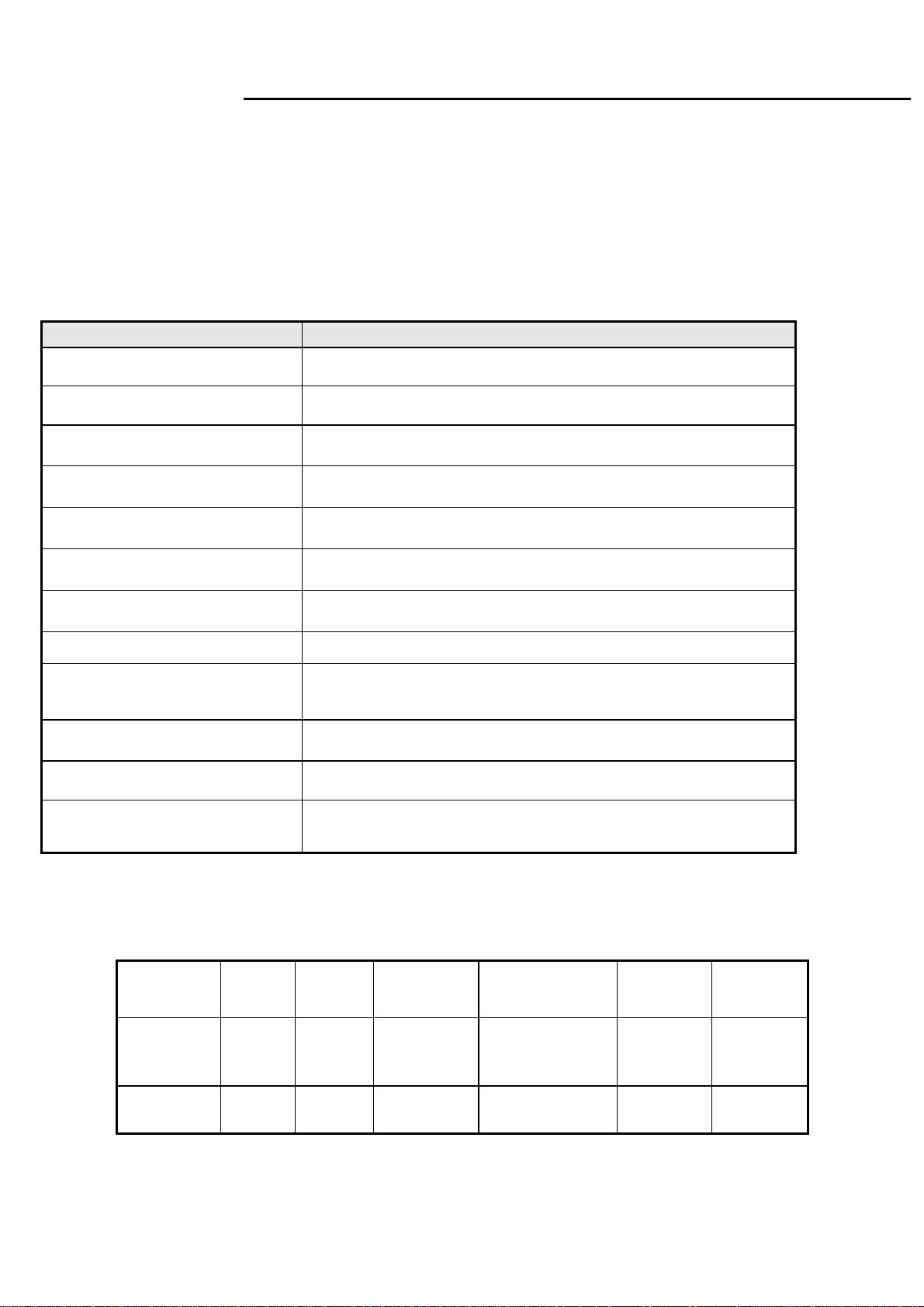
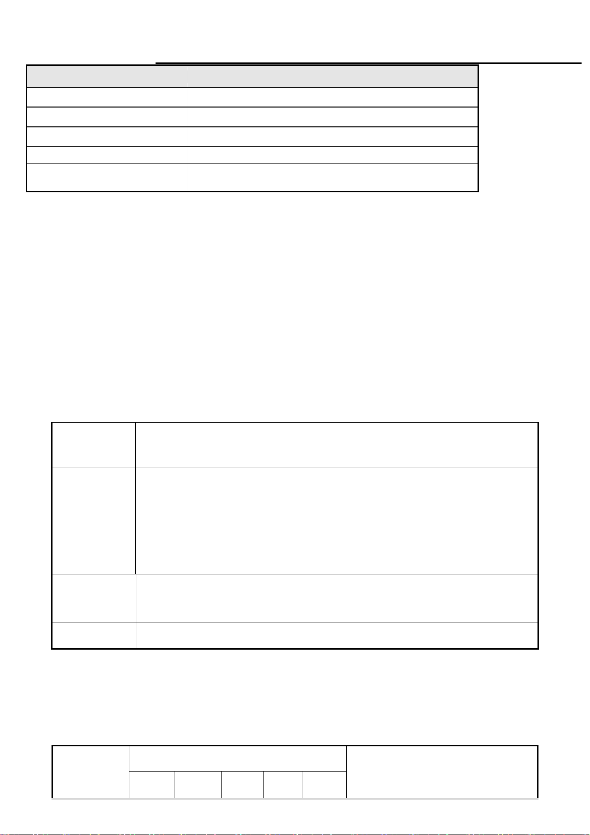
01 Product Specification
1. General:
MW22 series LCD monitor is designed with a wide screen 22” WSXGA+ TFT LCD panel, LVDS interface, RGB analog and digital
input(option).
It featured with embedded universal AC power supply. This monitor can support maximum resolution up to 1680x1050@60Hz.
1.1 Main Features
1.1.1 For SEC LTM220MT05 panel
Features Specifications
Maximum resolution
Back light system 2 CCFL
Actual Resolution display WSXGA + resolution(1680x1050)
Pixel pitch
Display area 473.76mm(H)x296.1mm(V)
Contrast ratio 600:1(min.),1000:1(typ.)10000:1(DCR)
Response time (Tr+Tf) 5ms(Typ.),8ms(Max)
Viewing angle
Input interface
Power management Compatible with VESA DPMS, Energy Star
Plug & Play VESA DDC/CI
1680x1050@60Hz
0.282mm(H)x0.282mm(W)
80°(L)/ 80°(R),80°(U)/80°(D) typ. (CR>=10)
Analog(D-sub 15pin);
Digital Optional (DVI-D with HDCP function)(option).
OSD language
English,French,Italian,Finnish,Spanish,German,Dutch,Russian
1.2 Accessories
AC
Items
Description 1.8m 1.8m 1.8m 1.8m Multi
Power
Cord
● ● ● ● ● ●
VGA
cable
Audio cable
3
DVI_D
Cable(option)
User’s
manual
Warranty
card
Page 5
MW22
Service Manual
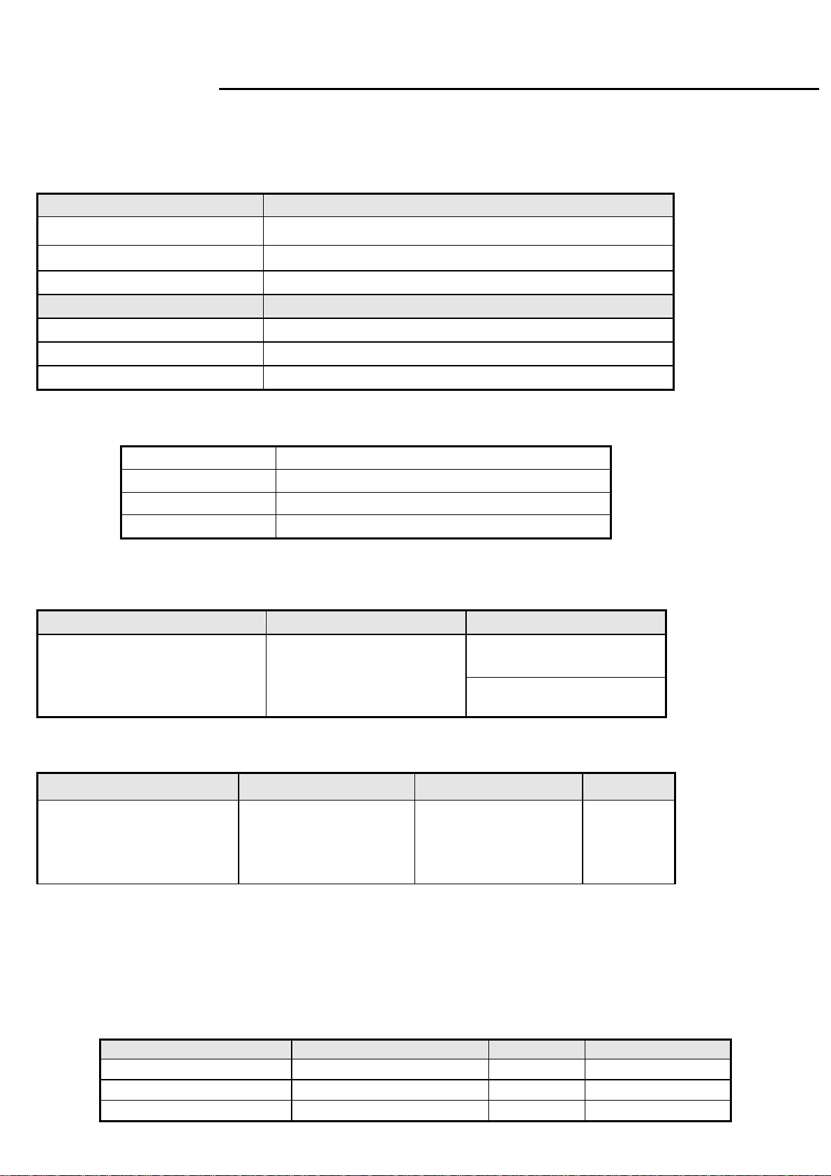
2. Operation Specifications
The unit should suffer no visible cosmetic damage and should operate with no degradation in display quality during
exposure to the operating conditions and after exposure to the non-operating conditions, in any sequence.
2.1 Environmental conditions
Operating Specification
Temperature range
Relative humidity 20% to 90%
Altitude 0 to 3048 M (10000 ft)
Storage
Temperature range
Relative humidity 10% to 90%
Altitude 0 to 12192M (40000 ft)
0°C to 50°C
-20°C to 60°C
2.2 Safety, EMC, Ergonomics and Compatibility Requirements
Safety & EMC
Ergonomics
Compatibility
Power Management
CB, VCCI, FCC-B, CCC, ,MET
MPRII, ISO-13406-2,
Windows 98/Me/2000, Windows XP, Window Vista
Energy Star
2.3 Electrostatic Discharge Requirements
Item Remark Spec
Contact discharge : ±8KV
Electrostatic Discharge
Air discharge : ±15KV
2.4 Reliability
Items Condition Spec Note
Temp: 25+/-2℃
CCFL Life time
Current: 7mA
Brightness: ≥50%
≧ 50,000 Hours
3. Electrical and Optical Characteristics and Performance
3.1 Main Power Supply
3.1.1
Input characteristics
Items Condition Spec Note
AC Input Voltage range Universal input full range 90~264Vac
AC Input Voltage rating Universal input full range 100~240Vac
AC input frequency range 90~264Vac 47~63Hz
Excluding the
LCD, CCFL
4
Page 6
MW22
A
Service Manual
AC input frequency rating 100~240Vac 50~60Hz
100Vac 1.2A
AC Input Current
240Vac 0.6A
Inrush Current
Regulator Efficiency
100 V AC cold star,25°C <35A
240 V AC cold star,25°C <70A
DC output full loading ≥80%
Note 1: Before each test, the buck capacitor needs to be discharged.
Before each test, it must be 10 minutes at least after the latest test.
Hot star not component be damaged.
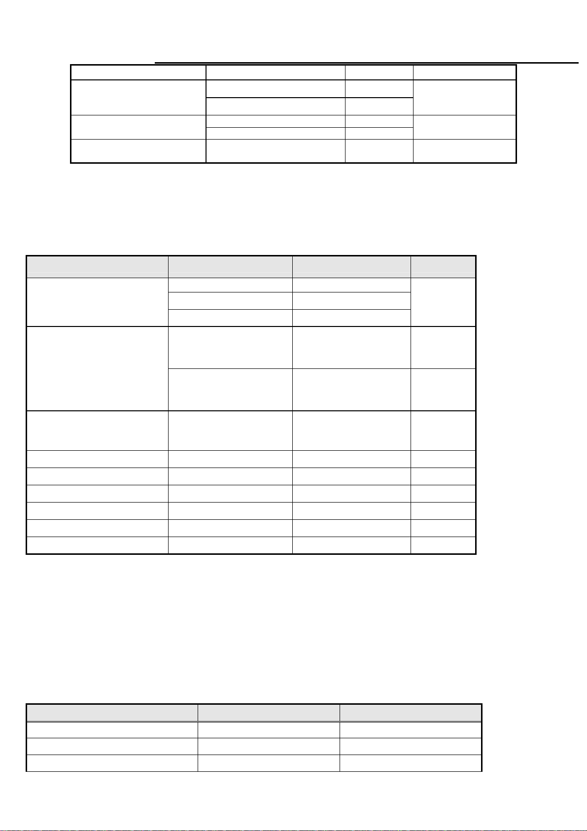
3.1.2 Output characteristics
Items Condition Spec Note
Ripple and Noise
DC Output Voltage
5v loading:0.04A~1.5
DC output loading capability
Rise Time
Dynamic load change
Hold-up time
Overshoot
Turn on delay time
+24V output <1000mv
+5V output <200mv
audio 5V output <300mv
24v loading:0.1A~0.7A
5v loading:0. 7A~1.5A
audio 5v loading:0A~1.0A
14V loading: 0A
audio 5v loading:0A
Vcc5V/1.5A
<50mS
AC input: 100V~240V >10mS
<10%
<2S
Vcc24V:23V~28V
Vcc5V:4.85V~5.35V
audio 5v:4.5V~5.5V
Vcc24V: 23V~30V
Vcc5V: 4.85V~5.35V
audio 5v:4.5V~5.5V
Vcc24V/0.7A
audio 5V/1.0A
See Note1
active
off
See note 2
For system
For power
saving or DC
Power management See Table-1
Note 2: Tested by DC loading side parallel with a 47uF/EC and 0.1uF/Ceramic Capacitors and measured band-width with
DC-20MHz.
DC 24V ripple =2400mV when inverter enters Burst Mode.
3.1.3 Protection characteristics
Protection Condition Spec
OPP nominal AC input 55W ( min )
SCP(short circuit protection) Before fuse with auto-recovery function
OVP(Over voltage protection) Auto recovery <output capacitor voltage
5
Page 7
MW22
Service Manual
Table-1
Status
Power On(with audio)
Power Saving
Power Off -- -- -- < 1W Off
H-sy
nc
3.2 Backlight Power Supply
Items Specification
V-s y
nc
on on active ≤40W Blue
off on blanked < 2W Amber
on off blanked < 2W Amber
off off blanked < 2W Amber
Video Power LED
Panel
Lamp 2 CCFL
Input Voltage DC 23~28 V
Input current 0.55A (Typ.), 0.7A (Max.)
On/Off switch level
Brightness PWM Duty (ACM Off)
Brightness PWM Duty (ACM On)
CCFL operating Voltage 760Vrms (Typ.),
CCFL Current
SEC LTM220MT05 panel
5.5V≧Von≧ 2.0 V (on)
-0.3v ≤ Voff ≤ 0.8 V (off)
30%~100%
10%~100%
2.0 mA (min.)
7.5mA (Typ.)
8.0 mA (Max.)
CCFL startup voltage
Operating frequency 40~60KHz
Protect delay time > 1 second
Efficiency ≥70% (Using dummy load)
≧1700 Vrms (0˚C)
3.3 Input / Output Signal Specifications
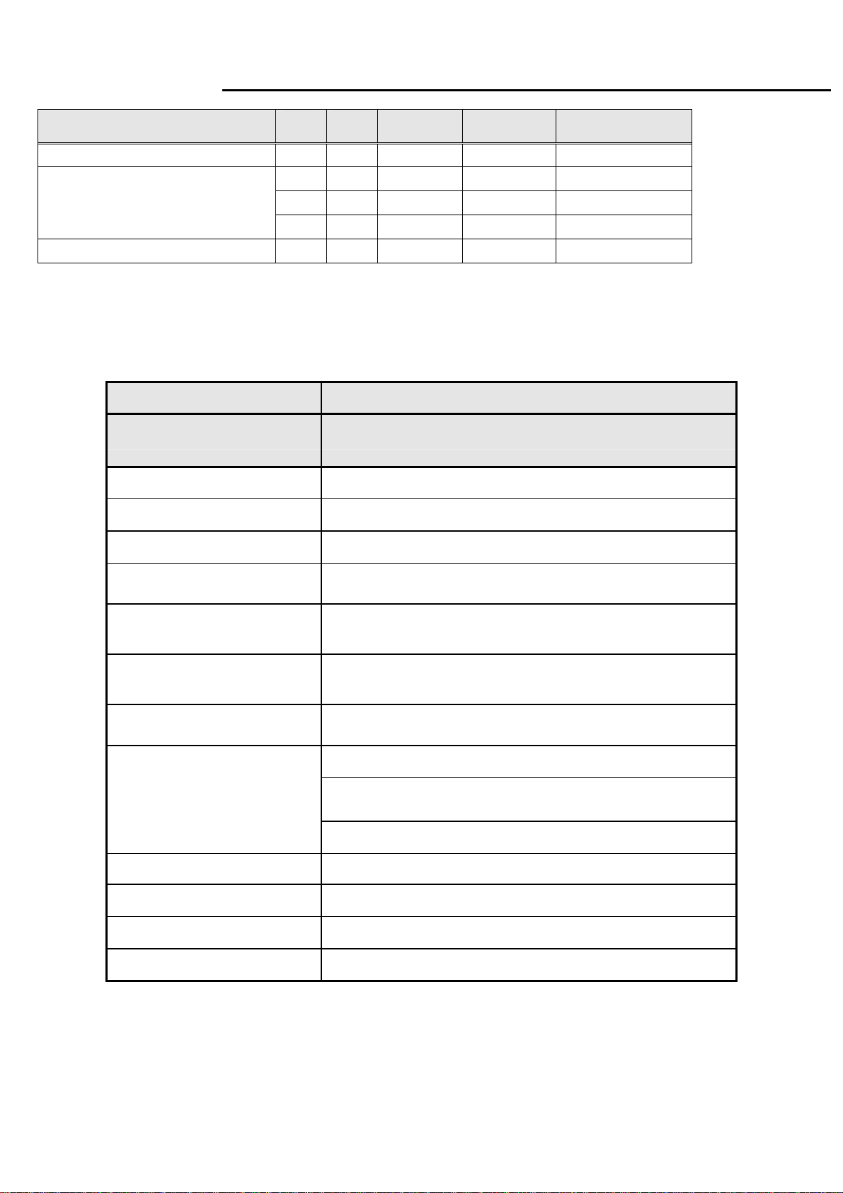
3.3.1 Video signals
6
Page 8
MW22
Service Manual
Items Condition Spec OK
Signal Cable
Analog
Digital(option)
15 pin D-Sub
DVI-D(option)
Color: BLACK
Length: 1800
Color: BLACK
Length: 1800
+/-
+/-
20 mm
20 mm
Signal type Separate analog R,G,B
Level 700 mV +/- 5% (peak to
peak)
Impedance 75 Ohms +/- 2% Ohms
Base on TMDS technology
Monitor side should be
●
blue right angle.
NO DVI cable in carton
For 15 pin D-sub
●
●
●
●
Note
Signal type Separate H/V-sync
For 15 pin D-sub
●
(Positive/Negative)
Sync
Level Logic High: 2.0V ~ 5.5V
Logic Low: 0V ~ 0.8V
Refer to VESA VSIS
●
Standard V1R1
(TTL level)
Termi nal
≧
2.2k
Ω
●
Ω
for application
2.2K
3.3.2
Signal Timing
Through D-SUB and DVI(option) connectors, this unit can support FH= 31~83 KHz, Fv=56~76 Hz.
Modes details as below:
VESA MODES
Horizontal Vertical
Mode Resolution
640*480@60Hz 31.469 N 59.941 N 25.175
Nominal
Frequency
+/-0.5KHz
Sync
Polarity
Nominal
Frequency
+/-1Hz
Sync
Polarity
Nominal Pixel
Clock (MHz)
640*480@72Hz 37.861 N 72.809 N 31.5
VGA
SVGA
XGA
SXGA
WXGA
640*480@75Hz 37.5 N 75 N 31.5
800*600@56Hz 35.156 P 56.25 P 36
800*600@60Hz 37.879 P 60.317 P 40
800*600@72Hz 48.077 P 72.188 P 50
800*600@75Hz 46.875 P 75 P 49.5
1024*768@60Hz 48.363 N 60.004 N 65
1024*768@70Hz 56.476 N 70.069 N 75
1024*768@75Hz 60.023 P 75.029 P 78.75
1152*864@75Hz 67.5 P 75 P 108
1280*960@60Hz 60 P 60 P 108
1280*720@60Hz 44.955 P 59.94 P 74.176
1280x1024@60Hz 63.981 P 60.020 P 108.000
1280x1024@75Hz 79.976 P 75.025 P 135.000
1280*800@60Hz 49.702 N 59.810 P 83.500
7
Page 9
MW22
Service Manual
1360x768@60Hz 47.712 P 60.015 P 85.500
1440x900@60Hz 55.935
WXGA+
WSXGA+
VGA
SVGA
XGA
Note: 1. Non-interlace signals only (An interlace signal cannot be display)
2. Please refer to F/W specification for more detail
3. Each frequency of Power Macintosh and Sun Ultra is a reference value
3.3.3
Timing requirements
1440x900@75Hz 82.306
1680*1050@60Hz 65.290 N 59.954 P 146.250
IBM MODES
720x400@70Hz 31.469 N 70.087 P 28.322
MAC MODES
640*480@66.7Hz 35 P
832*624@74.55Hz 49.722 N 74.55 N 57.283
1152*870@75Hz 68.681 N 75.062 N 100
N
N
59.887
74.892
66.667 N 30.24
P
P
106.500
187
Item Condition Specification
Horizontal
Vertical
Out of range
3.3.4
DDC data
Sync polarity: (+) or (-)
Sync polarity: (+) or (-)
Excluding Horizontal
(31~83)KHz or
Vertical 56~76 Hz
31~83KHz
56~76 Hz
Message “
EDID Standard Compliance
EDID File Format : VESA’s EDID Standard Version #3, Revision #0,
EDID Structure : Version #1, Revision #3.
EDID Data Table : See the file of LE22T9-DR4-16
4. LCD Characteristic & Performance
4.1 Panel general specifications
Frequency out of range” on screen
General Specifications
(1) The test methods for the below items’ definition, please refer to the specification of SEC LTM220MT05 panel
Supplier SEC
Model name LTM220MT05
Display Area 473.76mm(H)x296.1mm(V)
Pixel Pitch 0.282mmx 0.282mm
Display Colors: 16.7Million (Hi-FRC)
8
Page 10
MW22
Service Manual
Number of Pixel 1680x1050 pixels
Pixel Arrangement RGB vertical stripe
Brightness 250cd/m2 (Typ.)
Contrast Ratio 1000:1 (Typ.)
Viewing Angle Hor:160°, Ver: 160°(Typ)
Brightness Uniformity
Display Mode Normally White
Response Time(Tr+Tf) 5ms (Typ.), 8ms (Max.)
Surface Treatment Haze 25%, Hard-coating (3H)
Lamp 2 CCFL
Notes: Other panel source, please refer to the panel specifications.
≧75%
4.2 Optical characteristic of LCD panel
(1) The test methods for the below items’ definition, please refer to the specification of SEC LTM220MT05panel.
Item Unit Conditions Min. Typ. Max. Remark
Viewing Angle
Contrast ratio
Response Time
Color / Chromaticity
Coordinates (CIE)
Color Coordinates (CIE) White
Luminance Uniformity
White Luminance at
CCFL 6.5mA(center point)
[degree]
[degree]
[degree]
[degree]
Normal Direction 600 1000
[msec] Rising Time -
[msec] Falling Time -
[msec] Rising + Falling - 5 8
Red x
Red y 0.305 0.330 0.355
Green x 0.275 0.300 0.325
Green y 0.575 0.600 0.625
Blue x 0.125 0.150 0.175
Blue y 0.035 0.060 0.085
[%] 9 points measurement 75%
[cd/m2]
Horizontal (Right)
CR >= 10 (Left)
Vertical (Up)
CR >= 10 (Down)
White x 0.288 0.313 0.338
White y 0.304 0.329 0.354
250 -
70
70
70
70
0.615
80
80
80
80
0.640
-
-
-
-
0.665
4.3 Brightness output
The test to verify specifications in this section shall be performed under the following standard conditions unless otherwise
noted.
Temperature : 25 ± 5°C
Test pattern : white
Video Resolution : 1680x1050
Video input level : 700 mV ± 2%
Warm-up time : 30 minutes
9
Page 11
MW22
Service Manual
Item Condition SPEC
Brightness
Grey Scale
4.4 White balance
The test standard conditions refer to Sec 3.3. (Brightness control is at 100 contrast control is at 50.)
Brightness=100%
Contrast = 100%
Brightness=100%
Contrast = 100%
≧ 200 cd/m
the last 3~8 levels of 32
grey scales is combined
2
Cool
Warm
User
4.5 Brightness uniformity
The test standard conditions refer to Sec 3.4.
Mode
9300K 0.283 ± 0.030 0.297 ± 0.030
6500K 0.313 ± 0.030 0.329 ± 0.030
Panel While x Panel While y
)(backlight points nine of luminance Min.
≥
)(backlight points nine of luminance Max.
L/2
4 6
Chromaticity Coordinate
x y
(4)
%75
L/10
5
W/10
1 2
7
8
3
9
W/2
Fig.3
4.6 Audio Signal
10
Page 12
MW22
Service Manual
Items Specification
Input impedance
Frequency response range
Signal to noise ratio
Output power
Loading impedance
Note: The low pass RC Filter (R=100Ω / C=0.047uF) for Class-D output power and THD+N measurement, and under 1KHz, 1Vrms
and sine wave input.
≧ 10K ohm
200Hz –20kHz
≧ 40 dB
≦1 W + 1 W(±20% tolerance), THD 10%.
4 ohm
5. Function Specifications
All the tests to verify specifications in this section shall be performed under the following standard conditions unless
otherwise noted. The standard conditions are:
Temperature : 25 ± 5°C
Warm-up time : 30 minutes minimum
Checking display modes : All the specified modes
5.1 Keypad Function
5.1.1
注:1.if current Menu is Language menu, when you press
[AUTO] key, it will not save your select and
Control buttons
A. When OSD un-displays , press [AUTO] to perform auto-adjustment
[AUTO]
[MENU]
[>], [<]
[POWER] Power on or power off the monitor
B. When OSD displays, and the current Menu is Main Menu press [AUTO] to turn off the
Main Menu, or press [AUTO] to return to previous level menu.
A. When OSD isn’t shown on screen, press [MENU] to enter OSD interface.
B. When OSD displays, press [MENU] to perform function of menu icon that is highlight or
enter next level menu, and if the Menu is the last layer of OSD press [MENU] to finish
adjust and turn off Menu.
A. When “MENU OSD” displays, press these keys to change the contents of an
adjustment item, or change an adjustment value.
B. When “MENU OSD” un-displays, press [<] to show “Audio” OSD, press [>] to show
“Theme Mode” OSD.
return to
[MENU]
previous menu.
key, it will save your select and return to
previous menu. and when you press
5.1.2
Hot Key Operation
HOT KEY OPERATION
FUNCTION
AUTO MENU <
>
11
POWER
DESCRIPTION
Page 13

MW22
Service Manual
Press [AUTO] at the same time, and then press
FACTORY
MODE
●
ON
[POWER] for DC power on. OSD menu will be
shown with “F” on the left top. Select “F” for
entering factory mode
Volume
Theme Mode
●
●
Adjust Volume
Select Theme Mode
12
Page 14
MW22
Service Manual
5.2 OSD Structure
The On-Screen Display (OSD) shall be an easy to use icon based menu through keypad OSD buttons or remote control
unit. The unit shall leave the factory with all OSD controls set to their default values.
Analog:
“Picture” will be the first selected function while user power on main menu.
First Second Third Fourth Control Value Default
Auto
VGA
Input
Audio Volume 50
Picture
Geometry
Advanced
DVI
Brightness 80
Contrast 50
Gamma
H-Position 50
V-Position 50
Clock 50
Phase
Color
Language
Resolution
Reminder
Information
Enable Reset
Disable
Gamma2.0
Gamma2.2
Gamma2.4
Warm Default color
Cool
Customer
Color
Theme Mode
English
Français
Italiano
Español
Hollands
Русский
Suomalainen
Deutsch
Gamma 2.2
Red 50
Green 50
Blue 50
Movie
Game
Picture
User
Tint/Hue 50
Saturation 50
Sharpness 50
Dynamic
Enable
Disable
English
Disable
Disable
13
Page 15
MW22
Service Manual
DVI(option):
If our monitor is in Dual mode, the gray area below will be the function which could not be adjusted.
First Second Third Fourth Control Value Default
Auto
VGA
Input
Audio Volume 50
Picture
Geometry
Advanced
DVI
Brightness 80
Contrast 50
Gamma
H-Position
V-Position
Clock
Phase
Color
Language
Resolution
Reminder
Information
Enable Reset
Disable
Gamma2.0
Gamma2.2
Gamma2.4
Warm Default color
Cool
Customer
Color
Theme Mode
English
Français
Italiano
Español
Hollands
Русский
Suomalainen
Deutsch
Disable
Gamma 2.2
Red 50
Green 50
Blue 50
Movie
Game
Picture
User
Tint/Hue 50
Saturation 50
Sharpness 50
Dynamic
Enable
Disable
English
Disable
14
Page 16
MW22
Service Manual
Theme Mode Brightness Contrast
Movie 100 54
Game 100 58
Picture 100 50
User(After Reset all) 80 50
Remark:
1. Main OSD will Show 10 Second on the Screen,if there is No Operation on the OSD,And ±1 Second is accepted.
2.Gamma 2.0(2.0±0.2), Gamma 2.2(2.2±0.2), Gamma 2.4(2.4±0.2).
3. When dynamic be enabled, after adjusting theme mode/Color Menu, DCR function will be turn off automatically.
5.3 Gateway OSD Message
Item Description
When User Press Hot-Key “Auto” or use main Menu “Auto processing”
Auto Processing
No Signal
Frequency out of
range
Resolution
Reminder
function, will show this message ,and the monitor do the auto process
function.
When the video cable is connect, but there is no active signal input, will
show this message, then enter into power saving mode.(will Show 3
seconds)
1. When meet the case as below:
a. Input signal is detected by the system;
b. Input signal is out of the system support rang or supported table which
may have following case:
-input signal is out of the support H or V frequency range;
-input signal is in specified blocked list;
-Input signal is out of the system support specification;
Then will show this message.
2. The menu will be shown as:
a. Move around the full screen;
b. Desktop background in Black;
c. Continue 5 minutes and then step into Power Saving Mode.
When user entering into “Advanced” menu, user could select “Resolution
reminder” item. After selecting “Resolution reminder”, main menu will show
“Your Computer screen resolution may not match this monitor’s optimum
1600x900 setting. To adjust your screen resolution and see your
computer’s printed or online documentation. Press the AUTO button on the
side of this monitor after adjusting the screen resolution. ”
Information
Reset
Input Menu
While user entering into “Advanced” menu, user could select “Information”.
Main menu will show “Mode:, Input: , OSD Vers: ,SN ”.
Go to “Main menu” and select “Reset” function. After select “Reset”,
monitor will show a “Reset All” pop up window.
This Menu will Show at the Cases Below(3 Seconds) :
1. AC/DC On;
2. Power Saving On;
3. Burn In On;
4. Switch Source;
5. Plug and pull out Cable.
15
Page 17
MW22
Service Manual
6. SOP of PCBA ISP Programming
6.1 Operational condition:
Equipment: PC, ISP card, signal cable and power cable.
ESD requirements: antistatic wrists, antistatic gloves(fingers), and connecting cable
Name of ISP program: ISP_Tool_V4.4.2.4
Manufacture of FW IC:PMC/SST/MX
6.2 Operational steps:
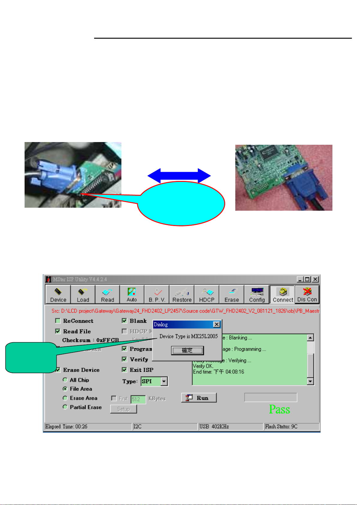
1. Connection: connect PC to PCBA with signal cable, and then keep AC and DC in open state.
Signal cable
One port of ISP
program card is
connected to
PC
2. Adjust ISP programming
Firstly, double click ISP_Tool_ V4.4.2.4 exit and click “Connect ” button; The ISP tool will connect to
monitor automatically, and it will show flash IC type automatically
FW IC
Model
16
Page 18
MW22
Service Manual
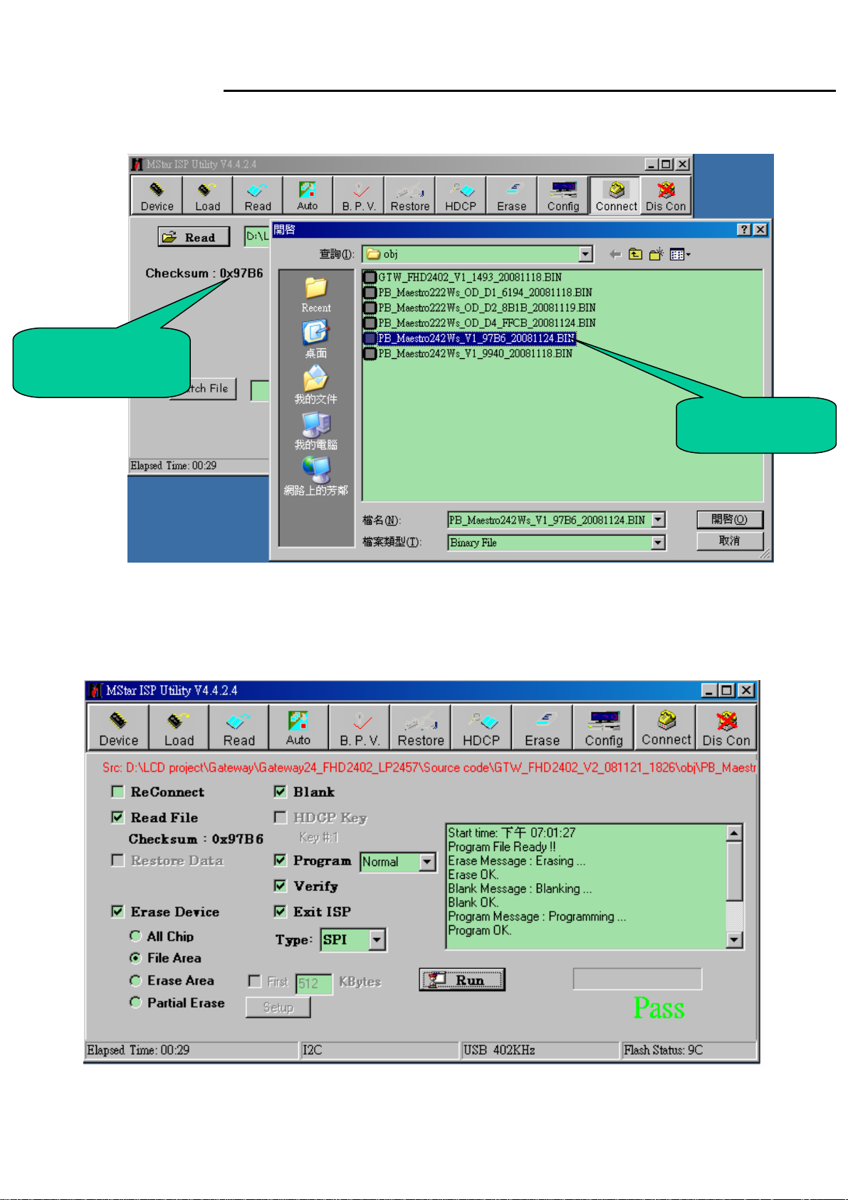
Secondly﹐download FW software: first select “READ”, and then load FW software in Rooter
(Fig.2).
Software
Checksum value
FW BIN file
Thirdly, select “AUTO”, and keep its default value. Click “RUN” for beginning programming. There will
be prompting if programming is OK.
17
Page 19
MW22
Service Manual
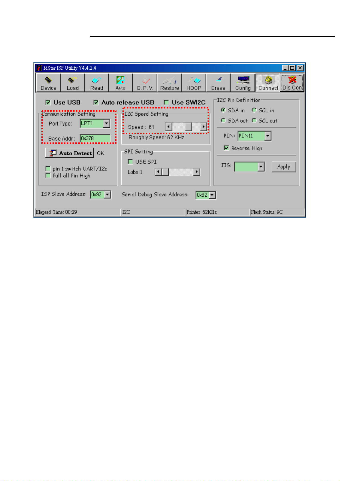
◆Note: if programming fails or success rate is not high, click “Config” and adjust its speed to lower
in “I2C Speed Setting”and check Communication Setting. If connect port is print port, please check
port type.
18
Page 20
MW22
Service Manual
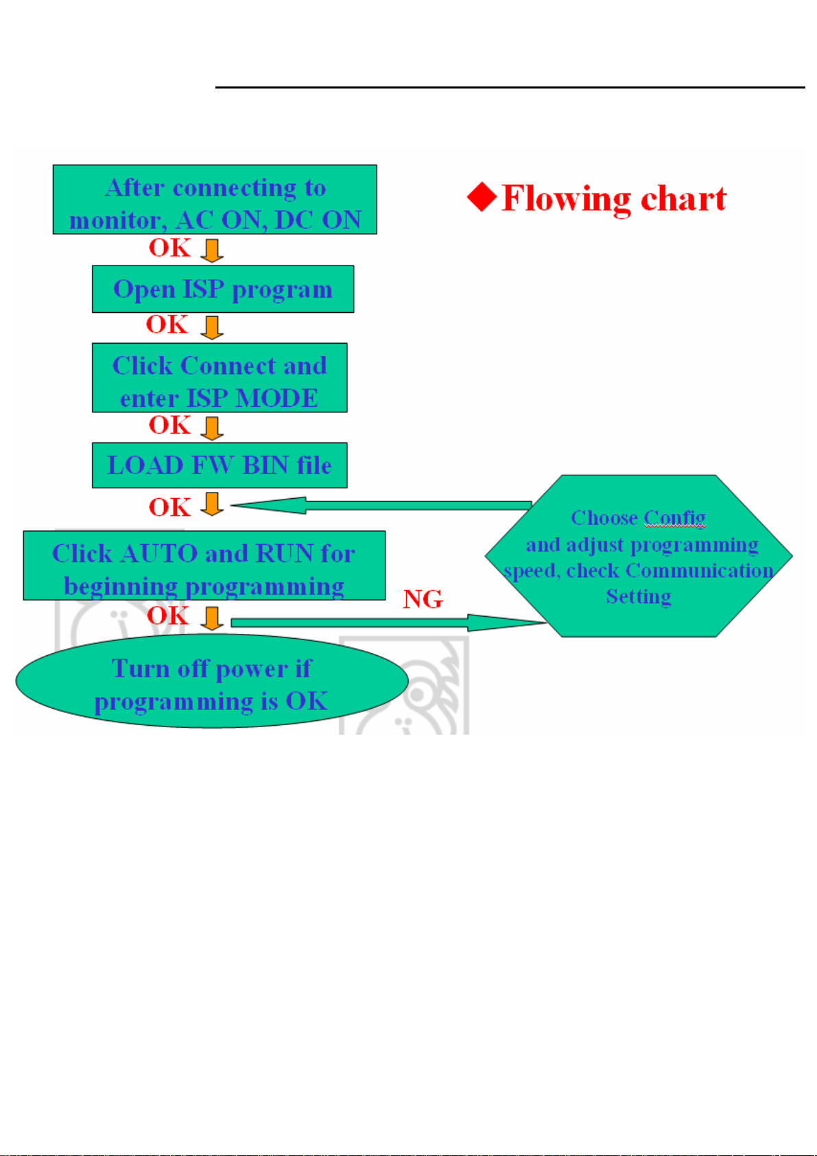
3. Flow Chart
19
Page 21
MW22
Service Manual
7. SOP of EDID
7.1 Request of hardware and software:
1. Software
a.port95nt.exe
b.Edid.exe
c.MW22 model
2. Hardware
a. PC(winXP or win2000)1PCS;
b. Tool(EDID Card、VGA cable & DVI cable)
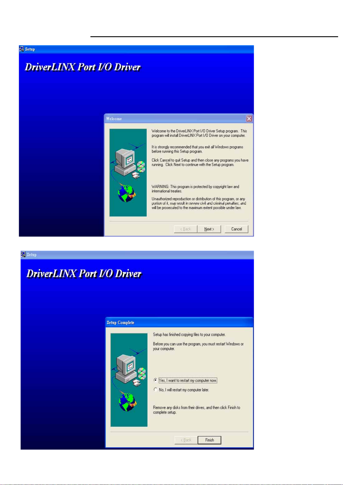
7.2 Operational steps:
1. First set up Port95nt.exe
20
Page 22
MW22
Service Manual
2. Click next button continually then can finish setting.
21
Page 23
MW22
Service Manual
EDID Tool Set up
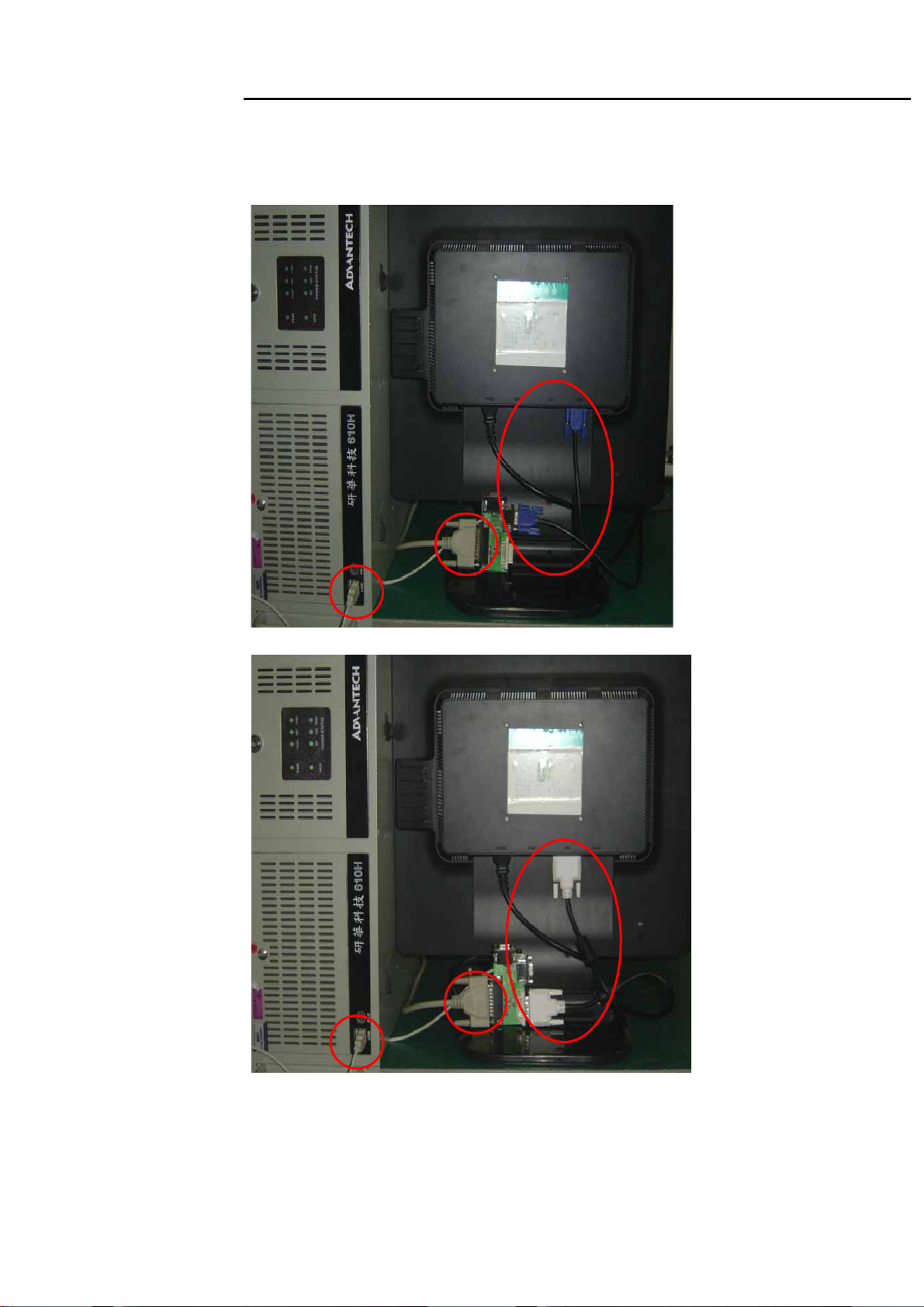
A : USB interface provide +5V DC power(No Power is ok )
B : Connect DDC Card and PC with collateral interface ;
C :VGA、DVI use different cable to link DDC and PC
A
A
B
B
C
C
22
Page 24
MW22
B C
Service Manual
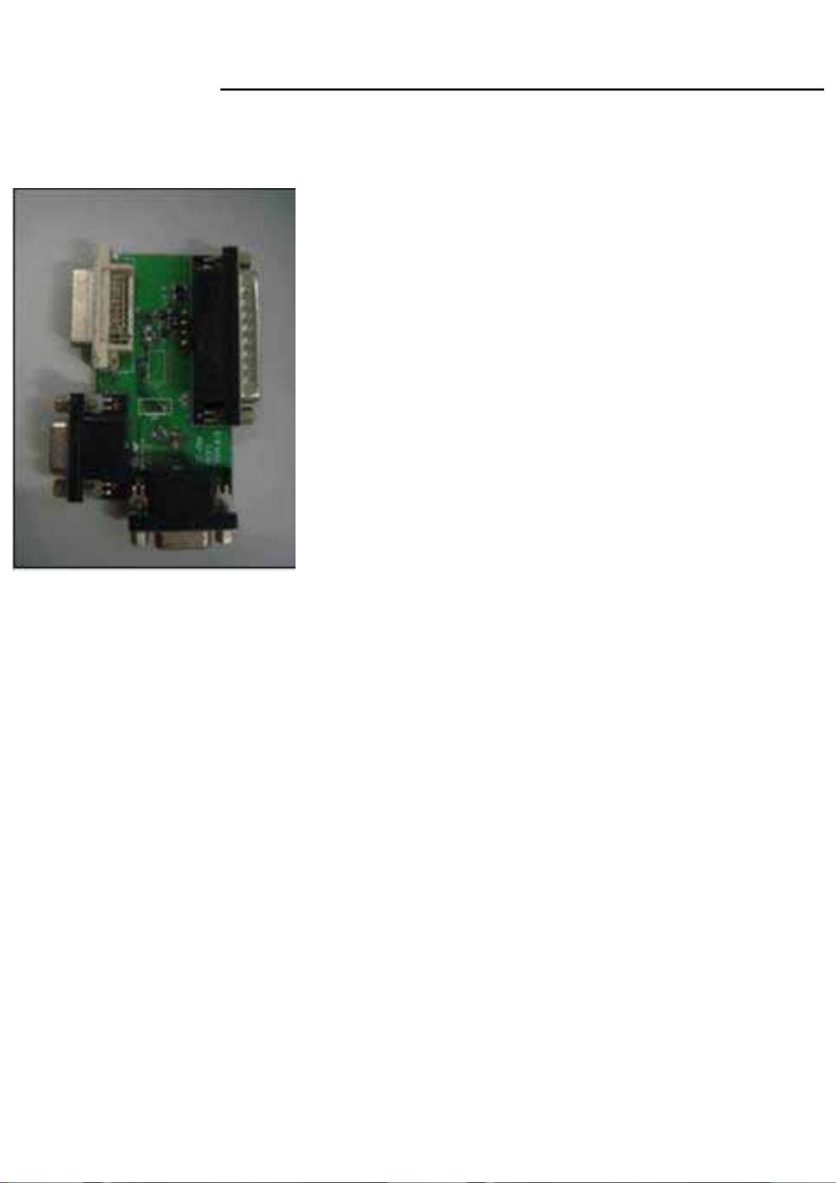
EDID ISP Card:
A
A:Collateral printing interface (connect with PC)
B : VGA interface (one VGA connect with PC to provide signal for monitor the other one connect with
PC VGA interface to write VGA EDID, Write EDID can without providing signal)
C : DVI interface (connect with Monitor)
23
Page 25
MW22
Service Manual
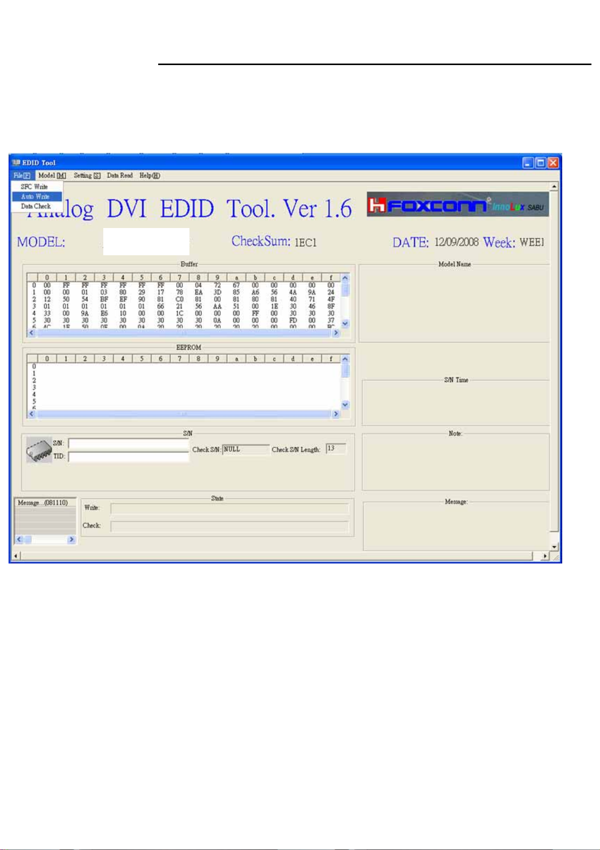
3. Write EDID Process:
3.1 Choose File menu in main menu ,choose Auto Write button,click S/N blank .
MW22
24
Page 26
MW22
Service Manual
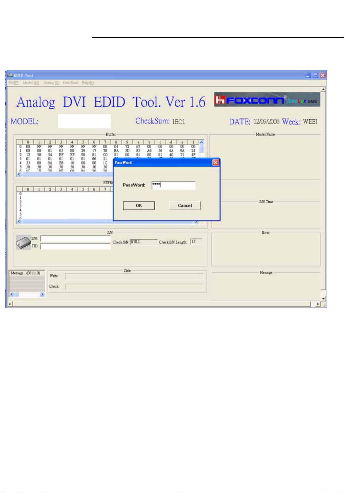
3.2 Cloose the Model in main menu, and the password is 1234.
MW22
25
Page 27
MW22
Service Manual
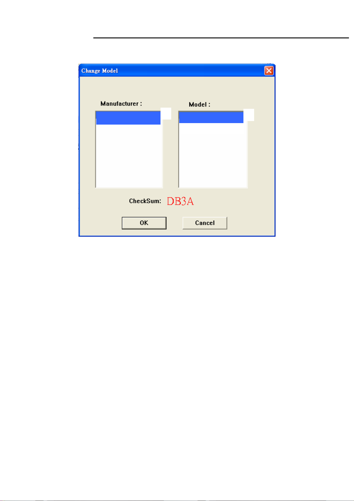
3.3 Choose the model, MW22_A(Update VGA) ,MW22_D(Update DVI) .
MW22
MW22_D
MW22_A
26
Page 28

MW22
Service Manual
3.4 Input S/N in the Blank , eg:ETLA10C109805111D94023,the program can write directly.
MW22
27
Page 29

MW22
Service Manual
3.5 After the process is ok , the program can check that automatically
MW22
28
Page 30

MW22
Service Manual
3.6 If write successfully , you can see PASS in the right
MW22
MW22
29
Page 31

MW22
Service Manual
02. Flat Panel Specification
30
Page 32

Mechanical Information
Approval Specification
Approval Specification
Module
size
Max.
494.2
320.6
17.0
2,600
mm493.7493.2Horizontal (H)
mm320.1319.6Vertical (V) w/o inverter ass’y
mm--Depth (D)
NoteUnitTyp.Min.Item
LCD module onlyg--Weight
Note (1) Mechanical tolerance is ± 0.5mm unless there is a special comment.
1. Absolute Maximum Ratings
If the condition exceeds maximum ratings, it can cause malfunction or unrecoverable
damage to the device.
Power Supply Voltage
Data Signal
Storage temperature
Center of Glass surface temperature
(Operation)
Shock ( non - operating )
Vibration ( non - operating )
Note (1) Ta= 25 ± 2 °C
DD
sig
STG
OPR
nop
nop
NoteUnitMax.Min.SymbolItem
(1)V6.5GND-0.5V
V5-V
60-25T
500T
℃
℃
(2)
(2)
(3)(5)G50-S
(4)(5)G1.5-V
5/39Page05-000-G-080902Doc. NoLTM220MT05MODEL
Page 33

Approval Specification
Approval Specification
(2) Temperature and relative humidity range are shown in the figure below.
a. 90 % RH Max. (Ta ≤ 39 °C)
b. Maximum wet-bulb temperature at 39 °C or less. (Ta ≤ 39 °C)
c. No condensation
(3) 11ms, sine wave, one time for ±X, ±Y, ±Z axis
(4) 10-300 Hz, Sweep rate 10min, 30min for X,Y,Z axis
(5) At vibration and shock test, the fixture which holds the module to be tested has to be
hard and rigid enough so that the module would not be twisted or bent by the fixture.
(39,90)
(39,90)
(50,50.4)
(50,50.4)
25,5)
((--25,5)
Fig. Temperature and Relative humidity range
(60,27.7)
(60,27.7)
6/39Page05-000-G-080902Doc. NoLTM220MT05MODEL
Page 34

Approval Specification
2. Optical Characteristics
Approval Specification
The optical characteristics should be measured in a dark room or equivalent.
Measuring equipment : SR-3, RD-80S (TOPCON), EZ-Contrast (Eldim)
(Ta = 25 ± 2°C, VDD=5V, fv= 60Hz, fDCLK=59.6MHz, IL = 7.5mArms)
NoteUnitMax.Typ.Min.ConditionSymbolItem
Contrast Ratio
(Center of screen)
Response
Time
Luminance of White
(Center of screen)
Green
Color
Chromaticity
(CIE 1931)
Blue
White
Red
Red
-1000600C/R
85-Tr + TfOn/Off
L
Normal
=0
θ
L,R
θ
=0
U,D
Viewing
Angle
-250200Y
0.6700.6400.610Rx
0.3600.3300.300Ry
0.3300.3000.270Gx
0.6300.6000.570Gy
0.1800.1500.120Bx
0.0900.0600.030By
0.3430.3130.283Wx
0.3590.3290.299Wy
-0.451-Ru'
-0.523-Rv'
msec
cd/m
2
(3)
SR-3
(5)
RD-80S
(6)
SR-3
(7),(8)
SR-3
Color
Chromaticity
(CIE 1976)
C.G.L
(ACC ONLY)
* C.G.L : Color Grayscale Linearity
Green
Blue
White
△u'v'White
-0.125-Gu'
-0.564-Gv'
-0.175-Bu'
-0.158-Bv'
-0.198-Wu'
-0.468-Wv'
(9)0.02--
7/39Page05-000-G-080902Doc. NoLTM220MT05MODEL
Page 35

Approval Specification
Approval Specification
NoteUnitMax.Typ.Min.ConditionSymbolItem
K-6500--Color Temperature
θ
Hor.
Viewing
Angle
Ver.
Brightness Uniformity
(9 Points)
L
θ
R
θ
U
θ
D
uni
Note (1) Test Equipment Setup
The measurement should be executed in a stable, windless and dark room between
30min after lighting the back light at the given temperature for stabilization
of the back light. This should be measured in the center of screen.
Single lamp current : 7.5mA
Environment condition : Ta = 25 ± 2 °C
CR≥10
-8070
-8070
Degrees
-8070
-8070
%25--B
(8)
EZ-
Contrast
(4)
SR-3
Field Photo detector
2°SR-3
TFT - LCD Module
Photo detector
Field
SR-3 : 40㎝
RD-80S : 50㎝
LCD Panel
The center of the screen
8/39Page05-000-G-080902Doc. NoLTM220MT05MODEL
Page 36

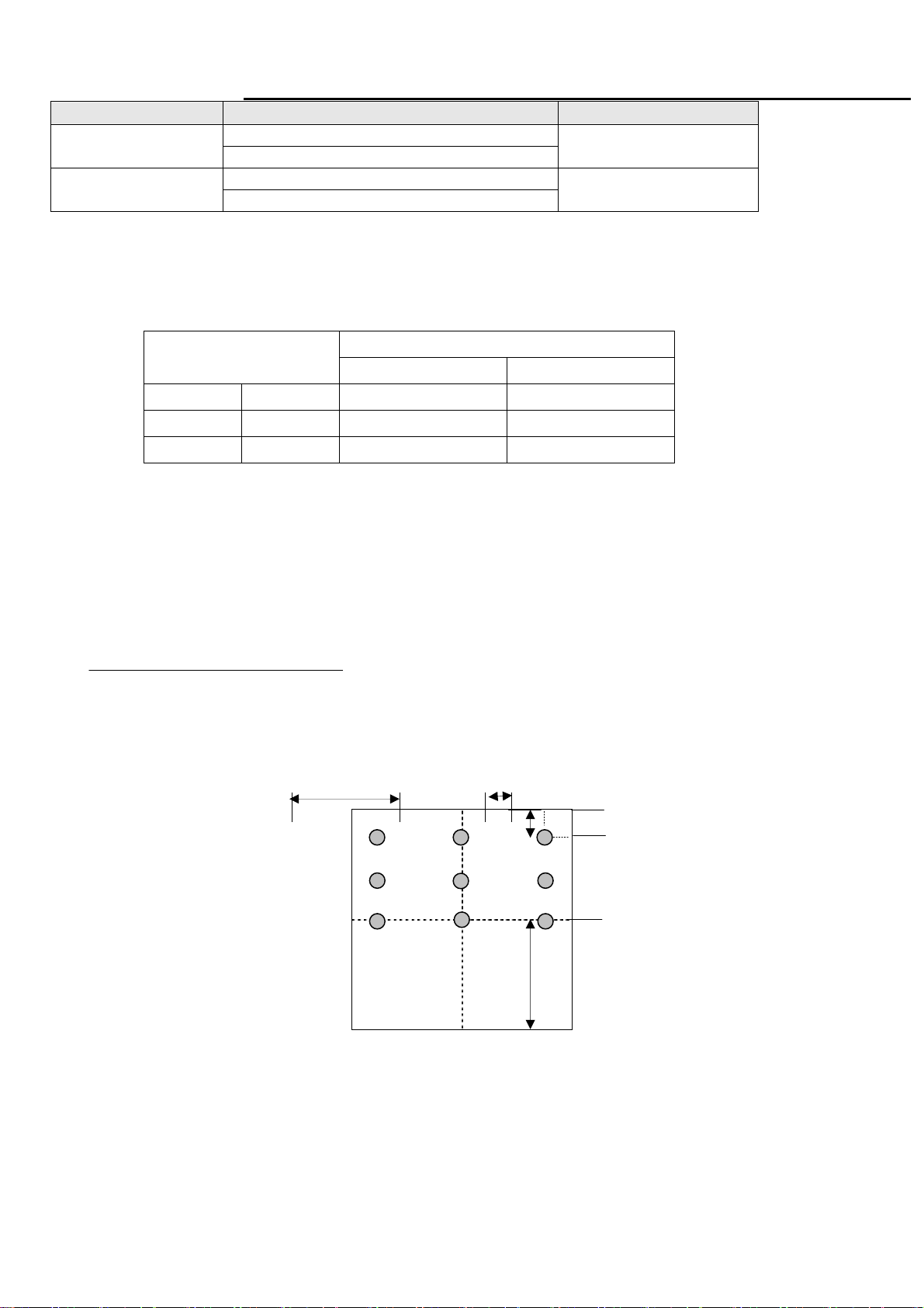
Note (2) Definition of test point
−
168 840 1512
Approval Specification
Approval Specification
Active Area
6
: Test Point
Note (3) Definition of Contrast Ratio (C/R)
: Ratio of gray max (Gmax) & gray min (Gmin) at the center point⑤ of the panel
3 2 1
G
CR
=
G
Gmax : Luminance with all pixels white
Gmin : Luminance with all pixels black
Note (4) Definition of 9 points brightness uniformity
BB
Buni
=×
(max min)
100
B
max
8 79
max
min
105
45
525
945
Bmax : Maximum brightness
Bmin : Minimum brightness
Note (5) Definition of Response time : Sum of Tr, Tf
Display Data White(TFT off) Black(TFT on) White(TFT off)
Optical Instruments
Response
100%
90%
10%
0%
9/39Page05-000-G-080902Doc. NoLTM220MT05MODEL
Page 37

Approval Specification
Approval Specification
Note (6) Definition of Luminance of White : Luminance of white at center point⑤
Note (7) Definition of Color Chromaticity (CIE 1931, CIE1976)
Color coordinate of Red, Green, Blue & White at center point⑤
Note (8) Definition of Viewing Angle
: Viewing angle range (CR ≥10)
10/39Page05-000-G-080902Doc. NoLTM220MT05MODEL
Page 38

Approval Specification
Approval Specification
Note (9) Color Grayscale Linearity
a. Test image : 100% full white pattern with a test pattern as below
b. Test pattern : Squares, 40mm by 40mm in size, filled with 255, 225, 195, 165, 135 and
105 grays steps should be arranged at the center⑤ of the screen.
c. Test method
st
-1
gray step : move a square of 255 gray level should be moved into the center of the
screen and measure luminance and u’ and v’ coordinates.
- Next gray step : Move a 225 gray square into the center and measure both
luminance and coordinates, too.
d. Test evaluation
Δu'v'= (u' -u' ) +(v' -v' )AB
Where A, B : 2 gray levels found to have the largest color differences between them
i.e. get the largest Δu’ and Δv’ of each 6 pair of u’ and v’ and calculate the Δu’v’.
2
AB
2
11/39Page05-000-G-080902Doc. NoLTM220MT05MODEL
Page 39

3. Electrical Characteristics
3.1 TFT LCD Module
The connector for display data & timing signal should be connected.
Approval Specification
Approval Specification
Ta = 25°C
NoteUnitMax.Typ.Min.SymbolItem
Voltage of Power Supply
Differential Input
Voltage for LVDS
Receiver Threshold
LVDS skew
LVDS
Input
Characteri
Differential input
voltage
stics
Input voltage range
(single-ended)
Common mode
voltage
(a) Black
Current of
Power
Supply
DD
SKEW
IN
V
CM
I
DD
|V
0+
ID
|/2
1.2
2.4-
|V
(1)V5.55.04.5V
(2)mV+100--High
mV---100Low
(3)ps300-300t
(4)mV600200|VID|
(4)V2.40V
(4)V
|/2
ID
mA-1,500mA-900-(b) White (5),(6)
mA1,9001,700-(c) Dot
Vsync Frequency
Hsync Frequency
Main Frequency
Rush Current
V
H
DCLK
RUSH
Note (1) The ripple voltage should be controlled under 10% of VDD.
Hz766053f
kHz83.264.857.2f
MHz77.559.552.6f
(7)A4.0--I
12/39Page05-000-G-080902Doc. NoLTM220MT05MODEL
Page 40

Approval Specification
Approval Specification
(2) Differential receiver voltage definitions and propagation delay and transition time test
circuit
a. All input pulses have frequency = 10MHz, t
b. C
includes all probe and fixture capacitance
L
or tF=1ns
R
Note a.
Note b.
(3) LVDS Receiver DC parameters are measured under static and steady conditions
which may not be reflective of its performance in the end application.
T
LVDS Clk
V
= 0V
DIFF
LVDS Data
RX +/-
t
SKEW
where tskew : skew between LVDS clock & LVDS data,
T : 1 period time of LVDS clock
cf) (-/+) of 300psec means LVDS data goes before or after LVDS clock.
(4) Definition of V
ID
and V
using single-end signals
CM
V
= 0V
DIFF
Differential
Differential
13/39Page05-000-G-080902Doc. NoLTM220MT05MODEL
Page 41

(5) fV=60Hz, fDCLK = 59.6MHz, VDD = 5.0V, DC Current.
(6) Power dissipation check pattern (LCD Module only)
a) Black Pattern b) White Pattern c) Dot Pattern
(7) Measurement Condition
100%
90%
Approval Specification
Approval Specification
V
DD
10%
GND
Rush Current I
T
RUSH
can be measured when T
RUSH
=470㎲
. is 470㎲.
RUSH
14/39Page05-000-G-080902Doc. NoLTM220MT05MODEL
Page 42

Approval Specification
Approval Specification
3.2 Back Light Unit
The back light unit is an edge - lighting type with 2 dual CCFTs ( Cold Cathode
Fluorescent Tube ) The characteristics of two dual lamps are shown in the following tables.
Ta=25 ± 2°C
NoteUnitMax.Typ.Min.SymbolItem
Lamp Current
Lamp Voltage
Lamp Frequency
Asymmetry
Inverter
waveform
Note (1) Specified values are for a single lamp.
Lamp current is measured with current meter for high frequency as shown below.
Refer to the following block diagram of the back light unit for more information.
rate
Distortion
rate
L
L
L
(1)mArms8.07.54.0I
Vrms-760-V
(2)kHz60-40f
(3)Hour--50,000HrOperating Life Time
%10--Wasy
(4)
1.55541.4141.2726Wdis
--VsStartup Voltage
0℃ : 1,700
25℃: 1,400
(5)Vrms
LCD Module
HOT
COLD
I
1
A
INVERTER
HOT
COLD
Fig. Measurement point of Lamp Current
I2
A
15/39Page05-000-G-080902Doc. NoLTM220MT05MODEL
Page 43

Approval Specification
−
Approval Specification
(2) Lamp frequency which may produce interference with horizontal synchronous
frequency may cause line flow on the display. Therefore lamp frequency should be
detached from the horizontal synchronous frequency and its harmonics as far as
possible in order to avoid interference.
(3) Life time (Hr) is defined as the time when brightness of a lamp unit itself becomes
50% or less than its original value at the condition of Ta = 25±2°C and IL= 7.5mArms
(4) Designing a system inverter intended to have better display performance, power
efficiency and lamp reliability.
They would help increase the lamp lifetime and reduce leakage current.
a. The measurement should be done at typical lamp current.
b. The asymmetry rate of the inverter waveform should be less than 10%.
c. The distortion rate of the waveform should be √2 with ±10% tolerance.
- Inverter output waveform had better be more similar to ideal sine wave.
Asymmetry rate
p-p
I
p
I
-p
Fig. Wave form of the inverter
(5) If an inverter has shutdown function, it should keep its output for over 1 second
even if the lamp connector is open. Otherwise the lamps may not be turned on.
||II
I
rms
Distortion rate
I
p
||
I
or
rms
× 100
I
-p
||
I
rms
16/39Page05-000-G-080902Doc. NoLTM220MT05MODEL
Page 44

4. BLOCK DIAGRAM
4.1 TFT LCD Module
RSDS
Control signal
Approval Specification
Approval Specification
Source Driver ICs
LVDS
pair #1
LVDS
pair #2
CN1
(30pin)
LVDS (Rx)
LVDS(Tx)
Timing Controller
+5.0V
V
DD
Power
Circuit
4.2 Back Light Unit
Connector: YEONHO 35001HS-02L Or Compatible
S1 S1680
Control signal
Column Driver Circuit
TFT-LCD
(1680 x RGB x 1050 pixels)
LAMP(CCEL)
LAMP(CCEL)
LAMP(CCEL)
LAMP(CCEL)
HOT
1
COLD
2
HOT
1
COLD
2
17/39Page05-000-G-080902Doc. NoLTM220MT05MODEL
Page 45

Approval Specification
5. Input Terminal Pin Assignment
Approval Specification
5.1. Input Signal & Power ( Connector : UJU IS100-L30O-C23 or Compatible )
FUNCTIONSYMBOLPIN NO
10
11
12
13
14
15
16
17
1
2
3
4
5
6
7
8
9
RXO0P
RXO1N
Negative LVDS differential data outputRXO0N
Positive LVDS differential data output
Negative LVDS differential data output
Positive LVDS differential data outputRXO1P
Negative LVDS differential data outputRXO2N
Positive LVDS differential data outputRXO2P
GroundGND
Negative Sampling Clock (ODD data)RXOCPositive Sampling Clock (ODD data)RXOC+
Negative LVDS differential data outputRXO3N
Positive LVDS differential data outputRXO3P
Negative LVDS differential data outputRXE0N
Positive LVDS differential data outputRXE0P
GroundGND
Negative LVDS differential data outputRXE1N
Positive LVDS differential data outputRXE1P
GroundGND
18
19
21
22
24
25
26
28
29
30
VDD
VDD
VDD
Negative LVDS differential data outputRXE2N
Positive LVDS differential data outputRXE2P
Negative Sampling Clock (EVEN data)RXEC-20
Positive Sampling Clock (EVEN data)RXEC+
Negative LVDS differential data outputRXE3N
Positive LVDS differential data outputRXE3P23
GroundGND
* CE (For LCD internal use only. Do not connect)NC
* CTL (For LCD internal use only. Do not connect)NC
No ConnectionNC27
Power Supply : +5V
* If the system already uses the 25, 26pins, it should keep under GND level
The voltage applied to those pins should not exceed -200mV.
18/39Page05-000-G-080902Doc. NoLTM220MT05MODEL
Page 46

Note) Pin number starts from Left side
▼
UJU IS100-L30O-C23 or JAE FI-XB30SSL-HF15
PCB
▼
Pin No. 1 Pin No. 30
#30#1
Approval Specification
Approval Specification
#30#1
Fig. Connector diagram
a. All GND pins should be connected together and also be connected to the
LCD’s metal chassis.
b. All power input pins should be connected together.
c. All NC pins should be separated from other signal or power.
19/39Page05-000-G-080902Doc. NoLTM220MT05MODEL
Page 47

5.2 LVDS Interface (1)
5.2.1 Odd Pixel Data (1st pixel data)
LVDS Transmitter ( DS90C383, DS90C385 ) Signal Interface
Approval Specification
Approval Specification
Device Input SignalDevice Input Pin
Red Odd Pixel Data (LSB) RO0TXIN0 51
Red Odd Pixel Data RO1TXIN1 52
Red Odd Pixel Data RO2TXIN2 54
Red Odd Pixel Data RO3TXIN3 55
Red Odd Pixel Data RO4TXIN4 56
Red Odd Pixel Data (MSB) RO7TXIN5 2
Red Odd Pixel Data RO5TXIN6 3
Green Odd Pixel Data (LSB)GO0TXIN7 4
Green Odd Pixel Data GO1TXIN8 6
Green Odd Pixel Data GO2TXIN9 7
Green Odd Pixel Data GO6TXIN108
Green Odd Pixel Data (MSB)GO7TXIN1110
Output
Signal
TXOUT0-
TXOUT0+
TXOUT3-
TXOUT3+
TXOUT0-
TXOUT0+
TXOUT1-
TXOUT1+
TXOUT3-
TXOUT3+
To LTM220MT
Interface ( CN101 )
SymbolTerminalFunctionSymbolSymbolNo
No. 1
No. 2
No. 10
No. 11
No. 1
No. 2
No. 3
No. 4
No. 10
No. 11
RXO0-
RXO0+
RXO3-
RXO3+
RXO0-
RXO0+
RXO1-
RXO1+
RXO3-
RXO3+
Green Odd Pixel Data GO3TXIN1211
Green Odd Pixel Data GO4TXIN1312
Green Odd Pixel Data GO5TXIN1414
Blue Odd Pixel Data (LSB) BO0TXIN1515
Blue Odd Pixel Data BO6TXIN1616
Blue Odd Pixel Data (MSB) BO7TXIN1718
Blue Odd Pixel Data BO1TXIN1819
Blue Odd Pixel Data BO2TXIN1920
Blue Odd Pixel Data BO3TXIN2022
Blue Odd Pixel Data BO4TXIN2123
Blue Odd Pixel Data BO5TXIN2224
Red Odd Pixel Data RO6TXIN2750
TXOUT1-
TXOUT1+
TXOUT3-
TXOUT3+
TXOUT1-
TXOUT1+
TXOUT2-
TXOUT2+
TXOUT3-
TXOUT3+
No. 3
No. 4
No. 10
No. 11
No. 3
No. 4
No. 5
No. 6
No. 10
No. 11
RXO1-
RXO1+
RXO3-
RXO3+
RXO1-
RXO1+
RXO2-
RXO2+
RXO3-
RXO3+
20/39Page05-000-G-080902Doc. NoLTM220MT05MODEL
Page 48

5.2.2 Even Pixel Data (2nd pixel data)
LVDS Transmitter ( DS90C383, DS90C385 ) Signal Interface
Approval Specification
Approval Specification
Device Input SignalDevice Input Pin
Red Even Pixel Data (LSB) RE0TXIN0 51
Red Even Pixel Data RE1TXIN1 52
Red Even Pixel Data RE2TXIN2 54
Red Even Pixel Data RE3TXIN3 55
Red Even Pixel Data RE4TXIN4 56
Red Even Pixel Data (MSB) RE7TXIN5 2
Red Even Pixel Data RE5TXIN6 3
Green Even Pixel Data (LSB)GE0TXIN7 4
Green Even Pixel Data GE1TXIN8 6
Green Even Pixel Data GE2TXIN9 7
Green Even Pixel Data GE6TXIN108
Green Even Pixel Data (MSB)GE7TXIN1110
Output
Signal
TXOUT0-
TXOUT0+
TXOUT3-
TXOUT3+
TXOUT0-
TXOUT0+
TXOUT1-
TXOUT1+
TXOUT3-
TXOUT3+
To LTM220MT
Interface ( CN101 )
SymbolTerminalFunctionSymbolSymbolNo
No. 12
No. 13
No. 22
No. 23
No. 12
No. 13
No. 15
No. 16
No. 22
No. 23
RXE0-
RXE0+
RXE3-
RXE3+
RXE0-
RXE0+
RXE1-
RXE1+
RXE3-
RXE3+
Green Even Pixel Data GE3TXIN1211
Green Even Pixel Data GE4TXIN1312
Green Even Pixel Data GE5TXIN1414
Blue Even Pixel Data (LSB) BE0TXIN1515
Blue Even Pixel Data BE6TXIN1616
Blue Even Pixel Data (MSB) BE7TXIN1718
Blue Even Pixel Data BE1TXIN1819
Blue Even Pixel Data BE2TXIN1920
Blue Even Pixel Data BE3TXIN2022
Blue Even Pixel Data BE4TXIN2123
Blue Even Pixel Data BE5TXIN2224
Red Even Pixel Data RE6TXIN2750
TXOUT1-
TXOUT1+
TXOUT3-
TXOUT3+
TXOUT1-
TXOUT1+
TXOUT2-
TXOUT2+
TXOUT3-
TXOUT3+
No. 15
No. 16
No. 22
No. 23
No. 15
No. 16
No. 18
No. 19
No. 22
No. 23
RXE1-
RXE1+
RXE3-
RXE3+
RXE1-
RXE1+
RXE2-
RXE2+
RXE3-
RXE3+
21/39Page05-000-G-080902Doc. NoLTM220MT05MODEL
Page 49

5.2 LVDS Interface (2)
5.2.3 Odd Pixel Data (1st pixel data)
LVDS Transmitter ( DS90C387 ) Signal Interface
Approval Specification
Approval Specification
Device Input SignalDevice Input Pin
Red Odd Pixel Data (LSB) RO0R1010
Red Odd Pixel Data RO1R119
Red Odd Pixel Data RO2R12 8
Red Odd Pixel Data RO3R13 7
Red Odd Pixel Data RO4R14 6
Red Odd Pixel Data (MSB) RO7R17 3
Red Odd Pixel Data RO5R15 5
Green Odd Pixel Data (LSB)GO0G10 2
Green Odd Pixel Data GO1G11 1
Green Odd Pixel Data GO2G12 100
Green Odd Pixel Data GO6G1694
Green Odd Pixel Data (MSB)GO7G1793
Output
Signal
A0M
A0P
A3M
A3P
A0M
A0P
A1M
A1P
A3M
A3P
To LTM220MT
Interface ( CN101 )
SymbolTerminalFunctionSymbolSymbolNo
No. 1
No. 2
No. 10
No. 11
No. 1
No. 2
No. 3
No. 4
No. 10
No. 11
RXO0-
RXO0+
RXO3-
RXO3+
RXO0-
RXO0+
RXO1-
RXO1+
RXO3-
RXO3+
Green Odd Pixel Data GO3G1399
Green Odd Pixel Data GO4G1496
Green Odd Pixel Data GO5G1595
Blue Odd Pixel Data (LSB) BO0B1092
Blue Odd Pixel Data BO6B1686
Blue Odd Pixel Data (MSB) BO7B1785
Blue Odd Pixel Data BO1B1191
Blue Odd Pixel Data BO2B1290
Blue Odd Pixel Data BO3B1389
Blue Odd Pixel Data BO4B1488
Blue Odd Pixel Data BO5B1587
Red Odd Pixel Data RO6R164
A1M
A1P
A3M
A3P
A1M
A1P
A2M
A2P
A3M
A3P
No. 3
No. 4
No. 10
No. 11
No. 3
No. 4
No. 5
No. 6
No. 10
No. 11
RXO1-
RXO1+
RXO3-
RXO3+
RXO1-
RXO1+
RXO2-
RXO2+
RXO3-
RXO3+
22/39Page05-000-G-080902Doc. NoLTM220MT05MODEL
Page 50

5.2.4 Even Pixel Data (2nd pixel data)
LVDS Transmitter ( DS90C387 ) Signal Interface
Approval Specification
Approval Specification
Device Input SignalDevice Input Pin
Red Even Pixel Data (LSB) RE0R2084
Red Even Pixel Data RE1R2181
Red Even Pixel Data RE2R22 80
Red Even Pixel Data RE3R23 79
Red Even Pixel Data RE4R24 78
Red Even Pixel Data (MSB) RE7R27 75
Red Even Pixel Data RE5R25 77
Green Even Pixel Data (LSB)GE0G20 74
Green Even Pixel Data GE1G21 73
Green Even Pixel Data GE2G22 72
Green Even Pixel Data GE6G2666
Green Even Pixel Data (MSB)GE7G2765
Output
Signal
A4M
A4P
A7M
A7P
A4M
A4P
A5M
A5P
A7M
A7P
To LTM220MT
Interface ( CN101 )
SymbolTerminalFunctionSymbolSymbolNo
No. 12
No. 13
No. 22
No. 23
No. 12
No. 13
No. 15
No. 16
No. 22
No. 23
RXE0-
RXE0+
RXE3-
RXE3+
RXE0-
RXE0+
RXE1-
RXE1+
RXE3-
RXE3+
Green Even Pixel Data GE3G2371
Green Even Pixel Data GE4G2470
Green Even Pixel Data GE5G2569
Blue Even Pixel Data (LSB) BE0B2064
Blue Even Pixel Data BE6B2658
Blue Even Pixel Data (MSB) BE7B2757
Blue Even Pixel Data BE1B2163
Blue Even Pixel Data BE2B2262
Blue Even Pixel Data BE3B2361
Blue Even Pixel Data BE4B2460
Blue Even Pixel Data BE5B2559
Red Even Pixel Data RE6R2676
A5M
A5P
A7M
A7P
A5M
A5P
A6M
A6P
A7M
A7P
No. 15
No. 16
No. 22
No. 23
No. 15
No. 16
No. 18
No. 19
No. 22
No. 23
RXE1-
RXE1+
RXE3-
RXE3+
RXE1-
RXE1+
RXE2-
RXE2+
RXE3-
RXE3+
23/39Page05-000-G-080902Doc. NoLTM220MT05MODEL
Page 51

5.2.5 Timing Diagrams of LVDS For Transmitting
LVDS Receiver : Integrated T-CON
Approval Specification
Approval Specification
24/39Page05-000-G-080902Doc. NoLTM220MT05MODEL
Page 52

5.3 Back Light Unit
Upper
Lower
Connect
or
Part No.
Approval Specification
Approval Specification
YEONHO 35001HS-02L
FunctionColorInputPin No.
High VoltageRedHot1
GroundWhiteCold2
High VoltageRedHot1
GroundWhiteCold2
25/39Page05-000-G-080902Doc. NoLTM220MT05MODEL
Page 53

Approval Specification
Approval Specification
5.3 Input Signals, Basic Display Colors and Gray Scale of Each Color
DATA SIGNAL
OF
RED
OF
OF
DISPLAY
(8bit)
DARK
↑
↓
LIGHT
DARK
↑
↓
LIGHT
DARK
↑
↓
LIGHT
1111111100000000CYAN
1111111111111WHITE
:::::
00000000011111111RED
:::::::::
:::::::::::::
COLOR
BASIC
COLOR
GRAY
SCALE
GRAY
SCALE
GREEN
GRAY
SCALE
BLUE
BLUEGREENRED
B3B2B1B0G7G6G5G4G3G2G1G0R7R6R5R4R3R2R1R0
:::::::::::::
::::::::::::::::::
:::::::::
::::::::::::::::::
000001111111100000000GREEN
:::::
::::::::::::::::::
GRAY
SCALE
LEVEL
B7B6B5B4
-000000000000000000000000BLACK
-111111110000000000000000BLUE
-000000001111111100000000GREEN
-11111111
-000000000000000011111111RED
-111111110000000011111111MAGENTA
-000000001111111111111111YELLOW
-11111111111
R0000000000000000000000000BLACK
R1000000000000000000000001
R2000000000000000000000010
R3~
R252
R253000000000000000011111101
R254000000000000000011111110
R2550000000
G0000000000000000000000000BLACK
G1000000000000000100000000
G2000000000000001000000000
G3~
G252
G253000000001111110100000000
G254000000001111111000000000
G255000
B0000000000000000000000000BLACK
B1000000010000000000000000
B2000000100000000000000000
B3~
B252
B253111111010000000000000000
B254111111100000000000000000
B255111111110000000000000000BLUE
Note (1) Definition of Gray :
Rn : Red Gray, Gn : Green Gray, Bn : Blue Gray (n = Gray level)
Input Signal : 0 = Low level voltage, 1 = High level voltage
26/39Page05-000-G-080902Doc. NoLTM220MT05MODEL
Page 54

6. Interface Timing
6.1 Timing Parameters ( DE only mode )
Approval Specification
Approval Specification
NOTEUnitMAX.TYP.MIN.SYMBOLITEMSIGNAL
Clock
Hsync
Vsync
Frequency
C
H
V
Active
Vertical
Display Term
Display
Period
Vertical Total
VD
V
Active
Horizontal
Display
Period
HD
clocks840840840T
Display Term
Horizontal
Total
H
clocks1004920890T
Note (1) This product is DE only mode. The input of Hsync & Vsync signal does
not have an effect on normal operation.
-MHz77.559.652.61/T
-KHz83.264.857.2F
-Hz766053F
-lines105010501050T
-lines119510801059T
2pixel/
clock
2pixel/
clock
(2) Test Point : TTL control signal and CLK at LVDS Tx input terminal in system
(3) Internal Vcc = 3.3V
(4) Best operation clock frequency is 59.6MHz (60Hz)
T
(5) Clock frequency = Frame frequency x
(Typ) x TH(Typ)
V
(6) Max, Min variation range is at main clock Typ value (59.6MHz).
27/39Page05-000-G-080902Doc. NoLTM220MT05MODEL
Page 55

6.2 Timing diagrams of interface signal ( DE only mode )
TV
Approval Specification
Approval Specification
DE
DE
DCLK
DATA
SIGNALS
TVD
TVB
TH
THD
TC
DCLK
DISPLAY
DATA
DE
TC
TCH
TDS TDH
TES
TCL
0.5
V
0.5
V
CC
0.5
V
CC
CC
28/39Page05-000-G-080902Doc. NoLTM220MT05MODEL
Page 56

Approval Specification
Approval Specification
6.3 Power ON/OFF Sequence
To prevent a latch-up or DC operation of the LCD Module, the power on/off
sequence should be as the diagram below.
300㎲≤T1≤10msec
0≤T2≤50msec
0≤T3≤50msec
1sec≤T4
Back-Light
(Recommended)
500msec≤T5
100msec≤T6
T1 : VDDrising time from 10% to 90%
T2 : The time from V
T3 : The time from valid data off to V
T4 : V
off time for Windows restart
DD
to valid data at power ON.
DD
off at power Off.
DD
T5 : The time from valid data to B/L enable at power ON.
T6 : The time from valid data off to B/L disable at power Off.
The supply voltage of the external system for the Module input should be the same
as the definition of V
DD
.
Apply the lamp voltage within the LCD operation range. When the back light turns on
before the LCD operation or the LCD turns off before the back light turns off,
the display may momentarily show abnormal screen.
In case of V
= off level,
DD
please keep the level of input signals low or keep a high impedance.
T4 should be measured after the Module has been fully discharged between power off
and on period.
Interface signal should not be kept at high impedance when the power is on.
29/39Page05-000-G-080902Doc. NoLTM220MT05MODEL
Page 57

6.4 VDD Power Dip Condition
V
DD
90%
Approval Specification
Approval Specification
T
d
80%
V
CC
GND
4.5V ≤ VDD≤ 5.5V
If VDD(typ.) x 80% ≤ VCC≤ VDD(typ) x 90%
Then, 0<Td ≤20msec
Note (1) The above conditions are for the glitch of the input voltage.
(2) For stable operation of an LCD Module power, please follow them.
i.e., if typ VDD x 80% ≤ Vcc ≤ typ VDD x 90%, then T
should be less than 20ms.
d
30/39Page05-000-G-080902Doc. NoLTM220MT05MODEL
Page 58

MW22
Service Manual
03. Exploded Diagram
3.1 Screw List
Fixed
Item Part No. Description Qty
T(kg*cm)
Remark
1 509146306200R SCREW,P,CROSS,
5 3.75±0.25 chassis&PCBA
W/WAS,M3*6,Zn-Cc
2 509116612102R SCREW,B,CROSS,
4 11±1 Hinge &support*3
M4*12,BLK-Zn,ROH
S(NYLOK)#
3 509000000700R BOLT,#4-40x11.8,Ni
4 4.0±0.25 D-SUB CON *2&DVI
ROHS
3.2 Exploded Diagram
31
Page 59

Page 60

MW22
Service Manual
04. TROUBLE SHOOTING
1. Common Acknowledge
z If you change the interface board, make sure that the U103, U105, U106, U108and U201 these five components also changed
to the new I/F board because there are program and data insides. If not, please re-write EDID or upload firmware into MCU via
VGA or DVI Cable.
z If you adjust clock and phase, please do it at the condition of Windows 98 or Windows 2000 shut down pattern.
z If you want to confirm the R.G.B. colors is normal or not, please do auto-balance under 32-grays scalar pattern.
z This LCM is analog/Dual interface. So if the entire screen is an abnormal color that means the problem happen in the analog
circuit part, if only some scale appears abnormal color that means the problem happen in the digital circuit part.
z If you check the H/V position, please use the crosshatch pattern.
z This LCM support more than 25 timing modes, if the input timing mode is out of specification, the picture may appears
abnormally.
z If brightness uneven, repairs inverter circuit or change a new panel.
z If you find the vertical line or horizontal line lost on the screen, please change panel.
32
Page 61

MW22
Service Manual
2. Backlight can’t be turned on
Is there high-level voltage
on pin4 of IC501?
Is there instantaneously pulse wave
on pin1, pin11, pin14 of IC501 at the
moment of restart?
No raster?
Ye s
LED orange?
Ye s
Backlight can’t
be turned on.
Ye s
Is there 24Vdc
voltage on pin9 of
IC501?
Ye s
Are connected rightly
CN501, CN502, CN503 and
CN504?
Ye s
Ye s
Is ok T501, T502?
Ye s
Check feedback circuit
No
No
No
Check power supply
Is Ok R502?
No Ye s
No
No Is Ok IC501?
Ye s
No
Check I/F
board
R502 open
Connecting the
output connector
again
Ye s
U501, U502 fail
IC501 fail
T501, T502 fail
END
33
Page 62

MW22
Service Manual
3. No Power & Power LED Off
Unstable power
Check sampling
Circuit
Check the R pin
voltage of IC803
about 2.5V
Check pin2 of
IC802 voltage is
3V
END
Check R822, R824,
R825,R826
Check the C pin
voltage of IC803
if 3V
Check R832
Check FB801, D803,
C807 if short
Change FB801,
D803,
C807
Change R822, R824,
R825,R826
Change
IC803
34
Page 63

MW22
Service Manual
4. Black Screen and backlight turn on
Black Screen
Check power supply:
Pin1, 2 of0 CN101
OK
Check pin53, 74,104, and126
Of U105
OK
Check pin40, 54, 58,59,60,
65,66,71,87,107,112,114,8,14
and 20
Of U105
OK
Check Reset (pin108)
Of U105
OK
Check Crystal: Pin127,
Pin128 Of U105
OK
Check CCFL - Enable
(pin109) of U105
NG
MCU Fail
NG
NG
NG
Check FB102,
NG
NG
Check C164
Check: X101, C157,
C158,R147,R148
OK
OK
Check pin5 of
CN101
NG
35
Power Fail
Check FB105
And U102
And U101
Inverter Fail
Check R105, Q103
R106, R103
Page 64

MW22
Service Manual
5. White Screen
White Screen
LVDS Cable
Reinsert
Change LVDS
NG
Cable
OK
Workmanship
OK
LVDS Cable NG
NG
Check VLCD
Is 5V?
NG
Check Panel - Enable
Of U105 (pin73) is High?
Check R107,
Q104, Q101
OK OK
NG
Check LVDS
Signals
NG
Check the HW Reset
Of U105 pin108
OK
Check the pins
Of U105
Panel Fail
NG
Check C164
END
36
Page 65

MW22
Service Manual
6. Bad Screen
Bad Screen
LVDS Cable
Reinsert
Change LVDS
NG
Cable
Check Crystal: Pin127,
Pin128 Of U105
NG
OK
Workmanship
OK
LVDS Cable NG
OK
Check: X101, C157,
C158,R147,R148
Check the communication
of the U108 and U105
Check the Pins of
The U108 and U105
END
NG
Check :SDO,CSZ,
SCK,SDO,Reset
37
Page 66

MW22
Service Manual
05. Spare parts List
ACER PART
NO.
55.C200J.001 793281300800H
19.C200J.001 793281400800H
OEM PART NO DESCRIPTIONPART NAME
POWER/INVERTER
BOARD W/SPK
MAIN BOARD
BOARD W/SPK
8221T981G120R
ET.C200C.003
PCBA,I/F
BOARD(EMEA,W/SPK)
,LE22T9-812
PCBA,P/I
BOARD,W/SPK,LE22T
9-812
55.C210J.002 793281500000H KEYPAD BOARD
PWRCORD
27.LBN0J.001 453070801190R
50.LBQ0J.001 453010100380R
16A/250V BLK 6FT
VDE/KTL H05VV-F
CABLE D-SUB 15P
BLACK
PCBA,KEYPAD
BOARD,LE22T9
PWRCORD 16A/250V
BLK 6FT VDE/KTL
H05VV-F
CABLE,D-SUB 15P
MALE 6FT
BLACK/BLUE, ROH
38
Page 67

MW22
Service Manual
50.L63VF.003 453030300120R
50.LA10J.003 453030300370R
50.C200J.001 430300803340H KEYPAD CABLE(1)
50.C210J.001 430300803320H KEYPAD CABLE(2)
CABLE AUDIO 1P
6FT
CABLE DVI-D
18+1P MALE 6FT
BLACK ROHS
CABLE AUDIO 1P 6FT
BLACK/GREEN
CP03B06P0
CABLE,DVI-D 18+1P
MALE 6FT BLACK ,
ROHS
HRN ASSY 2X4P TO
8P UL3302#28 150mm
HRN ASSY 8P
UL3302#28 150mm
50.C200J.002 430303001510H
23.C200J.001 618100200370H SPEAKER
60.C200J.001 714030032800R BEZEL
LVDS CABLE
(PANEL TO M/B)
HRN LVDS FFC 30P
228mm
SPEAKER 2.5W 4Ω
270mm R/B/G W/CASE
ASSY,FRONT,BEZEL,L
E22T9
39
Page 68

MW22
Service Manual
60.C200J.002 501020238200R
60.C200J.003 502020310001R STAND (BLACK) STAND,MW22,LE22T9
60.C210J.004 501240218600R BASE BASE,MR19,LE19U1
BACK COVER
(W/SPK,W/DVI)
COVER,BACK,W/D,W/
SW,LE22T9
60.C200J.004 701000019300R
LK.22006.013 631102220960HA
CHASSIS
(W/SPK,W/DVI)
LCP 19"
LM190E08TLJ2(A)(LPL)ROHS
ASSY,CHASSIS,W/D,
W/SW,LE22T9
LCP 22"LTM220MT05A01(A)(SAMSUNG)HF
40
Page 69

MW22
Service Manual
06. Schematics and Layouts
6.1 Lay Out
I/F Board Lay Out
41
Page 70

MW22
Service Manual
42
Page 71

MW22
Service Manual
P/I Board Lay Out
43
Page 72

MW22
Service Manual
44
Page 73

MW22
Service Manual
Keypad Board Lay out
6.2 Switching Mode Power Supply circui
45
Page 74

5
4
3
2
1
IC801
LTV817M
R827 56
14
13
D807 SRF10-06CT-LF
9
1
10
3
1
3
11
12
14
2
C805
4700p/400V
DC 380V Max.
D D
C C
B B
D801
BL4-06
3
AC 264V RMS
R801
1M
AC 264V RMS
RT801
NTC 5R
F801
3.15A/250V
1
4
L801
R802 1M
C803
0.47/275V
C804
+
100u/450V
2
-+
AC 264V RMSAC 264V RMS
34
17mH
21
CN803
Gate
Isense
GND
FB
GND
VDD
NC
Vin
CON8PIN
1
2
3
4
5
6
7
8
R805
68K 2W
D803
1N4003
+
C807
47u/25V
Q804
AP2761I
ZD803
P6KE150A
R814
10K
1
C806
4700p/400V
D802
MUR1100ERL
DC 650V Max
DC 650V Max
23
R815
0R47 2W
1
2
3
5
6
C808
47P/1KV
T801
SPW-101
3
C828
4700p/400V
C815
330p/500V
D804
SF50-04F69-LF
D805
SF50-04F69-LF
D806
SF50-04F69-LF
C816
2200p/500V
R816
10
2
R836
0R47 2W
2
D808
SRF10-06CT-LF
R829
10
C836
2200p/500V
R820
NC
C819
1000u/10V
+
C837
+
1000u/10V
L804
5uH
R832
270
C
R
A
+
C817
270u/50V
+
C823
1000u/10V
C827
NC
C821
0.1/100V
IC803
TLV431ALP
+
C839
270u/50V
L802
5uH
L803
5uH
+
470u/16V
R821
1K 1%
C840
470u/16V
R823
NC
C820
+
C830
270u/50V
+
C841
0.1/50V
R824
3K3 1%
C818
0.1/50V
+5V
C822
0.1/50V
R822
4K7 1%
Audio VCC5V 4
ZD801
R825
100K 1%
R826
10K
27V
R828
1K 1%
F802
5A/125V
F803
5A/125V
C826
NC
R831
1K 2W
2
R818
10K
31
Q801
2N4401
VCC5V
USB 5V
+24V 3,4
C801
1000p/400V
L
AC_SKT
A A
P801
C802
1000p/400V
1 2 345
N
5
TO SCALER BD CN801
CN801
1
2
3
4
5
6
7
8
9
10
11
12
13
14
14P 2.0mm
C842
0.1/50V
C825
0.1/50V
usb5v
USB 5V
VCC5V
ON/OFF 3
BRIGHTNESS 3
VOLUME 6
MUTE 6
HDMI_AUDIO_L 6
HDMI_AUDIO_R 6
AUDIO_SW 6
4
CN802
1
2
3
4
100mm 4PR
usb5v
InnoLux
Document Number : SIZE :
Viseo200
APPRO BY :
Custom
TITLE :
POWER SUPPLY
DATE :
SHEET OF
3
2
2008-12-02
Rev :
CHECK BY :
DRAWN BY :
V0162
1
Page 75

5
4
3
2
1
R803
NC
8
HV
7
NC
1
RT
R807
100K 1%
R849
NC
R850
NC
6
IC802
LD7575
4
OUT
VCC
CS
COMP
GND
1000p/50V
R851
NC
C811
CN804
C810
0.1/50V
R804
NC
R813
5
3
2
20
R809
680R
C809
220p/50V
1
2
3
4
5
6
7
8
Gate
Isense
GND
FB
GND
VDD
NC
HV
CON8PIN
D D
R808
33K
R806
33K
C C
C812
B B
NC
R844
100K
C838
2.2uF
D812
SN4148
InnoLux
HD2202
Document Number : SIZE :
A
APPRO BY :
TITLE :
A A
DATE :
SHEET OF
5
4
3
POWER Control
2008-12-02
2
Rev :
V0163
CHECK BY :
DRAWN BY :
1
Page 76

5
D D
CN505
1
NC
2
NC
3
GND
4
GND
5
DRIV
6
DRIV
7
+24V
8
+24V
9
BRI
10
EN
LV4
LV3
GND
C C
B B
LV2
LV1
OL4
OL3
OL2
OL1
+5v
CON 20PIN
FB802
11
12
13
14
15
16
17
18
19
20
LV4
LV3
LV2
LV1
OL4
OL3
OL2
OL1
BRIGHTNESS
ON/OFF
+5V 2 +24V2,4
C501
270u/50V
4
2
3
6
7
T501
SPW-149
+
3
C514
5
4
8
1
NC
C515
NC
2
C516
NC
LV1
C517
12p/3KV
LV2
C518
12p/3KV
LV3
C519
NC
LV4
1
OL1
OL2
OL3
OL4
2
R515NCCN504
1
2
R516
316
1
2
R517
316
1
2
R518
NC
1
H
L
NC
CN501
4100-D02
H
L
CN503
4100-D02
H
L
CN502
NC
H
L
InnoLux
Document Number : SIZE :
Viseo200
APPRO BY :
A
TITLE :
A A
DATE :
SHEET OF
5
4
3
INVERTER SUPPLY
2008-12-02
Rev :
2
V0164
CHECK BY :
DRAWN BY :
1
Page 77

5
VIN
R501
91K
4
3
2
1
D D
32
1
R503
91K
R504
10K
3
Q502
MMBT4401
2
1
D503
BAW56
ON/OFF2
C C
BRIGHTNESS2
B B
LI1
C502
220p/50V
R509
2K
R502
30K
1
C505
220p/50V
OL3
OL1
32
Q501
MMBT4401
C503
2200p/50V
R505
110K 1%
C504
2.2u/16V
OV1
OV2
1
OV2
LI1
2
LI1
LI2
3
LI2
4
COMP
5
FT
6
FSET
7
BOSC
REF
8 9
DBRT VIN
IC501
MP1009
3
R527
2K
D501
BAV70
OV1
GND
BG
VCC
SW
TG
1
2
BT
LV1
LV3
OV1
16
C508
1u/16V
15
14
13
12
11
10
C507
0.1/50V
R511
NC
R512
10K
REF
R508
100
REF
R506
22
C506
0.047/50V
R507
22
1
1
U501
AP9971GH
2 3
U502
AP9971GH
2 3
C513
0.1/50V
C509
2.2u/25V
C510
2.2u/25V
C523
0R
LV4
LV3
C522
4700p/50V
BRIGHTNESS
ON/OFF
LV2
C521
4700p/50V
0R
LV1
C520
OL4
OL3
OL2
OL1
CN506
20
19
18
17
16
15
14
13
12
11
10
9
8
7
6
5
4
3
2
1
CON 20PIN
NC
NC
GND
GND
DRIV
DRIV
+24V
+24V
BRI
EN
LV4
LV3
GND
LV2
LV1
OL4
OL3
OL2
OL1
+5V
R513
10K
R514
NC
InnoLux
HD2202
Document Number : SIZE :
APPRO BY :
LI2
R510
2K
D502
BAV70
LV2
1
LV4
2
OL4
2
3
1
D504
BAW56
OL2
OV2
R528
2K
3
A4
A A
5
4
3
TITLE :
Inverter control
DATE :
SHEET OF
2
2008-12-02
Rev :
CHECK BY :
DRAWN BY :
V0165
1
Page 78

5
4
3
2
1
D107
BAT750-LF/NC
+
1
2
D101
SSM24APT
DIO--SMA
R101
0/NC
R0805
3
C104
0.1/16V
DVI5V
D D
CN101
8P 2.0mm
1
2
3
4
5
6
7
8
CON--JWT-A2008WV08P-1
VCC5V
CCFL_ON/OFF
BRIGHTNESS 4
VOLUME 4
MUTE 4
C101
100u/16V
VCC4.5VVGA5V
R173 0/NC
U101
AP1084K33LA
3
VIN
VOUT
PAD
ADJ
1
100u/16V
R0805
C102
U102
2
4
+
C105
0.1/16V
+3.3V 4
C106
0.1/16V
LD1117AL-1.8V
3
VIN
VOUT
PAD
ADJ
1
2
4
C103
22u/16V
+1.8VVCC5V +3.3V+3.3V
+1.8V 4
+
C107
0.1/16V
To Power/Inverter
Board
C C
VCC5V VCC_ESD
ZD101
6V2/NC
R113
0
R0805
GND
C162 0.1/16V
C111
0.1/16V
C175 0.1/16V
GND
ZD107 6V2/NC
+3.3V
R102
10K
CCFL_ENABLE4
R106
100K
GND GND
R103
10K
R105
4K7
CCFL_ON/OFF
32
1
Q103
PMBT3904
PANEL_ENABLE4
GND
C108
0.1/16V
R107
100K
GND
C112
1u/16V
R109
100K
R108
47K
Q101
AP2305GN
1
32
1
32
Q104
PMBT3904
R112
51
R0603
1
Q102
VLCDVCC5V
VLCD 4
32
+
C110 0.1/16V
C109 100u/16V
B B
GNDGND
InnoLux
Document Number : SIZE :
MSTAR_TSUMU58EHJ
APPRO BY :
A4
A A
5
4
3
TITLE :
POWER (DC TO DC)
DATE :
SHEET OF
2
2009-01-05
41
Rev :
CHECK BY :
DRAWN BY :
V01
1
Page 79

5
CN102
DZ11AA1-H5W6-4F
11
12
13
D D
C C
14
15
1
6
2
7
3
8
4
9
5
10
17
16
GND
VGA5V
ZD102 6V2
R
G
B
C126 0.1/16V
R120 0/NC
R121 0
D102
3
BAV99
2
C122
0.1/16V/NC
4
75 1%
75 1%
R117
R118 75 1%
R119
VGA_DET
D103
3
BAV99
1
1
C127
0.1/16V
2
C123
0.1/16V/NC
D104
3
BAV99
2
C124
0.1/16V/NC
1
0.1/16V/NC
2
RB101 0
R0603
RB102 0
R0603
RB103 0
R0603
D105
3
BAV99
C125
3
C116
10p/50V/NC
1
VCC_ESD
C117
10p/50V/NC
C118
10p/50V/NC
2
R114 75 1%
R115 75 1%
R116 75 1%
R122 75 1%
R123 75 1%
R124 75 1%
C113 0.047u/16V
C114 0.047u/16V
C115 0.047u/16V
C119 0.047u/16V
C120 0.047u/16V
C121 0.047u/16V
VGA_DET
VCC5V
R126
0/NC
2
VGA5V
1
3
D106
BAV70
1
C128
0.1/16V
RED+ 4
GREEN+ 4
BLUE+ 4
SOG 4
RED- 4
GREEN- 4
BLUE- 4
VGA_DET 4
GND
VGA_SCL
VGA_SDA
FB101
120Ω
B B
GND
R135 2K2
C129 33p/50V
ZD103 6V2
ZD104 6V2
ZD105 6V2
ZD106 6V2
GND
R136 2K2
R133 1K
R134 1K
C130 33p/50V
C131
33p/50V/NC
GND
C132
33p/50V/NC
HSYNC 4
VSYNC 4
R131 100
R132 100
R127
R128
4K7
R129
10K
R130
1K
MSTAR_TSUMU58EHJ
4K7
InnoLux
DDC_SCL_VGA 4
DDC_SDA_VGA 4
Document Number : SIZE :
U103
AT24C02BN
8
VCC
7
WP
6
SCL
1
A0
2
A1
3
A2
45
GNDSDA
GND
WP_EDID 3,4
APPRO BY :
A4
A A
5
4
3
TITLE :
VGA-INPUT
DATE :
SHEET OF
2
2009-01-05
42
Rev :
CHECK BY :
DRAWN BY :
V01
1
Page 80

5
CN201
DVI-D_CON
D D
C C
RX2-
RX2+
GND
RX1-
RX1+
GND
RX0-
RX0+
GND
RXC+
RXC-
SCL
SDA
VS
5V
GND
HP
RX4-
RX4+
GND
RX3-
RX3+
RX5-
RX5+
1
2
3
9
10
19
17
18
22
23
24
6
7
8
14
15
16
4
5
11
12
13
20
21
DVI_RX2DVI_RX2+
DVI_RX1DVI_RX1+
DVI_RX0DVI_RX0+
DVI_RXC+
DVI_RXC-
DVI_SCL
DVI_SDA
DVI_DET
HPD_DVI
DVI5V
ZD201 6V2
C202 0.1/16V
2
C203
0.1/16V
2
D202
3
BAV99
D203
3
BAV99
2
1
0.1/16V
2
1
C205
D204
3
BAV99
D205
3
BAV99
4
D206
3
2
C207
0.1/16V
2
BAV99
D207
3
BAV99
1
1
1
1
2
C209
0.1/16V
2
D208
3
BAV99
D209
3
BAV99
1
1
3
R201 10
R202 10
R203 10
R204 10
R205 10
R206 10
R207 10
R208 10
D210
3
BAV99
2
C211
0.1/16V/NC
2
VCC5V
RX2- 4
RX2+ 4
R213
10K
DVI5V
R217 10K
R215
0/NC
R214
1K
Q201
PMBT3904
RX1- 4
RX1+ 4
RX0- 4
RX0+ 4
RXC+ 4
RXC- 4
R209 100
R210 100
1
C212 0.1/16V
ZD203 6V2
ZD204 6V2
ZD202 6V2
C213 0.1/16V
R211
4K7
DVI5V
HPD_DVI
R212
4K7
DVI_DET
HPD_DVI
DVI5V
2
1
D201
BAV70
3
U201
AT24C02BN
8
VCC
7
WP
6
SCL
WP_EDID 2,4
DDC_SCL_DVI 4
DDC_SDA_DVI 4
DVI_DET 4
R218
100/NC
32
R219
4K7
1
C201
0.1/16V
1
1
A0
2
A1
3
A2
45
GNDSDA
GND
HPD_CTRL 4
C204
B B
GND
0.1/16V
C206
0.1/16V
C208
0.1/16V
C210
0.1/16V
VCC_ESD
InnoLux
MSTAR_TSUM58EHJ
Document Number : SIZE :
HDCP Function
GND
APPRO BY :
A4
A A
5
4
3
TITLE :
DVI-INPUT
DATE :
SHEET OF
2
2009-01-05
43
Rev :
CHECK BY :
DRAWN BY :
V01
1
Page 81

5
4
3
2
1
VDDP_33
+3.3V
FB102
60Ω
+
C150
22u/16V
D D
C C
B B
A A
+1.8V
FB105
60Ω
22u/16V
To Keypad
Board
CON--CLX-CI0108P1VDL-1
VDDC_18
C142
CN104
2x4P 2.0mm
GND
+
GND
PMBT3906/NC
LED_B
LED_A
LED_G
1
2
3
4
5
6
7
8
5
R163
330/NC
R0603
PMBT3906
R165
330
R0603
PMBT3906
R168
330
R0603
C154 0.1/16V
C159 0.1/16V
C134 0.1/16V
C135 0.1/16V
C139 0.1/16V
C155 0.1/16V
C160 0.1/16V
C156 0.1/16V
C145
C143
C144
0.1/16V
0.1/16V
0.1/16V
VCC5V
R161
2
1
3
R164 1K
2
1
3
R167
2
1
3
100/NC
R0603
EP101 5P35V
R170
R162
10K/NC
R166
10K
R169
10K
C168 0.1/16V
EP102 5P35V
10K
R177
10K
100/NCR0603
R176
10K
C169 0.1/16V C133 0.1/16V
Q106
VCC5V
Q107
VCC5V
Q108
C167 0.1/16V
GND
C138 0.1/16V
C136 0.1/16V
C137 0.1/16V
C146
C147
0.1/16V
0.1/16V
LED_B_C
LED_A_C
LED_G_C
C170 0.1/16V
C172 0.1/16V
R193 0/NC
C171 0.1/16V
EP103 5P35V
C173 0.1/16V
AVDD_33
AVDD_33
VDDC_18
AVDD_18
C141 0.1/16V
C149 0.1/16V
C161 0.1/16V
R189
10K/NC
R192
10K
VCC4.5V
DDC_SDA_VGA2
DDC_SCL_VGA2
DDC_SDA_DVI3
DDC_SCL_DVI3
R190
10K
VCC4.5V
C164 1u/16V
RED+2
RED-2
GREEN+2
GREEN-2
R159 470
AVDD_33
U108
8
VCC
7
HOLD#
3
WP#
4 5
GND SI
PM25LV010A-100SCE
C157 22p/50V
X101
14.31818MHz
C158 22p/50V
VDDP_33
C152 0.047u/16V
R144
390 1%
C148
1u/16V
SDO
2
SO
SCZ
1
CS#
SCK
6
SCK
SDI
R147 0
R148 0
C153 0.1/16V
R149 10K/NC
SOG2
BLUE+2
BLUE-2
HSYNC2
VSYNC2
RX2+3
RX2-3
RX1+3
RX1-3
Rx0+3
RX0-3
RXC+3
RXC-3
+3.3V
C165
0.1/16V
GND
R191
1K
GND
R175 100K
AVDD_18
WP_FW
1
108
128
127
102
R180 10K
U105
28
RIN0P
27
RIN0M
25
GIN0P
24
GIN0M
26
SOGIN0
23
BIN0P
22
BIN0M
32
HSYNC0
33
VSYNC0
34
DDCA_SDA/RS232_TX
35
DDCA_SCL/RS232_RX
9
RX2P
10
RX2N
12
RX1P
13
RX1N
15
RX0P
16
RX0N
18
RXCKP
19
RXCKN
5
DDCD_SDA
6
DDCD_SCL
7
REXT
31
REFP
30
REFM
41
SDO
42
CSZ
43
SCK
44
SDI
RST
XIN
XOUT
BYPASS
MODE
GND
GND
GND
1
11
172952
GND
8
14
53
74
20
VDDC
VDDC
AVDD_33
AVDD_33
AVDD_33
TSUMU58EHJ-LF
GND
GND
GND
GND
GND
GND
7288101
105
104
126
VDDC
VDDC
GND
GND
GND
GND
106
686963
21
AVDD_18
GND
113565557616470
62
GPIO_P22/PWM1/GPIO_P23/PWM1
GPIO_P24/PWM2/GPIO_P27/PWM2
GPIO_P13/PWM2/GPIO_P26/PWM2
LVA4M/GPO[6]
LVA4P/GPO[7]
GND
76
75
VDDP_33
8737103
112
107
40
59
114
606566
54
58
VDDP
VDDP
GPIO_P00/SAR0/GPIO_P17/SAR0
GPIO_P01/SAR1/GPIO_P00/SAR1
GPIO_P02/SAR2/GPIO_P01/SAR2
GPIO_P03/SAR3/GPIO_P02/SAR3
LVB4M/NC
LVB4P/NC
90
89
71
VDDP
VDDP
VDDP
VDDP
VDDP
VDDP
VDDP
VDDP
VDDP
VDDP
GPIO_P06
GPIO_P07
GPIO_P14/PWM0
GPIO_P15
GPIO_P16
GPIO_P44/GPIO_P41
GPIO42/GPIO_P24
GPIO_P04/GPIO_P03/PWM3
GPIO_P25/GPIO_P12/PWM3
I2C_MCL/GPIO_P10
I2C_MDA/GPIO_P11
GPIO_P43/GPIO_P42
GPIO_P45/GPIO_P04
GPIO_P46/GPIO_P05
GPIO_P47/GPIO_P22
LVB0M
LVB1M
LVB2M
LVBCKM
LVBCKP
LVB3M
LVA0M
LVA1M
LVA2M
LVACKM
LVACKP
LVA3M
NC/GPIO_P25
NC/GPIO_P43
NC/GPO[2]
NC/GPO[4]
NC/GPO[0]NCNCNCNC
115
111
110
67
LVB0P
LVB1P
LVB2P
LVB3P
LVA0P
LVA1P
LVA2P
LVA3P
116
VCTRL
119
120
121
122
123
124
2
3
4
36
48
50
51
73
109
125
39
38
49
47
46
45
RXO0-
100
RXO0+
99
RXO1-
98
RXO1+
97
RXO2-
96
RXO2+
95
RXOC-
94
RXOC+
93
RXO3-
92
RXO3+
91
RXE0-
86
RXE0+
85
RXE1-
84
RXE1+
83
RXE2-
82
RXE2+
81
RXEC-
80
RXEC+
79
RXE3-
78
RXE3+
77
NC
NCNCNC
118
117
CN104 Pin definition
1
GNDSDA
2
3
4
5
6
7
8
0.1/16V
A0
A1
A2
C140
1
2
3
45
GND
Auto
MENU
POWER
LEFT
LED_BLUE
GND
LED_YELLOW
RIGHT
+3.3V
VLCD
3
KEY1
ADC_KEY1
ADC_KEY2
LED_B
LED_A
LED_G
KEY2
R194 0/NC
R137
R138
4K7
SCL_OSD
SDA_OSD
4K7
WP_OSD
R142 100
R143 100
4
U106
8
7
6
AT24C16AN
VCC
WP
SCL
+3.3V
R172 10K
R151
R184 10K
R152 10K
R150 10K
VCC5V_DET
R154 1K
R155 1K
R125 1K
R160 1K
R153 1K
R216 1K
RXO0RXO0+
RXO1-
RXO2RXO2+
RXOCRXOC+
RXO3RXO3+
R171 10K
CN105
FFC-CON/NC
30
29
28
27
26
25
24
23
22
21
20
19
18
17
16
15
14
13
12
11
10
9
8
7
6
5
4
3
2
1
CON--PI-AL230C
GND
FOR SINGLE LVDS INPUT
2
R139 10K/NC
R174 10K
VCC5V
C166 0.1/16V/NC
R220 10K
R140 10K
R181 10K/NC
R179 10K
R182 20K/NC
R157 100
R158 100
WP_FW
R188
4K7
SCL_OSD
SDA_OSD
GND
GND
WP_OSD
RL111 0/NC
RL112 0/NC
RL113 0/NC
RL114 0/NC
VLCD1
VLCD1
RXO0RXO0+
RXO1RXO1+
RXO2RXO2+
RXOCRXOC+
RXO3RXO3+
RXE0RXE0+
RXE1RXE1+
RXE2RXE2+
RXECRXEC+
RXE3RXE3+
R0603
RXO0RXO0+
RXO1RXO1+
RXO2RXO2+RXO1+
RXOCRXOC+
RXO3RXO3+
RXE0RXE0+
RXE1RXE1+
RXE2RXE2+
RXECRXEC+
RXE3RXE3+
LPIN6
LPIN5
R146 1K
InnoLux
Document Number : SIZE :
TITLE :
DATE :
SHEET OF
SCALER
ADC_KEY1
ADC_KEY2
LED_B_C
LED_A_C
LED_G_C
VOLUME 1
MUTE 1
KEY2
VGA_DET 2
HPD_CTRL 3
KEY1
PANEL_ENABLE 1
CCFL_ENABLE 1
BRIGHTNESS 1
DVI_DET 3
WP_EDID 2,3
CN103
FFC-CON
30
29
28
27
26
25
24
23
22
21
20
19
18
17
16
15
14
13
12
11
10
9
8
7
LPIN6
6
LPIN5
5
4
3
2
1
CON--PI-AL230C
CN107
FFC-CON/NC
30
29
28
27
26
25
24
23
22
21
20
19
18
17
16
15
14
13
12
11
10
9
8
7
6
5
4
3
2
1
CON--HR-200PHD2X15ST
MSTAR_TSUMU58EHJ
2009-01-05
44
GND
Rev :
Custom
1
APPRO BY :
CHECK BY :
DRAWN BY :
V01
Page 82

5
D D
4
3
2
1
Right
LED_Yellow
GND
LED_Blue
Left
Power
Menu
Auto
41
32
LED901
C C
EP902 5P20V/NC
LED B/A
EP901 5P20V/NC
SW905
2314
TACT-2.5
SW904
2314
TACT-2.5
SW903
2314
TACT-2.5
SW902
2314
TACT-2.5
SW901
2314
TACT-2.5
CN901
8
7
6
5
4
3
2
1
8P 1.25mm 180°
RIGHT MENU AUTOPOWER LEFTLED
B B
InnoLux
Document Number : SIZE :
KEYPAD
Gateway MW22&MR19
APPRO BY :
A
TITLE :
A A
DATE :
SHEET OF
5
4
3
Keypad
2009-02-16
2
Rev :
V0111
CHECK BY :
DRAWN BY :
1
Page 83

MW22
Service Manual
07. Assembly and Disassembly
The tool of Assembly and disassembly: 1) Electrostatic gloves 2) Electric screwdriver: the length of screwdriver top is 6±0.5cm and 15±0.5cm ;
the diameter of screwdriver top is Φ5*H5mm
Sequence Item Photo Procedures P/N Description
(1).Take panel out of box and place it
on the foam.
S1
Place
panel
(2).Tear open the PE bag and put it in
the designated carton.
(3).Place panel on the foam like the
attached picture.
Remark:Do not touch the lamp cord
and place the surface of panel
downsides on the cushion.
631102220960H
A
LCP
22"LTM220MT05A01(A)(SAMSUNG)H
F
Assembl
e keypad
S2
board
with front
bezel
1.connect key board cabel with
keypad board
2. place the keypad board on the front
bezel like the picture.
46
Page 84

MW22
Service Manual
Assembly and Disassembly (continue)
S3
S4
Assembl
e front
bezel
with
panel
Assembe
l Power
Board
with the
Chassis
1.Put the bezel on the form,withing it's
key board is on the right hands.
2.Put the panel with two hands and put
into the bezel carefully , without
scratching the panel
put the Power Board on the chassis
like the picture.
714030032800R
1.793291400A0
0H
2.70100001920
0R
ASSY,FRONT,BEZEL,
LE22T9
1.PCBA,P/I
BOARD,W/SPK,LE
19U1-A12
2.ASSY,CHASSIS,
W/D,W/SW,LE19U
1
keypad
S5
Fix I/F
Board
cable
FFC
Cable
1.connect key board cabel with I/F
board
2.connect FFC with I/F board
47
1.79328130080
0H
2.43030080334
0H
3.44303030015
10H
1.PCBA,I/F
BOARD(EMEA,W/S
PK),LE22T9-812
2.HRN ASSY 2X4P
TO 8P UL3302#28
150mm
3.HRN LVDS FFC
30P 228mm
Page 85

MW22
Service Manual
Assembly and Disassembly (continue)
S6
S7
Connect
I/F with
Power
Board
Fix PI
and IF
board
the cable should
be turned back 90
and not touch
PCB,be sure red
line on right
2
1
4
5
1.insert the connector of power board
into the port of I/F board
2. place I/F board , with it's port on the
chassis's correct port
3. turn back the keyboard cable like
the picture
3
fix the power board ,i/F board and with
5pcs screws.
430300803340H
HRN ASSY 2X4P TO
8P UL3302#28
150mm
S8
Fix
DVI&VG
A port
1
2
3
4
Fix the DVI&VGA port with screws ,
like the picture
48
Page 86

MW22
Service Manual
Assembly and Disassembly (continue)
two
position
S9
S10
Fix
chassis
Connext
FFC
cable
with
panel
hooks
insert the FFC cable into the correct
port of panel
link the port
Insert the
S11
lamp
cable
Insert the lamp cable on the correct
location of chassis, like the attached
picture
49
Page 87

MW22
Service Manual
Assembly and Disassembly (continue)
S12
S13
Assembl
e the
speaker
Connect
keypad
cables
1.insert the speaker cable into the PIN
location of chassis like the attached
picture
1.connect keypad cable in bezel with
the keypad cable in I/F board .
2.fix the keypad cable with acid tape
618100200370H
1.43030080334
0H
2.43030080332
0H
SPEAKER 2.5W 4Ω
270mm R/B/G
W/CASE
1.HRN ASSY 2X4P
TO 8P UL3302#28
150mm
2.HRN ASSY 8P
UL3302#28 150mm
Assembl
S14
e Back
Cover
Assemble the back cover with front
bezel as the picture
50
501020238200R
COVER,BACK,W/D,
W/SW,LE22T9
Page 88

MW22
1
Service Manual
Assembly and Disassembly (continue)
Assembl
S15
e Hinge
with
Back
Cover
Assemble the Hinge with back cover
as the picture
502020310001R
STAND,MW22,LE22T
9
3
kit
S16
Packing Put monitor into carton like the
2
DVI&VGA
&Audio&P
ower cable
attached picture
51
 Loading...